EP2830207A2 - Multilevel inverter with separately fed cell modules - Google Patents
Multilevel inverter with separately fed cell modules Download PDFInfo
- Publication number
- EP2830207A2 EP2830207A2 EP20140175917 EP14175917A EP2830207A2 EP 2830207 A2 EP2830207 A2 EP 2830207A2 EP 20140175917 EP20140175917 EP 20140175917 EP 14175917 A EP14175917 A EP 14175917A EP 2830207 A2 EP2830207 A2 EP 2830207A2
- Authority
- EP
- European Patent Office
- Prior art keywords
- voltage
- inverter
- current
- multilevel inverter
- cell
- Prior art date
- Legal status (The legal status is an assumption and is not a legal conclusion. Google has not performed a legal analysis and makes no representation as to the accuracy of the status listed.)
- Granted
Links
Images

Classifications
-
- H—ELECTRICITY
- H02—GENERATION; CONVERSION OR DISTRIBUTION OF ELECTRIC POWER
- H02M—APPARATUS FOR CONVERSION BETWEEN AC AND AC, BETWEEN AC AND DC, OR BETWEEN DC AND DC, AND FOR USE WITH MAINS OR SIMILAR POWER SUPPLY SYSTEMS; CONVERSION OF DC OR AC INPUT POWER INTO SURGE OUTPUT POWER; CONTROL OR REGULATION THEREOF
- H02M7/00—Conversion of AC power input into DC power output; Conversion of DC power input into AC power output
- H02M7/42—Conversion of DC power input into AC power output without possibility of reversal
- H02M7/44—Conversion of DC power input into AC power output without possibility of reversal by static converters
- H02M7/48—Conversion of DC power input into AC power output without possibility of reversal by static converters using discharge tubes with control electrode or semiconductor devices with control electrode
- H02M7/483—Converters with outputs that each can have more than two voltages levels
- H02M7/49—Combination of the output voltage waveforms of a plurality of converters
-
- H—ELECTRICITY
- H02—GENERATION; CONVERSION OR DISTRIBUTION OF ELECTRIC POWER
- H02P—CONTROL OR REGULATION OF ELECTRIC MOTORS, ELECTRIC GENERATORS OR DYNAMO-ELECTRIC CONVERTERS; CONTROLLING TRANSFORMERS, REACTORS OR CHOKE COILS
- H02P27/00—Arrangements or methods for the control of AC motors characterised by the kind of supply voltage
- H02P27/04—Arrangements or methods for the control of AC motors characterised by the kind of supply voltage using variable-frequency supply voltage, e.g. inverter or converter supply voltage
- H02P27/06—Arrangements or methods for the control of AC motors characterised by the kind of supply voltage using variable-frequency supply voltage, e.g. inverter or converter supply voltage using DC to AC converters or inverters
-
- G—PHYSICS
- G01—MEASURING; TESTING
- G01R—MEASURING ELECTRIC VARIABLES; MEASURING MAGNETIC VARIABLES
- G01R19/00—Arrangements for measuring currents or voltages or for indicating presence or sign thereof
- G01R19/145—Indicating the presence of current or voltage
- G01R19/15—Indicating the presence of current
-
- H—ELECTRICITY
- H02—GENERATION; CONVERSION OR DISTRIBUTION OF ELECTRIC POWER
- H02M—APPARATUS FOR CONVERSION BETWEEN AC AND AC, BETWEEN AC AND DC, OR BETWEEN DC AND DC, AND FOR USE WITH MAINS OR SIMILAR POWER SUPPLY SYSTEMS; CONVERSION OF DC OR AC INPUT POWER INTO SURGE OUTPUT POWER; CONTROL OR REGULATION THEREOF
- H02M7/00—Conversion of AC power input into DC power output; Conversion of DC power input into AC power output
- H02M7/42—Conversion of DC power input into AC power output without possibility of reversal
- H02M7/44—Conversion of DC power input into AC power output without possibility of reversal by static converters
- H02M7/48—Conversion of DC power input into AC power output without possibility of reversal by static converters using discharge tubes with control electrode or semiconductor devices with control electrode
-
- H—ELECTRICITY
- H02—GENERATION; CONVERSION OR DISTRIBUTION OF ELECTRIC POWER
- H02M—APPARATUS FOR CONVERSION BETWEEN AC AND AC, BETWEEN AC AND DC, OR BETWEEN DC AND DC, AND FOR USE WITH MAINS OR SIMILAR POWER SUPPLY SYSTEMS; CONVERSION OF DC OR AC INPUT POWER INTO SURGE OUTPUT POWER; CONTROL OR REGULATION THEREOF
- H02M1/00—Details of apparatus for conversion
- H02M1/0003—Details of control, feedback or regulation circuits
- H02M1/0009—Devices or circuits for detecting current in a converter
Definitions
- the teachings in accordance with the exemplary embodiments of this present disclosure generally relate to a multilevel inverter.
- Some of the known types of configurations for multilevel inverters are cascaded H-bridge, diode-clamped and flying capacitor multi-level inverters.
- the cascaded H-bridge inverter is configured by unit cells having independent DC links by serially connected low voltage H-bridge inverters, where a sum of voltages of each cell equals to a sum of inverter outputs, and the output voltages may vary according to the number of cells.
- the cascaded H-bridge inverter topology suffers from disadvantage that independent DC link power must be supplied.
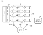
- FIG.1 is a block diagram schematically illustrating a cascaded H-bridge inverter topology according to prior art.
- the cascaded H-bridge inverter topology includes a master controller (130) and a cell controller (not shown) inside a plurality of cells (120), where control is performed by the master controller (120) and the cell controller, both of which are connected to a high speed link, whereby data is transmitted and received.
- the master controller (120) receives a motor speed and an output current of the inverter to perform the motor speed and current control, and transmits to the cell controller by synchronizing 3-phase voltage levels for each phase.
- the cell controller generates a PWM (Pulse Width Modulation) using DC link voltages of each cell (120) and voltage levels received from the master controller (120).
- the master controller (120) in the conventional cascaded H-bridge inverter detects, from a motor (200), a current of each phase for safe acceleration/deceleration of the motor (200) and a current sensor (140) is provided to this end.
- the current sensor (140) used for the motor (200) is a current-type current sensor instead of voltage-type current sensor due to the fact that a final insulation voltage is equal to a voltage of the motor (120) and a detection length of the current sensor (140) is very long. Furthermore, the current-type current sensor is robust to noise.
- detection current sensor selection of detection current sensor is restricted due to pre voltage and current conditions, and there is no way to cope with hardware loss as only one element for detecting the current of each phase is available.
- the present disclosure is to provide a multilevel inverter configured to detect a current of the multilevel inverter using a general purpose current detection element by providing a same current to serially connected cells and detecting a current from each cell. Furthermore, the present disclosure is to provide a multilevel inverter configured to be applied with a current detection element regardless of restrictive conditions relative to voltage and current conditions and noise.
- a multilevel inverter configured to output a 3-phase voltage to a motor by allowing a plurality of unit power cells forming one phase to be serially connected, the multilevel inverter comprising: a plurality of current sensors configured to detect an output current of the plurality of unit power cells.
- the multilevel inverter may further comprise a master controller configured to transmit voltage level information to the unit power cells by receiving an output current of the plurality of unit power cells.
- the unit power cell may include a rectifier configured to rectify an inputted AC voltage to a DC voltage, a DC link capacitor configured to smooth an output voltage of the rectifier, a cell controller configured to generate a PWM (Pulse Width Modulation) signal in response to the voltage level information received from the master controller, an inverter unit configured to convert a DC voltage of the DC link capacitor to an AC voltage to be outputted to a motor in response to the PWM signal of the cell controller, and the current sensor configured to detect an output current of the inverter unit.
- PWM Pulse Width Modulation
- the inverter unit may include a plurality of semiconductor devices, and the current sensor may detect a current outputted from the plurality of semiconductor devices.
- the current sensor may detect the output current of the inverter unit and may provide the output current to the master controller.
- the multi-level inverter system according to the present disclosure thus described has an advantageous effect in that system reliability can be enhanced by outputting a same set performance even if there is generated hardware defect when a system is formed, and maintenance cost of the system can be reduced due to no separate set change.
- Another advantageous effect is that a current can be detected for each set to allow detecting a current safely relative to voltage, and a more accurate value can be detected.
- FIG. 2 is a schematic block diagram illustrating a multilevel inverter according to an exemplary embodiment of the present disclosure.
- the multilevel inverter according to the present disclosure explains a cascaded H-bridge inverter, for example, the present disclosure is not limited thereto, and the present disclosure may be applied to other types of inverters.
- a multilevel inverter (10) is configured to control a motor (20) and includes a master controller (11), a plurality of unit power cells (hereinafter referred to as "cells", 12) and a phase shift transformer (13).
- the phase shift transformer (13) is configured to supply an independent electric power to each cell (12).
- the detailed explanation on configuration of the phase shift transformer will be omitted as it is not directly related to the present disclosure.
- the plurality of cells (12) includes a cell (U1, U2, 7-8Un) forming a U phase, a cell (V1, V2, 7-8Vn) forming a V phase and a cell (W1,W2, 7-8Wn) forming a W phase, where the cells are serially connected to provide each phase, and a sum of outputs of these cells may be multilevel output voltages for driving the motor (20).
- the number of cells forming a cell may be determined by the output voltages.
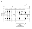
- FIG. 3 is a detailed block diagram illustrating each cell of FIG. 2 , where only one cell is described as each configuration of the plurality of cells is same.
- the unit power cell (12) according to the present disclosure includes a rectifier (31), a DC link capacitor (32), an inverter unit (33), a current sensor (34) and a cell controller (35).
- the rectifier (31) rectifies an AC voltage inputted from the phase shift transformer (13) to a DC voltage, and the DC link capacitor (32) smoothes the DC voltage inputted from the rectifier (31).
- the rectifier (31) may be formed with a plurality of diodes.
- the inverter unit (33) generates an AC voltage to be outputted to the motor (20) in response to PWM control of the cell controller (35), and outputs the AC voltage, and may be formed by a plurality of IGBTs (Insulated Gate Bipolar Transistors), for example.
- the current sensor (34) may detect a current outputted from the plurality of semiconductor devices of the inverter unit (33), and provide the current to the master controller (11).
- the master controller (11) of FIG.2 is illustrated as being formed independently from the plurality of cells (12), it is for the simplicity of drawing, and the master controller (11) and the cell controller (35) of the plurality of cells (12) may be connected via optical communication for insulation and reduction in noise.
- the master controller (11) receives an output voltage from the plurality of cells and in turn transmits voltage level information to the cells (12).
- Each cell (12) may apply an output voltage corresponding to the DC link voltage to the motor (20) which is a load, generates a PWM signal in response to the voltage level information, whereby frequency applied to the motor (20) can be varied to obtain a starting torque and control a motor speed at the same time.
- the multilevel inverter (10) is configured such that the current sensor (34) is arranged respectively on the plurality of cells (12) forming a phase voltage inputted to the motor (20) and detects an output current of the inverter unit (33) in the plurality of cells (12).
- each cell may use a voltage type current sensor because noise level is lower than that of the entire multilevel inverter (10), and therefore, a detection length is short and power supply is smooth because the current detection is performed by the cells (12). Furthermore, an over-current protection for each cell (12) is possible to thereby enable a build-up of reliable system.
- a current flowing from each phase to the cell (12) is same, and even if one cell is inoperative, a continuous current detection is enabled, and the master controller (11) can more accurately transmit control information to the cell controller (35) because the current information of cells (12) is transmitted to the master controller (11).
- a general purpose voltage type current sensor can be used in comparison to a current sensor of an inverter unit to thereby reduce costs over the conventional large capacity current sensor, and because a dielectric withstanding voltage to the current sensor is limited to the cell voltage, no additional insulation reinforcement is required.
Landscapes
- Engineering & Computer Science (AREA)
- Power Engineering (AREA)
- Physics & Mathematics (AREA)
- General Physics & Mathematics (AREA)
- Inverter Devices (AREA)
Description
- The teachings in accordance with the exemplary embodiments of this present disclosure generally relate to a multilevel inverter.
- Medium voltage high capacity multilevel inverters have emerged from development demands on medium voltage power conversion for promotion and operation of efficient and flexible power systems in electric power industries such as FACTS (Flexible AC Transmission System) devices. Recently, interests in multilevel inverters have increased as multilevel inverter topologies.
- Some of the known types of configurations for multilevel inverters are cascaded H-bridge, diode-clamped and flying capacitor multi-level inverters. The cascaded H-bridge inverter is configured by unit cells having independent DC links by serially connected low voltage H-bridge inverters, where a sum of voltages of each cell equals to a sum of inverter outputs, and the output voltages may vary according to the number of cells. However, the cascaded H-bridge inverter topology suffers from disadvantage that independent DC link power must be supplied.
-
FIG.1 is a block diagram schematically illustrating a cascaded H-bridge inverter topology according to prior art. - Referring to
FIG. 1 , the cascaded H-bridge inverter topology according to prior art includes a master controller (130) and a cell controller (not shown) inside a plurality of cells (120), where control is performed by the master controller (120) and the cell controller, both of which are connected to a high speed link, whereby data is transmitted and received. - The master controller (120) receives a motor speed and an output current of the inverter to perform the motor speed and current control, and transmits to the cell controller by synchronizing 3-phase voltage levels for each phase. The cell controller generates a PWM (Pulse Width Modulation) using DC link voltages of each cell (120) and voltage levels received from the master controller (120). The master controller (120) in the conventional cascaded H-bridge inverter detects, from a motor (200), a current of each phase for safe acceleration/deceleration of the motor (200) and a current sensor (140) is provided to this end.
- The current sensor (140) used for the motor (200) according to prior art is a current-type current sensor instead of voltage-type current sensor due to the fact that a final insulation voltage is equal to a voltage of the motor (120) and a detection length of the current sensor (140) is very long. Furthermore, the current-type current sensor is robust to noise.
- That is, selection of detection current sensor is restricted due to pre voltage and current conditions, and there is no way to cope with hardware loss as only one element for detecting the current of each phase is available.
- The present disclosure is to provide a multilevel inverter configured to detect a current of the multilevel inverter using a general purpose current detection element by providing a same current to serially connected cells and detecting a current from each cell. Furthermore, the present disclosure is to provide a multilevel inverter configured to be applied with a current detection element regardless of restrictive conditions relative to voltage and current conditions and noise.
- In one general aspect of the present disclosure, there is provided a multilevel inverter configured to output a 3-phase voltage to a motor by allowing a plurality of unit power cells forming one phase to be serially connected, the multilevel inverter comprising: a plurality of current sensors configured to detect an output current of the plurality of unit power cells.
- Preferably, but not necessarily, the multilevel inverter may further comprise a master controller configured to transmit voltage level information to the unit power cells by receiving an output current of the plurality of unit power cells.
- Preferably, but not necessarily, the unit power cell may include a rectifier configured to rectify an inputted AC voltage to a DC voltage, a DC link capacitor configured to smooth an output voltage of the rectifier, a cell controller configured to generate a PWM (Pulse Width Modulation) signal in response to the voltage level information received from the master controller, an inverter unit configured to convert a DC voltage of the DC link capacitor to an AC voltage to be outputted to a motor in response to the PWM signal of the cell controller, and the current sensor configured to detect an output current of the inverter unit.
- Preferably, but not necessarily, the inverter unit may include a plurality of semiconductor devices, and the current sensor may detect a current outputted from the plurality of semiconductor devices.
- Preferably, but not necessarily, the current sensor may detect the output current of the inverter unit and may provide the output current to the master controller.
- The multi-level inverter system according to the present disclosure thus described has an advantageous effect in that system reliability can be enhanced by outputting a same set performance even if there is generated hardware defect when a system is formed, and maintenance cost of the system can be reduced due to no separate set change.
- Another advantageous effect is that a current can be detected for each set to allow detecting a current safely relative to voltage, and a more accurate value can be detected.
-
-
FIG. 1 is a schematic block diagram illustrating a cascade H-bridge inverter according to prior art. -
FIG. 2 is a schematic block diagram illustrating a multilevel inverter according to an exemplary embodiment of the present disclosure. -
FIG. 3 is a detailed block diagram illustrating each cell ofFIG. 2 . - Various exemplary embodiments will be described more fully hereinafter with reference to the accompanying drawings, in which some exemplary embodiments are shown. The present inventive concept may, however, be embodied in many different forms and should not be construed as limited to the example embodiments set forth herein. Rather, the described aspect is intended to embrace all such alterations, modifications, and variations that fall within the scope and novel idea of the present disclosure.
-
FIG. 2 is a schematic block diagram illustrating a multilevel inverter according to an exemplary embodiment of the present disclosure. - Although the multilevel inverter according to the present disclosure explains a cascaded H-bridge inverter, for example, the present disclosure is not limited thereto, and the present disclosure may be applied to other types of inverters.
- Referring to
FIG.2 , a multilevel inverter (10) according to the present disclosure is configured to control a motor (20) and includes a master controller (11), a plurality of unit power cells (hereinafter referred to as "cells", 12) and a phase shift transformer (13). The phase shift transformer (13) is configured to supply an independent electric power to each cell (12). The detailed explanation on configuration of the phase shift transformer will be omitted as it is not directly related to the present disclosure. - The plurality of cells (12) includes a cell (U1, U2, .....Un) forming a U phase, a cell (V1, V2, .....Vn) forming a V phase and a cell (W1,W2, .....Wn) forming a W phase, where the cells are serially connected to provide each phase, and a sum of outputs of these cells may be multilevel output voltages for driving the motor (20). The number of cells forming a cell may be determined by the output voltages.
-
FIG. 3 is a detailed block diagram illustrating each cell ofFIG. 2 , where only one cell is described as each configuration of the plurality of cells is same.
Referring toFIG. 3 , the unit power cell (12) according to the present disclosure includes a rectifier (31), a DC link capacitor (32), an inverter unit (33), a current sensor (34) and a cell controller (35). - The rectifier (31) rectifies an AC voltage inputted from the phase shift transformer (13) to a DC voltage, and the DC link capacitor (32) smoothes the DC voltage inputted from the rectifier (31). The rectifier (31) may be formed with a plurality of diodes.
- The inverter unit (33) generates an AC voltage to be outputted to the motor (20) in response to PWM control of the cell controller (35), and outputs the AC voltage, and may be formed by a plurality of IGBTs (Insulated Gate Bipolar Transistors), for example. The current sensor (34) may detect a current outputted from the plurality of semiconductor devices of the inverter unit (33), and provide the current to the master controller (11). Although the master controller (11) of
FIG.2 is illustrated as being formed independently from the plurality of cells (12), it is for the simplicity of drawing, and the master controller (11) and the cell controller (35) of the plurality of cells (12) may be connected via optical communication for insulation and reduction in noise. - The master controller (11) receives an output voltage from the plurality of cells and in turn transmits voltage level information to the cells (12). Each cell (12) may apply an output voltage corresponding to the DC link voltage to the motor (20) which is a load, generates a PWM signal in response to the voltage level information, whereby frequency applied to the motor (20) can be varied to obtain a starting torque and control a motor speed at the same time.
- The multilevel inverter (10) according to the present disclosure is configured such that the current sensor (34) is arranged respectively on the plurality of cells (12) forming a phase voltage inputted to the motor (20) and detects an output current of the inverter unit (33) in the plurality of cells (12).
- By the configuration thus described, each cell may use a voltage type current sensor because noise level is lower than that of the entire multilevel inverter (10), and therefore, a detection length is short and power supply is smooth because the current detection is performed by the cells (12). Furthermore, an over-current protection for each cell (12) is possible to thereby enable a build-up of reliable system.
- In addition, a current flowing from each phase to the cell (12) is same, and even if one cell is inoperative, a continuous current detection is enabled, and the master controller (11) can more accurately transmit control information to the cell controller (35) because the current information of cells (12) is transmitted to the master controller (11).
- Still furthermore, a general purpose voltage type current sensor can be used in comparison to a current sensor of an inverter unit to thereby reduce costs over the conventional large capacity current sensor, and because a dielectric withstanding voltage to the current sensor is limited to the cell voltage, no additional insulation reinforcement is required.
- Although the present disclosure has been described in detail with reference to the foregoing embodiments and advantages, many alternatives, modifications, and variations will be apparent to those skilled in the art within the metes and bounds of the claims. Therefore, it should be understood that the above-described embodiments are not limited by any of the details of the foregoing description, unless otherwise specified, but rather should be construed broadly within the scope as defined in the appended claims
Claims (6)
- A multilevel inverter (10) configured to output a 3-phase voltage to a motor (20) by allowing a plurality of unit power cells (12) forming one phase to be serially connected, the multilevel inverter (10) characterized by:a plurality of current sensors (34) configured to detect an output current of the plurality of unit power cells.
- The multilevel inverter (10) of claim 1 further characterized by a master controller (11) configured to transmit voltage level information to the unit power cells (12) by receiving an output current of the plurality of unit power cells (12).
- The multilevel inverter (10) of claim 2, characterized in that the unit power cell (12) includes a rectifier (31) configured to rectify an inputted AC voltage to a DC voltage, a DC link capacitor (32) configured to smooth an output voltage of the rectifier, a cell controller (35) configured to generate a PWM (Pulse Width Modulation) signal in response to the voltage level information received from the master controller, an inverter unit (33) configured to convert a DC voltage of the DC link capacitor (32) to an AC voltage to be outputted to a motor in response to the PWM signal of the cell controller (35), and the current sensor (34) configured to detect an output current of the inverter unit (33).
- The multilevel inverter of claim 3, characterized in that the inverter unit (33) includes a plurality of semiconductor devices, and the current sensor (34) detects a current outputted from the plurality of semiconductor devices.
- The multilevel inverter of claim 3 or 4, characterized in that the current sensor (34) detects the output current of the inverter unit (33) and provides the output current to the master controller (11).
- The multilevel inverter of any one claim of 1 to 5, characterized in that the current sensor (34) is a voltage type current sensor.
Applications Claiming Priority (1)
| Application Number | Priority Date | Filing Date | Title |
|---|---|---|---|
| KR1020130085813A KR101583868B1 (en) | 2013-07-22 | 2013-07-22 | Multi-level inverter |
Publications (3)
| Publication Number | Publication Date |
|---|---|
| EP2830207A2 true EP2830207A2 (en) | 2015-01-28 |
| EP2830207A3 EP2830207A3 (en) | 2015-07-08 |
| EP2830207B1 EP2830207B1 (en) | 2019-11-27 |
Family
ID=51063333
Family Applications (1)
| Application Number | Title | Priority Date | Filing Date |
|---|---|---|---|
| EP14175917.5A Active EP2830207B1 (en) | 2013-07-22 | 2014-07-07 | Multilevel inverter with separately fed cell modules |
Country Status (6)
| Country | Link |
|---|---|
| US (1) | US20150022135A1 (en) |
| EP (1) | EP2830207B1 (en) |
| JP (1) | JP6027060B2 (en) |
| KR (1) | KR101583868B1 (en) |
| CN (1) | CN104333254A (en) |
| ES (1) | ES2773039T3 (en) |
Cited By (2)
| Publication number | Priority date | Publication date | Assignee | Title |
|---|---|---|---|---|
| WO2017207045A1 (en) * | 2016-06-01 | 2017-12-07 | Abb Schweiz Ag | Modular multilevel converter cell with integrated current sensor |
| EP3664273B1 (en) * | 2017-08-02 | 2024-08-21 | Meidensha Corporation | Inverter device |
Families Citing this family (6)
| Publication number | Priority date | Publication date | Assignee | Title |
|---|---|---|---|---|
| KR101491933B1 (en) * | 2013-11-19 | 2015-02-09 | 엘에스산전 주식회사 | Apparatus for controlling paralleled inverter |
| KR101950302B1 (en) * | 2014-07-23 | 2019-02-20 | 엘에스산전 주식회사 | Parallel operation control method of medium voltage inverter |
| RU2629009C2 (en) * | 2016-02-16 | 2017-08-24 | Федеральное государственное унитарное предприятие "Крыловский государственный научный центр" | Alternate current variable speed drive |
| JP6817163B2 (en) * | 2017-07-12 | 2021-01-20 | 株式会社東芝 | Power converter |
| US10116229B1 (en) | 2017-09-19 | 2018-10-30 | King Saud University | Multilevel cascade hexagonal voltage source converter with isolated DC sources |
| CN113937986B (en) * | 2021-12-16 | 2022-03-25 | 南昌工程学院 | Method, device and equipment for detecting direct-current voltage of cascaded H-bridge power module |
Family Cites Families (15)
| Publication number | Priority date | Publication date | Assignee | Title |
|---|---|---|---|---|
| US4875000A (en) * | 1986-11-26 | 1989-10-17 | The Babcock & Wilcox Company | Current fault detection system and method for AC controller |
| US5638263A (en) * | 1994-03-01 | 1997-06-10 | Halmar Robicon Group | Low and medium voltage PWM AC/DC power conversion method and apparatus |
| KR100786696B1 (en) * | 2002-10-21 | 2007-12-21 | 현대중공업 주식회사 | H-bridge inverter system using serial communication |
| JP2005160136A (en) * | 2003-11-20 | 2005-06-16 | Toyota Motor Corp | Inverter device and automobile having the same |
| US7825540B2 (en) * | 2006-03-27 | 2010-11-02 | Mitsubishi Electric Corporation | Power conversion device |
| KR20090100655A (en) * | 2008-03-20 | 2009-09-24 | 엘에스산전 주식회사 | Multi-level inverter |
| US7940537B2 (en) * | 2008-12-31 | 2011-05-10 | Teco-Westinghouse Motor Company | Partial regeneration in a multi-level power inverter |
| JP5224128B2 (en) * | 2009-01-14 | 2013-07-03 | ダイキン工業株式会社 | Current detection circuit |
| KR101025647B1 (en) * | 2009-08-28 | 2011-03-30 | 엘에스산전 주식회사 | Control device and method of high voltage inverter |
| JP5592236B2 (en) * | 2010-11-01 | 2014-09-17 | 株式会社日立製作所 | Power converter |
| JP2012156199A (en) * | 2011-01-24 | 2012-08-16 | Yaskawa Electric Corp | Electric power conversion apparatus and electric apparatus |
| CN102135013B (en) * | 2011-02-14 | 2013-02-27 | 上海理工大学 | An automatic control system and automatic control method for coal flow reloading in a two-stage coal bunker in a mine |
| CN102111080B (en) * | 2011-02-24 | 2013-09-18 | 广州智光电气股份有限公司 | Photovoltaic grid-connected inverter and control method |
| JP5360125B2 (en) * | 2011-04-26 | 2013-12-04 | 株式会社安川電機 | Series multiple power converter |
| US9153374B2 (en) * | 2013-06-28 | 2015-10-06 | Teco-Westinghouse Motor Company | Cooling arrangements for drive systems |
-
2013
- 2013-07-22 KR KR1020130085813A patent/KR101583868B1/en active Active
-
2014
- 2014-06-20 US US14/311,066 patent/US20150022135A1/en not_active Abandoned
- 2014-07-07 EP EP14175917.5A patent/EP2830207B1/en active Active
- 2014-07-07 ES ES14175917T patent/ES2773039T3/en active Active
- 2014-07-22 JP JP2014149033A patent/JP6027060B2/en active Active
- 2014-07-22 CN CN201410350189.7A patent/CN104333254A/en active Pending
Non-Patent Citations (1)
| Title |
|---|
| None |
Cited By (3)
| Publication number | Priority date | Publication date | Assignee | Title |
|---|---|---|---|---|
| WO2017207045A1 (en) * | 2016-06-01 | 2017-12-07 | Abb Schweiz Ag | Modular multilevel converter cell with integrated current sensor |
| US10622913B2 (en) | 2016-06-01 | 2020-04-14 | Abb Schweiz Ag | Modular multilevel converter cell with integrated current sensor |
| EP3664273B1 (en) * | 2017-08-02 | 2024-08-21 | Meidensha Corporation | Inverter device |
Also Published As
| Publication number | Publication date |
|---|---|
| JP2015023799A (en) | 2015-02-02 |
| EP2830207B1 (en) | 2019-11-27 |
| ES2773039T3 (en) | 2020-07-09 |
| US20150022135A1 (en) | 2015-01-22 |
| JP6027060B2 (en) | 2016-11-16 |
| KR101583868B1 (en) | 2016-01-08 |
| CN104333254A (en) | 2015-02-04 |
| EP2830207A3 (en) | 2015-07-08 |
| KR20150011064A (en) | 2015-01-30 |
Similar Documents
| Publication | Publication Date | Title |
|---|---|---|
| EP2830207B1 (en) | Multilevel inverter with separately fed cell modules | |
| CN105141193B (en) | Control device of electric motor with least two conductive discharge units | |
| EP2975754B1 (en) | Energy conversion system and method | |
| JP6809769B2 (en) | Power converter control system and method | |
| KR101491933B1 (en) | Apparatus for controlling paralleled inverter | |
| US11196355B2 (en) | Power conversion apparatus having autonomous generation of identification information by each sub-module | |
| EP3309949B1 (en) | Power conversion device | |
| US20110188271A1 (en) | Switching regulator device | |
| US20120275202A1 (en) | Series multiplex power conversion apparatus | |
| US20190243715A1 (en) | Drive apparatus for switch | |
| US9837950B2 (en) | Vehicle control device and railroad vehicle | |
| US10027265B2 (en) | Inverter control device and inverter control method | |
| JP5111208B2 (en) | Power converter | |
| JP2012034528A (en) | Power conversion device | |
| JP2008187874A (en) | Phase interruption detector of three-phase ac power supply | |
| JP6156784B1 (en) | INVERTER DEVICE AND INVERTER DEVICE CONTROL METHOD | |
| KR101414887B1 (en) | Multi-level inverter and method for operating the same | |
| CN110710091A (en) | Control device for DC/DC converter | |
| JP7601605B2 (en) | POWER CONVERSION DEVICE, POWER CONVERSION CONTROL METHOD, AND POWER CONVERSION CONTROL PROGRAM | |
| JP2016093074A (en) | Inverter system | |
| WO2021049230A1 (en) | Power conversion device and method for controlling power conversion device | |
| WO2017046965A1 (en) | Inverter device, and method for manufacturing inverter device | |
| JP5050900B2 (en) | Driving device for power conversion circuit and power conversion device | |
| JP2012065380A (en) | Motor control apparatus | |
| JP2009177883A (en) | Power converter signal transmission device |
Legal Events
| Date | Code | Title | Description |
|---|---|---|---|
| 17P | Request for examination filed |
Effective date: 20140707 |
|
| AK | Designated contracting states |
Kind code of ref document: A2 Designated state(s): AL AT BE BG CH CY CZ DE DK EE ES FI FR GB GR HR HU IE IS IT LI LT LU LV MC MK MT NL NO PL PT RO RS SE SI SK SM TR |
|
| AX | Request for extension of the european patent |
Extension state: BA ME |
|
| PUAI | Public reference made under article 153(3) epc to a published international application that has entered the european phase |
Free format text: ORIGINAL CODE: 0009012 |
|
| PUAL | Search report despatched |
Free format text: ORIGINAL CODE: 0009013 |
|
| AK | Designated contracting states |
Kind code of ref document: A3 Designated state(s): AL AT BE BG CH CY CZ DE DK EE ES FI FR GB GR HR HU IE IS IT LI LT LU LV MC MK MT NL NO PL PT RO RS SE SI SK SM TR |
|
| AX | Request for extension of the european patent |
Extension state: BA ME |
|
| RIC1 | Information provided on ipc code assigned before grant |
Ipc: H02P 27/06 20060101ALN20150601BHEP Ipc: H02M 1/00 20070101ALI20150601BHEP Ipc: H02M 7/49 20070101AFI20150601BHEP |
|
| R17P | Request for examination filed (corrected) |
Effective date: 20160107 |
|
| RBV | Designated contracting states (corrected) |
Designated state(s): AL AT BE BG CH CY CZ DE DK EE ES FI FR GB GR HR HU IE IS IT LI LT LU LV MC MK MT NL NO PL PT RO RS SE SI SK SM TR |
|
| STAA | Information on the status of an ep patent application or granted ep patent |
Free format text: STATUS: EXAMINATION IS IN PROGRESS |
|
| 17Q | First examination report despatched |
Effective date: 20170418 |
|
| GRAP | Despatch of communication of intention to grant a patent |
Free format text: ORIGINAL CODE: EPIDOSNIGR1 |
|
| STAA | Information on the status of an ep patent application or granted ep patent |
Free format text: STATUS: GRANT OF PATENT IS INTENDED |
|
| INTG | Intention to grant announced |
Effective date: 20190814 |
|
| GRAS | Grant fee paid |
Free format text: ORIGINAL CODE: EPIDOSNIGR3 |
|
| GRAA | (expected) grant |
Free format text: ORIGINAL CODE: 0009210 |
|
| STAA | Information on the status of an ep patent application or granted ep patent |
Free format text: STATUS: THE PATENT HAS BEEN GRANTED |
|
| AK | Designated contracting states |
Kind code of ref document: B1 Designated state(s): AL AT BE BG CH CY CZ DE DK EE ES FI FR GB GR HR HU IE IS IT LI LT LU LV MC MK MT NL NO PL PT RO RS SE SI SK SM TR |
|
| REG | Reference to a national code |
Ref country code: GB Ref legal event code: FG4D |
|
| REG | Reference to a national code |
Ref country code: CH Ref legal event code: EP |
|
| REG | Reference to a national code |
Ref country code: AT Ref legal event code: REF Ref document number: 1207865 Country of ref document: AT Kind code of ref document: T Effective date: 20191215 |
|
| REG | Reference to a national code |
Ref country code: DE Ref legal event code: R096 Ref document number: 602014057393 Country of ref document: DE |
|
| REG | Reference to a national code |
Ref country code: IE Ref legal event code: FG4D |
|
| REG | Reference to a national code |
Ref country code: NL Ref legal event code: MP Effective date: 20191127 |
|
| REG | Reference to a national code |
Ref country code: LT Ref legal event code: MG4D |
|
| PG25 | Lapsed in a contracting state [announced via postgrant information from national office to epo] |
Ref country code: NO Free format text: LAPSE BECAUSE OF FAILURE TO SUBMIT A TRANSLATION OF THE DESCRIPTION OR TO PAY THE FEE WITHIN THE PRESCRIBED TIME-LIMIT Effective date: 20200227 Ref country code: BG Free format text: LAPSE BECAUSE OF FAILURE TO SUBMIT A TRANSLATION OF THE DESCRIPTION OR TO PAY THE FEE WITHIN THE PRESCRIBED TIME-LIMIT Effective date: 20200227 Ref country code: GR Free format text: LAPSE BECAUSE OF FAILURE TO SUBMIT A TRANSLATION OF THE DESCRIPTION OR TO PAY THE FEE WITHIN THE PRESCRIBED TIME-LIMIT Effective date: 20200228 Ref country code: LT Free format text: LAPSE BECAUSE OF FAILURE TO SUBMIT A TRANSLATION OF THE DESCRIPTION OR TO PAY THE FEE WITHIN THE PRESCRIBED TIME-LIMIT Effective date: 20191127 Ref country code: FI Free format text: LAPSE BECAUSE OF FAILURE TO SUBMIT A TRANSLATION OF THE DESCRIPTION OR TO PAY THE FEE WITHIN THE PRESCRIBED TIME-LIMIT Effective date: 20191127 Ref country code: SE Free format text: LAPSE BECAUSE OF FAILURE TO SUBMIT A TRANSLATION OF THE DESCRIPTION OR TO PAY THE FEE WITHIN THE PRESCRIBED TIME-LIMIT Effective date: 20191127 Ref country code: LV Free format text: LAPSE BECAUSE OF FAILURE TO SUBMIT A TRANSLATION OF THE DESCRIPTION OR TO PAY THE FEE WITHIN THE PRESCRIBED TIME-LIMIT Effective date: 20191127 Ref country code: NL Free format text: LAPSE BECAUSE OF FAILURE TO SUBMIT A TRANSLATION OF THE DESCRIPTION OR TO PAY THE FEE WITHIN THE PRESCRIBED TIME-LIMIT Effective date: 20191127 |
|
| PG25 | Lapsed in a contracting state [announced via postgrant information from national office to epo] |
Ref country code: IS Free format text: LAPSE BECAUSE OF FAILURE TO SUBMIT A TRANSLATION OF THE DESCRIPTION OR TO PAY THE FEE WITHIN THE PRESCRIBED TIME-LIMIT Effective date: 20200327 Ref country code: HR Free format text: LAPSE BECAUSE OF FAILURE TO SUBMIT A TRANSLATION OF THE DESCRIPTION OR TO PAY THE FEE WITHIN THE PRESCRIBED TIME-LIMIT Effective date: 20191127 Ref country code: RS Free format text: LAPSE BECAUSE OF FAILURE TO SUBMIT A TRANSLATION OF THE DESCRIPTION OR TO PAY THE FEE WITHIN THE PRESCRIBED TIME-LIMIT Effective date: 20191127 |
|
| PG25 | Lapsed in a contracting state [announced via postgrant information from national office to epo] |
Ref country code: AL Free format text: LAPSE BECAUSE OF FAILURE TO SUBMIT A TRANSLATION OF THE DESCRIPTION OR TO PAY THE FEE WITHIN THE PRESCRIBED TIME-LIMIT Effective date: 20191127 |
|
| REG | Reference to a national code |
Ref country code: ES Ref legal event code: FG2A Ref document number: 2773039 Country of ref document: ES Kind code of ref document: T3 Effective date: 20200709 |
|
| PG25 | Lapsed in a contracting state [announced via postgrant information from national office to epo] |
Ref country code: DK Free format text: LAPSE BECAUSE OF FAILURE TO SUBMIT A TRANSLATION OF THE DESCRIPTION OR TO PAY THE FEE WITHIN THE PRESCRIBED TIME-LIMIT Effective date: 20191127 Ref country code: PT Free format text: LAPSE BECAUSE OF FAILURE TO SUBMIT A TRANSLATION OF THE DESCRIPTION OR TO PAY THE FEE WITHIN THE PRESCRIBED TIME-LIMIT Effective date: 20200419 Ref country code: EE Free format text: LAPSE BECAUSE OF FAILURE TO SUBMIT A TRANSLATION OF THE DESCRIPTION OR TO PAY THE FEE WITHIN THE PRESCRIBED TIME-LIMIT Effective date: 20191127 Ref country code: RO Free format text: LAPSE BECAUSE OF FAILURE TO SUBMIT A TRANSLATION OF THE DESCRIPTION OR TO PAY THE FEE WITHIN THE PRESCRIBED TIME-LIMIT Effective date: 20191127 Ref country code: CZ Free format text: LAPSE BECAUSE OF FAILURE TO SUBMIT A TRANSLATION OF THE DESCRIPTION OR TO PAY THE FEE WITHIN THE PRESCRIBED TIME-LIMIT Effective date: 20191127 |
|
| REG | Reference to a national code |
Ref country code: DE Ref legal event code: R097 Ref document number: 602014057393 Country of ref document: DE |
|
| PG25 | Lapsed in a contracting state [announced via postgrant information from national office to epo] |
Ref country code: SM Free format text: LAPSE BECAUSE OF FAILURE TO SUBMIT A TRANSLATION OF THE DESCRIPTION OR TO PAY THE FEE WITHIN THE PRESCRIBED TIME-LIMIT Effective date: 20191127 Ref country code: SK Free format text: LAPSE BECAUSE OF FAILURE TO SUBMIT A TRANSLATION OF THE DESCRIPTION OR TO PAY THE FEE WITHIN THE PRESCRIBED TIME-LIMIT Effective date: 20191127 |
|
| REG | Reference to a national code |
Ref country code: AT Ref legal event code: MK05 Ref document number: 1207865 Country of ref document: AT Kind code of ref document: T Effective date: 20191127 |
|
| PLBE | No opposition filed within time limit |
Free format text: ORIGINAL CODE: 0009261 |
|
| STAA | Information on the status of an ep patent application or granted ep patent |
Free format text: STATUS: NO OPPOSITION FILED WITHIN TIME LIMIT |
|
| 26N | No opposition filed |
Effective date: 20200828 |
|
| PG25 | Lapsed in a contracting state [announced via postgrant information from national office to epo] |
Ref country code: PL Free format text: LAPSE BECAUSE OF FAILURE TO SUBMIT A TRANSLATION OF THE DESCRIPTION OR TO PAY THE FEE WITHIN THE PRESCRIBED TIME-LIMIT Effective date: 20191127 Ref country code: AT Free format text: LAPSE BECAUSE OF FAILURE TO SUBMIT A TRANSLATION OF THE DESCRIPTION OR TO PAY THE FEE WITHIN THE PRESCRIBED TIME-LIMIT Effective date: 20191127 Ref country code: SI Free format text: LAPSE BECAUSE OF FAILURE TO SUBMIT A TRANSLATION OF THE DESCRIPTION OR TO PAY THE FEE WITHIN THE PRESCRIBED TIME-LIMIT Effective date: 20191127 |
|
| PG25 | Lapsed in a contracting state [announced via postgrant information from national office to epo] |
Ref country code: MC Free format text: LAPSE BECAUSE OF FAILURE TO SUBMIT A TRANSLATION OF THE DESCRIPTION OR TO PAY THE FEE WITHIN THE PRESCRIBED TIME-LIMIT Effective date: 20191127 |
|
| REG | Reference to a national code |
Ref country code: CH Ref legal event code: PL |
|
| REG | Reference to a national code |
Ref country code: BE Ref legal event code: MM Effective date: 20200731 |
|
| PG25 | Lapsed in a contracting state [announced via postgrant information from national office to epo] |
Ref country code: LU Free format text: LAPSE BECAUSE OF NON-PAYMENT OF DUE FEES Effective date: 20200707 Ref country code: IE Free format text: LAPSE BECAUSE OF NON-PAYMENT OF DUE FEES Effective date: 20200707 Ref country code: LI Free format text: LAPSE BECAUSE OF NON-PAYMENT OF DUE FEES Effective date: 20200731 Ref country code: CH Free format text: LAPSE BECAUSE OF NON-PAYMENT OF DUE FEES Effective date: 20200731 |
|
| PG25 | Lapsed in a contracting state [announced via postgrant information from national office to epo] |
Ref country code: BE Free format text: LAPSE BECAUSE OF NON-PAYMENT OF DUE FEES Effective date: 20200731 |
|
| PG25 | Lapsed in a contracting state [announced via postgrant information from national office to epo] |
Ref country code: TR Free format text: LAPSE BECAUSE OF FAILURE TO SUBMIT A TRANSLATION OF THE DESCRIPTION OR TO PAY THE FEE WITHIN THE PRESCRIBED TIME-LIMIT Effective date: 20191127 Ref country code: MT Free format text: LAPSE BECAUSE OF FAILURE TO SUBMIT A TRANSLATION OF THE DESCRIPTION OR TO PAY THE FEE WITHIN THE PRESCRIBED TIME-LIMIT Effective date: 20191127 Ref country code: CY Free format text: LAPSE BECAUSE OF FAILURE TO SUBMIT A TRANSLATION OF THE DESCRIPTION OR TO PAY THE FEE WITHIN THE PRESCRIBED TIME-LIMIT Effective date: 20191127 |
|
| PG25 | Lapsed in a contracting state [announced via postgrant information from national office to epo] |
Ref country code: MK Free format text: LAPSE BECAUSE OF FAILURE TO SUBMIT A TRANSLATION OF THE DESCRIPTION OR TO PAY THE FEE WITHIN THE PRESCRIBED TIME-LIMIT Effective date: 20191127 |
|
| P01 | Opt-out of the competence of the unified patent court (upc) registered |
Effective date: 20230625 |
|
| PGFP | Annual fee paid to national office [announced via postgrant information from national office to epo] |
Ref country code: GB Payment date: 20250610 Year of fee payment: 12 |
|
| PGFP | Annual fee paid to national office [announced via postgrant information from national office to epo] |
Ref country code: FR Payment date: 20250611 Year of fee payment: 12 |
|
| PGFP | Annual fee paid to national office [announced via postgrant information from national office to epo] |
Ref country code: ES Payment date: 20250822 Year of fee payment: 12 |
|
| PGFP | Annual fee paid to national office [announced via postgrant information from national office to epo] |
Ref country code: DE Payment date: 20250609 Year of fee payment: 12 |
|
| PGFP | Annual fee paid to national office [announced via postgrant information from national office to epo] |
Ref country code: IT Payment date: 20250610 Year of fee payment: 12 |