EP2830096A1 - III-V semiconductor device with interfacial layer - Google Patents
III-V semiconductor device with interfacial layer Download PDFInfo
- Publication number
- EP2830096A1 EP2830096A1 EP13177959.7A EP13177959A EP2830096A1 EP 2830096 A1 EP2830096 A1 EP 2830096A1 EP 13177959 A EP13177959 A EP 13177959A EP 2830096 A1 EP2830096 A1 EP 2830096A1
- Authority
- EP
- European Patent Office
- Prior art keywords
- substrate
- interfacial layer
- semiconductor structure
- iii
- layer
- Prior art date
- Legal status (The legal status is an assumption and is not a legal conclusion. Google has not performed a legal analysis and makes no representation as to the accuracy of the status listed.)
- Granted
Links
Images



Classifications
-
- H—ELECTRICITY
- H10—SEMICONDUCTOR DEVICES; ELECTRIC SOLID-STATE DEVICES NOT OTHERWISE PROVIDED FOR
- H10D—INORGANIC ELECTRIC SEMICONDUCTOR DEVICES
- H10D64/00—Electrodes of devices having potential barriers
- H10D64/60—Electrodes characterised by their materials
- H10D64/66—Electrodes having a conductor capacitively coupled to a semiconductor by an insulator, e.g. MIS electrodes
- H10D64/68—Electrodes having a conductor capacitively coupled to a semiconductor by an insulator, e.g. MIS electrodes characterised by the insulator, e.g. by the gate insulator
- H10D64/681—Electrodes having a conductor capacitively coupled to a semiconductor by an insulator, e.g. MIS electrodes characterised by the insulator, e.g. by the gate insulator having a compositional variation, e.g. multilayered
- H10D64/685—Electrodes having a conductor capacitively coupled to a semiconductor by an insulator, e.g. MIS electrodes characterised by the insulator, e.g. by the gate insulator having a compositional variation, e.g. multilayered being perpendicular to the channel plane
-
- H—ELECTRICITY
- H10—SEMICONDUCTOR DEVICES; ELECTRIC SOLID-STATE DEVICES NOT OTHERWISE PROVIDED FOR
- H10D—INORGANIC ELECTRIC SEMICONDUCTOR DEVICES
- H10D30/00—Field-effect transistors [FET]
- H10D30/60—Insulated-gate field-effect transistors [IGFET]
- H10D30/67—Thin-film transistors [TFT]
- H10D30/6758—Thin-film transistors [TFT] characterised by the insulating substrates
-
- H—ELECTRICITY
- H10—SEMICONDUCTOR DEVICES; ELECTRIC SOLID-STATE DEVICES NOT OTHERWISE PROVIDED FOR
- H10D—INORGANIC ELECTRIC SEMICONDUCTOR DEVICES
- H10D30/00—Field-effect transistors [FET]
- H10D30/60—Insulated-gate field-effect transistors [IGFET]
- H10D30/67—Thin-film transistors [TFT]
- H10D30/674—Thin-film transistors [TFT] characterised by the active materials
- H10D30/6755—Oxide semiconductors, e.g. zinc oxide, copper aluminium oxide or cadmium stannate
-
- H—ELECTRICITY
- H10—SEMICONDUCTOR DEVICES; ELECTRIC SOLID-STATE DEVICES NOT OTHERWISE PROVIDED FOR
- H10D—INORGANIC ELECTRIC SEMICONDUCTOR DEVICES
- H10D62/00—Semiconductor bodies, or regions thereof, of devices having potential barriers
- H10D62/80—Semiconductor bodies, or regions thereof, of devices having potential barriers characterised by the materials
- H10D62/85—Semiconductor bodies, or regions thereof, of devices having potential barriers characterised by the materials being Group III-V materials, e.g. GaAs
- H10D62/8503—Nitride Group III-V materials, e.g. AlN or GaN
-
- H—ELECTRICITY
- H10—SEMICONDUCTOR DEVICES; ELECTRIC SOLID-STATE DEVICES NOT OTHERWISE PROVIDED FOR
- H10D—INORGANIC ELECTRIC SEMICONDUCTOR DEVICES
- H10D64/00—Electrodes of devices having potential barriers
- H10D64/01—Manufacture or treatment
- H10D64/013—Manufacture or treatment of electrodes having a conductor capacitively coupled to a semiconductor by an insulator
- H10D64/01358—Manufacture or treatment of electrodes having a conductor capacitively coupled to a semiconductor by an insulator the insulator being formed after the semiconductor body, the semiconductor being a Group III-V material
-
- H—ELECTRICITY
- H10—SEMICONDUCTOR DEVICES; ELECTRIC SOLID-STATE DEVICES NOT OTHERWISE PROVIDED FOR
- H10D—INORGANIC ELECTRIC SEMICONDUCTOR DEVICES
- H10D64/00—Electrodes of devices having potential barriers
- H10D64/60—Electrodes characterised by their materials
- H10D64/66—Electrodes having a conductor capacitively coupled to a semiconductor by an insulator, e.g. MIS electrodes
- H10D64/68—Electrodes having a conductor capacitively coupled to a semiconductor by an insulator, e.g. MIS electrodes characterised by the insulator, e.g. by the gate insulator
- H10D64/691—Electrodes having a conductor capacitively coupled to a semiconductor by an insulator, e.g. MIS electrodes characterised by the insulator, e.g. by the gate insulator comprising metallic compounds, e.g. metal oxides or metal silicates
-
- H—ELECTRICITY
- H10—SEMICONDUCTOR DEVICES; ELECTRIC SOLID-STATE DEVICES NOT OTHERWISE PROVIDED FOR
- H10P—GENERIC PROCESSES OR APPARATUS FOR THE MANUFACTURE OR TREATMENT OF DEVICES COVERED BY CLASS H10
- H10P14/00—Formation of materials, e.g. in the shape of layers or pillars
- H10P14/60—Formation of materials, e.g. in the shape of layers or pillars of insulating materials
- H10P14/69—Inorganic materials
- H10P14/692—Inorganic materials composed of oxides, glassy oxides or oxide-based glasses
- H10P14/6938—Inorganic materials composed of oxides, glassy oxides or oxide-based glasses the material containing at least one metal element, e.g. metal oxides, metal oxynitrides or metal oxycarbides
- H10P14/6939—Inorganic materials composed of oxides, glassy oxides or oxide-based glasses the material containing at least one metal element, e.g. metal oxides, metal oxynitrides or metal oxycarbides characterised by the metal
- H10P14/69396—Inorganic materials composed of oxides, glassy oxides or oxide-based glasses the material containing at least one metal element, e.g. metal oxides, metal oxynitrides or metal oxycarbides characterised by the metal the material containing at least one rare earth metal element, e.g. oxides of lanthanides, scandium or yttrium
-
- H—ELECTRICITY
- H10—SEMICONDUCTOR DEVICES; ELECTRIC SOLID-STATE DEVICES NOT OTHERWISE PROVIDED FOR
- H10D—INORGANIC ELECTRIC SEMICONDUCTOR DEVICES
- H10D62/00—Semiconductor bodies, or regions thereof, of devices having potential barriers
- H10D62/80—Semiconductor bodies, or regions thereof, of devices having potential barriers characterised by the materials
- H10D62/85—Semiconductor bodies, or regions thereof, of devices having potential barriers characterised by the materials being Group III-V materials, e.g. GaAs
-
- H—ELECTRICITY
- H10—SEMICONDUCTOR DEVICES; ELECTRIC SOLID-STATE DEVICES NOT OTHERWISE PROVIDED FOR
- H10P—GENERIC PROCESSES OR APPARATUS FOR THE MANUFACTURE OR TREATMENT OF DEVICES COVERED BY CLASS H10
- H10P14/00—Formation of materials, e.g. in the shape of layers or pillars
- H10P14/60—Formation of materials, e.g. in the shape of layers or pillars of insulating materials
- H10P14/69—Inorganic materials
- H10P14/692—Inorganic materials composed of oxides, glassy oxides or oxide-based glasses
- H10P14/6938—Inorganic materials composed of oxides, glassy oxides or oxide-based glasses the material containing at least one metal element, e.g. metal oxides, metal oxynitrides or metal oxycarbides
-
- H—ELECTRICITY
- H10—SEMICONDUCTOR DEVICES; ELECTRIC SOLID-STATE DEVICES NOT OTHERWISE PROVIDED FOR
- H10P—GENERIC PROCESSES OR APPARATUS FOR THE MANUFACTURE OR TREATMENT OF DEVICES COVERED BY CLASS H10
- H10P14/00—Formation of materials, e.g. in the shape of layers or pillars
- H10P14/60—Formation of materials, e.g. in the shape of layers or pillars of insulating materials
- H10P14/69—Inorganic materials
- H10P14/692—Inorganic materials composed of oxides, glassy oxides or oxide-based glasses
- H10P14/6938—Inorganic materials composed of oxides, glassy oxides or oxide-based glasses the material containing at least one metal element, e.g. metal oxides, metal oxynitrides or metal oxycarbides
- H10P14/6939—Inorganic materials composed of oxides, glassy oxides or oxide-based glasses the material containing at least one metal element, e.g. metal oxides, metal oxynitrides or metal oxycarbides characterised by the metal
- H10P14/69391—Inorganic materials composed of oxides, glassy oxides or oxide-based glasses the material containing at least one metal element, e.g. metal oxides, metal oxynitrides or metal oxycarbides characterised by the metal the material containing aluminium, e.g. Al2O3
Definitions
- the present invention relates to the field of semiconductor structures for use in III-V MOS devices, and more specifically to gate stacks for n-FETs.
- high-k dielectrics have been used.
- high-k dielectrics have a small bandgap, which can also contribute to high tunnelling leakage current.
- the decrease in equivalent oxide thickness should not be accompanied by a decrease in charge mobility in the III-V substrate. Indeed, this mobility is particularly important in Field Effect Transistors.
- US 2006/0054937 proposes to tackle these issues by inserting between the substrate and the primary dielectric layer an oxide layer including a group III element from the substrate, and by further inserting between said oxide layer and the primary dielectric layer an interfacial dielectric layer.
- the interfacial dielectric layer includes HfO 2 , ZrO 2 , a zirconium silicate alloy, and/or a hafnium silicate alloy.
- III-V semiconductor structure For the fabrication of a semi-conductor device comprising a III-V substrate and a high-k dielectric, it would be advantageous to achieve the manufacture of a III-V semiconductor structure enabling:
- a semiconductor structure comprises a substrate comprising a III-V material, and an interfacial layer overlaying said substrate.
- This structure is well suited for further comprising a high-k dielectric layer overlaying said interfacial layer.
- the present invention relates to a semiconductor structure comprising:
- Embodiments of the semiconductor structures of the present invention may present on or more, or even all of the following advantages:
- the substrate comprising a III-V material may have a top surface comprising said III-V material. In this way, the high-k interfacial layer overlaying said substrate will be in physical contact with said III-V material.
- the substrate comprising a III-V material may be made up entirely from a III-V material.
- III-V material relates to a material comprising or made of a chemical compound with at least one group III (IUPAC group 13) element and at least one group V (IUPAC group 15) element. This includes binary compounds but also higher order compounds such as ternary compounds. It also includes mixture of such compounds.
- III-V materials e.g. GaN
- III-N materials are less preferred.
- a reason for this is their relatively large bandgaps (>3 eV) making them less suitable for the fabrication of FETs.
- said III-V material may be selected from InP, In z Ga 1-z As and Al z Ga 1-z As wherein z is from 0 to 1. These III-V materials typically show a good charge mobility.
- z may preferably be from 0.1 to 1. This is advantageous because it improves charge mobility.
- z may more preferably be from 0.3 to 1. This is advantageous because larger z values lower the conduction band minimum energy level for the III-V material, thereby increasing the conduction band offset between the III-V material and the high-k dielectric layer if present. This in turn reduces the occurrence of leakage current.
- said high-k interfacial layer may be in direct contact with said III-V material.
- said high-k interfacial layer comprising a rare earth aluminate may be made up entirely of a rare earth aluminate.
- the term “high-k” relates to a relative permittivity of 4 or more unless otherwise specified.
- Rare earth elements are the following elements: Sc, Y, La, Ce, Pr, Nd, Pm, Sm, Eu, Gd, Tb, Dy, Ho, Er, Tm, Yb, and Lu.
- the semi-conductor structure comprising only the substrate and the interfacial layer is typically an intermediate structure particularly well suited for being overlaid by a high-k dielectric layer.
- the semiconductor structure may further comprise a high-k dielectric layer overlying said interfacial layer.
- This structure is a core structure of several device types and in particular of Field Effect Transistors, wherein a portion of the substrate will serve as a channel and wherein the high-k dielectric layer will serve as a gate dielectric on which a gate electrode can be deposited.
- the chemical nature of the overlaying high-k dielectric layer is different from the chemical nature of the interfacial layer. This is however not obligatory and in some embodiment, the chemical nature of the interfacial layer and the chemical nature of the high-k dielectric layer may be the same. In some embodiments, an interfacial layer having a relatively large thickness of from 1 to 4 nm could fulfil both functions and serve as both an interfacial layer and a high-k dielectric layer.
- the overlaying high-k dielectric layer does not comprise a rare earth aluminate. This is advantageous because rare earth aluminates may have a lower k-value than other high-k dielectric materials (such as HfO 2 ).
- the high-k dielectric layer may have a higher k value than the interfacial layer.
- Rare earth aluminates in general and the three above compounds in particular are advantageous because they permit to decrease the interface defect density between the III-V substrate and the dielectric.
- Sc x Al y O 3 is advantageous because it has a low hygroscopy. This permits the use of water in the process for depositing a subsequent high-k dielectric layer. Since such deposition is preferably performed via Atomic Layer Deposition (ALD), the use of H 2 O as the oxidant has the advantage of avoiding reoxidation of the rare earth aluminate during the subsequent high-k dielectric layer deposition.
- x may be from 0.4 to 1.0. This is sometimes advantageous because values above 1.0 typically gives worse insulating properties and lower band-gap than x values at 1.0 or below. However, x values higher than 1.0 typically give a better interface than x values at or below 1.0.
- a range of x values from 1.0 to 1.6 may therefore be advantageous for use in high performance devices which can accommodate higher current leakage or for very small equivalent oxide thickness where the charge mobility is more crucial than the amount of leakage.
- Higher x values increase the k value of the oxides, hence achieving smaller equivalent oxide thickness.
- An example of a high performance device is an InGaAs channel MOSFET with high Indium content (e.g. 70%). Higher Indium content gives rise to higher drive current and transconductance while the device can tolerate higher gate leakage.
- x may be from 1.0 to 1.6 while the III-V material is In z Ga 1-z As wherein z is from 0.6 to 0.9.
- the equivalent oxide thickness (EOT) of the stack of the high-k interfacial layer and the high-k dielectric layer may be below 1 nm.
- the high-k interfacial layer may comprise Gd x Al y O 3 , Sc x Al y O 3 or La x Al y O 3 wherein x is at least 1.0.
- x is at least 1.0.
- lower x values deteriorate the insulating properties and permits higher current leakages, which is not desired.
- lower x values generally improve the quality of the interface by reducing the defect density. This in turn improves the charge mobility. Therefore, in some embodiments, it is advantageous to have a x value of from 0.4 to 1.0. Below 0.4, the insulating properties are only good enough for few applications.
- the high-k interfacial layer may comprise Gd x Al y O 3 wherein x is at least 1.0. This is advantageous because in the case of Gd x Al y O 3 , the increase in interface quality becomes low or even marginal below 1.0.
- the high-k interfacial layer may comprise Sc x Al y O 3 wherein x is at most 1.0. This is advantageous because, contrarily to Gd x Al y O 3 , the increase in interface quality below 1.0 remains significant for Sc x Al y O 3 . Furthermore, the insulating properties suffer less than in the case of Gd x Al y O 3 .
- the high-k dielectric layer may for instance be selected from HfO 2 , TiO 2 and ZnO 2 . They are advantageous due to their very high k values. Although AlO 2 could be used as the high-k dielectric layer, it is less preferred in view of its lower k value.
- an interface between the substrate and the high-k interfacial layer may have an interface defect density lower than 10 13 , preferably lower than 7*10 12 , yet more preferably lower than 5*10 12 , still more preferably lower than 3*10 12 , yet still more preferably lower than 2*10 12 and most preferably lower than 1.3*10 12 defects/cm 2 when measured in the middle of the bandgap of the III-V material.
- an interface between the substrate and the high-k interfacial layer may for instance have an interface defect density of from 5*10 11 to 1*10 13 defects/cm 2 , preferably from 8*10 11 to 7*10 12 defects/cm 2 when measured in the middle of the bandgap of the III-V material.
- an interface between the substrate and the high-k interfacial layer may have an interface defect density lower than 5*10 12 , preferably lower than 3*10 12 , yet more preferably lower than 1*10 12 , still more preferably lower than 0.9*10 12 , yet still more preferably lower than 0.6*10 12 and most preferably lower than 0.3*10 12 defects/cm 2 when measured at at least one energy level within the bandgap of the III-V material.
- the defect density will typically be lowest at the energy level of the conduction band edge of the III-V material but, due to current instrumental limitations and/or to the low thickness of the Re x Al y O 3 ( ⁇ 5 nm), an accurate Dit value cannot always be determined accurately at the conduction band edge.
- an interface between the substrate and the high-k interfacial layer may have an interface defect density of from 5*10 10 to 5.10 12 defects/cm 2 , preferably from 8*10 10 to 3*10 12 defects/cm 2 when measured at at least one energy level within the bandgap of the III-V material.
- the high-k interfacial layer may be an incomplete monolayer, a complete monolayer or a multilayer.
- the thickness of the high-k interfacial layer may be up to 10 nm, preferably up to 6 nm, yet more preferably up to 4 nm and most preferably up to 2 nm. For instance, it can be from 0.5 to 2 nm. A thickness within this range is advantageous as it is thick enough to enable the relatively low defect density. Thicker interfacial layer could be used but it is preferred to limit the thickness of the interfacial layer so that most of the contribution to the equivalent oxide thickness comes from the high-k dielectric layer, which k value can for instance be higher.
- the high-k dielectric layer may be an incomplete monolayer, a complete monolayer or a multilayer.
- the thickness of the high-k dielectric layer may be up to 10 nm, preferably up to 6 nm, yet more preferably up to 4 nm and most preferably up to 2 nm. For instance, it can be from 0.5 to 4 nm. A thickness within this range is advantageous as it is thick enough to insulate the semiconductor substrate from a gate electrode, when present. Thicker interfacial layer could be used but miniaturization imposes relatively thin dielectric layers.
- the thickness of the high-k dielectric layer may be from 0.5 to 1.5 times the thickness of the high-k interfacial layer.
- a leakage current below 0.01 A/cm 2 may be achieved at 1 V.
- a sulphur-comprising compound may be present at the interface between said substrate and said high-k interfacial layer.
- This sulphur containing compound is preferably inorganic.
- said sulphur-comprising compound may be ammonium sulphide. This has the advantage to lower the interface defect density (Dit) and/or to prolong the lifetime of the device.
- said high-k interfacial layer has a top surface facing away from the substrate and a bottom surface facing said substrate and the aluminium content at the top surface is higher than at the bottom surface.
- XPS angle resolved X-ray photoelectron spectroscopy
- the present invention relates to a FET device, preferably a n-type FET device comprising a semiconductor structure according to any embodiment of the first aspect.
- an FET device may comprise
- the substrate, the high-k interfacial layer, and the high-k dielectric layer may be according to any embodiment of the first aspect.
- a sulphur-comprising compound as describe in the first aspect may be present at the interface between said substrate and said high-k interfacial layer.
- the present invention relates to a method for manufacturing a semiconductor structure according to the first aspect comprising the steps of:
- the step a) of providing a substrate may comprise treating said substrate in order to remove native oxide on a surface thereof.
- This treatment can for instance be an acid treatment.
- a HCl treatment for instance
- said method may further comprise a step a') of providing a sulphur-comprising compound at the interface between said substrate and said high-k interfacial layer.
- This step a') is typically performed between step a) and step b) by depositing said sulphur-comprising compound onto said substrate.
- the deposition of the sulphur-comprising compound can be performed in several ways. It can be performed by immerging the substrate in a solution of the sulphur-comprising compound or it can be performed by exposing the substrate to vapours of the sulphur-comprising compound.
- Exposing the substrate to vapours of the sulphur-comprising compound can be performed by placing the substrate in the atmosphere of a chamber comprising the sulphur-comprising compound solution and its vapour. It can also be performed by synthesising the sulphur-comprising compound in situ (e.g. by mixing NH 3 , H 2 S and H 2 O, thereby generating ammonium sulphate) in a chamber containing the substrate.
- step a' the substrate is contacted with the sulphur comprising compound for a time period such that after step b), the maximum photoluminescence intensity of the semiconductor structure is at least 20%, preferably at least 40% and more preferably at least 50% of the maximum photoluminescence intensity of the bare substrate free of native oxide layer.
- the time period can vary in function of several parameters including but not limited to whether the state of the sulphur compound (vapour or liquid solution), the pressure of the atmosphere, the temperature, the chemical nature of the sulphur compound, and its concentration in the vapour or liquid.
- said time period could be 5 to 30 minutes if the exposure is to vapour of (NH 4 ) 2 S at 1 atm and room temperature.
- step b) may be performed by Atomic Layer Deposition (ALD) or by molecular beam epitaxy (MBE).
- ALD is preferred because it is faster. Furthermore, ALD permits easier obtaining of uniform and conformal layers, which thickness can be controlled at the atomic level.
- Suitable precursors for the synthesis of RE x Al y O 3 are a RE precursor, an Al precursor and an O precursor.
- Al precursors are Aluminum tris(2,2,6,6-tetramethyl-3,5-heptanedionate), Triisobutylaluminum, Trimethylaluminum (TMA), and Tris(dimethylamido)aluminum(III). TMA is preferred.
- Gd precursors are Tris[N,N-Bis(trimethylsilyl)amide]gadolinium(III), Tris(cyclopentadienyl)gadolinium(III), and Tris(tetramethylcyclopentadienyl)gadolinium(III).
- Sc precursors are Tris[N,N-bis(trimethylsilyl)amide]scandium(III), and Tris(cyclopentadienyl)scandium(III).
- La precursors are Lanthanum(III) isopropoxide, Tris[N,N-bis(trimethylsilyl)amide]lanthanum(III), Tris(cyclopentadienyl)lanthanum(III), and Tris(tetramethylcyclopentadienyl)lanthanum(III).
- O precursors are H 2 O, O 2 and O 3 .
- H 2 O is preferred.
- the method may further comprise a step c) of overlying a high-k dielectric layer on the high-k interfacial layer.
- the high-k dielectric layer is preferably deposited via ALD.
- HfO 2 , TiO 2 and ZnO 2 are examples of suitable high-k dielectric layers.
- carbon-free precursors have the advantage of permitting the formation of high-k dielectric layer showing lower current leakage.
- carbon-comprising precursors have the advantage of requiring lower temperature for deposition than carbon-free precursors, which is good for the III-V substrate.
- the III-V substrate tend to suffer at temperatures above 300°C.
- ALD depositions on a III-V substrate is therefore preferably performed at or below 300 °C.
- Hf precursors are Bis(tert-butylcyclopentadienyl)dimethylhafnium(IV), Bis(methyl- ⁇ 5-cyclopentadienyl)dimethylhafnium, Bis(methyl- ⁇ 5-cyclopentadienyl)methoxymethylhafnium, Bis(trimethylsilyl)amidohafnium(IV) chloride, Dimethylbis(cyclopentadienyl)hafnium(IV), Hafnium(IV) tert-butoxide, Hafnium isopropoxide isopropanol adduct, Tetrakis(diethylamido)hafnium(IV), Tetrakis(dimethylamido)hafnium(IV), Hafnium tetrachloride, and Tetrakis(ethylmethylamido)hafnium(IV).
- Hafnium tetrachloride has the advantage to be carbon-free, permitting a
- Ti precursors are Bis(tert-butylcyclopentadienyl)titanium(IV) dichloride, Bis(diethylamido)bis(dimethylamido)titanium(IV), Tetrakis(diethylamido)titanium(IV), Tetrakis(ethylmethylamido)titanium(IV), Titanium(IV) diisopropoxide-bis(2,2,6,6-tetramethyl-3,5-heptanedionate), Titanium(IV) isopropoxide, and Titanium tetrachloride.
- Titanium precursors are advantageous because they permit a better scaling. They however have the drawback of requiring a relatively high deposition temperature. Titanium tetrachloride is advantageous because it is carbon-free, permitting a lower leakage current.
- Zn precursors are Bis(pentafluorophenyl)zinc, Bis(2,2,6,6-tetramethyl-3,5-heptanedionato)zinc(II), Diethylzinc, and Diphenylzinc.
- the method may further comprise a step d of annealing the semiconductor structure after the deposition of the high k dielectric layer. This annealing is preferably performed in a reductive atmosphere.
- the sample may be transferred in an anneal oven and an annealing step is performed for 5 minutes at 400°C in a 10% H 2 atmosphere.
- the method may further comprise a step e of depositing a top metal gate on the high-k dielectric layer. For instance, a 80nm of TiN may deposited as a top metal gate.
- an element described herein of an apparatus embodiment is an example of a means for carrying out the function performed by the element for the purpose of carrying out the invention.
- transistors These are three-terminal devices having a first main electrode such as a drain, a second main electrode such as a source and a control electrode such as a gate for controlling the flow of electrical charges between the first and second main electrodes.
- Example 1 Manufacture of a semiconductor structure 1 (see Fig. 1 ) comprising a Gd x Al y O 3 interfacial layer 3 according to an embodiment of the present invention.
- a 2 inch bulk InP substrate 2 or an InGaAs substrate 2 grown by CVD or MBE on a 2 inch bulk InP substrate is dipped in a 2M HCl solution for 5 minute in order to remove its native oxide top layer. It is then immersed in a 20 wt% aqueous solution of (NH 4 ) 2 S for 5 minutes.
- the substrate 2 is then directly transferred into the load lock of an ALD reactor and the pressure is decreased from atmospheric pressure to a few torr and then it is backfilled with N 2 until atmospheric pressure.
- the substrate is then transferred from the load lock to the ALD chamber.
- the pressure of the ALD chamber is about 3 Torr.
- a Gd x Al y O 3 layer 4 is then deposited at 250°C by the method illustrated in Fig. 4 .
- a cycle (a) consists in a Gd precursor (e.g. Gd( i PrCp) 3 ) pulse followed by a N 2 purge, followed by an oxidative pulse (typically a water pulse), followed by a N 2 purge.
- a Gd precursor e.g. Gd( i PrCp) 3
- an oxidative pulse typically a water pulse
- a N 2 purge e.g. oxidative pulse
- one or more aluminium deposition cycles (b) are performed.
- a cycle (b) consists in an aluminium precursor pulse (typically TMA), followed by a N 2 purge, followed by an oxidative pulse (typically a water pulse), followed by a N 2 purge.
- the sum of the one or more Gadolinium deposition cycle (a) plus the one or more Aluminium deposition cycle (b) amounts to one supercycle.
- the thickness of the Gd x Al y O 3 layer 3 can be controlled by the number of ALD super cycles while the composition is tuned by the number of cycles (a) and (b).
- the sample is transferred in an anneal oven and an annealing step is performed for 5 minutes at 400°C in a 10% H 2 atmosphere. 80nm of TiN is deposited as a top metal gate.
- Example 2 Manufacture of a semiconductor structure 1 comprising a Sc x Al y O 3 interfacial layer 3 according to an embodiment of the present invention.
- Example 1 is repeated but a Sc precursor is used instead of a Gd precursor.
- Example 3 Manufacture of a semiconductor structure 1 comprising a La x Al y O 3 interfacial layer 3 according to an embodiment of the present invention.
- Example 1 is repeated but a La precursor is used instead of a Gd precursor.
- Example 4 Influence of the presence of a sulphur-comprising compound at the interface between the substrate 2 and the high-k interfacial layer 3.
- the photoluminescence of one of these substrates 2 was then measured and is shown in Fig. 5 (Ref). A high photoluminescence intensity was observed.
- the remaining substrates 2 were then either not exposed to (NH 4 ) 2 S vapours or exposed to (NH 4 ) 2 S vapours for a period of from 5 to 30 minutes.
- these remaining substrates 2 were coated by ALD with a 4 nm Gd 1.4 Al 0.6 O 3 layer 3 via an ALD procedure as described in example 1 wherein each supercycle comprises four Gd cycles (a) and one Al cycle (b).
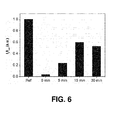
- the remaining substrate 2 not exposed to (NH 4 ) 2 S vapour saw its PL intensity decreasing by more than one order of magnitude compared to the bare native oxide-free InP substrate (see 0 in Fig. 5 and 0 min in Fig. 6 ). This indicates a relatively large defect recombination rate at the InP/Gd 1.4 Al 0.6 O 3 interface.
- the quality of the interface was significantly improved when the InP wafer 2 was exposed to (NH 4 ) 2 S vapor prior to the high-k interfacial layer 3 deposition. A strong correlation was observed between the PL intensity and the vapour exposure time (see Fig. 5 and 6 ). The advantage of using a sulphur comprising compound for the interface quality is demonstrated by this experiment.
- the ratio between the integrated intensity of the InP/Gd 1.4 Al 0.6 O 3 stack (It) and the integrated intensity of the reference sample prior to passivation (Iref) is shown in Fig. 6 .
- the maximum increase was observed after 15 minutes of vapour exposure.
- the integrated intensity corresponded to about 60% of the integrated intensity of the reference substrate.
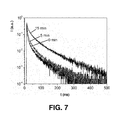
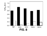
- Fig. 7 shows decay curves for the InP/Gd 1.4 Al 0.6 O 3 stack for 0 min, 5 min and 15 min vapor exposure. It is clear that the lifetime of the minority charge carriers is enhanced when the interface is exposed to sulphur containing compound. From the decay curves the lifetime of the defect recombination and the bandgap emission was extracted and the relative contributions are plotted in Fig. 8 .
- a bare InP substrate is shown as a reference. After deposition of a 4 nm Gd 1.4 Al 0.6 O 3 layer on the oxide free InP substrate (0 min), bandgap emission (white) is reduced and is accompanied by an increase in defect recombination (black). This explains the strong decrease in PL intensity as shown in Fig. 5 .
- the interface quality can be significantly improved by exposure to a sulphur containing compound; the increase in bandgap emission with increasing (NH 4 ) 2 S vapor exposure time was accompanied by a decrease in defect recombination. The trend is comparable to the PL spectra shown in Fig. 5 .
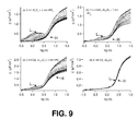
- Fig. 9 (a-c) The impact of Gd content on the electrical properties is shown in Fig. 9 (a-c) for S-passivated n-type InP (5 minutes immersion in (NH 4 ) 2 S solution after 5 minutes native oxide removal in 2M HCl).
- the capacitance is shown as a function of potential for different frequencies. L stands for low frequency (100 Hz) and H stands for high frequency (1 MHz). It is clear that the large frequency dispersion in the lower potential range is decreasing with increasing Gd content. This can be attributed to a decrease in (mid-gap) interface trap density. No clear dependency is observed for the frequency dispersion at larger potentials (i.e. the border trap density is not affected).
- the interface defect density can be further decreased when the n-type InP wafer is exposed for 15 minutes to (NH 4 ) 2 S vapour instead of (NH 4 ) 2 S solution (see Fig. 9 where the frequency dispersion is drastically reduced, Fig. 9d ).
- Interface defect density values as low as ⁇ 1E11 have been observed for the InP/Gd 1.4 Al 0.6 O 3 semiconductor structure 1, which are up to 1 order of magnitude lower than those obtained with immersion in a (NH 4 ) 2 S solution. Also the border trap density is reduced for the vapor based treatment.
- Example 5 Chemical characterization of a semiconductor structure with a 15 min (NH 4 ) 2 S treatment according to an embodiment of the present invention.
- H is a curve corresponding to a simulation assuming a homogeneous distribution of aluminium across the 3 nm thickness of the high-k interfacial layer 3
- S is a curve corresponding to a simulation assuming a nonhomogeneous distribution of Aluminium across the 3 nm thickness of the high-k interfacial layer 3, with Aluminium being concentrated in the top 2 nm of the high-k interfacial layer 3 and absent from the fist nm of the high-k interfacial layer 3
- the E curve is the experimental curve which behave similarly to curve S and suggest that the interface (bottom surface of interfacial layer 3) is poor in Aluminium compared with the top surface of the high-k interfacial layer 3.
- Example 6 electrical characterization of a semiconductor structures 1 comprising an InP substrate 2.
- a 2 inch InP substrate 2 was dipped in a 2M HCl solution for 5 minute in order to remove its native oxide top layer. It was then immersed in a 20 wt% aqueous solution of (NH 4 ) 2 S for 5 minutes. The substrate 2 was then directly transferred into the load lock of an ALD tool and the pressure was decreased from atmospheric pressure to a few torr and then it was backfilled with N 2 until atmospheric pressure. The substrate was then transferred from the load lock to the ALD chamber. The pressure of the ALD chamber was about 3 Torr.
- a Gd x Al y O 3 layer 3 (samples B and C) or a Al 2 O 3 layer (sample A) was then deposited at 250°C by the method of example 1.
- Sample A (comparative) was obtained by performing first a cycle (z), followed by enough cycles (b) to obtain a Al 2 O 3 layer of 2 nm thickness, followed by the ALD deposition of a 2 nm HfO 2 on top of the Al 2 O 3 .
- Sample B was obtained by performing first a cycle (z), followed by alternating Gd cycle (a) and Al cycle (b) until a layer of composition Gd 0.7 Al 1.3 O 3 is obtained with a thickness of 2 nm, followed by the ALD deposition of a 2 nm HfO 2 on top of the Gd 0.7 Al 1.3 O 3 .
- Sample C was obtained by performing first a cycle (z), followed by a number of supercycles, wherein each supercycle comprises four Gd cycles (a) and one Al cycle (b).
- the number of supercycle was adapted to reach a layer of composition G 1.4 Al 0.6 O 3 having a thickness of 2 nm. This was followed by the ALD deposition of a 2 nm HfO 2 on top of the G 1.4 Al 0.6 O 3 .
- the samples were transferred in an anneal oven and an annealing step was performed for 5 minutes at 400°C in a 10% H 2 atmosphere.
- the electrical characterization of the samples A, B and C was then performed by a HP4156C parameter analyzer (see Fig. 2 ).
- the capacitance and parallel conductance were measured for a range of frequencies (between 100Hz and 1MHz). Scanning from room temperature to liquid nitrogen temperatures allowed extracting the distribution of the density of defects at the interface (D, Y-axis) as a function of the bandgap energy of the materials (the X-axis is the energy from the InP valence band edge (eV)).
- the conductance method was used.
- D(E) should typically be evaluated across the device operation range - upper half of the bandgap for a n-FET and lower half of the bandgap for a p-FET.
- the D(E) was evaluated across the upper half of the bandgap.
- the mid-gap Dit values (the values measure at the lowest E value in Fig. 2 ) dropped significantly going from A to C while the near-conduction band Dit values of B and C (the values measured at the highest E value in Fig. 2 ) are getting too low to be extracted accurately ( ⁇ 1E11) and were not plotted.
- the results show significant improvement for samples B and C when compared with the Al 2 O 3 gate stack (A) and the defect density (D) values were below 1 E12 towards the conduction bands (see Fig. 2 ).
- Example 7 electrical characterization of a semiconductor structure 1 comprising an InGaAs substrate 2.
- a 2 inch InGaAs substrate 2 grown by CVD was dipped in a 2M HCl solution for 5 minute in order to remove its native oxide top layer. It was then immersed in a 20 wt% aqueous solution of (NH 4 ) 2 S for 5 minutes.
- the substrate 2 was then directly transferred into the load lock of an ALD tool and the pressure was decreased from atmospheric pressure to a few torr and then it was backfilled with N 2 until atmospheric pressure.
- the substrate was then transferred from the load lock to the ALD chamber.
- the pressure of the ALD chamber was about 3 Torr.
- a GdAlO 3 layer 3 or an Al 2 O 3 layer was then deposited at 250°C by the ALD method of example 1.
- the Al 2 O 3 layer was obtained by performing first a cycle (z), followed by enough cycles (b) to obtain a Al 2 O 3 layer of 2 nm thickness, followed by the ALD deposition of a 2 nm HfO 2 on top of the Al 2 O 3 .
- the GdAlO 3 layer 3 was obtained by performing first a cycle (z), followed by an equal number of Gadolinium (a) and Aluminium (b) cycles.
- the samples were transferred in an anneal oven and an annealing step was performed for 5 minutes at 400°C in a 10% H 2 atmosphere.
- the electrical characterization of the Al 2 O 3 and GdAlO 3 samples was then performed by a HP4156C parameter analyzer.
- the capacitance and parallel conductance were measured at for a range of frequencies (between 100Hz and 1MHz). Scanning from room temperature to liquid nitrogen temperatures allowed extracting the distribution of Dit as a function of the bandgap energy of the materials. For this purpose the conductance method was used.
- the results show significant improvement for GdAlO 3 when compared with the Al 2 O 3 gate stack and the interface defect density (Dit) values were below 1 E12 towards the conduction bands (see Fig. 3 ).
Landscapes
- Insulated Gate Type Field-Effect Transistor (AREA)
- Formation Of Insulating Films (AREA)
Abstract
a. A substrate comprising a III-V material, and
b. A high-k interfacial layer overlaying said substrate,
Wherein said interfacial layer comprises a rare earth aluminate; an n-type FET device comprising the same; and a method for manufacturing the same.
Description
- The present invention relates to the field of semiconductor structures for use in III-V MOS devices, and more specifically to gate stacks for n-FETs.
- The constant drive toward miniaturization of semiconductor devices makes low equivalent oxide thickness dielectrics particularly desirable. The field of III-V MOS devices is no exception. However, when the equivalent oxide thickness is lowered, the tunnelling leakage current trough the dielectric tend to get higher.
- To tackle this problem, high-k dielectrics have been used. However, high-k dielectrics have a small bandgap, which can also contribute to high tunnelling leakage current. Furthermore, the decrease in equivalent oxide thickness should not be accompanied by a decrease in charge mobility in the III-V substrate. Indeed, this mobility is particularly important in Field Effect Transistors.
-
US 2006/0054937 proposes to tackle these issues by inserting between the substrate and the primary dielectric layer an oxide layer including a group III element from the substrate, and by further inserting between said oxide layer and the primary dielectric layer an interfacial dielectric layer. The interfacial dielectric layer includes HfO2, ZrO2, a zirconium silicate alloy, and/or a hafnium silicate alloy. This approach however has the drawbacks of involving a relatively large number of layers, multiplying the chances of defects at the interfaces. Also, the obtained equivalent oxide thickness is relatively large. - For the fabrication of a semi-conductor device comprising a III-V substrate and a high-k dielectric, it would be advantageous to achieve the manufacture of a III-V semiconductor structure enabling:
- a small equivalent oxide thickness for the device,
- a good charge mobility in a region of the III-V substrate, and
- low levels of tunnelling or leakage current through the high-k dielectric.
- To better address one or more of these concerns, in a first aspect of the present invention a semiconductor structure is presented. This semiconductor structure comprises a substrate comprising a III-V material, and an interfacial layer overlaying said substrate. This structure is well suited for further comprising a high-k dielectric layer overlaying said interfacial layer.
- In a first aspect, the present invention relates to a semiconductor structure comprising:
- a. A substrate comprising a III-V material, and
- b. A high-k interfacial layer overlaying said substrate,
- Embodiments of the semiconductor structures of the present invention may present on or more, or even all of the following advantages:
- They may present a large offset between the conduction band of the semi-conductor substrate and the conduction band of the dielectric, thereby permitting a low leakage current, and/or
- They may present a low defect density at the interface between the semi-conductor substrate and the dielectric, thereby permitting a good mobility in a region of the semi-conductor substrate, and/or
- They may present a high dielectric constant for the interfacial layer or for the stack interfacial layer/high-k dielectric layer, thereby permitting a good capacitance and a low leakage current.
- In an embodiment, the substrate comprising a III-V material may have a top surface comprising said III-V material. In this way, the high-k interfacial layer overlaying said substrate will be in physical contact with said III-V material.
- In an embodiment, the substrate comprising a III-V material may be made up entirely from a III-V material.
- As used herein and unless provided otherwise, the term "III-V material" relates to a material comprising or made of a chemical compound with at least one group III (IUPAC group 13) element and at least one group V (IUPAC group 15) element. This includes binary compounds but also higher order compounds such as ternary compounds. It also includes mixture of such compounds.
- Amongst said III-V materials, III-N materials (e.g. GaN) are less preferred. A reason for this is their relatively large bandgaps (>3 eV) making them less suitable for the fabrication of FETs.
- In an embodiment of the first aspect, said III-V material may be selected from InP, InzGa1-zAs and AlzGa1-zAs wherein z is from 0 to 1. These III-V materials typically show a good charge mobility.
- In embodiments, z may preferably be from 0.1 to 1. This is advantageous because it improves charge mobility.
- In embodiments, z may more preferably be from 0.3 to 1. This is advantageous because larger z values lower the conduction band minimum energy level for the III-V material, thereby increasing the conduction band offset between the III-V material and the high-k dielectric layer if present. This in turn reduces the occurrence of leakage current.
- The inventors discovered that the use of a rare earth aluminate for the interfacial layer is particularly advantageous because it results in a low defect density at the interface with an overlaying substrate comprising a III-V material. This defect density is lower than when pure aluminium oxide is overlaying such a substrate. Furthermore, rare earth aluminates are very high-k materials (they have a higher k than pure aluminium oxide for instance).
- In an embodiment, said high-k interfacial layer may be in direct contact with said III-V material.
- In an embodiment, said high-k interfacial layer comprising a rare earth aluminate may be made up entirely of a rare earth aluminate.
- As used herein and unless otherwise specified, the term "high-k" relates to a material exhibiting a permittivity that exceeds the permittivity of silicon dioxide (k= 3.9). Thus, the term "high-k" relates to a relative permittivity of 4 or more unless otherwise specified.
- Rare earth elements are the following elements: Sc, Y, La, Ce, Pr, Nd, Pm, Sm, Eu, Gd, Tb, Dy, Ho, Er, Tm, Yb, and Lu.
- Rare earth aluminates have the following general formula: RExAlyO3 wherein RE is one or more rare earth elements (typically a single rare earth element), wherein x+y = 2 and wherein x is from 0.1 to 1.9, preferably from 0.4 to 1.6. If more than one rare earth is present, x is the sum of the contributions (x1, x2, ...) from each rare earth element.
- The semi-conductor structure comprising only the substrate and the interfacial layer is typically an intermediate structure particularly well suited for being overlaid by a high-k dielectric layer.
- In an embodiment of the first aspect, the semiconductor structure may further comprise a high-k dielectric layer overlying said interfacial layer. This structure is a core structure of several device types and in particular of Field Effect Transistors, wherein a portion of the substrate will serve as a channel and wherein the high-k dielectric layer will serve as a gate dielectric on which a gate electrode can be deposited.
- Typically, the chemical nature of the overlaying high-k dielectric layer is different from the chemical nature of the interfacial layer. This is however not obligatory and in some embodiment, the chemical nature of the interfacial layer and the chemical nature of the high-k dielectric layer may be the same. In some embodiments, an interfacial layer having a relatively large thickness of from 1 to 4 nm could fulfil both functions and serve as both an interfacial layer and a high-k dielectric layer. Typically, the overlaying high-k dielectric layer does not comprise a rare earth aluminate. This is advantageous because rare earth aluminates may have a lower k-value than other high-k dielectric materials (such as HfO2). This is also advantageous because some rare earth aluminates tend to be rather hygroscopic and it is then preferable to cover the top surface of the interfacial layer by a high-k dielectric material, other than a rare earth aluminate, to protect it from water.
- In an embodiment of the first aspect, the high-k dielectric layer may have a higher k value than the interfacial layer.
- In an embodiment of the first aspect, the rare earth aluminate may be selected from GdxAlyO3, ScxAlyO3, and LaxAlyO3, wherein x is from 0.4 to 1.6, preferably from 0.4 to 1.5, more preferably from 0.4 to 1.4, wherein x+y=2.
- Rare earth aluminates in general and the three above compounds in particular are advantageous because they permit to decrease the interface defect density between the III-V substrate and the dielectric.
- GdxAlyO3 is advantageous because it has a relatively high k-value (e.g. about 16 when x=y) permitting a low equivalent oxide thickness.
- ScxAlyO3 is advantageous because it has a low hygroscopy. This permits the use of water in the process for depositing a subsequent high-k dielectric layer. Since such deposition is preferably performed via Atomic Layer Deposition (ALD), the use of H2O as the oxidant has the advantage of avoiding reoxidation of the rare earth aluminate during the subsequent high-k dielectric layer deposition. In an embodiment, of the first aspect, x may be from 0.4 to 1.0. This is sometimes advantageous because values above 1.0 typically gives worse insulating properties and lower band-gap than x values at 1.0 or below. However, x values higher than 1.0 typically give a better interface than x values at or below 1.0. A range of x values from 1.0 to 1.6 may therefore be advantageous for use in high performance devices which can accommodate higher current leakage or for very small equivalent oxide thickness where the charge mobility is more crucial than the amount of leakage. Higher x values increase the k value of the oxides, hence achieving smaller equivalent oxide thickness. An example of a high performance device is an InGaAs channel MOSFET with high Indium content (e.g. 70%). Higher Indium content gives rise to higher drive current and transconductance while the device can tolerate higher gate leakage.
- In an embodiment of the first aspect, x may be from 1.0 to 1.6 while the III-V material is InzGa1-zAs wherein z is from 0.6 to 0.9.
- In an embodiment of the first aspect, when the semiconductor structure further comprises a high-k dielectric layer, the equivalent oxide thickness (EOT) of the stack of the high-k interfacial layer and the high-k dielectric layer may be below 1 nm. This EOT is calculated as follow:

wherein kSiO2 is the k value of SiO2 (i.e. 3.9), tint is the thickness of the interfacial layer, tε is the thickness of the high-k dielectric material, kint is the k value of the interfacial layer, and kε is the k value of the high-k dielectric material. - In an embodiment of the first aspect, the high-k interfacial layer may comprise GdxAlyO3, ScxAlyO3 or LaxAlyO3 wherein x is at least 1.0. This is advantageous because lower x values deteriorate the insulating properties and permits higher current leakages, which is not desired. However, lower x values generally improve the quality of the interface by reducing the defect density. This in turn improves the charge mobility. Therefore, in some embodiments, it is advantageous to have a x value of from 0.4 to 1.0. Below 0.4, the insulating properties are only good enough for few applications.
- In an embodiment of the first aspect, the high-k interfacial layer may comprise GdxAlyO3 wherein x is at least 1.0. This is advantageous because in the case of GdxAlyO3, the increase in interface quality becomes low or even marginal below 1.0.
- In an embodiment of the first aspect, the high-k interfacial layer may comprise ScxAlyO3 wherein x is at most 1.0. This is advantageous because, contrarily to GdxAlyO3, the increase in interface quality below 1.0 remains significant for ScxAlyO3. Furthermore, the insulating properties suffer less than in the case of GdxAlyO3.
- In embodiments of the first aspect where a high-k dielectric layer is present, the high-k dielectric layer may for instance be selected from HfO2, TiO2 and ZnO2. They are advantageous due to their very high k values. Although AlO2 could be used as the high-k dielectric layer, it is less preferred in view of its lower k value.
- In an embodiment of the first aspect, an interface between the substrate and the high-k interfacial layer may have an interface defect density lower than 1013, preferably lower than 7*1012, yet more preferably lower than 5*1012, still more preferably lower than 3*1012, yet still more preferably lower than 2*1012 and most preferably lower than 1.3*1012 defects/cm2 when measured in the middle of the bandgap of the III-V material. For instance, the middle of the bandgap of InP is 1.34 eV/2 = 0.67 eV, and the middle of the bandgap of In0.53Ga0.47As is 0.75 eV/2= 0.38 eV.
- In an embodiment of the first aspect, an interface between the substrate and the high-k interfacial layer may for instance have an interface defect density of from 5*1011 to 1*1013 defects/cm2, preferably from 8*1011 to 7*1012 defects/cm2 when measured in the middle of the bandgap of the III-V material.
- In an embodiment of the first aspect, an interface between the substrate and the high-k interfacial layer may have an interface defect density lower than 5*1012, preferably lower than 3*1012, yet more preferably lower than 1*1012, still more preferably lower than 0.9*1012, yet still more preferably lower than 0.6*1012 and most preferably lower than 0.3*1012 defects/cm2 when measured at at least one energy level within the bandgap of the III-V material. The defect density will typically be lowest at the energy level of the conduction band edge of the III-V material but, due to current instrumental limitations and/or to the low thickness of the RexAlyO3 (<5 nm), an accurate Dit value cannot always be determined accurately at the conduction band edge. In an embodiment of the first aspect, an interface between the substrate and the high-k interfacial layer may have an interface defect density of from 5*1010 to 5.1012 defects/cm2, preferably from 8*1010 to 3*1012 defects/cm2 when measured at at least one energy level within the bandgap of the III-V material.
- This is advantageous because such a low defect density permits a relatively high charge mobility.
- In an embodiment of the first aspect, the high-k interfacial layer may be an incomplete monolayer, a complete monolayer or a multilayer. In embodiments, the thickness of the high-k interfacial layer may be up to 10 nm, preferably up to 6 nm, yet more preferably up to 4 nm and most preferably up to 2 nm. For instance, it can be from 0.5 to 2 nm. A thickness within this range is advantageous as it is thick enough to enable the relatively low defect density. Thicker interfacial layer could be used but it is preferred to limit the thickness of the interfacial layer so that most of the contribution to the equivalent oxide thickness comes from the high-k dielectric layer, which k value can for instance be higher.
- In embodiments of the first aspect where a high-k dielectric layer is present the high-k dielectric layer may be an incomplete monolayer, a complete monolayer or a multilayer. In embodiments, the thickness of the high-k dielectric layer may be up to 10 nm, preferably up to 6 nm, yet more preferably up to 4 nm and most preferably up to 2 nm. For instance, it can be from 0.5 to 4 nm. A thickness within this range is advantageous as it is thick enough to insulate the semiconductor substrate from a gate electrode, when present. Thicker interfacial layer could be used but miniaturization imposes relatively thin dielectric layers. In embodiments, the thickness of the high-k dielectric layer may be from 0.5 to 1.5 times the thickness of the high-k interfacial layer.
- In an embodiment of the first aspect, a leakage current below 0.01 A/cm2 may be achieved at 1 V.
- In an embodiment of the first aspect, a sulphur-comprising compound may be present at the interface between said substrate and said high-k interfacial layer. This sulphur containing compound is preferably inorganic. For instance, said sulphur-comprising compound may be ammonium sulphide. This has the advantage to lower the interface defect density (Dit) and/or to prolong the lifetime of the device.
- In an embodiment, said high-k interfacial layer has a top surface facing away from the substrate and a bottom surface facing said substrate and the aluminium content at the top surface is higher than at the bottom surface. This can for instance be shown by angle resolved X-ray photoelectron spectroscopy (XPS).
- In a second aspect, the present invention relates to a FET device, preferably a n-type FET device comprising a semiconductor structure according to any embodiment of the first aspect.
- Typically, an FET device according to the second aspect may comprise
- A substrate comprising a III-V material, said substrate comprising a source, a drain and a channel region between said source and said drain,
- A high-k interfacial layer overlying said substrate, wherein said interfacial layer comprises a rare earth aluminate,
- A high-k dielectric layer overlying said interfacial layer, and
- A gate electrode overlaying said high-k dielectric layer.
- The substrate, the high-k interfacial layer, and the high-k dielectric layer may be according to any embodiment of the first aspect.
- In embodiments, a sulphur-comprising compound as describe in the first aspect may be present at the interface between said substrate and said high-k interfacial layer.
- In a third aspect, the present invention relates to a method for manufacturing a semiconductor structure according to the first aspect comprising the steps of:
- a) Providing a substrate comprising a III-V material, and
- b) Depositing a high-k interfacial layer overlaying said substrate,
- The step a) of providing a substrate may comprise treating said substrate in order to remove native oxide on a surface thereof. This treatment can for instance be an acid treatment. For instance a HCl treatment.
- In an embodiment of the third aspect, said method may further comprise a step a') of providing a sulphur-comprising compound at the interface between said substrate and said high-k interfacial layer. This step a') is typically performed between step a) and step b) by depositing said sulphur-comprising compound onto said substrate. The deposition of the sulphur-comprising compound can be performed in several ways. It can be performed by immerging the substrate in a solution of the sulphur-comprising compound or it can be performed by exposing the substrate to vapours of the sulphur-comprising compound. Exposing the substrate to vapours of the sulphur-comprising compound can be performed by placing the substrate in the atmosphere of a chamber comprising the sulphur-comprising compound solution and its vapour. It can also be performed by synthesising the sulphur-comprising compound in situ (e.g. by mixing NH3, H2S and H2O, thereby generating ammonium sulphate) in a chamber containing the substrate.
- In an embodiment, in step a'), the substrate is contacted with the sulphur comprising compound for a time period such that after step b), the maximum photoluminescence intensity of the semiconductor structure is at least 20%, preferably at least 40% and more preferably at least 50% of the maximum photoluminescence intensity of the bare substrate free of native oxide layer. The time period can vary in function of several parameters including but not limited to whether the state of the sulphur compound (vapour or liquid solution), the pressure of the atmosphere, the temperature, the chemical nature of the sulphur compound, and its concentration in the vapour or liquid.
- In an embodiment, said time period could be 5 to 30 minutes if the exposure is to vapour of (NH4)2S at 1 atm and room temperature.
- In an embodiment, step b) may be performed by Atomic Layer Deposition (ALD) or by molecular beam epitaxy (MBE). ALD is preferred because it is faster. Furthermore, ALD permits easier obtaining of uniform and conformal layers, which thickness can be controlled at the atomic level.
- Suitable precursors for the synthesis of RExAlyO3 are a RE precursor, an Al precursor and an O precursor.
- Examples of Al precursors are Aluminum tris(2,2,6,6-tetramethyl-3,5-heptanedionate), Triisobutylaluminum, Trimethylaluminum (TMA), and Tris(dimethylamido)aluminum(III). TMA is preferred.
- Examples of Gd precursors are Tris[N,N-Bis(trimethylsilyl)amide]gadolinium(III), Tris(cyclopentadienyl)gadolinium(III), and Tris(tetramethylcyclopentadienyl)gadolinium(III).
- Examples of Sc precursors are Tris[N,N-bis(trimethylsilyl)amide]scandium(III), and Tris(cyclopentadienyl)scandium(III).
- Examples of La precursors are Lanthanum(III) isopropoxide, Tris[N,N-bis(trimethylsilyl)amide]lanthanum(III), Tris(cyclopentadienyl)lanthanum(III), and Tris(tetramethylcyclopentadienyl)lanthanum(III).
- Examples of O precursors are H2O, O2 and O3. H2O is preferred.
- The method may further comprise a step c) of overlying a high-k dielectric layer on the high-k interfacial layer. The high-k dielectric layer is preferably deposited via ALD. HfO2, TiO2 and ZnO2 are examples of suitable high-k dielectric layers.
- In general, carbon-free precursors have the advantage of permitting the formation of high-k dielectric layer showing lower current leakage. However, carbon-comprising precursors have the advantage of requiring lower temperature for deposition than carbon-free precursors, which is good for the III-V substrate. The III-V substrate tend to suffer at temperatures above 300°C. ALD depositions on a III-V substrate is therefore preferably performed at or below 300 °C.
- Examples of Hf precursors are Bis(tert-butylcyclopentadienyl)dimethylhafnium(IV), Bis(methyl-η5-cyclopentadienyl)dimethylhafnium, Bis(methyl-η5-cyclopentadienyl)methoxymethylhafnium, Bis(trimethylsilyl)amidohafnium(IV) chloride, Dimethylbis(cyclopentadienyl)hafnium(IV), Hafnium(IV) tert-butoxide, Hafnium isopropoxide isopropanol adduct, Tetrakis(diethylamido)hafnium(IV), Tetrakis(dimethylamido)hafnium(IV), Hafnium tetrachloride, and Tetrakis(ethylmethylamido)hafnium(IV). Hafnium tetrachloride has the advantage to be carbon-free, permitting a lower leakage current.
- Examples of Ti precursors are Bis(tert-butylcyclopentadienyl)titanium(IV) dichloride, Bis(diethylamido)bis(dimethylamido)titanium(IV), Tetrakis(diethylamido)titanium(IV), Tetrakis(ethylmethylamido)titanium(IV), Titanium(IV) diisopropoxide-bis(2,2,6,6-tetramethyl-3,5-heptanedionate), Titanium(IV) isopropoxide, and Titanium tetrachloride.
- Titanium precursors are advantageous because they permit a better scaling. They however have the drawback of requiring a relatively high deposition temperature. Titanium tetrachloride is advantageous because it is carbon-free, permitting a lower leakage current.
- Examples of Zn precursors are Bis(pentafluorophenyl)zinc, Bis(2,2,6,6-tetramethyl-3,5-heptanedionato)zinc(II), Diethylzinc, and Diphenylzinc.
- Particular and preferred aspects of the invention are set out in the accompanying independent and dependent claims. Features from the dependent claims may be combined with features of the independent claims and with features of other dependent claims as appropriate and not merely as explicitly set out in the claims.
- Although there has been constant improvement, change and evolution of devices in this field, the present concepts are believed to represent substantial new and novel improvements, including departures from prior practices, resulting in the provision of more efficient, stable and reliable devices of this nature.
- The method may further comprise a step d of annealing the semiconductor structure after the deposition of the high k dielectric layer. This annealing is preferably performed in a reductive atmosphere.
- For instance, after the ALD deposition, the sample may be transferred in an anneal oven and an annealing step is performed for 5 minutes at 400°C in a 10% H2 atmosphere.
- The method may further comprise a step e of depositing a top metal gate on the high-k dielectric layer. For instance, a 80nm of TiN may deposited as a top metal gate.
- The above and other characteristics, features and advantages of the present invention will become apparent from the following detailed description, taken in conjunction with the accompanying drawings, which illustrate, by way of example, the principles of the invention. This description is given for the sake of example only, without limiting the scope of the invention. The reference figures quoted below refer to the attached drawings.
-
-
Fig. 1 is a schematic representation of a semiconductor structure according to an embodiment of the present invention. -
Fig. 2 is a graph of the defect density versus the energy from the InP valence band edge for semiconductor structures according to embodiments of the present invention as well as for a comparative semiconductor structure. -
Fig. 3 is a graph of the defect density versus the energy from the InGaAs valence band edge for a semiconductor structure according to an embodiment of the present invention as well as for a comparative semiconductor structure. -
Fig. 4 is a diagram illustrating a method for manufacturing a semiconductor structure according to an embodiment of the present invention. -
Fig. 5 is a graph of the photoluminescence intensity versus the wavelength for semiconductor structures according to embodiments of the present invention and for a bare substrate. -
Fig. 6 shows the integrated intensity ratio between the photoluminescence intensity of a InP/Gd1.4Al0.6O3 semiconductor structure according to embodiments of the present invention and the photoluminescence intensity of a bare InP substrate for various exposure times to (NH4)2S vapour. -
Fig. 7 shows the decay curves for semiconductor structures at different exposure times according to embodiments of the present invention. -
Fig. 8 shows the lifetime contribution of defect recombination or bandgap emission for a bare InP substrate or for embodiments of the present invention at different exposure times to (NH4)2S vapour. -
Fig. 9 shows the capacitance as a function of the gate voltage and the frequency for embodiments of the present invention. -
Fig. 10 shows the normalized Al/Gd synchrotron emission ratio as a function of the photon energy for an embodiment of the present invention and for simulations. - In the different figures, the same reference signs refer to the same or analogous elements.
- The present invention will be described with respect to particular embodiments and with reference to certain drawings but the invention is not limited thereto but only by the claims. The drawings described are only schematic and are non-limiting. In the drawings, the size of some of the elements may be exaggerated and not drawn on scale for illustrative purposes. The dimensions and the relative dimensions do not correspond to actual reductions to practice of the invention.
- Furthermore, the terms first, second, third and the like in the description and in the claims, are used for distinguishing between similar elements and not necessarily for describing a sequence, either temporally, spatially, in ranking or in any other manner. It is to be understood that the terms so used are interchangeable under appropriate circumstances and that the embodiments of the invention described herein are capable of operation in other sequences than described or illustrated herein.
- Moreover, the terms top, bottom, over, under and the like in the description and the claims are used for descriptive purposes and not necessarily for describing relative positions. It is to be understood that the terms so used are interchangeable under appropriate circumstances and that the embodiments of the invention described herein are capable of operation in other orientations than described or illustrated herein.
- It is to be noticed that the term "comprising", used in the claims, should not be interpreted as being restricted to the means listed thereafter; it does not exclude other elements or steps. It is thus to be interpreted as specifying the presence of the stated features, integers, steps or components as referred to, but does not preclude the presence or addition of one or more other features, integers, steps or components, or groups thereof. Thus, the scope of the expression "a device comprising means A and B" should not be limited to devices consisting only of components A and B. It means that with respect to the present invention, the only relevant components of the device are A and B.
- Reference throughout this specification to "one embodiment" or "an embodiment" means that a particular feature, structure or characteristic described in connection with the embodiment is included in at least one embodiment of the present invention. Thus, appearances of the phrases "in one embodiment" or "in an embodiment" in various places throughout this specification are not necessarily all referring to the same embodiment, but may. Furthermore, the particular features, structures or characteristics may be combined in any suitable manner, as would be apparent to one of ordinary skill in the art from this disclosure, in one or more embodiments.
- Similarly it should be appreciated that in the description of exemplary embodiments of the invention, various features of the invention are sometimes grouped together in a single embodiment, figure, or description thereof for the purpose of streamlining the disclosure and aiding in the understanding of one or more of the various inventive aspects. This method of disclosure, however, is not to be interpreted as reflecting an intention that the claimed invention requires more features than are expressly recited in each claim. Rather, as the following claims reflect, inventive aspects lie in less than all features of a single foregoing disclosed embodiment. Thus, the claims following the detailed description are hereby expressly incorporated into this detailed description, with each claim standing on its own as a separate embodiment of this invention.
- Furthermore, while some embodiments described herein include some but not other features included in other embodiments, combinations of features of different embodiments are meant to be within the scope of the invention, and form different embodiments, as would be understood by those in the art. For example, in the following claims, any of the claimed embodiments can be used in any combination.
- Furthermore, some of the embodiments are described herein as a method or combination of elements of a method that can be implemented by a processor of a computer system or by other means of carrying out the function. Thus, a processor with the necessary instructions for carrying out such a method or element of a method forms a means for carrying out the method or element of a method. Furthermore, an element described herein of an apparatus embodiment is an example of a means for carrying out the function performed by the element for the purpose of carrying out the invention.
- In the description provided herein, numerous specific details are set forth. However, it is understood that embodiments of the invention may be practiced without these specific details. In other instances, well-known methods, structures and techniques have not been shown in detail in order not to obscure an understanding of this description.
- The invention will now be described by a detailed description of several embodiments of the invention. It is clear that other embodiments of the invention can be configured according to the knowledge of persons skilled in the art without departing from technical teaching of the invention, the invention being limited only by the terms of the appended claims.
- Reference will be made to transistors. These are three-terminal devices having a first main electrode such as a drain, a second main electrode such as a source and a control electrode such as a gate for controlling the flow of electrical charges between the first and second main electrodes.
- Example 1: Manufacture of a semiconductor structure 1 (see
Fig. 1 ) comprising a GdxAlyO3interfacial layer 3 according to an embodiment of the present invention. - A 2 inch
bulk InP substrate 2 or anInGaAs substrate 2 grown by CVD or MBE on a 2 inch bulk InP substrate is dipped in a 2M HCl solution for 5 minute in order to remove its native oxide top layer. It is then immersed in a 20 wt% aqueous solution of (NH4)2S for 5 minutes. Thesubstrate 2 is then directly transferred into the load lock of an ALD reactor and the pressure is decreased from atmospheric pressure to a few torr and then it is backfilled with N2 until atmospheric pressure. The substrate is then transferred from the load lock to the ALD chamber. The pressure of the ALD chamber is about 3 Torr. A GdxAlyO3 layer 4 is then deposited at 250°C by the method illustrated inFig. 4 . First a water pulse / N2 purge is performed (z) in order to saturate thesubstrate 2 with hydroxyl groups, second one or more Gadolinium deposition cycles (a) are performed. A cycle (a) consists in a Gd precursor (e.g. Gd(iPrCp)3) pulse followed by a N2 purge, followed by an oxidative pulse (typically a water pulse), followed by a N2 purge. Third, one or more aluminium deposition cycles (b) are performed. A cycle (b) consists in an aluminium precursor pulse (typically TMA), followed by a N2 purge, followed by an oxidative pulse (typically a water pulse), followed by a N2 purge. The sum of the one or more Gadolinium deposition cycle (a) plus the one or more Aluminium deposition cycle (b) amounts to one supercycle. The thickness of the GdxAlyO3 layer 3 can be controlled by the number of ALD super cycles while the composition is tuned by the number of cycles (a) and (b). - After the ALD deposition, the sample is transferred in an anneal oven and an annealing step is performed for 5 minutes at 400°C in a 10% H2 atmosphere. 80nm of TiN is deposited as a top metal gate.
- Example 2: Manufacture of a
semiconductor structure 1 comprising a ScxAlyO3interfacial layer 3 according to an embodiment of the present invention. - Example 1 is repeated but a Sc precursor is used instead of a Gd precursor.
- Example 3: Manufacture of a
semiconductor structure 1 comprising a LaxAlyO3interfacial layer 3 according to an embodiment of the present invention. - Example 1 is repeated but a La precursor is used instead of a Gd precursor.
- Example 4: Influence of the presence of a sulphur-comprising compound at the interface between the
substrate 2 and the high-kinterfacial layer 3. - 2 inch
bulk InP substrates 2 were dipped in a 2M HCl solution for 5 minutes in order to remove their native oxide top layer. - The photoluminescence of one of these substrates 2 (the reference substrate) was then measured and is shown in
Fig. 5 (Ref). A high photoluminescence intensity was observed. - The remaining
substrates 2 were then either not exposed to (NH4)2S vapours or exposed to (NH4)2S vapours for a period of from 5 to 30 minutes. In a next step, these remainingsubstrates 2 were coated by ALD with a 4 nm Gd1.4Al0.6O3 layer 3 via an ALD procedure as described in example 1 wherein each supercycle comprises four Gd cycles (a) and one Al cycle (b). - The remaining
substrate 2 not exposed to (NH4)2S vapour, saw its PL intensity decreasing by more than one order of magnitude compared to the bare native oxide-free InP substrate (see 0 inFig. 5 and 0 min inFig. 6 ). This indicates a relatively large defect recombination rate at the InP/Gd1.4Al0.6O3 interface. The quality of the interface was significantly improved when theInP wafer 2 was exposed to (NH4)2S vapor prior to the high-kinterfacial layer 3 deposition. A strong correlation was observed between the PL intensity and the vapour exposure time (seeFig. 5 and6 ). The advantage of using a sulphur comprising compound for the interface quality is demonstrated by this experiment. The ratio between the integrated intensity of the InP/Gd1.4Al0.6O3 stack (It) and the integrated intensity of the reference sample prior to passivation (Iref) is shown inFig. 6 . The maximum increase was observed after 15 minutes of vapour exposure. The integrated intensity corresponded to about 60% of the integrated intensity of the reference substrate. - An analogous experiment was then conducted while substituting Al2O3 for Gd1.4Al0.6O3. Here, no increase in PL intensity was observed after (NH4)2S vapour exposure. An It/I0 ratio of ∼0.1 was observed after 15 minutes of vapour exposure. This provides strong evidence that the combination of a rare earth based
aluminate layer 3 and sulphur is particularly advantageous compared to Al2O3 and sulphur for achieving a high quality interface. -
Fig. 7 shows decay curves for the InP/Gd1.4Al0.6O3 stack for 0 min, 5 min and 15 min vapor exposure. It is clear that the lifetime of the minority charge carriers is enhanced when the interface is exposed to sulphur containing compound. From the decay curves the lifetime of the defect recombination and the bandgap emission was extracted and the relative contributions are plotted inFig. 8 . A bare InP substrate is shown as a reference. After deposition of a 4 nm Gd1.4Al0.6O3 layer on the oxide free InP substrate (0 min), bandgap emission (white) is reduced and is accompanied by an increase in defect recombination (black). This explains the strong decrease in PL intensity as shown inFig. 5 . The interface quality can be significantly improved by exposure to a sulphur containing compound; the increase in bandgap emission with increasing (NH4)2S vapor exposure time was accompanied by a decrease in defect recombination. The trend is comparable to the PL spectra shown inFig. 5 . - The impact of Gd content on the electrical properties is shown in
Fig. 9 (a-c) for S-passivated n-type InP (5 minutes immersion in (NH4)2S solution after 5 minutes native oxide removal in 2M HCl). The capacitance is shown as a function of potential for different frequencies. L stands for low frequency (100 Hz) and H stands for high frequency (1 MHz). It is clear that the large frequency dispersion in the lower potential range is decreasing with increasing Gd content. This can be attributed to a decrease in (mid-gap) interface trap density. No clear dependency is observed for the frequency dispersion at larger potentials (i.e. the border trap density is not affected). The interface defect density can be further decreased when the n-type InP wafer is exposed for 15 minutes to (NH4)2S vapour instead of (NH4)2S solution (seeFig. 9 where the frequency dispersion is drastically reduced,Fig. 9d ). Interface defect density values as low as ∼1E11 have been observed for the InP/Gd1.4Al0.6O3 semiconductor structure 1, which are up to 1 order of magnitude lower than those obtained with immersion in a (NH4)2S solution. Also the border trap density is reduced for the vapor based treatment. An InP/4nm Gd1.4Al0.6O3 structure wherein the InP was immersed for 15 min in (NH4)2S solution (20wt%) (not shown) showed worst results. A InP/2 nm Gd1.4Al0.6O3 structure wherein the InP was exposed for 15 minutes to (NH4)2S vapour showed better photoluminescence (not shown) than the corresponding 4 nm sample but its electrical characteristics could not be measured. - Example 5: Chemical characterization of a semiconductor structure with a 15 min (NH4)2S treatment according to an embodiment of the present invention.
- Synchrotron emission studies performed on a
semiconductor structure 1 comprising aInP substrate 2 treated for 15 min with (NH4)2S vapour and overlaid with 3 nm GdAlO3 layer 3 in a manner analogous to example 1 wherein alternating Gd cycle (a) and Al cycle (b) are used, reveal that Al is preferentially at the surface of the interfacial layer and Gd preferentially at the interface with the substrate (seeFig. 10 ). InFig. 10 , the normalized Al (2p)/Gd (4d) intensity ratio as a function of photon energy is shown inFig. 10 . InFig. 10 , H is a curve corresponding to a simulation assuming a homogeneous distribution of aluminium across the 3 nm thickness of the high-kinterfacial layer 3; S is a curve corresponding to a simulation assuming a nonhomogeneous distribution of Aluminium across the 3 nm thickness of the high-kinterfacial layer 3, with Aluminium being concentrated in the top 2 nm of the high-kinterfacial layer 3 and absent from the fist nm of the high-kinterfacial layer 3; the E curve is the experimental curve which behave similarly to curve S and suggest that the interface (bottom surface of interfacial layer 3) is poor in Aluminium compared with the top surface of the high-kinterfacial layer 3. - Example 6: electrical characterization of a
semiconductor structures 1 comprising anInP substrate 2. - A 2
inch InP substrate 2 was dipped in a 2M HCl solution for 5 minute in order to remove its native oxide top layer. It was then immersed in a 20 wt% aqueous solution of (NH4)2S for 5 minutes. Thesubstrate 2 was then directly transferred into the load lock of an ALD tool and the pressure was decreased from atmospheric pressure to a few torr and then it was backfilled with N2 until atmospheric pressure. The substrate was then transferred from the load lock to the ALD chamber. The pressure of the ALD chamber was about 3 Torr. A GdxAlyO3 layer 3 (samples B and C) or a Al2O3 layer (sample A) was then deposited at 250°C by the method of example 1. - Sample A (comparative) was obtained by performing first a cycle (z), followed by enough cycles (b) to obtain a Al2O3 layer of 2 nm thickness, followed by the ALD deposition of a 2 nm HfO2 on top of the Al2O3.
- Sample B was obtained by performing first a cycle (z), followed by alternating Gd cycle (a) and Al cycle (b) until a layer of composition Gd0.7Al1.3O3 is obtained with a thickness of 2 nm, followed by the ALD deposition of a 2 nm HfO2 on top of the Gd0.7Al1.3O3.
- Sample C was obtained by performing first a cycle (z), followed by a number of supercycles, wherein each supercycle comprises four Gd cycles (a) and one Al cycle (b). The number of supercycle was adapted to reach a layer of composition G1.4Al0.6O3 having a thickness of 2 nm. This was followed by the ALD deposition of a 2 nm HfO2 on top of the G1.4Al0.6O3.
- After the ALD deposition, the samples were transferred in an anneal oven and an annealing step was performed for 5 minutes at 400°C in a 10% H2 atmosphere.
- The electrical characterization of the samples A, B and C was then performed by a HP4156C parameter analyzer (see
Fig. 2 ). The capacitance and parallel conductance were measured for a range of frequencies (between 100Hz and 1MHz). Scanning from room temperature to liquid nitrogen temperatures allowed extracting the distribution of the density of defects at the interface (D, Y-axis) as a function of the bandgap energy of the materials (the X-axis is the energy from the InP valence band edge (eV)). For this purpose the conductance method was used. D(E) should typically be evaluated across the device operation range - upper half of the bandgap for a n-FET and lower half of the bandgap for a p-FET. In the present case, the D(E) was evaluated across the upper half of the bandgap. The mid-gap Dit values (the values measure at the lowest E value inFig. 2 ) dropped significantly going from A to C while the near-conduction band Dit values of B and C (the values measured at the highest E value inFig. 2 ) are getting too low to be extracted accurately (∼1E11) and were not plotted. The results show significant improvement for samples B and C when compared with the Al2O3 gate stack (A) and the defect density (D) values were below 1 E12 towards the conduction bands (seeFig. 2 ). - Example 7: electrical characterization of a
semiconductor structure 1 comprising anInGaAs substrate 2. - A 2
inch InGaAs substrate 2 grown by CVD was dipped in a 2M HCl solution for 5 minute in order to remove its native oxide top layer. It was then immersed in a 20 wt% aqueous solution of (NH4)2S for 5 minutes. Thesubstrate 2 was then directly transferred into the load lock of an ALD tool and the pressure was decreased from atmospheric pressure to a few torr and then it was backfilled with N2 until atmospheric pressure. The substrate was then transferred from the load lock to the ALD chamber. The pressure of the ALD chamber was about 3 Torr. A GdAlO3 layer 3 or an Al2O3 layer was then deposited at 250°C by the ALD method of example 1. - The Al2O3 layer was obtained by performing first a cycle (z), followed by enough cycles (b) to obtain a Al2O3 layer of 2 nm thickness, followed by the ALD deposition of a 2 nm HfO2 on top of the Al2O3.
- The GdAlO3 layer 3 was obtained by performing first a cycle (z), followed by an equal number of Gadolinium (a) and Aluminium (b) cycles.
- After the ALD deposition, the samples were transferred in an anneal oven and an annealing step was performed for 5 minutes at 400°C in a 10% H2 atmosphere.
- The electrical characterization of the Al2O3 and GdAlO3 samples was then performed by a HP4156C parameter analyzer. The capacitance and parallel conductance were measured at for a range of frequencies (between 100Hz and 1MHz). Scanning from room temperature to liquid nitrogen temperatures allowed extracting the distribution of Dit as a function of the bandgap energy of the materials. For this purpose the conductance method was used. The results show significant improvement for GdAlO3 when compared with the Al2O3 gate stack and the interface defect density (Dit) values were below 1 E12 towards the conduction bands (see
Fig. 3 ). - It is to be understood that although preferred embodiments, specific constructions and configurations, as well as materials, have been discussed herein for devices according to the present invention, various changes or modifications in form and detail may be made without departing from the scope and spirit of this invention. For example, any formulas given above are merely representative of procedures that may be used. Functionality may be added or deleted from the block diagrams and operations may be interchanged among functional blocks. Steps may be added or deleted to methods described within the scope of the present invention.
Claims (16)
- A semiconductor structure (1) comprising:a. A substrate (2) comprising a III-V material, andb. A high-k interfacial layer (3) overlaying said substrate (2),Wherein said interfacial layer (3) comprises a rare earth aluminate.
- The semiconductor structure (1) of claim 1, further comprising a high-k dielectric layer (4) overlying said interfacial layer (3).
- The semiconductor structure (1) of any one of the preceding claims, wherein said rare earth aluminate is selected from GdxAlyO3, ScxAlyO3, LaxAlyO3, wherein x is from 0.4 to 1.6, preferably from 0.4 to 1.5, more preferably from 0.4 to 1.4, wherein x+y=2.
- The semiconductor structure (1) of any one of claims 2 to 3, wherein the equivalent oxide thickness of the stack of the high-k interfacial layer (3) and the high-k dielectric layer (4) is below 1 nm.
- The semiconductor structure (1) of any one of the preceding claims, wherein said III-V material is selected from InP, InzGa1-zAs and AlzGa1-z As wherein z is from 0 to1.
- The semiconductor structure (1) of any one of the preceding claims, wherein the high-k interfacial layer (3) comprises GdxAlyO3 wherein x is at most 1.0.
- The semiconductor structure (1) of any one of the preceding claims, wherein the high-k interfacial layer (3) comprises ScxAlyO3 wherein y is at least 0.5.
- The semiconductor structure (1) of any one of claims 2 to 7, wherein said high-k dielectric layer (4) is selected from HfO2, TiO2, and ZnO2.
- The semiconductor structure (1) according to any one of the preceding claims, wherein an interface between the substrate (2) and the high-k interfacial layer (3) has an interface defect density of from 5*1010 to 5*1012 defects/cm2 when measure at at least one energy level within the bandgap of the III-V material.
- The semiconductor structure (1) according to any one of claims 1 to 9, wherein the thickness of the high-k interfacial layer (3) is from 0.5 to 2 nm.
- The semiconductor structure (1) according to any one of claims 2 to 10, wherein the thickness of the high-k dielectric layer (4) is from 0.5 to 2 nm.
- The semiconductor structure (1) according to any one of claims 2 to 11, wherein a leakage current below 0.01 A/cm2 is achieved at 1 V.
- The semiconductor structure (1) according to any one of the preceding claims wherein a sulphur-comprising compound is present at the interface between said substrate (2) and said high-k interfacial layer (3).
- The semiconductor structure (1) according to any one of the preceding claims wherein said high-k interfacial layer (3) has a top surface facing away from the substrate (2) and a bottom surface facing said substrate (2) and wherein the aluminium content at the top surface is higher than at the bottom surface.
- An n-type FET device comprising a semiconductor structure (1) according to any one of the preceding claims.
- A method for manufacturing a semiconductor structure (1) according to claim 1 comprising the steps of:a. Providing a substrate (2) comprising a III-V material, andb. Depositing a high-k interfacial layer (3) overlaying said substrate (2), wherein said interfacial layer (3) comprises a rare earth aluminate.
Priority Applications (4)
| Application Number | Priority Date | Filing Date | Title |
|---|---|---|---|
| EP13177959.7A EP2830096B1 (en) | 2013-07-25 | 2013-07-25 | III-V semiconductor device with interfacial layer |
| TW103125044A TWI612564B (en) | 2013-07-25 | 2014-07-22 | Three-five semiconductors with interface layers |
| KR1020140094252A KR20150013065A (en) | 2013-07-25 | 2014-07-24 | Iii-v semiconductor device with interfacial layer |
| US14/341,629 US9691872B2 (en) | 2013-07-25 | 2014-07-25 | III-V semiconductor device with interfacial layer |
Applications Claiming Priority (1)
| Application Number | Priority Date | Filing Date | Title |
|---|---|---|---|
| EP13177959.7A EP2830096B1 (en) | 2013-07-25 | 2013-07-25 | III-V semiconductor device with interfacial layer |
Publications (2)
| Publication Number | Publication Date |
|---|---|
| EP2830096A1 true EP2830096A1 (en) | 2015-01-28 |
| EP2830096B1 EP2830096B1 (en) | 2016-04-13 |
Family
ID=48874870
Family Applications (1)
| Application Number | Title | Priority Date | Filing Date |
|---|---|---|---|
| EP13177959.7A Active EP2830096B1 (en) | 2013-07-25 | 2013-07-25 | III-V semiconductor device with interfacial layer |
Country Status (4)
| Country | Link |
|---|---|
| US (1) | US9691872B2 (en) |
| EP (1) | EP2830096B1 (en) |
| KR (1) | KR20150013065A (en) |
| TW (1) | TWI612564B (en) |
Families Citing this family (5)
| Publication number | Priority date | Publication date | Assignee | Title |
|---|---|---|---|---|
| US9799747B2 (en) * | 2015-03-12 | 2017-10-24 | International Business Machines Corporation | Low resistance contact for semiconductor devices |
| CN105097901B (en) * | 2015-07-16 | 2018-05-08 | 中国科学院微电子研究所 | Composite gate dielectric layer applied to III-V substrate and manufacturing method thereof |
| US10008580B2 (en) * | 2016-03-21 | 2018-06-26 | Samsung Electronics Co., Ltd. | FET including an InGaAs channel and method of enhancing performance of the FET |
| CN109148571B (en) * | 2018-09-07 | 2021-03-02 | 北京大学 | A novel high-k gate dielectric composite film and preparation method thereof |
| KR20220071114A (en) * | 2020-11-23 | 2022-05-31 | 에이에스엠 아이피 홀딩 비.브이. | Method of forming structures for threshold voltage control |
Citations (2)
| Publication number | Priority date | Publication date | Assignee | Title |
|---|---|---|---|---|
| US20060054937A1 (en) | 2004-09-10 | 2006-03-16 | Gerald Lucovsky | Semiconductor devices having an interfacial dielectric layer and related methods |
| WO2007146859A1 (en) * | 2006-06-12 | 2007-12-21 | Osemi, Inc. | Integrated transistor devices |
Family Cites Families (9)
| Publication number | Priority date | Publication date | Assignee | Title |
|---|---|---|---|---|
| AU2003217189A1 (en) | 2002-01-22 | 2003-09-02 | Massachusetts Institute Of Technology | A method of fabrication for iii-v semiconductor surface passivation |
| EP1634323A4 (en) * | 2003-06-13 | 2008-06-04 | Univ North Carolina State | COMPLEX OXIDES FOR USE IN SEMICONDUCTOR DEVICES AND ASSOCIATED METHODS |
| US7759746B2 (en) | 2006-03-31 | 2010-07-20 | Tokyo Electron Limited | Semiconductor device with gate dielectric containing aluminum and mixed rare earth elements |
| US7816737B2 (en) | 2006-03-31 | 2010-10-19 | Tokyo Electron Limited | Semiconductor device with gate dielectric containing mixed rare earth elements |
| US20080003752A1 (en) | 2006-06-30 | 2008-01-03 | Metz Matthew V | Gate dielectric materials for group III-V enhancement mode transistors |
| US7834426B2 (en) | 2007-06-29 | 2010-11-16 | Intel Corporation | High-k dual dielectric stack |
| EP2337064B1 (en) * | 2009-12-18 | 2014-08-06 | Imec | Dielectric layer for flash memory device and method for manufacturing thereof |
| US8227833B2 (en) | 2009-12-23 | 2012-07-24 | Intel Corporation | Dual layer gate dielectrics for non-silicon semiconductor devices |
| US8575653B2 (en) | 2010-09-24 | 2013-11-05 | Intel Corporation | Non-planar quantum well device having interfacial layer and method of forming same |
-
2013
- 2013-07-25 EP EP13177959.7A patent/EP2830096B1/en active Active
-
2014
- 2014-07-22 TW TW103125044A patent/TWI612564B/en active
- 2014-07-24 KR KR1020140094252A patent/KR20150013065A/en not_active Withdrawn
- 2014-07-25 US US14/341,629 patent/US9691872B2/en active Active
Patent Citations (2)
| Publication number | Priority date | Publication date | Assignee | Title |
|---|---|---|---|---|
| US20060054937A1 (en) | 2004-09-10 | 2006-03-16 | Gerald Lucovsky | Semiconductor devices having an interfacial dielectric layer and related methods |
| WO2007146859A1 (en) * | 2006-06-12 | 2007-12-21 | Osemi, Inc. | Integrated transistor devices |
Non-Patent Citations (4)
| Title |
|---|
| HUANG J ET AL: "InGaAs MOSFET performance and reliability improvement by simultaneous reduction of oxide and interface charge in ALD (La)AlOx/ZrO2 gate stack", ELECTRON DEVICES MEETING (IEDM), 2009 IEEE INTERNATIONAL, IEEE, PISCATAWAY, NJ, USA, 7 December 2009 (2009-12-07), pages 1 - 4, XP031644539, ISBN: 978-1-4244-5639-0 * |
| SHIU K ET AL: "1nm equivalent oxide thickness in Ga2O3(Gd2O3)â In0.2Ga0.8As metal-oxide-semiconductor capacitors", APPLIED PHYSICS LETTERS, AMERICAN INSTITUTE OF PHYSICS, US, vol. 92, no. 17, 30 April 2008 (2008-04-30), pages 172904 - 172904, XP012106695, ISSN: 0003-6951, DOI: 10.1063/1.2918835 * |
| Y. WANG ET AL: "MOSFETs on InP Substrate with LaAlO3/HfO2 Bilayer of Different LaAlO3 Thickness and Single LaXAl1-XO Layer with Different La Doping Level", ECS TRANSACTIONS, vol. 50, no. 4, 15 March 2013 (2013-03-15), pages 151 - 156, XP055108781, ISSN: 1938-6737, DOI: 10.1149/05004.0151ecst * |
| ZHAO H ET AL: "HfO2-based In0.53Ga0.47As MOSFETs (EOTâ 10Ã ) using various interfacial dielectric layers", DEVICE RESEARCH CONFERENCE, 2009. DRC 2009, IEEE, PISCATAWAY, NJ, USA, 22 June 2009 (2009-06-22), pages 89 - 90, XP031581211, ISBN: 978-1-4244-3528-9 * |
Also Published As
| Publication number | Publication date |
|---|---|
| TWI612564B (en) | 2018-01-21 |
| TW201515072A (en) | 2015-04-16 |
| US20150028428A1 (en) | 2015-01-29 |
| EP2830096B1 (en) | 2016-04-13 |
| US9691872B2 (en) | 2017-06-27 |
| KR20150013065A (en) | 2015-02-04 |
Similar Documents
| Publication | Publication Date | Title |
|---|---|---|
| Kim et al. | Characteristics of ZrO 2 gate dielectric deposited using Zr t–butoxide and Zr (NEt 2) 4 precursors by plasma enhanced atomic layer deposition method | |
| Bersuker et al. | Interfacial layer-induced mobility degradation in high-k transistors | |
| US9691872B2 (en) | III-V semiconductor device with interfacial layer | |
| KR20160098322A (en) | Sulfur-containing thin films | |
| Lee et al. | Hafnium oxide gate stack prepared by in situ rapid thermal chemical vapor deposition process for advanced gate dielectrics | |
| Cho et al. | High-k properties of atomic-layer-deposited HfO 2 films using a nitrogen-containing Hf [N (CH 3) 2] 4 precursor and H 2 O oxidant | |
| Gao et al. | Modification of electrical properties and carrier transportation mechanism of ALD-derived HfO2/Si gate stacks by Al2O3 incorporation | |
| Stoklas et al. | Characterization of interface states in AlGaN/GaN metal-oxide-semiconductor heterostructure field-effect transistors with HfO2 gate dielectric grown by atomic layer deposition | |
| Xie et al. | High mobility high-k/Ge pMOSFETs with 1 nm EOT-new concept on interface engineering and interface characterization | |
| Zhao et al. | Advanced CMOS gate stack: Present research progress | |
| Shibata et al. | Effects of carbon impurity in ALD-Al2O3 film on HAXPES spectrum and electrical properties of Al2O3/AlGaN/GaN MIS structure | |
| Rocha et al. | Impact of post-deposition anneal on ALD Al2O3/etched GaN interface for gate-first MOSc-HEMT | |
| Hinkle et al. | Surface studies of III-V materials: oxidation control and device implications | |
| Fan et al. | Effect of post-deposition annealing on the interfacial chemical bonding states and band alignment of atomic layer deposited neodymium oxide on silicon | |
| US9780172B2 (en) | Method of removing oxide from substrate and method of manufacturing semiconductor device using the same | |
| Pampillón et al. | High-k gadolinium scandate on Si obtained by high pressure sputtering from metal targets and in-situ plasma oxidation | |
| Houssa et al. | Experimental and theoretical study of Ge surface passivation | |
| Xu et al. | Plasma enhanced atomic layer deposition of HfO2 with in situ plasma treatment | |
| KR102350688B1 (en) | Field effect transistor and method of fabricating thereof | |
| Feijoo et al. | Gadolinium scandate by high-pressure sputtering for future generations of high-κ dielectrics | |
| Akazawa et al. | Control of plasma-CVD SiO2/InAlN interface by ultrathin atomic-layer-deposited Al2O3 interlayer | |
| Boubenia et al. | Influence of substrate biasing on structural, chemical and electrical properties of Al2O3 thin films deposited by PEALD | |
| Cao et al. | Properties of HfAlO film deposited by plasma enhanced atomic layer deposition | |
| Kang et al. | Effects of remote plasma pre-oxidation of Si substrates on the characteristics of ALD-deposited HfO2 gate dielectrics | |
| Kim et al. | Effect of buffer layer for HfO2 gate dielectrics grown by remote plasma atomic layer deposition |
Legal Events
| Date | Code | Title | Description |
|---|---|---|---|
| 17P | Request for examination filed |
Effective date: 20130725 |
|
| AK | Designated contracting states |
Kind code of ref document: A1 Designated state(s): AL AT BE BG CH CY CZ DE DK EE ES FI FR GB GR HR HU IE IS IT LI LT LU LV MC MK MT NL NO PL PT RO RS SE SI SK SM TR |
|
| AX | Request for extension of the european patent |
Extension state: BA ME |
|
| PUAI | Public reference made under article 153(3) epc to a published international application that has entered the european phase |
Free format text: ORIGINAL CODE: 0009012 |
|
| R17P | Request for examination filed (corrected) |
Effective date: 20150723 |
|
| RBV | Designated contracting states (corrected) |
Designated state(s): AL AT BE BG CH CY CZ DE DK EE ES FI FR GB GR HR HU IE IS IT LI LT LU LV MC MK MT NL NO PL PT RO RS SE SI SK SM TR |
|
| GRAP | Despatch of communication of intention to grant a patent |
Free format text: ORIGINAL CODE: EPIDOSNIGR1 |
|
| RIC1 | Information provided on ipc code assigned before grant |
Ipc: H01L 29/20 20060101ALN20150916BHEP Ipc: H01L 21/28 20060101ALI20150916BHEP Ipc: H01L 29/51 20060101AFI20150916BHEP |
|
| RIC1 | Information provided on ipc code assigned before grant |
Ipc: H01L 29/20 20060101ALN20150924BHEP Ipc: H01L 21/28 20060101ALI20150924BHEP Ipc: H01L 29/51 20060101AFI20150924BHEP |
|
| INTG | Intention to grant announced |
Effective date: 20151015 |
|
| GRAS | Grant fee paid |
Free format text: ORIGINAL CODE: EPIDOSNIGR3 |
|
| GRAA | (expected) grant |
Free format text: ORIGINAL CODE: 0009210 |
|
| AK | Designated contracting states |
Kind code of ref document: B1 Designated state(s): AL AT BE BG CH CY CZ DE DK EE ES FI FR GB GR HR HU IE IS IT LI LT LU LV MC MK MT NL NO PL PT RO RS SE SI SK SM TR |
|
| REG | Reference to a national code |
Ref country code: GB Ref legal event code: FG4D |
|
| REG | Reference to a national code |
Ref country code: AT Ref legal event code: REF Ref document number: 790971 Country of ref document: AT Kind code of ref document: T Effective date: 20160415 Ref country code: CH Ref legal event code: EP |
|
| REG | Reference to a national code |
Ref country code: IE Ref legal event code: FG4D |
|
| REG | Reference to a national code |
Ref country code: DE Ref legal event code: R096 Ref document number: 602013006426 Country of ref document: DE |
|
| REG | Reference to a national code |
Ref country code: FR Ref legal event code: PLFP Year of fee payment: 4 |
|
| REG | Reference to a national code |
Ref country code: LT Ref legal event code: MG4D |
|
| REG | Reference to a national code |
Ref country code: AT Ref legal event code: MK05 Ref document number: 790971 Country of ref document: AT Kind code of ref document: T Effective date: 20160413 |
|
| REG | Reference to a national code |
Ref country code: NL Ref legal event code: MP Effective date: 20160413 |
|
| PG25 | Lapsed in a contracting state [announced via postgrant information from national office to epo] |
Ref country code: LT Free format text: LAPSE BECAUSE OF FAILURE TO SUBMIT A TRANSLATION OF THE DESCRIPTION OR TO PAY THE FEE WITHIN THE PRESCRIBED TIME-LIMIT Effective date: 20160413 Ref country code: FI Free format text: LAPSE BECAUSE OF FAILURE TO SUBMIT A TRANSLATION OF THE DESCRIPTION OR TO PAY THE FEE WITHIN THE PRESCRIBED TIME-LIMIT Effective date: 20160413 Ref country code: NO Free format text: LAPSE BECAUSE OF FAILURE TO SUBMIT A TRANSLATION OF THE DESCRIPTION OR TO PAY THE FEE WITHIN THE PRESCRIBED TIME-LIMIT Effective date: 20160713 Ref country code: NL Free format text: LAPSE BECAUSE OF FAILURE TO SUBMIT A TRANSLATION OF THE DESCRIPTION OR TO PAY THE FEE WITHIN THE PRESCRIBED TIME-LIMIT Effective date: 20160413 Ref country code: PL Free format text: LAPSE BECAUSE OF FAILURE TO SUBMIT A TRANSLATION OF THE DESCRIPTION OR TO PAY THE FEE WITHIN THE PRESCRIBED TIME-LIMIT Effective date: 20160413 |
|
| PG25 | Lapsed in a contracting state [announced via postgrant information from national office to epo] |
Ref country code: LV Free format text: LAPSE BECAUSE OF FAILURE TO SUBMIT A TRANSLATION OF THE DESCRIPTION OR TO PAY THE FEE WITHIN THE PRESCRIBED TIME-LIMIT Effective date: 20160413 Ref country code: ES Free format text: LAPSE BECAUSE OF FAILURE TO SUBMIT A TRANSLATION OF THE DESCRIPTION OR TO PAY THE FEE WITHIN THE PRESCRIBED TIME-LIMIT Effective date: 20160413 Ref country code: GR Free format text: LAPSE BECAUSE OF FAILURE TO SUBMIT A TRANSLATION OF THE DESCRIPTION OR TO PAY THE FEE WITHIN THE PRESCRIBED TIME-LIMIT Effective date: 20160714 Ref country code: RS Free format text: LAPSE BECAUSE OF FAILURE TO SUBMIT A TRANSLATION OF THE DESCRIPTION OR TO PAY THE FEE WITHIN THE PRESCRIBED TIME-LIMIT Effective date: 20160413 Ref country code: SE Free format text: LAPSE BECAUSE OF FAILURE TO SUBMIT A TRANSLATION OF THE DESCRIPTION OR TO PAY THE FEE WITHIN THE PRESCRIBED TIME-LIMIT Effective date: 20160413 Ref country code: AT Free format text: LAPSE BECAUSE OF FAILURE TO SUBMIT A TRANSLATION OF THE DESCRIPTION OR TO PAY THE FEE WITHIN THE PRESCRIBED TIME-LIMIT Effective date: 20160413 Ref country code: PT Free format text: LAPSE BECAUSE OF FAILURE TO SUBMIT A TRANSLATION OF THE DESCRIPTION OR TO PAY THE FEE WITHIN THE PRESCRIBED TIME-LIMIT Effective date: 20160816 Ref country code: HR Free format text: LAPSE BECAUSE OF FAILURE TO SUBMIT A TRANSLATION OF THE DESCRIPTION OR TO PAY THE FEE WITHIN THE PRESCRIBED TIME-LIMIT Effective date: 20160413 |
|
| PG25 | Lapsed in a contracting state [announced via postgrant information from national office to epo] |
Ref country code: IT Free format text: LAPSE BECAUSE OF FAILURE TO SUBMIT A TRANSLATION OF THE DESCRIPTION OR TO PAY THE FEE WITHIN THE PRESCRIBED TIME-LIMIT Effective date: 20160413 Ref country code: BE Free format text: LAPSE BECAUSE OF FAILURE TO SUBMIT A TRANSLATION OF THE DESCRIPTION OR TO PAY THE FEE WITHIN THE PRESCRIBED TIME-LIMIT Effective date: 20160413 |
|
| REG | Reference to a national code |
Ref country code: DE Ref legal event code: R097 Ref document number: 602013006426 Country of ref document: DE |
|
| PG25 | Lapsed in a contracting state [announced via postgrant information from national office to epo] |
Ref country code: EE Free format text: LAPSE BECAUSE OF FAILURE TO SUBMIT A TRANSLATION OF THE DESCRIPTION OR TO PAY THE FEE WITHIN THE PRESCRIBED TIME-LIMIT Effective date: 20160413 Ref country code: SK Free format text: LAPSE BECAUSE OF FAILURE TO SUBMIT A TRANSLATION OF THE DESCRIPTION OR TO PAY THE FEE WITHIN THE PRESCRIBED TIME-LIMIT Effective date: 20160413 Ref country code: DK Free format text: LAPSE BECAUSE OF FAILURE TO SUBMIT A TRANSLATION OF THE DESCRIPTION OR TO PAY THE FEE WITHIN THE PRESCRIBED TIME-LIMIT Effective date: 20160413 Ref country code: CZ Free format text: LAPSE BECAUSE OF FAILURE TO SUBMIT A TRANSLATION OF THE DESCRIPTION OR TO PAY THE FEE WITHIN THE PRESCRIBED TIME-LIMIT Effective date: 20160413 Ref country code: RO Free format text: LAPSE BECAUSE OF FAILURE TO SUBMIT A TRANSLATION OF THE DESCRIPTION OR TO PAY THE FEE WITHIN THE PRESCRIBED TIME-LIMIT Effective date: 20160413 |
|
| PLBE | No opposition filed within time limit |
Free format text: ORIGINAL CODE: 0009261 |
|
| STAA | Information on the status of an ep patent application or granted ep patent |
Free format text: STATUS: NO OPPOSITION FILED WITHIN TIME LIMIT |
|
| PG25 | Lapsed in a contracting state [announced via postgrant information from national office to epo] |
Ref country code: SM Free format text: LAPSE BECAUSE OF FAILURE TO SUBMIT A TRANSLATION OF THE DESCRIPTION OR TO PAY THE FEE WITHIN THE PRESCRIBED TIME-LIMIT Effective date: 20160413 |
|
| REG | Reference to a national code |
Ref country code: CH Ref legal event code: PL |
|
| 26N | No opposition filed |
Effective date: 20170116 |
|
| PG25 | Lapsed in a contracting state [announced via postgrant information from national office to epo] |
Ref country code: MC Free format text: LAPSE BECAUSE OF FAILURE TO SUBMIT A TRANSLATION OF THE DESCRIPTION OR TO PAY THE FEE WITHIN THE PRESCRIBED TIME-LIMIT Effective date: 20160413 |
|
| PG25 | Lapsed in a contracting state [announced via postgrant information from national office to epo] |
Ref country code: CH Free format text: LAPSE BECAUSE OF NON-PAYMENT OF DUE FEES Effective date: 20160731 Ref country code: LI Free format text: LAPSE BECAUSE OF NON-PAYMENT OF DUE FEES Effective date: 20160731 |
|
| REG | Reference to a national code |
Ref country code: IE Ref legal event code: MM4A |
|
| PG25 | Lapsed in a contracting state [announced via postgrant information from national office to epo] |
Ref country code: SI Free format text: LAPSE BECAUSE OF FAILURE TO SUBMIT A TRANSLATION OF THE DESCRIPTION OR TO PAY THE FEE WITHIN THE PRESCRIBED TIME-LIMIT Effective date: 20160413 |
|
| REG | Reference to a national code |
Ref country code: FR Ref legal event code: PLFP Year of fee payment: 5 |
|
| PG25 | Lapsed in a contracting state [announced via postgrant information from national office to epo] |
Ref country code: IE Free format text: LAPSE BECAUSE OF NON-PAYMENT OF DUE FEES Effective date: 20160725 |
|
| PG25 | Lapsed in a contracting state [announced via postgrant information from national office to epo] |
Ref country code: LU Free format text: LAPSE BECAUSE OF NON-PAYMENT OF DUE FEES Effective date: 20160725 |
|
| GBPC | Gb: european patent ceased through non-payment of renewal fee |
Effective date: 20170725 |
|
| PG25 | Lapsed in a contracting state [announced via postgrant information from national office to epo] |
Ref country code: GB Free format text: LAPSE BECAUSE OF NON-PAYMENT OF DUE FEES Effective date: 20170725 |
|
| PG25 | Lapsed in a contracting state [announced via postgrant information from national office to epo] |
Ref country code: HU Free format text: LAPSE BECAUSE OF FAILURE TO SUBMIT A TRANSLATION OF THE DESCRIPTION OR TO PAY THE FEE WITHIN THE PRESCRIBED TIME-LIMIT; INVALID AB INITIO Effective date: 20130725 |
|
| REG | Reference to a national code |
Ref country code: FR Ref legal event code: PLFP Year of fee payment: 6 |
|
| PG25 | Lapsed in a contracting state [announced via postgrant information from national office to epo] |
Ref country code: IS Free format text: LAPSE BECAUSE OF FAILURE TO SUBMIT A TRANSLATION OF THE DESCRIPTION OR TO PAY THE FEE WITHIN THE PRESCRIBED TIME-LIMIT Effective date: 20160413 Ref country code: MK Free format text: LAPSE BECAUSE OF FAILURE TO SUBMIT A TRANSLATION OF THE DESCRIPTION OR TO PAY THE FEE WITHIN THE PRESCRIBED TIME-LIMIT Effective date: 20160413 Ref country code: CY Free format text: LAPSE BECAUSE OF FAILURE TO SUBMIT A TRANSLATION OF THE DESCRIPTION OR TO PAY THE FEE WITHIN THE PRESCRIBED TIME-LIMIT Effective date: 20160413 Ref country code: MT Free format text: LAPSE BECAUSE OF NON-PAYMENT OF DUE FEES Effective date: 20160731 |
|
| PG25 | Lapsed in a contracting state [announced via postgrant information from national office to epo] |
Ref country code: BG Free format text: LAPSE BECAUSE OF FAILURE TO SUBMIT A TRANSLATION OF THE DESCRIPTION OR TO PAY THE FEE WITHIN THE PRESCRIBED TIME-LIMIT Effective date: 20160413 |
|
| PG25 | Lapsed in a contracting state [announced via postgrant information from national office to epo] |
Ref country code: TR Free format text: LAPSE BECAUSE OF FAILURE TO SUBMIT A TRANSLATION OF THE DESCRIPTION OR TO PAY THE FEE WITHIN THE PRESCRIBED TIME-LIMIT Effective date: 20160413 Ref country code: AL Free format text: LAPSE BECAUSE OF FAILURE TO SUBMIT A TRANSLATION OF THE DESCRIPTION OR TO PAY THE FEE WITHIN THE PRESCRIBED TIME-LIMIT Effective date: 20160413 |
|
| P01 | Opt-out of the competence of the unified patent court (upc) registered |
Effective date: 20230513 |
|
| REG | Reference to a national code |
Ref country code: DE Ref legal event code: R079 Ref document number: 602013006426 Country of ref document: DE Free format text: PREVIOUS MAIN CLASS: H01L0029510000 Ipc: H10D0064680000 |
|
| PGFP | Annual fee paid to national office [announced via postgrant information from national office to epo] |
Ref country code: DE Payment date: 20250620 Year of fee payment: 13 |
|
| PGFP | Annual fee paid to national office [announced via postgrant information from national office to epo] |
Ref country code: FR Payment date: 20260619 Year of fee payment: 14 |