EP2829906A1 - Carrier-depletion based silicon waveguide resonant cavity modulator with integrated optical power monitor - Google Patents
Carrier-depletion based silicon waveguide resonant cavity modulator with integrated optical power monitor Download PDFInfo
- Publication number
- EP2829906A1 EP2829906A1 EP14172997.0A EP14172997A EP2829906A1 EP 2829906 A1 EP2829906 A1 EP 2829906A1 EP 14172997 A EP14172997 A EP 14172997A EP 2829906 A1 EP2829906 A1 EP 2829906A1
- Authority
- EP
- European Patent Office
- Prior art keywords
- resonant cavity
- region
- carrier
- type
- silicon waveguide
- Prior art date
- Legal status (The legal status is an assumption and is not a legal conclusion. Google has not performed a legal analysis and makes no representation as to the accuracy of the status listed.)
- Granted
Links
Images


Classifications
-
- G—PHYSICS
- G02—OPTICS
- G02F—OPTICAL DEVICES OR ARRANGEMENTS FOR THE CONTROL OF LIGHT BY MODIFICATION OF THE OPTICAL PROPERTIES OF THE MEDIA OF THE ELEMENTS INVOLVED THEREIN; NON-LINEAR OPTICS; FREQUENCY-CHANGING OF LIGHT; OPTICAL LOGIC ELEMENTS; OPTICAL ANALOGUE/DIGITAL CONVERTERS
- G02F1/00—Devices or arrangements for the control of the intensity, colour, phase, polarisation or direction of light arriving from an independent light source, e.g. switching, gating or modulating; Non-linear optics
- G02F1/01—Devices or arrangements for the control of the intensity, colour, phase, polarisation or direction of light arriving from an independent light source, e.g. switching, gating or modulating; Non-linear optics for the control of the intensity, phase, polarisation or colour
- G02F1/015—Devices or arrangements for the control of the intensity, colour, phase, polarisation or direction of light arriving from an independent light source, e.g. switching, gating or modulating; Non-linear optics for the control of the intensity, phase, polarisation or colour based on semiconductor elements having potential barriers, e.g. having a PN or PIN junction
- G02F1/025—Devices or arrangements for the control of the intensity, colour, phase, polarisation or direction of light arriving from an independent light source, e.g. switching, gating or modulating; Non-linear optics for the control of the intensity, phase, polarisation or colour based on semiconductor elements having potential barriers, e.g. having a PN or PIN junction in an optical waveguide structure
-
- G—PHYSICS
- G02—OPTICS
- G02F—OPTICAL DEVICES OR ARRANGEMENTS FOR THE CONTROL OF LIGHT BY MODIFICATION OF THE OPTICAL PROPERTIES OF THE MEDIA OF THE ELEMENTS INVOLVED THEREIN; NON-LINEAR OPTICS; FREQUENCY-CHANGING OF LIGHT; OPTICAL LOGIC ELEMENTS; OPTICAL ANALOGUE/DIGITAL CONVERTERS
- G02F1/00—Devices or arrangements for the control of the intensity, colour, phase, polarisation or direction of light arriving from an independent light source, e.g. switching, gating or modulating; Non-linear optics
- G02F1/01—Devices or arrangements for the control of the intensity, colour, phase, polarisation or direction of light arriving from an independent light source, e.g. switching, gating or modulating; Non-linear optics for the control of the intensity, phase, polarisation or colour
- G02F1/0121—Operation of devices; Circuit arrangements, not otherwise provided for in this subclass
-
- G—PHYSICS
- G02—OPTICS
- G02F—OPTICAL DEVICES OR ARRANGEMENTS FOR THE CONTROL OF LIGHT BY MODIFICATION OF THE OPTICAL PROPERTIES OF THE MEDIA OF THE ELEMENTS INVOLVED THEREIN; NON-LINEAR OPTICS; FREQUENCY-CHANGING OF LIGHT; OPTICAL LOGIC ELEMENTS; OPTICAL ANALOGUE/DIGITAL CONVERTERS
- G02F1/00—Devices or arrangements for the control of the intensity, colour, phase, polarisation or direction of light arriving from an independent light source, e.g. switching, gating or modulating; Non-linear optics
- G02F1/29—Devices or arrangements for the control of the intensity, colour, phase, polarisation or direction of light arriving from an independent light source, e.g. switching, gating or modulating; Non-linear optics for the control of the position or the direction of light beams, i.e. deflection
- G02F1/31—Digital deflection, i.e. optical switching
- G02F1/313—Digital deflection, i.e. optical switching in an optical waveguide structure
- G02F1/3132—Digital deflection, i.e. optical switching in an optical waveguide structure of directional coupler type
-
- G—PHYSICS
- G02—OPTICS
- G02F—OPTICAL DEVICES OR ARRANGEMENTS FOR THE CONTROL OF LIGHT BY MODIFICATION OF THE OPTICAL PROPERTIES OF THE MEDIA OF THE ELEMENTS INVOLVED THEREIN; NON-LINEAR OPTICS; FREQUENCY-CHANGING OF LIGHT; OPTICAL LOGIC ELEMENTS; OPTICAL ANALOGUE/DIGITAL CONVERTERS
- G02F1/00—Devices or arrangements for the control of the intensity, colour, phase, polarisation or direction of light arriving from an independent light source, e.g. switching, gating or modulating; Non-linear optics
- G02F1/29—Devices or arrangements for the control of the intensity, colour, phase, polarisation or direction of light arriving from an independent light source, e.g. switching, gating or modulating; Non-linear optics for the control of the position or the direction of light beams, i.e. deflection
- G02F1/31—Digital deflection, i.e. optical switching
- G02F1/313—Digital deflection, i.e. optical switching in an optical waveguide structure
- G02F1/3132—Digital deflection, i.e. optical switching in an optical waveguide structure of directional coupler type
- G02F1/3133—Digital deflection, i.e. optical switching in an optical waveguide structure of directional coupler type the optical waveguides being made of semiconducting materials
-
- G—PHYSICS
- G02—OPTICS
- G02F—OPTICAL DEVICES OR ARRANGEMENTS FOR THE CONTROL OF LIGHT BY MODIFICATION OF THE OPTICAL PROPERTIES OF THE MEDIA OF THE ELEMENTS INVOLVED THEREIN; NON-LINEAR OPTICS; FREQUENCY-CHANGING OF LIGHT; OPTICAL LOGIC ELEMENTS; OPTICAL ANALOGUE/DIGITAL CONVERTERS
- G02F2201/00—Constructional arrangements not provided for in groups G02F1/00 - G02F7/00
- G02F2201/58—Arrangements comprising a monitoring photodetector
-
- G—PHYSICS
- G02—OPTICS
- G02F—OPTICAL DEVICES OR ARRANGEMENTS FOR THE CONTROL OF LIGHT BY MODIFICATION OF THE OPTICAL PROPERTIES OF THE MEDIA OF THE ELEMENTS INVOLVED THEREIN; NON-LINEAR OPTICS; FREQUENCY-CHANGING OF LIGHT; OPTICAL LOGIC ELEMENTS; OPTICAL ANALOGUE/DIGITAL CONVERTERS
- G02F2203/00—Function characteristic
- G02F2203/15—Function characteristic involving resonance effects, e.g. resonantly enhanced interaction
Definitions
- the present disclosure is related to carrier-depletion based silicon waveguide resonant cavity modulators having an integrated optical power monitor, and to methods for fabricating such resonant cavity modulators with integrated power monitor.
- a carrier-depletion based silicon waveguide resonant cavity modulator of the present disclosure may be integrated on a silicon photonics platform without the need for additional process steps.
- An objective of silicon photonics is to integrate different functionalities, including wavelength multiplexing and de-multiplexing, routing, optical emission, modulation, and detection on a silicon based platform, such as a silicon-on-oxide (SOI) based platform.
- SOI silicon-on-oxide
- a compact, power-efficient and high-speed integrated silicon modulator is a key building block of silicon photonics.
- the carrier-depletion modulator is becoming a preferred solution for electro-optic modulation in silicon, because of its compatibility with complementary metal-oxide semiconductor (CMOS) process technology, its processing simplicity, and its high operation speed.
- CMOS complementary metal-oxide semiconductor
- a carrier-depletion based micro-ring modulator comprises a micro-ring resonator with an integrated PN junction, the micro-ring being coupled to a neighboring waveguide.
- the resonant wavelength may be modified by tuning the effective refractive index of the micro-ring waveguide. Tuning is obtained by reverse biasing the PN junction integrated with the micro-ring.
- the micro-ring modulator Due to its resonant nature, the micro-ring modulator has the advantages of compact size, low power consumption, and low driving voltage.
- a drawback of this structure is that optical modulation occurs only within a narrow wavelength range near the resonance wavelength.
- a typical optical bandwidth of effective modulation is less than 0.1 nm.
- a silicon waveguide is very sensitive to temperature variations.
- a change of the ambient temperature with 1°C results in a shift of the resonance wavelength of a silicon micro-ring modulator by about 0.1 nm. This makes the silicon micro-ring modulator very sensitive to any temperature fluctuation.
- Such dynamic thermal stabilization system may include a heater to change the temperature, a feedback circuit to control the heater power, and an optical power monitor which monitors the ring dynamics and which provides a feedback signal to the circuit controlling the heater power.
- the 1.12 eV band gap of silicon makes it transparent in the telecom wavelength band around 1.55 ⁇ m.
- several solutions have been proposed, such as: integration of a Germanium photodetector by eptiaxial growth; bonding of a III-V semiconductor based photodetector; or using a dedicated ion implantation step (typically Si+ implantation) to introduce lattice defects in the silicon waveguide in a predetermined area. These lattice defects may lead to defect-state mediated sub-bandgap absorption, resulting in the generation of a photocurrent. While the observed effect is generally much weaker than in case of direct absorption in a Ge or III-V photo-detector, it is an advantage of this approach that the functionality may be implemented relying exclusively on silicon carrier-depletion modulation without adding processing steps.
- a silicon micro-ring modulator wherein defect-state mediated absorption is used for integrated power monitoring has been described by Hui Yu et al in "Using carrier-depletion silicon modulators for optical power monitoring", Optics Letters Vol.37, No. 22, 2012 .
- a micro-ring resonator with a lateral PN junction is described, wherein the PN junction is embedded in an SOI waveguide by ion implantation. After ion implantation, a rapid thermal annealing (RTA) is done at a temperature above 1000°C to activate the dopants and to repair damage in the silicon lattice without causing much dopant redistribution. Still, there remain some residual crystal defects that can mediate sub-bandgap absorption.
- a reverse-biased PN diode still produces a substantial photocurrent, based on defect-mediated absorption in the ion-implanted SOI waveguides.
- This photocurrent is used as a power monitor feedback signal.
- the widely utilized carrier-depletion modulator may also be used for optical power monitoring without any additional processing.
- a small section of a PN-junction-embedded ring may be used to monitor the optical power inside the ring.
- the responsivity of both the modulator and the monitor may be enhanced by using an interdigitated PN junction instead of a lateral PN junction, to enlarge the overlap between the optical mode and the carrier-depletion region, or by reducing the RTA temperature to increase the crystal defect density.
- the present disclosure aims to provide a carrier-depletion based silicon waveguide resonant cavity modulator with an integrated optical power monitor based on defect-mediated sub-bandgap absorption, wherein the power monitor has a good responsivity, and wherein the power monitor may be integrated without the need for additional processing steps and without introducing any additional absorption materials.
- the present disclosure further aims to provide a method for fabricating such resonant cavity modulator with integrated power monitor.
- the present disclosure is related to a carrier-depletion based silicon waveguide resonant cavity modulator comprising a silicon waveguide based resonant cavity, the resonant cavity comprising an optical modulation section and an optical power monitoring section, wherein the optical modulation section comprises an integrated lateral PN diode and wherein the optical power monitoring section comprises an integrated lateral PIN diode comprising a doping compensated I region having a high defect density and a low net free carrier concentration.
- the term "PIN diode” refers to a diode having a p-type semiconductor region (P) and an n-type semiconductor region (N) with there in between a semiconductor region (I) having a net doping concentration that is lower than the net P-type doping concentration of the P region and lower than the net N-type doping concentration of the N region.
- the doping compensated region (I region) may be an intrinsic region or a near intrinsic region, or it may be a lowly doped p-type region or a lowly doped n-type region.
- photocurrent is a measure for the optical power inside the resonant cavity and may be used as a feedback signal to a circuit controlling a heater power.
- the doping compensated region may for example be formed by performing a P-type implantation step using a first implantation window and by performing an N-type implantation step using a second implantation window, with overlapping first and second ion implantation windows at the location where the doping compensated region is to be provided.
- the same ion implantation steps as used in the fabrication of the optical modulation section of the carrier-depletion based modulator may be used to realize the in-waveguide optical power monitor. Therefore a PIN photodiode wherein photocarriers are generated through defect mediated absorption may be obtained inside a waveguide based resonant cavity using the same process flow as used for fabricating the carrier-depletion based modulator.
- the waveguide resonant cavity may for example comprise a micro-ring resonator or a Fabry-Pérot cavity, the present disclosure not being limited thereto.
- the doping compensated region may have a high defect density, resulting in a good photocurrent (good responsivity) through defect mediated absorption, while having a low net free carrier concentration, thus avoiding or reducing undesired free carrier absorption losses.
- the optical power monitor may be provided directly inside the waveguide based resonant cavity modulator, thus leading to a reduced complexity of the photonics circuit.
- the present disclosure relates to a carrier-depletion based silicon waveguide resonant cavity modulator with an integrated optical power monitor based on defect mediated carrier absorption, wherein the power monitor has an improved responsivity as compared to prior art power monitors, and wherein the power monitor may be integrated without the need for additional processing steps and without introducing any additional absorption materials.
- the silicon waveguide resonant cavity modulator is a silicon micro-ring modulator.
- the silicon waveguide resonant cavity may for example be a Fabry-Pérot cavity or any other suitable cavity known by a person skilled in the art.
- FIG. 1 schematically illustrates a micro-ring modulator according to an embodiment of the present disclosure (top view).
- the modulator comprises a first waveguide 10, which may for example be a straight waveguide as shown in Figure 1 , the present disclosure not being limited thereto, and a second waveguide 20 having a micro-ring shape, the second waveguide 20 being optically coupled to the first waveguide 10 by evanescent coupling.
- the micro-ring waveguide 20 comprises an optical modulation section 21 and an optical power monitoring section 22.
- the second waveguide 20 has a ring shape.
- the present disclosure is not limited thereto and any other suitable (closed) shape known to a person skilled in the art may be used for second waveguide 20, such as for example a racetrack shape or a rectangular shape with rounded corners.
- the first waveguide 10 and the second waveguide 20 may for example have a silicon core layer and silicon oxide cladding layers.
- the waveguide core may be formed in the device layer of an SOI substrate.
- the present disclosure is not limited thereto and other suitable material combinations may be used.
- the micro-ring modulator is a carrier depletion-based modulator with an integrated PN junction.
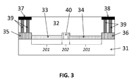
- Figure 2 shows a cross-section along line A-A' (optical modulation section 21) and Figure 3 shows a cross-section along line B-B' (optical power monitoring section 22) of the micro-ring waveguide 20 of Figure 1 .
- the micro-ring waveguide is a rib waveguide, containing slab portions 201 (shallow etched portions) and a strip portion 202 (unetched portion) wherein light may be confined.
- the core of the micro-ring waveguide 20 is stacked between a lower cladding layer 31 and an upper cladding layer 32.
- the lower cladding layer 31 may for example be a silicon oxide layer, such as an oxide layer of a SOI substrate.
- the upper cladding layer 32 may for example be a deposited silicon oxide layer.
- the rib waveguide comprises an integrated PN junction formed by a P-type region 33 at a first lateral side of the strip portion 202 and an N-type region 34 at a second lateral side of the strip portion 202.
- the P-type region 33 and the N-type region 34 form a lateral PN-junction that is located in the strip portion 202 of the micro-ring waveguide 20.
- the P-type region 33 and the N-type region 34 may for example be formed by ion implantation followed by annealing, e.g. Rapid Thermal Annealing, for dopant activation.
- the doping concentration in the P-type region 33 and in the N-type region 34 may for example be in the order of 10 18 cm -3 , the present disclosure not being limited thereto.
- the location of the PN junction in the strip portion 202 may be at substantially the same lateral position along the length of the optical modulation section 21. In other embodiments of the present disclosure, the location of the PN junction in the strip portion 202 may vary along the length of the optical modulation section 21: the PN junction may for example be interdigitated.
- the micro-ring also contains a P-type contact 37 and an N-type contact 38, to enable tuning of the effective refractive index in the optical modulation section 21 by depleting the PN junction (reverse biasing) inside the micro-ring waveguide 20.
- a heavily doped P + region 35 and a heavily doped N + region 36 are formed in the silicon layer at the location of respectively the P-type contact 37 and the N-type contact 38 to enable the formation of good ohmic contacts.
- the P + -type region and the N + -type region may for example be formed by ion implantation followed by annealing, e.g. Rapid Thermal Annealing, for dopant activation.
- the doping concentration in the P + -type region and in the N + -type region may for example be in the order of 10 20 cm -3 , the present disclosure not being limited thereto.
- the P-type contact 37 may for example be electrically connected to the heavily doped P + region 35 though the upper cladding layer 32 by means of electrically conductive plugs 39.
- the N-type contact 38 may for example be electrically connected to the heavily doped N+ region 36 though the upper cladding layer 32 by means of electrically conductive plugs 39.
- the micro-ring waveguide shown is a rib waveguide, wherein an electrical path between the heavily doped P + region 35 (p-type contact 37) and the PN junction in the strip portion 202 of the waveguide and between the heavily doped N + region 36 (N-type contact 38) and the PN junction is established through the doped slab portions 201
- the micro-ring waveguide may be a strip waveguide, wherein an electrical path is established between the contacts and a PN junction in the strip waveguide by forming doped silicon bridges between the contact areas and the strip waveguide.
- Other suitable configurations may be used.
- the rib waveguide comprises a P-type region 33 at a first lateral side of the strip portion 202, an N-type region 34 at a second lateral side of the strip portion, and a doping compensated region 40 between the P-type region 33 and the N-type region 34, the doping compensated region 40 being located in the strip portion 202.
- a lateral PIN diode is formed, with the doping compensated, e.g. intrinsic, region located in the strip portion of the micro-ring.
- the P-type region 33 and the N-type region 34 both extend into the strip portion of the micro-ring, the present disclosure is not limited thereto.
- the doping compensated region 40 is a region with a high defect density. This high defect density may for example be obtained by doping compensation.
- the doping compensated region 40 may for example be formed as a result of the ion implantation steps that are used for forming the P-type region 33 and the N-type region 34 (both in the optical power monitoring section 22 and in the optical modulation section 21), by providing an overlap between both ion implantation windows.
- the doping compensated region 40 may for example be formed as a result of the ion implantation steps that are performed for forming the P + -type region 35 and the N + -type region 36, by providing an overlap between both ion implantation windows.
- an overlap between ion implantation windows may be provided for both the P-type and N-type implantation and the P + -type and N + -type implantation to form the compensated region 40.
- the N-type dopants and the P-type dopants may at least partially, e.g. completely, compensate each other and a doping compensated region 40, such as for example an intrinsic region, may be formed.
- a doping compensated region 40 such as for example an intrinsic region
- the free carrier concentration remains low in the doping compensated region 40, which eliminates undesired free carrier absorption.
- the density of lattice defects doubles in this region 40 due to the repeated ion implantations. The lattice defects result in defect states in the forbidden band of silicon.
- photons at 1.55 ⁇ m whose energy is below the gap of the forbidden band may excite electrons from the valence band to the conduction band, which is well-known as defect mediated sub-bandgap absorption.
- defect mediated sub-bandgap absorption the optical-to-electrical conversion quantum efficiency of the defect mediated absorption is proportional to the defect density.
Landscapes
- Physics & Mathematics (AREA)
- Nonlinear Science (AREA)
- General Physics & Mathematics (AREA)
- Optics & Photonics (AREA)
- Optical Modulation, Optical Deflection, Nonlinear Optics, Optical Demodulation, Optical Logic Elements (AREA)
Abstract
Description
- The present disclosure is related to carrier-depletion based silicon waveguide resonant cavity modulators having an integrated optical power monitor, and to methods for fabricating such resonant cavity modulators with integrated power monitor.
- A carrier-depletion based silicon waveguide resonant cavity modulator of the present disclosure may be integrated on a silicon photonics platform without the need for additional process steps.
- An objective of silicon photonics is to integrate different functionalities, including wavelength multiplexing and de-multiplexing, routing, optical emission, modulation, and detection on a silicon based platform, such as a silicon-on-oxide (SOI) based platform.
- A compact, power-efficient and high-speed integrated silicon modulator is a key building block of silicon photonics. The carrier-depletion modulator is becoming a preferred solution for electro-optic modulation in silicon, because of its compatibility with complementary metal-oxide semiconductor (CMOS) process technology, its processing simplicity, and its high operation speed.
- For example, a carrier-depletion based micro-ring modulator comprises a micro-ring resonator with an integrated PN junction, the micro-ring being coupled to a neighboring waveguide. The resonant wavelength may be modified by tuning the effective refractive index of the micro-ring waveguide. Tuning is obtained by reverse biasing the PN junction integrated with the micro-ring.
- Due to its resonant nature, the micro-ring modulator has the advantages of compact size, low power consumption, and low driving voltage. However, a drawback of this structure is that optical modulation occurs only within a narrow wavelength range near the resonance wavelength. A typical optical bandwidth of effective modulation is less than 0.1 nm.
- Further, a silicon waveguide is very sensitive to temperature variations. A change of the ambient temperature with 1°C results in a shift of the resonance wavelength of a silicon micro-ring modulator by about 0.1 nm. This makes the silicon micro-ring modulator very sensitive to any temperature fluctuation.
- Therefore, a silicon micro-ring modulator needs to be integrated with a dynamic thermal stabilization system. Such dynamic thermal stabilization system may include a heater to change the temperature, a feedback circuit to control the heater power, and an optical power monitor which monitors the ring dynamics and which provides a feedback signal to the circuit controlling the heater power.
- The 1.12 eV band gap of silicon makes it transparent in the telecom wavelength band around 1.55 µm. In order to enable monitoring of the optical power inside a silicon micro-ring modulator, several solutions have been proposed, such as: integration of a Germanium photodetector by eptiaxial growth; bonding of a III-V semiconductor based photodetector; or using a dedicated ion implantation step (typically Si+ implantation) to introduce lattice defects in the silicon waveguide in a predetermined area. These lattice defects may lead to defect-state mediated sub-bandgap absorption, resulting in the generation of a photocurrent. While the observed effect is generally much weaker than in case of direct absorption in a Ge or III-V photo-detector, it is an advantage of this approach that the functionality may be implemented relying exclusively on silicon carrier-depletion modulation without adding processing steps.
- A silicon micro-ring modulator wherein defect-state mediated absorption is used for integrated power monitoring has been described by Hui Yu et al in "Using carrier-depletion silicon modulators for optical power monitoring", Optics Letters Vol.37, No. 22, 2012. A micro-ring resonator with a lateral PN junction is described, wherein the PN junction is embedded in an SOI waveguide by ion implantation. After ion implantation, a rapid thermal annealing (RTA) is done at a temperature above 1000°C to activate the dopants and to repair damage in the silicon lattice without causing much dopant redistribution. Still, there remain some residual crystal defects that can mediate sub-bandgap absorption. It is shown that, after being heated to 1075°C, a reverse-biased PN diode still produces a substantial photocurrent, based on defect-mediated absorption in the ion-implanted SOI waveguides. This photocurrent is used as a power monitor feedback signal. This means that the widely utilized carrier-depletion modulator may also be used for optical power monitoring without any additional processing. For example, a small section of a PN-junction-embedded ring may be used to monitor the optical power inside the ring. It is suggested that the responsivity of both the modulator and the monitor may be enhanced by using an interdigitated PN junction instead of a lateral PN junction, to enlarge the overlap between the optical mode and the carrier-depletion region, or by reducing the RTA temperature to increase the crystal defect density.
- The present disclosure aims to provide a carrier-depletion based silicon waveguide resonant cavity modulator with an integrated optical power monitor based on defect-mediated sub-bandgap absorption, wherein the power monitor has a good responsivity, and wherein the power monitor may be integrated without the need for additional processing steps and without introducing any additional absorption materials. The present disclosure further aims to provide a method for fabricating such resonant cavity modulator with integrated power monitor.
- The present disclosure is related to a carrier-depletion based silicon waveguide resonant cavity modulator comprising a silicon waveguide based resonant cavity, the resonant cavity comprising an optical modulation section and an optical power monitoring section, wherein the optical modulation section comprises an integrated lateral PN diode and wherein the optical power monitoring section comprises an integrated lateral PIN diode comprising a doping compensated I region having a high defect density and a low net free carrier concentration.
- In the context of the present disclosure, the term "PIN diode" refers to a diode having a p-type semiconductor region (P) and an n-type semiconductor region (N) with there in between a semiconductor region (I) having a net doping concentration that is lower than the net P-type doping concentration of the P region and lower than the net N-type doping concentration of the N region. In embodiments of the present disclosure the doping compensated region (I region) may be an intrinsic region or a near intrinsic region, or it may be a lowly doped p-type region or a lowly doped n-type region.
- In operation, when light propagates through the resonant cavity silicon waveguide, free photo-carriers may be generated in the PIN diode through defect mediated absorption, resulting in a photocurrent. The photocurrent is a measure for the optical power inside the resonant cavity and may be used as a feedback signal to a circuit controlling a heater power.
- In a fabrication process of a carrier-depletion based silicon waveguide resonant cavity modulator of the present disclosure, the doping compensated region may for example be formed by performing a P-type implantation step using a first implantation window and by performing an N-type implantation step using a second implantation window, with overlapping first and second ion implantation windows at the location where the doping compensated region is to be provided. The same ion implantation steps as used in the fabrication of the optical modulation section of the carrier-depletion based modulator may be used to realize the in-waveguide optical power monitor. Therefore a PIN photodiode wherein photocarriers are generated through defect mediated absorption may be obtained inside a waveguide based resonant cavity using the same process flow as used for fabricating the carrier-depletion based modulator.
- In embodiments of the present disclosure, the waveguide resonant cavity may for example comprise a micro-ring resonator or a Fabry-Pérot cavity, the present disclosure not being limited thereto.
- It is an advantage of devices and methods of the present disclosure that there is no need for using non-silicon photoactive materials such as Ge or III-V semiconductor materials to enable optical power monitoring.
- It is an advantage of devices and methods of the present disclosure that the doping compensated region may have a high defect density, resulting in a good photocurrent (good responsivity) through defect mediated absorption, while having a low net free carrier concentration, thus avoiding or reducing undesired free carrier absorption losses.
- It is an advantage of devices and methods of the present disclosure that there is no need for additional processing steps to realize the PIN photodiode. The processing of the PIN photodiode is fully compatible with the processing of the silicon carrier-depletion modulator. Therefore the power monitor (PIN diode) may be integrated without additional cost.
- It is an advantage of embodiments of the present disclosure that the optical power monitor may be provided directly inside the waveguide based resonant cavity modulator, thus leading to a reduced complexity of the photonics circuit.
- Certain objects and advantages of various inventive aspects have been described herein above. Of course, it is to be understood that not necessarily all such objects or advantages may be achieved in accordance with any particular embodiment of the disclosure. Thus, for example, those skilled in the art will recognize that the disclosure may be embodied or carried out in a manner that achieves or optimizes one advantage or group of advantages as taught herein without necessarily achieving other objects or advantages as may be taught or suggested herein. Further, it is understood that this summary is merely an example and is not intended to limit the scope of the disclosure. The disclosure, both as to organization and method of operation, together with features and advantages thereof, may best be understood by reference to the following detailed description when read in conjunction with the accompanying drawings.
-
-
Figure 1 schematically illustrates a micro-ring comprising an optical modulation section and an optical power monitoring section in accordance with an embodiment of the present disclosure. -
Figure 2 schematically shows a cross section along line A-A' (Figure 1 ) of the optical modulation section of a micro-ring according to an embodiment of the present disclosure. -
Figure 3 schematically shows a cross section along line B-B' (Figure 1 ) of the optical power monitoring section of a micro-ring according to an embodiment of the present disclosure. - Any reference signs in the claims shall not be construed as limiting the scope of the present disclosure.
- In the different drawings, the same reference signs refer to the same or analogous elements.
- In the following detailed description, numerous specific details are set forth in order to provide a thorough understanding of the disclosure and how it may be practiced in particular embodiments. However, it will be understood that the present disclosure may be practiced without these specific details. In other instances, well-known methods, procedures and techniques have not been described in detail, so as not to obscure the present disclosure.
- The present disclosure will be described with respect to particular embodiments and with reference to certain drawings but the disclosure is not limited thereto but only by the claims. The drawings described are only schematic and are non-limiting. In the drawings, the size of some of the elements may be exaggerated and not drawn on scale for illustrative purposes. The dimensions and the relative dimensions do not necessarily correspond to actual reductions to practice of the disclosure.
- Furthermore, the terms first, second, third and the like in the description and in the claims, are used for distinguishing between similar elements and not necessarily for describing a sequential or chronological order. The terms are interchangeable under appropriate circumstances and the embodiments of the disclosure can operate in other sequences than described or illustrated herein.
- Moreover, the terms top, bottom, over, under and the like in the description and the claims are used for descriptive purposes and not necessarily for describing relative positions. It is to be understood that the terms so used are interchangeable under appropriate circumstances and that the embodiments of the disclosure described herein are capable of operation in other orientations than described or illustrated herein.
- The term "comprising", used in the claims, should not be interpreted as being restricted to the means listed thereafter; it does not exclude other elements or steps. It needs to be interpreted as specifying the presence of the stated features, integers, steps or components as referred to, but does not preclude the presence or addition of one or more other features, integers, steps or components, or groups thereof. Thus, the scope of the expression "a device comprising means A and B" should not be limited to devices consisting only of components A and B.
- The present disclosure relates to a carrier-depletion based silicon waveguide resonant cavity modulator with an integrated optical power monitor based on defect mediated carrier absorption, wherein the power monitor has an improved responsivity as compared to prior art power monitors, and wherein the power monitor may be integrated without the need for additional processing steps and without introducing any additional absorption materials.
- The present disclosure is further described for embodiments wherein the silicon waveguide resonant cavity modulator is a silicon micro-ring modulator. However, the present disclosure is not limited thereto. The silicon waveguide resonant cavity may for example be a Fabry-Pérot cavity or any other suitable cavity known by a person skilled in the art.
-
Figure 1 schematically illustrates a micro-ring modulator according to an embodiment of the present disclosure (top view). The modulator comprises afirst waveguide 10, which may for example be a straight waveguide as shown inFigure 1 , the present disclosure not being limited thereto, and asecond waveguide 20 having a micro-ring shape, thesecond waveguide 20 being optically coupled to thefirst waveguide 10 by evanescent coupling. Themicro-ring waveguide 20 comprises anoptical modulation section 21 and an opticalpower monitoring section 22. - In the example shown in
Figure 1 , thesecond waveguide 20 has a ring shape. However, the present disclosure is not limited thereto and any other suitable (closed) shape known to a person skilled in the art may be used forsecond waveguide 20, such as for example a racetrack shape or a rectangular shape with rounded corners. - In embodiments of the present disclosure, the
first waveguide 10 and the second waveguide 20 (e.g. micro-ring) may for example have a silicon core layer and silicon oxide cladding layers. For example, the waveguide core may be formed in the device layer of an SOI substrate. However, the present disclosure is not limited thereto and other suitable material combinations may be used. - In embodiments of the present disclosure, the micro-ring modulator is a carrier depletion-based modulator with an integrated PN junction.
-
Figure 2 shows a cross-section along line A-A' (optical modulation section 21) andFigure 3 shows a cross-section along line B-B' (optical power monitoring section 22) of themicro-ring waveguide 20 ofFigure 1 . In the example illustrated inFigure 2 andFigure 3 , the micro-ring waveguide is a rib waveguide, containing slab portions 201 (shallow etched portions) and a strip portion 202 (unetched portion) wherein light may be confined. The core of themicro-ring waveguide 20 is stacked between alower cladding layer 31 and anupper cladding layer 32. Thelower cladding layer 31 may for example be a silicon oxide layer, such as an oxide layer of a SOI substrate. Theupper cladding layer 32 may for example be a deposited silicon oxide layer. - In the
optical modulation section 21 of the micro-ring (Figure 2 ), the rib waveguide comprises an integrated PN junction formed by a P-type region 33 at a first lateral side of thestrip portion 202 and an N-type region 34 at a second lateral side of thestrip portion 202. The P-type region 33 and the N-type region 34 form a lateral PN-junction that is located in thestrip portion 202 of themicro-ring waveguide 20. The P-type region 33 and the N-type region 34 may for example be formed by ion implantation followed by annealing, e.g. Rapid Thermal Annealing, for dopant activation. The doping concentration in the P-type region 33 and in the N-type region 34 may for example be in the order of 1018 cm-3, the present disclosure not being limited thereto. - In embodiments of the present disclosure, the location of the PN junction in the
strip portion 202 may be at substantially the same lateral position along the length of theoptical modulation section 21. In other embodiments of the present disclosure, the location of the PN junction in thestrip portion 202 may vary along the length of the optical modulation section 21: the PN junction may for example be interdigitated. - As illustrated in
Figure 2 , the micro-ring also contains a P-type contact 37 and an N-type contact 38, to enable tuning of the effective refractive index in theoptical modulation section 21 by depleting the PN junction (reverse biasing) inside themicro-ring waveguide 20. A heavily doped P+ region 35 and a heavily doped N+ region 36 are formed in the silicon layer at the location of respectively the P-type contact 37 and the N-type contact 38 to enable the formation of good ohmic contacts. The P+-type region and the N+-type region may for example be formed by ion implantation followed by annealing, e.g. Rapid Thermal Annealing, for dopant activation. The doping concentration in the P+-type region and in the N+-type region may for example be in the order of 1020cm-3, the present disclosure not being limited thereto. The P-type contact 37 may for example be electrically connected to the heavily doped P+ region 35 though theupper cladding layer 32 by means of electrically conductive plugs 39. Similarly, the N-type contact 38 may for example be electrically connected to the heavily dopedN+ region 36 though theupper cladding layer 32 by means of electrically conductive plugs 39. - Although in
Figure 2 the micro-ring waveguide shown is a rib waveguide, wherein an electrical path between the heavily doped P+ region 35 (p-type contact 37) and the PN junction in thestrip portion 202 of the waveguide and between the heavily doped N+ region 36 (N-type contact 38) and the PN junction is established through the dopedslab portions 201, the present disclosure is not limited thereto. For example, the micro-ring waveguide may be a strip waveguide, wherein an electrical path is established between the contacts and a PN junction in the strip waveguide by forming doped silicon bridges between the contact areas and the strip waveguide. Other suitable configurations may be used. - In the optical
power monitoring section 22, schematically illustrated inFigure 3 , the rib waveguide comprises a P-type region 33 at a first lateral side of thestrip portion 202, an N-type region 34 at a second lateral side of the strip portion, and a doping compensatedregion 40 between the P-type region 33 and the N-type region 34, the doping compensatedregion 40 being located in thestrip portion 202. In this way a lateral PIN diode is formed, with the doping compensated, e.g. intrinsic, region located in the strip portion of the micro-ring. Although in the example illustrated inFigure 3 , the P-type region 33 and the N-type region 34 both extend into the strip portion of the micro-ring, the present disclosure is not limited thereto. - In embodiments of the present disclosure, the doping compensated
region 40 is a region with a high defect density. This high defect density may for example be obtained by doping compensation. In embodiments of the present disclosure, the doping compensatedregion 40 may for example be formed as a result of the ion implantation steps that are used for forming the P-type region 33 and the N-type region 34 (both in the opticalpower monitoring section 22 and in the optical modulation section 21), by providing an overlap between both ion implantation windows. In other embodiments, the doping compensatedregion 40 may for example be formed as a result of the ion implantation steps that are performed for forming the P+-type region 35 and the N+-type region 36, by providing an overlap between both ion implantation windows. In still other embodiments an overlap between ion implantation windows may be provided for both the P-type and N-type implantation and the P+-type and N+-type implantation to form the compensatedregion 40. - By providing an overlap between the P-type (P+-type) ion implantation window and the N-type (N+-type) ion implantation window in the optical
power monitoring section 22, in thestrip portion 202 of the waveguide, the N-type dopants and the P-type dopants may at least partially, e.g. completely, compensate each other and a doping compensatedregion 40, such as for example an intrinsic region, may be formed. As a result, the free carrier concentration remains low in the doping compensatedregion 40, which eliminates undesired free carrier absorption. On the other hand, the density of lattice defects doubles in thisregion 40 due to the repeated ion implantations. The lattice defects result in defect states in the forbidden band of silicon. Through these states, photons at 1.55 µm whose energy is below the gap of the forbidden band may excite electrons from the valence band to the conduction band, which is well-known as defect mediated sub-bandgap absorption. Generally the optical-to-electrical conversion quantum efficiency of the defect mediated absorption is proportional to the defect density. - It is an advantage of embodimens of the present disclosure that only existing ion implantation steps which are indispensable to implement a carrier-depletion based modulator may be used, so no additional processing steps are required.
- In operation, when light propagates through the micro-ring 20, part of the propagating light is absorbed by defect mediated absorption in the
power monitoring section 22 of the micro-ring. This absorption gives rise to a photocurrent that is a measure for the optical power inside the micro-ring. This photocurrent may be used as a feedback signal towards a feedback control circuit that adjusts the power of an integrated heater, so as to dynamically control the operation wavelength of the ring modulator. - The foregoing description details certain embodiments of the disclosure. It will be appreciated, however, that no matter how detailed the foregoing appears in text, the disclosure may be practiced in many ways. It should be noted that the use of particular terminology when describing certain features or aspects of the disclosure should not be taken to imply that the terminology is being re-defined herein to be restricted to including any specific characteristics of the features or aspects of the disclosure with which that terminology is associated.
- While the above detailed description has shown, described, and pointed out novel features of the invention as applied to various embodiments, it will be understood that various omissions, substitutions, and changes in the form and details of the device or process illustrated may be made by those skilled in the technology without departing from the invention.
Claims (7)
- A carrier-depletion based silicon waveguide resonant cavity modulator comprising a silicon waveguide based resonant cavity (20), the resonant cavity comprising an optical modulation section (21) and an optical power monitoring section (22), characterized in that the optical power monitoring section (22) comprises an integrated lateral PIN diode comprising a doping compensated I region having a high defect density.
- The carrier-depletion based silicon waveguide resonant cavity modulator according to claim 1, wherein the lateral PIN diode comprises a P-doped region having a net P-type doping concentration, an N-doped region having a net N-type doping concentration and a doping compensated I-region, the I-region having a net doping concentration that is lower than the net P-type doping concentration and lower than the net N-type concentration.
- The carrier-depletion based silicon waveguide resonant cavity modulator according to claim 1 or claim 2 wherein the doping compensated region is an intrinsic region.
- The carrier-depletion based silicon waveguide resonant cavity modulator according to any of claims 1 to 3 wherein the resonant cavity comprises a micro-ring resonator.
- The carrier-depletion based silicon waveguide resonant cavity modulator according to any of claims 1 to 3 wherein the resonant cavity comprises a Fabry-Pérot cavity.
- A method for fabricating a carrier-depletion based silicon waveguide resonant cavity modulator comprising a silicon waveguide based resonant cavity (20), the resonant cavity comprising an optical modulation section (21) with an integrated lateral PN diode and an optical power monitoring section (22) with an integrated lateral PIN diode comprising a doping compensated I region, wherein the method comprises:performing a P-type implantation step using a first implantation window; andperforming an N-type implantation step using a second implantation window,wherein an overlap is provided between the first implantation window and the second implantation window, thereby forming the doping compensated region at the locations of the overlap.
- The method according to claim 6 wherein performing the P-type implantation step comprises forming a P-type region of the PN diode and the PIN diode and wherein performing the N-type implantation comprises forming the N-type region of the PN diode and the PIN diode.
Priority Applications (1)
| Application Number | Priority Date | Filing Date | Title |
|---|---|---|---|
| EP14172997.0A EP2829906B1 (en) | 2013-07-23 | 2014-06-18 | Carrier-depletion based silicon waveguide resonant cavity modulator with integrated optical power monitor |
Applications Claiming Priority (2)
| Application Number | Priority Date | Filing Date | Title |
|---|---|---|---|
| EP13177675 | 2013-07-23 | ||
| EP14172997.0A EP2829906B1 (en) | 2013-07-23 | 2014-06-18 | Carrier-depletion based silicon waveguide resonant cavity modulator with integrated optical power monitor |
Publications (2)
| Publication Number | Publication Date |
|---|---|
| EP2829906A1 true EP2829906A1 (en) | 2015-01-28 |
| EP2829906B1 EP2829906B1 (en) | 2018-11-28 |
Family
ID=48856529
Family Applications (1)
| Application Number | Title | Priority Date | Filing Date |
|---|---|---|---|
| EP14172997.0A Active EP2829906B1 (en) | 2013-07-23 | 2014-06-18 | Carrier-depletion based silicon waveguide resonant cavity modulator with integrated optical power monitor |
Country Status (2)
| Country | Link |
|---|---|
| US (1) | US9678370B2 (en) |
| EP (1) | EP2829906B1 (en) |
Cited By (2)
| Publication number | Priority date | Publication date | Assignee | Title |
|---|---|---|---|---|
| JP2017045012A (en) * | 2015-08-28 | 2017-03-02 | 日本電信電話株式会社 | Light modulator |
| WO2021105138A1 (en) * | 2019-11-26 | 2021-06-03 | Rockley Photonics Limited | Integrated iii-v / silicon optoelectronic device and method of manufacture thereof |
Families Citing this family (14)
| Publication number | Priority date | Publication date | Assignee | Title |
|---|---|---|---|---|
| WO2014185951A1 (en) * | 2013-05-14 | 2014-11-20 | Silicon Lightwave Services | Ultra-responsive phase shifters for depletion mode silicon modulators |
| US10027420B2 (en) * | 2014-06-26 | 2018-07-17 | Luxtera, Inc. | Method and system for a silicon-based optical phase modulator with high modal overlap |
| EP3518280B1 (en) * | 2018-01-25 | 2020-11-04 | Murata Manufacturing Co., Ltd. | Electronic product having embedded porous dielectric and method of manufacture |
| CN110109266A (en) * | 2018-02-01 | 2019-08-09 | 上海硅通半导体技术有限公司 | A kind of silicon substrate absorption-type electrooptic modulator and the method for improving modulation efficiency |
| US10241354B1 (en) | 2018-03-14 | 2019-03-26 | International Business Machines Corporation | Electro-optic modulator with a periodic junction arrangement |
| US10215925B1 (en) * | 2018-08-22 | 2019-02-26 | Mcmaster University | Systems and methods for resonance stabilization of microring resonator |
| FR3090909B1 (en) * | 2018-12-20 | 2021-05-07 | St Microelectronics Crolles 2 Sas | Ring resonator electro-optic device |
| US11262637B2 (en) * | 2019-01-14 | 2022-03-01 | Luxtera Llc | Method and system for a frequency diverse distributed Mach-Zehnder Interferometer |
| US11874538B2 (en) * | 2020-09-30 | 2024-01-16 | Taiwan Semiconductor Manufacturing Company Limited | Apparatus and method for generating an optical signal |
| CN113933931B (en) * | 2021-08-27 | 2024-06-21 | 北京工业大学 | A ring cavity optical modulator based on vanadium dioxide nanowires |
| US11726264B2 (en) * | 2022-01-18 | 2023-08-15 | Hewlett Packard Enterprise Development Lp | Optical device having waveguide integrated modulator and light monitoring avalanche photodiode |
| CN114894301B (en) * | 2022-04-11 | 2025-07-22 | 南京大学 | Terahertz detector integrated with whispering gallery mode waveguide on chip |
| CN115598871B (en) * | 2022-10-12 | 2025-10-24 | 上海交通大学 | Silicon-based electro-optical modulator based on micro-ring structure and modulation method thereof |
| WO2025151570A1 (en) * | 2024-01-09 | 2025-07-17 | Ayar Labs, Inc. | Low non-linear loss silicon waveguides for evanescent couplers |
Citations (2)
| Publication number | Priority date | Publication date | Assignee | Title |
|---|---|---|---|---|
| GB2383684A (en) * | 2001-12-27 | 2003-07-02 | Bookham Technology Plc | A light sensor |
| US20110091146A1 (en) * | 2009-07-20 | 2011-04-21 | Knights Andrew P | Optical modulators employing charge state control of deep levels |
Family Cites Families (4)
| Publication number | Priority date | Publication date | Assignee | Title |
|---|---|---|---|---|
| US6879014B2 (en) * | 2000-03-20 | 2005-04-12 | Aegis Semiconductor, Inc. | Semitransparent optical detector including a polycrystalline layer and method of making |
| EP1415191A1 (en) * | 2001-08-02 | 2004-05-06 | Aegis Semiconductor | Tunable optical instruments |
| US8883589B2 (en) * | 2010-09-28 | 2014-11-11 | Sandisk 3D Llc | Counter doping compensation methods to improve diode performance |
| US9134169B2 (en) * | 2012-10-19 | 2015-09-15 | The Hong Kong University Of Science And Technology | In-microresonator linear-absorption-based real-time photocurrent-monitoring and tuning with closed-loop control for silicon microresonators |
-
2014
- 2014-06-18 EP EP14172997.0A patent/EP2829906B1/en active Active
- 2014-07-23 US US14/338,564 patent/US9678370B2/en active Active
Patent Citations (2)
| Publication number | Priority date | Publication date | Assignee | Title |
|---|---|---|---|---|
| GB2383684A (en) * | 2001-12-27 | 2003-07-02 | Bookham Technology Plc | A light sensor |
| US20110091146A1 (en) * | 2009-07-20 | 2011-04-21 | Knights Andrew P | Optical modulators employing charge state control of deep levels |
Non-Patent Citations (7)
| Title |
|---|
| DYLAN F LOGAN ET AL: "Monitoring and Tuning Micro-Ring Properties Using Defect-Enhanced Silicon Photodiodes at 1550 nm", IEEE PHOTONICS TECHNOLOGY LETTERS, IEEE SERVICE CENTER, PISCATAWAY, NJ, US, vol. 24, no. 4, 1 February 2012 (2012-02-01), pages 261 - 263, XP011398615, ISSN: 1041-1135, DOI: 10.1109/LPT.2011.2177453 * |
| ELLIOTT C T ET AL: "Counterdoped extrinsic silicon infrared detectors", INFRARED PHYSICS, PERGAMON, vol. 18, no. 2, 1 March 1978 (1978-03-01), pages 65 - 71, XP024583546, ISSN: 0020-0891, [retrieved on 19780301], DOI: 10.1016/0020-0891(78)90014-3 * |
| HUI YU ET AL.: "Using carrier-depletion silicon modulators for optical power monitoring", OPTICS LETTERS, vol. 37, no. 22, 2012, XP001579180, DOI: doi:10.1364/OL.37.004681 |
| HUI YU ET AL: "Using carrier-depletion silicon modulators for optical power monitoring", OPTICS LETTERS, vol. 37, no. 22, 15 November 2012 (2012-11-15), pages 4681, XP055132145, ISSN: 0146-9592, DOI: 10.1364/OL.37.004681 * |
| J K DOYLEND ET AL: "Silicon photonic resonator-enhanced defect- mediated photodiode for sub-bandgap detection", OPT. EXPRESS, 5 July 2010 (2010-07-05), pages 14671 - 14678, XP055149036, Retrieved from the Internet <URL:http://www.opticsinfobase.org/DirectPDFAccess/2BA3E467-FCC5-8C3E-31ED1FECD8394EB7_202805/oe-18-14-14671.pdf?da=1&id=202805&seq=0&mobile=no> [retrieved on 20141027] * |
| KYLE PRESTON ET AL: "Waveguide-integrated telecom-wavelength photodiode in deposited silicon", OPTICS LETTERS, OPTICAL SOCIETY OF AMERICA, US, vol. 36, no. 1, 1 January 2011 (2011-01-01), pages 52 - 54, XP001559805, ISSN: 0146-9592, DOI: 10.1364/OL.36.000052 * |
| MAURIZIO CASALINO ET AL: "Near-Infrared Sub-Bandgap All-Silicon Photodetectors: State of the Art and Perspectives", SENSORS, vol. 10, no. 12, 29 December 2010 (2010-12-29), pages 10571 - 10600, XP055139465, ISSN: 1424-8220, DOI: 10.3390/s101210571 * |
Cited By (3)
| Publication number | Priority date | Publication date | Assignee | Title |
|---|---|---|---|---|
| JP2017045012A (en) * | 2015-08-28 | 2017-03-02 | 日本電信電話株式会社 | Light modulator |
| WO2021105138A1 (en) * | 2019-11-26 | 2021-06-03 | Rockley Photonics Limited | Integrated iii-v / silicon optoelectronic device and method of manufacture thereof |
| US12197050B2 (en) | 2019-11-26 | 2025-01-14 | Rockley Photonics Limited | Integrated III-V / silicon optoelectronic device and method of manufacture thereof |
Also Published As
| Publication number | Publication date |
|---|---|
| US20150316795A1 (en) | 2015-11-05 |
| US9678370B2 (en) | 2017-06-13 |
| EP2829906B1 (en) | 2018-11-28 |
Similar Documents
| Publication | Publication Date | Title |
|---|---|---|
| EP2829906B1 (en) | Carrier-depletion based silicon waveguide resonant cavity modulator with integrated optical power monitor | |
| US9343638B2 (en) | Electro-optic PN junction modulator formed with a self-aligned process | |
| EP3349252B1 (en) | Optical waveguide detector and optical module | |
| US10025159B2 (en) | Output monitoring method for optical modulator and output monitoring device | |
| Fang et al. | Recent progress in silicon photonics: a review | |
| US9134169B2 (en) | In-microresonator linear-absorption-based real-time photocurrent-monitoring and tuning with closed-loop control for silicon microresonators | |
| EP3038167B1 (en) | Integrated avalanche germanium photodetector | |
| JP2008526003A (en) | Germanium-on-silicon photodetector | |
| Li et al. | 40 Gb/s all-silicon photodetector based on microring resonators | |
| JP2012053399A (en) | Optical modulation element | |
| CN108054632A (en) | Carrier depletion type micro-ring resonator wavelength locking method with multiplexing functions | |
| CN103137777A (en) | Semiconductor optical device | |
| JPWO2016157687A1 (en) | Electro-optic device | |
| US20210173237A1 (en) | Polarization splitter-rotator with embedded pin structure | |
| CN105388638A (en) | Silicon waveguide thermo-optic adjusting structure | |
| Spector et al. | Operation and optimization of silicon-diode-based optical modulators | |
| Zhao et al. | Efficient mid-infrared germanium variable optical attenuator fabricated by spin-on-glass doping | |
| Samusenko et al. | Integrated silicon photodetector for lab-on-chip sensor platform | |
| Li et al. | Optical power monitoring with ultrahigh sensitivity in silicon waveguides and ring resonators | |
| CN100407378C (en) | Polycrystalline germanium-based waveguide detector integrated on epitaxial silicon thin plate on insulating substrate | |
| Van Engelen et al. | A novel optically wide-band electro-absorption modulator based on bandfilling in n-InGaAs | |
| Park et al. | Monolithic integration of InGaAsP MZI modulator and InGaAs driver MOSFET using III-V CMOS photonics | |
| Benedikovic et al. | High-performance waveguide photodetectors based on lateral Si/Ge/Si heterojunction | |
| US9684194B2 (en) | Method for making electro-optical device | |
| Lim et al. | Germanium electro-absorption modulator for power efficient optical links |
Legal Events
| Date | Code | Title | Description |
|---|---|---|---|
| 17P | Request for examination filed |
Effective date: 20140618 |
|
| AK | Designated contracting states |
Kind code of ref document: A1 Designated state(s): AL AT BE BG CH CY CZ DE DK EE ES FI FR GB GR HR HU IE IS IT LI LT LU LV MC MK MT NL NO PL PT RO RS SE SI SK SM TR |
|
| AX | Request for extension of the european patent |
Extension state: BA ME |
|
| PUAI | Public reference made under article 153(3) epc to a published international application that has entered the european phase |
Free format text: ORIGINAL CODE: 0009012 |
|
| R17P | Request for examination filed (corrected) |
Effective date: 20150702 |
|
| RBV | Designated contracting states (corrected) |
Designated state(s): AL AT BE BG CH CY CZ DE DK EE ES FI FR GB GR HR HU IE IS IT LI LT LU LV MC MK MT NL NO PL PT RO RS SE SI SK SM TR |
|
| GRAP | Despatch of communication of intention to grant a patent |
Free format text: ORIGINAL CODE: EPIDOSNIGR1 |
|
| STAA | Information on the status of an ep patent application or granted ep patent |
Free format text: STATUS: GRANT OF PATENT IS INTENDED |
|
| INTG | Intention to grant announced |
Effective date: 20180618 |
|
| GRAS | Grant fee paid |
Free format text: ORIGINAL CODE: EPIDOSNIGR3 |
|
| GRAA | (expected) grant |
Free format text: ORIGINAL CODE: 0009210 |
|
| STAA | Information on the status of an ep patent application or granted ep patent |
Free format text: STATUS: THE PATENT HAS BEEN GRANTED |
|
| AK | Designated contracting states |
Kind code of ref document: B1 Designated state(s): AL AT BE BG CH CY CZ DE DK EE ES FI FR GB GR HR HU IE IS IT LI LT LU LV MC MK MT NL NO PL PT RO RS SE SI SK SM TR |
|
| REG | Reference to a national code |
Ref country code: CH Ref legal event code: EP |
|
| REG | Reference to a national code |
Ref country code: AT Ref legal event code: REF Ref document number: 1070915 Country of ref document: AT Kind code of ref document: T Effective date: 20181215 |
|
| REG | Reference to a national code |
Ref country code: DE Ref legal event code: R096 Ref document number: 602014036813 Country of ref document: DE |
|
| REG | Reference to a national code |
Ref country code: IE Ref legal event code: FG4D |
|
| REG | Reference to a national code |
Ref country code: NL Ref legal event code: MP Effective date: 20181128 |
|
| REG | Reference to a national code |
Ref country code: LT Ref legal event code: MG4D |
|
| REG | Reference to a national code |
Ref country code: AT Ref legal event code: MK05 Ref document number: 1070915 Country of ref document: AT Kind code of ref document: T Effective date: 20181128 |
|
| PG25 | Lapsed in a contracting state [announced via postgrant information from national office to epo] |
Ref country code: BG Free format text: LAPSE BECAUSE OF FAILURE TO SUBMIT A TRANSLATION OF THE DESCRIPTION OR TO PAY THE FEE WITHIN THE PRESCRIBED TIME-LIMIT Effective date: 20190228 Ref country code: IS Free format text: LAPSE BECAUSE OF FAILURE TO SUBMIT A TRANSLATION OF THE DESCRIPTION OR TO PAY THE FEE WITHIN THE PRESCRIBED TIME-LIMIT Effective date: 20190328 Ref country code: NO Free format text: LAPSE BECAUSE OF FAILURE TO SUBMIT A TRANSLATION OF THE DESCRIPTION OR TO PAY THE FEE WITHIN THE PRESCRIBED TIME-LIMIT Effective date: 20190228 Ref country code: HR Free format text: LAPSE BECAUSE OF FAILURE TO SUBMIT A TRANSLATION OF THE DESCRIPTION OR TO PAY THE FEE WITHIN THE PRESCRIBED TIME-LIMIT Effective date: 20181128 Ref country code: ES Free format text: LAPSE BECAUSE OF FAILURE TO SUBMIT A TRANSLATION OF THE DESCRIPTION OR TO PAY THE FEE WITHIN THE PRESCRIBED TIME-LIMIT Effective date: 20181128 Ref country code: LT Free format text: LAPSE BECAUSE OF FAILURE TO SUBMIT A TRANSLATION OF THE DESCRIPTION OR TO PAY THE FEE WITHIN THE PRESCRIBED TIME-LIMIT Effective date: 20181128 Ref country code: LV Free format text: LAPSE BECAUSE OF FAILURE TO SUBMIT A TRANSLATION OF THE DESCRIPTION OR TO PAY THE FEE WITHIN THE PRESCRIBED TIME-LIMIT Effective date: 20181128 Ref country code: AT Free format text: LAPSE BECAUSE OF FAILURE TO SUBMIT A TRANSLATION OF THE DESCRIPTION OR TO PAY THE FEE WITHIN THE PRESCRIBED TIME-LIMIT Effective date: 20181128 Ref country code: FI Free format text: LAPSE BECAUSE OF FAILURE TO SUBMIT A TRANSLATION OF THE DESCRIPTION OR TO PAY THE FEE WITHIN THE PRESCRIBED TIME-LIMIT Effective date: 20181128 |
|
| PG25 | Lapsed in a contracting state [announced via postgrant information from national office to epo] |
Ref country code: GR Free format text: LAPSE BECAUSE OF FAILURE TO SUBMIT A TRANSLATION OF THE DESCRIPTION OR TO PAY THE FEE WITHIN THE PRESCRIBED TIME-LIMIT Effective date: 20190301 Ref country code: AL Free format text: LAPSE BECAUSE OF FAILURE TO SUBMIT A TRANSLATION OF THE DESCRIPTION OR TO PAY THE FEE WITHIN THE PRESCRIBED TIME-LIMIT Effective date: 20181128 Ref country code: RS Free format text: LAPSE BECAUSE OF FAILURE TO SUBMIT A TRANSLATION OF THE DESCRIPTION OR TO PAY THE FEE WITHIN THE PRESCRIBED TIME-LIMIT Effective date: 20181128 Ref country code: SE Free format text: LAPSE BECAUSE OF FAILURE TO SUBMIT A TRANSLATION OF THE DESCRIPTION OR TO PAY THE FEE WITHIN THE PRESCRIBED TIME-LIMIT Effective date: 20181128 Ref country code: PT Free format text: LAPSE BECAUSE OF FAILURE TO SUBMIT A TRANSLATION OF THE DESCRIPTION OR TO PAY THE FEE WITHIN THE PRESCRIBED TIME-LIMIT Effective date: 20190328 |
|
| PG25 | Lapsed in a contracting state [announced via postgrant information from national office to epo] |
Ref country code: NL Free format text: LAPSE BECAUSE OF FAILURE TO SUBMIT A TRANSLATION OF THE DESCRIPTION OR TO PAY THE FEE WITHIN THE PRESCRIBED TIME-LIMIT Effective date: 20181128 |
|
| PG25 | Lapsed in a contracting state [announced via postgrant information from national office to epo] |
Ref country code: IT Free format text: LAPSE BECAUSE OF FAILURE TO SUBMIT A TRANSLATION OF THE DESCRIPTION OR TO PAY THE FEE WITHIN THE PRESCRIBED TIME-LIMIT Effective date: 20181128 Ref country code: DK Free format text: LAPSE BECAUSE OF FAILURE TO SUBMIT A TRANSLATION OF THE DESCRIPTION OR TO PAY THE FEE WITHIN THE PRESCRIBED TIME-LIMIT Effective date: 20181128 Ref country code: CZ Free format text: LAPSE BECAUSE OF FAILURE TO SUBMIT A TRANSLATION OF THE DESCRIPTION OR TO PAY THE FEE WITHIN THE PRESCRIBED TIME-LIMIT Effective date: 20181128 Ref country code: PL Free format text: LAPSE BECAUSE OF FAILURE TO SUBMIT A TRANSLATION OF THE DESCRIPTION OR TO PAY THE FEE WITHIN THE PRESCRIBED TIME-LIMIT Effective date: 20181128 |
|
| REG | Reference to a national code |
Ref country code: DE Ref legal event code: R097 Ref document number: 602014036813 Country of ref document: DE |
|
| PG25 | Lapsed in a contracting state [announced via postgrant information from national office to epo] |
Ref country code: SK Free format text: LAPSE BECAUSE OF FAILURE TO SUBMIT A TRANSLATION OF THE DESCRIPTION OR TO PAY THE FEE WITHIN THE PRESCRIBED TIME-LIMIT Effective date: 20181128 Ref country code: RO Free format text: LAPSE BECAUSE OF FAILURE TO SUBMIT A TRANSLATION OF THE DESCRIPTION OR TO PAY THE FEE WITHIN THE PRESCRIBED TIME-LIMIT Effective date: 20181128 Ref country code: EE Free format text: LAPSE BECAUSE OF FAILURE TO SUBMIT A TRANSLATION OF THE DESCRIPTION OR TO PAY THE FEE WITHIN THE PRESCRIBED TIME-LIMIT Effective date: 20181128 Ref country code: SM Free format text: LAPSE BECAUSE OF FAILURE TO SUBMIT A TRANSLATION OF THE DESCRIPTION OR TO PAY THE FEE WITHIN THE PRESCRIBED TIME-LIMIT Effective date: 20181128 |
|
| PLBE | No opposition filed within time limit |
Free format text: ORIGINAL CODE: 0009261 |
|
| STAA | Information on the status of an ep patent application or granted ep patent |
Free format text: STATUS: NO OPPOSITION FILED WITHIN TIME LIMIT |
|
| PG25 | Lapsed in a contracting state [announced via postgrant information from national office to epo] |
Ref country code: SI Free format text: LAPSE BECAUSE OF FAILURE TO SUBMIT A TRANSLATION OF THE DESCRIPTION OR TO PAY THE FEE WITHIN THE PRESCRIBED TIME-LIMIT Effective date: 20181128 |
|
| 26N | No opposition filed |
Effective date: 20190829 |
|
| PG25 | Lapsed in a contracting state [announced via postgrant information from national office to epo] |
Ref country code: MC Free format text: LAPSE BECAUSE OF FAILURE TO SUBMIT A TRANSLATION OF THE DESCRIPTION OR TO PAY THE FEE WITHIN THE PRESCRIBED TIME-LIMIT Effective date: 20181128 |
|
| REG | Reference to a national code |
Ref country code: CH Ref legal event code: PL |
|
| GBPC | Gb: european patent ceased through non-payment of renewal fee |
Effective date: 20190618 |
|
| REG | Reference to a national code |
Ref country code: BE Ref legal event code: MM Effective date: 20190630 |
|
| PG25 | Lapsed in a contracting state [announced via postgrant information from national office to epo] |
Ref country code: TR Free format text: LAPSE BECAUSE OF FAILURE TO SUBMIT A TRANSLATION OF THE DESCRIPTION OR TO PAY THE FEE WITHIN THE PRESCRIBED TIME-LIMIT Effective date: 20181128 |
|
| PG25 | Lapsed in a contracting state [announced via postgrant information from national office to epo] |
Ref country code: GB Free format text: LAPSE BECAUSE OF NON-PAYMENT OF DUE FEES Effective date: 20190618 Ref country code: IE Free format text: LAPSE BECAUSE OF NON-PAYMENT OF DUE FEES Effective date: 20190618 |
|
| PG25 | Lapsed in a contracting state [announced via postgrant information from national office to epo] |
Ref country code: LI Free format text: LAPSE BECAUSE OF NON-PAYMENT OF DUE FEES Effective date: 20190630 Ref country code: CH Free format text: LAPSE BECAUSE OF NON-PAYMENT OF DUE FEES Effective date: 20190630 Ref country code: BE Free format text: LAPSE BECAUSE OF NON-PAYMENT OF DUE FEES Effective date: 20190630 Ref country code: LU Free format text: LAPSE BECAUSE OF NON-PAYMENT OF DUE FEES Effective date: 20190618 |
|
| PG25 | Lapsed in a contracting state [announced via postgrant information from national office to epo] |
Ref country code: CY Free format text: LAPSE BECAUSE OF FAILURE TO SUBMIT A TRANSLATION OF THE DESCRIPTION OR TO PAY THE FEE WITHIN THE PRESCRIBED TIME-LIMIT Effective date: 20181128 |
|
| PG25 | Lapsed in a contracting state [announced via postgrant information from national office to epo] |
Ref country code: MT Free format text: LAPSE BECAUSE OF FAILURE TO SUBMIT A TRANSLATION OF THE DESCRIPTION OR TO PAY THE FEE WITHIN THE PRESCRIBED TIME-LIMIT Effective date: 20181128 Ref country code: HU Free format text: LAPSE BECAUSE OF FAILURE TO SUBMIT A TRANSLATION OF THE DESCRIPTION OR TO PAY THE FEE WITHIN THE PRESCRIBED TIME-LIMIT; INVALID AB INITIO Effective date: 20140618 |
|
| PG25 | Lapsed in a contracting state [announced via postgrant information from national office to epo] |
Ref country code: MK Free format text: LAPSE BECAUSE OF FAILURE TO SUBMIT A TRANSLATION OF THE DESCRIPTION OR TO PAY THE FEE WITHIN THE PRESCRIBED TIME-LIMIT Effective date: 20181128 |
|
| P01 | Opt-out of the competence of the unified patent court (upc) registered |
Effective date: 20230513 |
|
| PGFP | Annual fee paid to national office [announced via postgrant information from national office to epo] |
Ref country code: DE Payment date: 20250520 Year of fee payment: 12 |
|
| PGFP | Annual fee paid to national office [announced via postgrant information from national office to epo] |
Ref country code: FR Payment date: 20250520 Year of fee payment: 12 |