EP2828086B1 - Druckköpfe mit leiterspuren durch schlitze - Google Patents
Druckköpfe mit leiterspuren durch schlitze Download PDFInfo
- Publication number
- EP2828086B1 EP2828086B1 EP12877853.7A EP12877853A EP2828086B1 EP 2828086 B1 EP2828086 B1 EP 2828086B1 EP 12877853 A EP12877853 A EP 12877853A EP 2828086 B1 EP2828086 B1 EP 2828086B1
- Authority
- EP
- European Patent Office
- Prior art keywords
- slot
- thinfilm
- conductor traces
- examples
- conductor
- Prior art date
- Legal status (The legal status is an assumption and is not a legal conclusion. Google has not performed a legal analysis and makes no representation as to the accuracy of the status listed.)
- Active
Links
- 239000004020 conductor Substances 0.000 title claims description 67
- 239000012530 fluid Substances 0.000 claims description 53
- 239000010409 thin film Substances 0.000 claims description 41
- 239000000758 substrate Substances 0.000 claims description 39
- 239000010410 layer Substances 0.000 claims description 36
- 238000000034 method Methods 0.000 claims description 29
- 238000000151 deposition Methods 0.000 claims description 9
- 238000000059 patterning Methods 0.000 claims description 9
- 230000008569 process Effects 0.000 claims description 8
- 230000008859 change Effects 0.000 claims description 5
- 229910052751 metal Inorganic materials 0.000 claims description 3
- 239000002184 metal Substances 0.000 claims description 3
- 239000011241 protective layer Substances 0.000 claims description 3
- 150000002739 metals Chemical class 0.000 claims description 2
- 238000007639 printing Methods 0.000 description 27
- 239000000463 material Substances 0.000 description 18
- 239000000976 ink Substances 0.000 description 15
- 230000015572 biosynthetic process Effects 0.000 description 10
- 238000005530 etching Methods 0.000 description 7
- 230000005540 biological transmission Effects 0.000 description 4
- WGTYBPLFGIVFAS-UHFFFAOYSA-M tetramethylammonium hydroxide Chemical compound [OH-].C[N+](C)(C)C WGTYBPLFGIVFAS-UHFFFAOYSA-M 0.000 description 4
- RYGMFSIKBFXOCR-UHFFFAOYSA-N Copper Chemical compound [Cu] RYGMFSIKBFXOCR-UHFFFAOYSA-N 0.000 description 3
- VYPSYNLAJGMNEJ-UHFFFAOYSA-N Silicium dioxide Chemical compound O=[Si]=O VYPSYNLAJGMNEJ-UHFFFAOYSA-N 0.000 description 3
- 229910052802 copper Inorganic materials 0.000 description 3
- 239000010949 copper Substances 0.000 description 3
- VYZAMTAEIAYCRO-UHFFFAOYSA-N Chromium Chemical compound [Cr] VYZAMTAEIAYCRO-UHFFFAOYSA-N 0.000 description 2
- 239000004593 Epoxy Substances 0.000 description 2
- PXHVJJICTQNCMI-UHFFFAOYSA-N Nickel Chemical compound [Ni] PXHVJJICTQNCMI-UHFFFAOYSA-N 0.000 description 2
- RTAQQCXQSZGOHL-UHFFFAOYSA-N Titanium Chemical compound [Ti] RTAQQCXQSZGOHL-UHFFFAOYSA-N 0.000 description 2
- 229910052782 aluminium Inorganic materials 0.000 description 2
- XAGFODPZIPBFFR-UHFFFAOYSA-N aluminium Chemical compound [Al] XAGFODPZIPBFFR-UHFFFAOYSA-N 0.000 description 2
- 238000005229 chemical vapour deposition Methods 0.000 description 2
- 239000003086 colorant Substances 0.000 description 2
- 238000005553 drilling Methods 0.000 description 2
- 230000005611 electricity Effects 0.000 description 2
- 230000000977 initiatory effect Effects 0.000 description 2
- 229920000642 polymer Polymers 0.000 description 2
- 230000001737 promoting effect Effects 0.000 description 2
- 239000004065 semiconductor Substances 0.000 description 2
- HBMJWWWQQXIZIP-UHFFFAOYSA-N silicon carbide Chemical compound [Si+]#[C-] HBMJWWWQQXIZIP-UHFFFAOYSA-N 0.000 description 2
- 229910052814 silicon oxide Inorganic materials 0.000 description 2
- 230000003746 surface roughness Effects 0.000 description 2
- 229910052719 titanium Inorganic materials 0.000 description 2
- 239000010936 titanium Substances 0.000 description 2
- JBRZTFJDHDCESZ-UHFFFAOYSA-N AsGa Chemical compound [As]#[Ga] JBRZTFJDHDCESZ-UHFFFAOYSA-N 0.000 description 1
- 229920002799 BoPET Polymers 0.000 description 1
- ZOXJGFHDIHLPTG-UHFFFAOYSA-N Boron Chemical compound [B] ZOXJGFHDIHLPTG-UHFFFAOYSA-N 0.000 description 1
- 229910001218 Gallium arsenide Inorganic materials 0.000 description 1
- 239000005041 Mylar™ Substances 0.000 description 1
- OAICVXFJPJFONN-UHFFFAOYSA-N Phosphorus Chemical compound [P] OAICVXFJPJFONN-UHFFFAOYSA-N 0.000 description 1
- 239000004642 Polyimide Substances 0.000 description 1
- 229910052581 Si3N4 Inorganic materials 0.000 description 1
- 229910000831 Steel Inorganic materials 0.000 description 1
- BOTDANWDWHJENH-UHFFFAOYSA-N Tetraethyl orthosilicate Chemical compound CCO[Si](OCC)(OCC)OCC BOTDANWDWHJENH-UHFFFAOYSA-N 0.000 description 1
- 238000009825 accumulation Methods 0.000 description 1
- 239000000853 adhesive Substances 0.000 description 1
- 230000001070 adhesive effect Effects 0.000 description 1
- 238000003491 array Methods 0.000 description 1
- 229910052796 boron Inorganic materials 0.000 description 1
- 239000005380 borophosphosilicate glass Substances 0.000 description 1
- 239000000919 ceramic Substances 0.000 description 1
- 238000005260 corrosion Methods 0.000 description 1
- 230000007797 corrosion Effects 0.000 description 1
- 229910021419 crystalline silicon Inorganic materials 0.000 description 1
- 238000009792 diffusion process Methods 0.000 description 1
- 238000005516 engineering process Methods 0.000 description 1
- 230000005496 eutectics Effects 0.000 description 1
- 238000000605 extraction Methods 0.000 description 1
- 239000004744 fabric Substances 0.000 description 1
- 239000006260 foam Substances 0.000 description 1
- 230000006870 function Effects 0.000 description 1
- PCHJSUWPFVWCPO-UHFFFAOYSA-N gold Chemical compound [Au] PCHJSUWPFVWCPO-UHFFFAOYSA-N 0.000 description 1
- 229910052737 gold Inorganic materials 0.000 description 1
- 239000010931 gold Substances 0.000 description 1
- 230000002401 inhibitory effect Effects 0.000 description 1
- 238000000608 laser ablation Methods 0.000 description 1
- 230000000670 limiting effect Effects 0.000 description 1
- 238000003754 machining Methods 0.000 description 1
- 230000000873 masking effect Effects 0.000 description 1
- 229910052759 nickel Inorganic materials 0.000 description 1
- 230000003647 oxidation Effects 0.000 description 1
- 238000007254 oxidation reaction Methods 0.000 description 1
- 229910052698 phosphorus Inorganic materials 0.000 description 1
- 239000011574 phosphorus Substances 0.000 description 1
- 239000011120 plywood Substances 0.000 description 1
- 229910021420 polycrystalline silicon Inorganic materials 0.000 description 1
- 229920000728 polyester Polymers 0.000 description 1
- 229920001721 polyimide Polymers 0.000 description 1
- 239000002243 precursor Substances 0.000 description 1
- 230000009467 reduction Effects 0.000 description 1
- 239000004576 sand Substances 0.000 description 1
- 239000005368 silicate glass Substances 0.000 description 1
- 229910052710 silicon Inorganic materials 0.000 description 1
- 239000010703 silicon Substances 0.000 description 1
- 229910010271 silicon carbide Inorganic materials 0.000 description 1
- HQVNEWCFYHHQES-UHFFFAOYSA-N silicon nitride Chemical compound N12[Si]34N5[Si]62N3[Si]51N64 HQVNEWCFYHHQES-UHFFFAOYSA-N 0.000 description 1
- 239000010959 steel Substances 0.000 description 1
- 229910052715 tantalum Inorganic materials 0.000 description 1
- GUVRBAGPIYLISA-UHFFFAOYSA-N tantalum atom Chemical compound [Ta] GUVRBAGPIYLISA-UHFFFAOYSA-N 0.000 description 1
- MZLGASXMSKOWSE-UHFFFAOYSA-N tantalum nitride Chemical compound [Ta]#N MZLGASXMSKOWSE-UHFFFAOYSA-N 0.000 description 1
- 239000011573 trace mineral Substances 0.000 description 1
- 235000013619 trace mineral Nutrition 0.000 description 1
- 238000012795 verification Methods 0.000 description 1
- XLYOFNOQVPJJNP-UHFFFAOYSA-N water Substances O XLYOFNOQVPJJNP-UHFFFAOYSA-N 0.000 description 1
Images
Classifications
-
- B—PERFORMING OPERATIONS; TRANSPORTING
- B41—PRINTING; LINING MACHINES; TYPEWRITERS; STAMPS
- B41J—TYPEWRITERS; SELECTIVE PRINTING MECHANISMS, i.e. MECHANISMS PRINTING OTHERWISE THAN FROM A FORME; CORRECTION OF TYPOGRAPHICAL ERRORS
- B41J2/00—Typewriters or selective printing mechanisms characterised by the printing or marking process for which they are designed
- B41J2/005—Typewriters or selective printing mechanisms characterised by the printing or marking process for which they are designed characterised by bringing liquid or particles selectively into contact with a printing material
- B41J2/01—Ink jet
- B41J2/135—Nozzles
- B41J2/14—Structure thereof only for on-demand ink jet heads
- B41J2/14016—Structure of bubble jet print heads
- B41J2/14072—Electrical connections, e.g. details on electrodes, connecting the chip to the outside...
-
- B—PERFORMING OPERATIONS; TRANSPORTING
- B41—PRINTING; LINING MACHINES; TYPEWRITERS; STAMPS
- B41J—TYPEWRITERS; SELECTIVE PRINTING MECHANISMS, i.e. MECHANISMS PRINTING OTHERWISE THAN FROM A FORME; CORRECTION OF TYPOGRAPHICAL ERRORS
- B41J2/00—Typewriters or selective printing mechanisms characterised by the printing or marking process for which they are designed
- B41J2/005—Typewriters or selective printing mechanisms characterised by the printing or marking process for which they are designed characterised by bringing liquid or particles selectively into contact with a printing material
- B41J2/01—Ink jet
- B41J2/015—Ink jet characterised by the jet generation process
- B41J2/04—Ink jet characterised by the jet generation process generating single droplets or particles on demand
- B41J2/045—Ink jet characterised by the jet generation process generating single droplets or particles on demand by pressure, e.g. electromechanical transducers
- B41J2/04501—Control methods or devices therefor, e.g. driver circuits, control circuits
- B41J2/04541—Specific driving circuit
-
- B—PERFORMING OPERATIONS; TRANSPORTING
- B41—PRINTING; LINING MACHINES; TYPEWRITERS; STAMPS
- B41J—TYPEWRITERS; SELECTIVE PRINTING MECHANISMS, i.e. MECHANISMS PRINTING OTHERWISE THAN FROM A FORME; CORRECTION OF TYPOGRAPHICAL ERRORS
- B41J2/00—Typewriters or selective printing mechanisms characterised by the printing or marking process for which they are designed
- B41J2/005—Typewriters or selective printing mechanisms characterised by the printing or marking process for which they are designed characterised by bringing liquid or particles selectively into contact with a printing material
- B41J2/01—Ink jet
- B41J2/17—Ink jet characterised by ink handling
- B41J2/175—Ink supply systems ; Circuit parts therefor
- B41J2/17503—Ink cartridges
- B41J2/17526—Electrical contacts to the cartridge
- B41J2/1753—Details of contacts on the cartridge, e.g. protection of contacts
-
- B—PERFORMING OPERATIONS; TRANSPORTING
- B41—PRINTING; LINING MACHINES; TYPEWRITERS; STAMPS
- B41J—TYPEWRITERS; SELECTIVE PRINTING MECHANISMS, i.e. MECHANISMS PRINTING OTHERWISE THAN FROM A FORME; CORRECTION OF TYPOGRAPHICAL ERRORS
- B41J2/00—Typewriters or selective printing mechanisms characterised by the printing or marking process for which they are designed
- B41J2/005—Typewriters or selective printing mechanisms characterised by the printing or marking process for which they are designed characterised by bringing liquid or particles selectively into contact with a printing material
- B41J2/01—Ink jet
- B41J2/17—Ink jet characterised by ink handling
- B41J2/175—Ink supply systems ; Circuit parts therefor
- B41J2/17503—Ink cartridges
- B41J2/17553—Outer structure
-
- H—ELECTRICITY
- H05—ELECTRIC TECHNIQUES NOT OTHERWISE PROVIDED FOR
- H05K—PRINTED CIRCUITS; CASINGS OR CONSTRUCTIONAL DETAILS OF ELECTRIC APPARATUS; MANUFACTURE OF ASSEMBLAGES OF ELECTRICAL COMPONENTS
- H05K3/00—Apparatus or processes for manufacturing printed circuits
- H05K3/10—Apparatus or processes for manufacturing printed circuits in which conductive material is applied to the insulating support in such a manner as to form the desired conductive pattern
-
- Y—GENERAL TAGGING OF NEW TECHNOLOGICAL DEVELOPMENTS; GENERAL TAGGING OF CROSS-SECTIONAL TECHNOLOGIES SPANNING OVER SEVERAL SECTIONS OF THE IPC; TECHNICAL SUBJECTS COVERED BY FORMER USPC CROSS-REFERENCE ART COLLECTIONS [XRACs] AND DIGESTS
- Y10—TECHNICAL SUBJECTS COVERED BY FORMER USPC
- Y10T—TECHNICAL SUBJECTS COVERED BY FORMER US CLASSIFICATION
- Y10T29/00—Metal working
- Y10T29/49—Method of mechanical manufacture
- Y10T29/49002—Electrical device making
- Y10T29/49117—Conductor or circuit manufacturing
- Y10T29/49124—On flat or curved insulated base, e.g., printed circuit, etc.
- Y10T29/49155—Manufacturing circuit on or in base
Definitions
- Printing devices are widely used. These printing devices may utilize a printhead that includes a slot to deliver ink in the printing process. The printing devices may also include ink ejection elements enabling formation of text or images on a print medium. Such printing devices can provide multiple desirable characteristics at a reasonable price.
- US2012/0019597 discloses a printhead with cross-slot conductor routing.
- EP1078753 discloses a printhead having a thinfilm layer shelf.
- US2006/0044347 discloses a printhead including a heater.
- US2002/0008732 discloses a printhead comprising a heater.
- US6019907 discloses a monolithic printhead.
- US2011/0205303 discloses a fluid ejector structure.
- Printhead circuits, devices, and methods for forming the same, as described herein, can be used in a variety of printing devices. That is, the printing devices can utilize a printhead that can include a substrate, a slot, and/or fluid ejection elements to deliver fluid (e.g., ink) in the printing process.
- fluid e.g., ink
- the ability to provide improved features and higher resolution becomes increasingly possible. Consumers may want, among other things, higher image resolution, realistic colors, and an increased printing rate (e.g., pages per minute).
- redundancy e.g., backup fluid ejection elements
- the addition of redundancy can increase an amount of circuitry required to power, or potentially power, the fluid ejection elements of the printhead.
- a minimum substrate size need be maintained.
- maintaining a certain size can be less then desirable when one of the goals relating to the printhead may be to minimize the printhead (e.g., including the substrate) size in order to maximize the resolution, functionality, and number of potential printing devices the printhead can be used in conjunction with.
- it can be desirable to minimize the amount of the circuitry to enable a smaller and/or less costly printhead while maintaining a reliable and efficient printhead.
- a printhead circuit with conductor traces routed across a slot can be utilized. That is, a printhead circuit can include the slot and a number of conductor traces routed across the slot between circuitry on a first side surface and a second side surface of the slot.
- the conductor traces and/or the slot can be coupled with a number of fluid ejection elements to deliver fluid (e.g., ink) to a print media, as described herein.
- fluid e.g., ink
- potential difficulties are that passing conductor traces across the slot can increase the cost, effort, and/or time of formation of the printhead circuit. Additionally, conductors traces passed across the slot may lead to the formation of bubbles that can reduce printing quality (e.g., resolution), rate, and/or cause unintended termination of printing.
- conductor traces for electrical connectivity e.g., electrical connections
- electrical connectivity e.g., electrical connections
- print quality e.g., resolution
- operational speed e.g., operational speed of printers.
- the printhead circuits with conductor traces routed across the slot can be incorporated directly into a variety of printing devices because the printhead circuits can, as described herein, be small and/or readily fabricated, among other considerations.
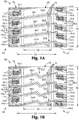
- Figures 1A and 1B illustrate an example of a top-view schematic of a portion of a printhead circuit according to the present disclosure.
- the example of the portion of the printhead circuit 100 can include a substrate 101 including a slot 102 having a first 103, a second 104, and a third dimension (e.g., 239 as illustrated in Figure 2 ) in the substrate 101.
- the printhead circuit 100 can include circuitry 105-1,105-2 on a first side surface 106 and a second side surface 107 of the slot 102.
- the printhead circuit 100 can include a number of conductor traces 108-1 through 108-N routed across the slot 102 along substantially a same geometrical plane (e.g., 238 as illustrated in Figure 2 ) as the circuitry 105-1,105-2 on the first side surface 106 and the second side surface 107 of the slot 102.
- the substrate 101 can be formed from a material selected from a group that includes gallium arsenide, ceramics, any suitable semiconducting material (e.g., a single crystalline silicon or a polycrystalline silicon), and/or combinations thereof.
- the material and/or a total thickness of the material can be chosen to achieve adequate structural support for the formation of the slot 102, a thinfilm bridge 113, and/or a fluidic layer (e.g., 229 as illustrated in Figure 2 ), as described herein.
- the thickness of the substrate 101 can be in a range of from substantially 50 microns to substantially 2000 microns (e.g., 675 microns).
- the substrate 101(201 as illustrated in Figure 2 ) can include slots formed according to the methods described herein. Additionally, in some examples, the substrate 101 can include chambers 111-1 through 111-N coupled to the slot 102. In some examples, the chambers 111-1 through 111-N and/or the slot 102 can enable fluid (e.g., ink) to be received by a number of fluid ejection elements 110-1 through 110-N, as described herein.
- fluid e.g., ink
- the slot 102 can be defined, at least in part, by the first dimension 103 and/or the second dimension 104, as illustrated in Figures 1A and 1B .
- the slot 102 can be substantially rectangular, as illustrated in Figures 1A and 1B .
- the present disclosure is not limited to such a configuration. That is, the shape of the slot 102 and/or angle of a number of walls (e.g., in the third dimension 239 as illustrated in Figure 2 ) of the slot 102, and a number, size, and configuration of the chambers 111-1 thorough 111-N, among other structural features, can be varied in a manner conducive to providing structural support for the printhead circuit 100 and/or reducing formation of bubbles in the slot 102, among other considerations.
- the slot 102 can be scalable to form a slot of a particular length (e.g., the second dimension 104) and/or a particular width (e.g., the first dimension 103).
- the first dimension 103 of the slot 102 can vary along a third dimension (e.g., 239 as illustrated in Figure 2 ) of the slot 102.
- the first dimension (e.g., 203 as illustrated in Figure 2 ) at a first substrate location can be substantially different than the first dimension (e.g., at 237 as illustrated in Figure 2 ) at a second substrate location (e.g., 235 a bottom surface of the substrate 201) of the slot 102.
- the printhead circuit 100 can include a plurality of slots, as described herein.
- the number of fluid ejection elements 110-1 through 110-N can include heat-activated (e.g., thin film resistors) and/or pressure-activated (e.g., piezoelectric) elements.
- the number of fluid ejection elements 110-1 thorough 110-N can be coupled to and/or included in a printhead circuit, as described herein.
- the thinfilm bridge 113 can be formed from a material (e.g., a thinfilm) selected from a group that includes silicon oxide formed by thermal oxidation, silicon oxide formed by chemical vapor deposition precursor Tetraethyl Orthosilicate, silicate glass formed by chemical vapor deposition containing boron and phosphorus (BPSG), chrome, tantalum, aluminum, titanium, copper, tantalum nitride, silicon nitride, silicon carbide (SiC), and/or combinations thereof.
- the thinfilm bridge 113 can connect the circuitry 105-1 on the first side surface 106 of the slot 102 to the circuitry 105-2 on the second side surface 107 of the slot 102, as described herein.
- the printhead circuit 100 includes a number of conductor traces, e.g., 108-1 thorough 108-N, in the thinfilm bridge 113 to connect the circuitry 105-1, 105-2 on the first side surface 106 and the second side of the slot 107.
- conductor traces 108-1 through 108-N in thinfilm bridges 113 provide a ground return for fluidic ejection elements 110-5 through 110-N.
- the printhead circuit 100 includes the number of conductor traces 108-1 through 108-N can multiple conductor traces in a thinfilm bridge 113. That is, a material can be provided with the thinfilm bridge 113 suitable to insulate a first conductor trace (e.g., 108-1) from a second conductor trace (not shown).
- the second conductor trace can be formed on a first surface of the first conductor trace (e.g., 108-1) with appropriate materials (e.g., dielectric) separating the same.
- the printhead circuit 100 can include forming the first conductor trace the second conductor trace from different metals. The first conductor trace and the second conductor trace may perform different functions (e.g., transport different signal types), as described herein.
- the thinfilm bridge 113 can include a number of openings 114-1 through 114-N (e.g., formed using the methods described herein).
- a combined area of the number of openings 114-1 through 114-N can be in a range of from substantially 10% to substantially 80% of an overall area (e.g., as defined by the first dimension 103 and the second dimension 104 of the slot 102) above the slot 102, as illustrated in Figures 1A and 1B .
- the shape of the number of openings 114-1 through 114-N can include substantially circular, elliptical, rectangular, triangular, rhomboidal, and/or trapezoidal, among others, depending upon a particular mask layer. As illustrated in Figures 1A and 1B , the shape and size of the number of openings 114-1 through 114-N can be substantially the same shape and size. However, the disclosure is not limited to such a configuration. That is, the shape, size, number, and configuration of the number of openings 114-1 through 114-N can be varied in a manner conducive to achieve desired properties.
- Examples of the desired properties can include promoting fluid flow in the printhead circuit 100, enabling formation of the number of conductor traces 108-1 through 108-N to pass a desired signal, reducing heat accumulation in the printhead circuit 100, and/or providing structural support for the printhead circuit 100, among other considerations.
- the number of conductor traces 108-1 through 108-N can be formed of a material that includes copper, aluminum, titanium, chrome, nickel, steel, and/or combinations thereof, among others. Accordingly, the material and/or thickness of the material can be chosen to enable transmission of the desired signal and/or contribute to mechanical flexibility of the number of conductor traces 108-1 through 108-N. In some examples, the number of conductor traces 108-1 though 108-N each can have a width in a range of from substantially 0.5 micrometers ( ⁇ m) to substantially 25 ⁇ m and a thickness in the range of 500 angstroms to 20,000 angstroms.
- the printhead circuit 100 can include a path (e.g., that of 108-1) of at least one of the number of conductor traces 108-1 though 108-N routed across the slot 102 that has a first dimension 109 greater than the first dimension 103 of the slot 102.
- the number of conductor traces 108-1 through 108-N can be routed to substantially an edge of the substrate 101. Additionally, in some examples, one or more of the number of conductor traces 108-1 through 108-N can continue beyond a first and/or a second dimensions of the substrate 101 (e.g., 108-1 as illustrated in Figures 1A and 1B ).
- the path of at least one of the number of conductor traces 108-1 though 108-N can include a direction change 199 in the path passing across the slot 102, as illustrated in Figure 1B .
- the disclosure is not limited to such a configuration. That is, the number of, and/or degree of the direction change 199 can be varied in a manner conducive to a design rule and/or a consideration, for example, transmission of electricity (e.g., the desired signal), as described herein, and/or providing a desired amount of mechanical flexibility in the number of conductor traces 108-1 though 108-N.
- the number of conductor traces 108-1 through 108-N can provide electrical connections from the first side surface 106 of the slot 102 to the number of fluid ejection elements 110-1 through 110-N on the second side surface 107 of the slot 102. In some examples, at least one of the number of conductor traces 108-1 through 108-N can conduct a control signal from the first side surface 106 of the slot 102 to a component responsive (e.g., 110) to the control signal on the second side surface 107 of the slot 102. Control signals can include status verification and/or on or off signals, among others. In some examples, the number of conductor traces 108-1 through 108-N can serve as a common ground for two or more of the number of fluid ejection elements 110-1 through 110-N, as illustrated in Figures 1A and 1B .
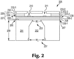
- Figure 2 illustrates an example of a side-view schematic of a portion of printhead circuit formed according to the present disclosure.
- a method of forming a printhead circuit 225 with a number of conductor traces 208 (108-1 through 108-N as illustrated in Figures 1A and 1B ) across a slot 202 can include forming a thinfilm bridge 227 on a first surface 226 of a substrate 201.
- forming the thinfilm bridge 227 can include depositing a number of thinfilm layers 230-1, 230-2, positioning the number of conductor traces (e.g., 108-1 through 108-N as illustrated in Figure 1A and 1B ) in a single plane (e.g., 238 as illustrated in Figure 2 ) across the slot 202, with the number of conductor traces (e.g., 108-1 through 108-N) having a first dimension (e.g., 109 as illustrated in Figures 1A and 1B ) greater than a predetermined first dimension 203 of the slot 202, patterning the number of thinfilm layers 230-1, 230-2, forming a fluidic layer 229 on a first surface 228 of the thinfilm bridge 227, and forming the slot 202 of the predetermined first dimension 203 in the substrate 201, as described herein.
- first dimension e.g., 109 as illustrated in Figures 1A and 1B
- Positioning the number of conductor traces (e.g., 108-1 through 108-N as illustrated in Figures 1A and 1B ) along substantially the same geometric plane (e.g., 238) as circuitry (e.g., 105 as illustrated in Figures 1A and 1B ) on a first side surface 206 and a second side surface 207 of the slot 202 can enable easier formation of the printhead circuit (e.g., 225)(e.g., reduction in the time, energy, or materials for forming), efficient (e.g., reducing energy loss during transmission) and/or reliable of transmission of electrical signals (e.g., control signals), and/or promoting a desired characteristic (e.g., flexibility) and/or configuration of the number of conductor traces 108-1 though 108-N, among other advantages.
- the printhead circuit e.g., 225
- efficient e.g., reducing energy loss during transmission
- electrical signals e.g., control signals
- the method for forming a printhead circuit 225 can include the number of conductor traces (e.g., 108-1 through 108-N as illustrated in Figures 1A and 1B ) to conduct electricity and/or control signals from the first side surface (e.g., 106) of the slot 202 to a component (not shown) responsive to the control signal on the second side surface (e.g., 107) of the slot 202.
- the first side surface e.g., 106
- a component not shown
- forming a thinfilm bridge 227 on the first surface 226 of a substrate 201 can include forming the thinfilm bridge 227 by depositing a number of thinfilm layers 230-1, 230-2 and positioning the number of conductor traces (e.g., 208) in a single plane 238 across the slot 202, such that the number of conductor traces (e.g., 208) can have a first dimension (e.g., 109 as illustrated in Figures 1A and 1B ) greater than a predetermined first dimension 203 of the slot 202.
- forming the thinfilm bridge 227 can include patterning (e.g., forming a number of openings in) the number of thinfilm layers 230-1, 230-2, as described herein.
- forming the fluidic layer 229 can include depositing and/or patterning a primer layer 231-1, 231-2 on a first surface 228 of the thinfilm bridge 227.
- forming the fluidic layer 229 can include depositing and patterning a chamber layer 232-1, 232-2 on a first surface of the primer layer 231-1, 231-2 to form a number of chambers (e.g., 211).
- the method can include depositing a wax (not shown) into the chambers (e.g., 211).
- the method can include depositing and/or patterning a nozzle layer 233-1, 233-2 on a first surface of the chamber layer 232-1, 232-2 and/or removing the wax from the number of chambers (e.g., 211). That is, the fluidic layer 229 can include the nozzle layer (e.g., 233), chamber layer (e.g., 232), and/or the primer layer (e.g., 231).
- a photo imaginable epoxy e.g., SU-8 can form a number of chambers (e.g., 211).
- the number of chambers e.g., 211) can include a number of fluid ejection elements (e.g., 210). That is, in some examples the number of fluid ejection elements (e.g., 210) can be coupled to the slot 202, for example, by one of the number of chambers (e.g., 211). Additionally, in some examples, the slot 202 and the number of fluid ejection elements (e.g., 210) can be integral.
- patterning can include forming the desired thickness, openings in, and/or shape of the thinfilm bridge 227, nozzle layer 233-1, 233-2, chamber layer 232-1, 232-2, and/or the primer layer 231-1, 231-2 using of the methods (e.g., a laser and/or a wet process etch) described herein.
- the method can include curing the primer layer 231-1, 231-2, the chamber layer 232-1, 232-2, and/or the nozzle layer 233-1, 233-2.
- curing can include heat, ultraviolet light, and/or pressure applied to the primer layer (e.g., 231), the chamber layer (e.g., 232), and/or the nozzle layer (e.g., 233).
- forming the slot 202 can include forming the slot 202 with a laser and/or etching processes (e.g., the wet process etch).
- the slot 202 can be formed utilizing any of the techniques described herein.
- the slot 202 can be formed using techniques such as sand drilling, mechanical drilling, etching, laser, an air aided laser, a water aided laser, and/or combination thereof.
- forming the slot 202 can include forming the slot with a laser, as described herein.
- forming the number of openings e.g., 114-1 through 114-N as illustrated in Figures 1A and 1B
- a laser can be either a pulse or continuous laser.
- Pulsed operation of a laser refers to any laser not classified as continuous wave (e.g., a continuous laser), so that the photons can be applied in pulses of a defined duration at a defined repetition rate.
- continuous lasers can utilize a beam whose output can be constant over time.
- the laser can control the shape, orientation, surface roughness (e.g., by removing sharp edges and/or rough material from the top and/or bottom surface of the substrate and/or from the walls of the slot 202, and/or the number of openings (e.g., 114-1 through 114-N as illustrated in Figures 1A and 1B ) in a manner conducive to reducing crack initiation and/or bubble formation sites.
- surface roughness e.g., by removing sharp edges and/or rough material from the top and/or bottom surface of the substrate and/or from the walls of the slot 202
- the number of openings e.g., 114-1 through 114-N as illustrated in Figures 1A and 1B
- Operating in pulsed and/or continuous mode can satisfy applications as described herein.
- the lasers can be multi-mode (e.g., having multiple outputs based on a variety of selectable output parameters).
- utilizing a multi-mode laser can account for various factors (e.g., the size and/or shape of the slot 202, the particular material and/or configuration of the substrate 201 among other considerations). Based on such considerations, the laser can be adjusted to emit a wavelength of a particular frequency and/or diameter.
- the laser can have a laser beam with a diameter in a range of from substantially 5 microns to substantially 100 microns.
- the laser can apply the laser beam to the substrate 201 one or a plurality of times. That is, for example, the laser beam can make multiple passes over a first portion of the substrate 201 and/or a single pass over a second portion of the substrate 201. A speed the laser beam can move over the substrate 201 and/or a focus of the beam also can be varied to achieve different results depending on the application.
- the laser can have a debris extraction system (e.g., a water-aided laser) that can remove debris resulting from laser machining.
- etching is a process for removal of one or a plurality of portions (e.g., unprotected portions) of a surface using a suitable etchant (e.g., tetramethylammonium hydroxide (TMAH), among others).
- a suitable etchant e.g., tetramethylammonium hydroxide (TMAH), among others.
- TMAH tetramethylammonium hydroxide
- the top surface 226 and/or bottom surface 235 of the substrate 201 can be exposed to an etchant sufficient to remove at least a portion of the substrate 201 material(s) to form at least a portion of the slot 202.
- etching can include patterning the thinfilm bridge 227, as described herein.
- etching can control the shape, orientation, surface roughness, and/or size of the slot 202, the number of chambers (e.g., 211) and/or from the number of openings (e.g., 114-1 through 114-N as illustrated in Figures 1A and 1B ).
- the etchant can remove sharp edges and/or rough material from the top surface and/or bottom surface 235 of the substrate and/or the number of openings (e.g., 114-1 through 114-N as illustrated in Figures 1A and 1B ). This can be conducive to reducing crack initiation and/or bubble formation sites.
- the method of forming the printhead circuit 225 can include depositing a protective layer (not shown) on a number of surfaces of the thinfilm bridge 227. That is, a layer of a material (e.g., silicon carbide) can be formed on the number of surfaces of the thinfilm bridge 227 to provide the desired properties (e.g., corrosion protection for fluid).
- the protective layer and the thinfilm bridge 227 can be integral.
- the printhead circuit can include forming a material (not shown), for example a polymer (e.g., a photo imagable polymer), on a potion of a bottom surface 235 of the substrate 202. This layer (e.g., mask) can enable masking (e.g., inhibiting etching on) a portion of the substrate 202 during etching, as described herein.
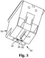
- a fluid ejection device 350 can include a housing 353 including a reservoir (not shown) for holding fluid.
- the fluid ejection 350 device can include a printhead circuit 354 affixed to the housing 353.
- the printhead circuit 350 can include a number of fluid ejection elements (e.g., 110 as illustrated in Figure 1A and 1B ) including a number of nozzles 312 operatively connected to the reservoir for ejecting fluid (e.g., ink) from the printhead circuit 354.
- the printhead circuit 354 can include a substrate (e.g., 101 as illustrated in Figure 1A and 1B ) including a slot (e.g., 102) having a first (e.g., 103), a second (e.g., 104), and a third dimension (e.g., 239 as illustrated in Figure 2 ) in the substrate (e.g., 101), circuitry (e.g., 105) on a first side surface (e.g., 106) and a second side surface (e.g., 107) of the slot (e.g., 102); and/or a number of conductor traces (e.g., 108) routed across (e.g., a path of at least one of the number of conductor traces (e.g., 108) the slot (e.g., 102) having a first dimension (e.g., 109) greater than the first dimension (e.g., 103) of the slot (e.g., 102) the slot (e.g., 10
- the fluid ejection device 350 can include the number of conductor traces (e.g., 108) having a direction change (e.g., 199 as illustrated in Figure 1B ) in a path passing across the slot (e.g., 102).
- the printhead circuit 354 and the flex circuit 352 can be bonded by the interconnect circuit 351 that can be attached (e.g., by adhesive) to the housing 353 of the fluid ejection device 350.
- the housing 353 can include an fluid (e.g., ink) reservoir (e.g., for an inkjet cartridge not shown.
- the fluid ejection device 350 can include the flex circuit 352 and/or the printhead circuit 354 configured to control the number of fluid ejection elements (e.g., 110 as illustrated in Figures 1A and 1B ) including a number of nozzles 312 that can be attached to the housing 353, the printhead circuit 354, and/or the flex circuit 352 with leads (e.g., formed of copper not shown), and a eutectic bond between each of the leads and electrical connection points (e.g., formed of gold not shown) on the printhead circuit 354 to form the interconnect circuit 351.
- the completed interconnect circuit 351 can be attached to another component as an electronic control component in an electronic device.
- the printhead circuit 354 can be configured to electronically control operation and timing of the number of fluid ejection elements (e.g., 110 as illustrated in Figures 1A and 1B )(e.g., of continuous, thermal, and piezoelectric inkjet printers, among others) that eject fluid (e.g., in the form of ink droplets) through the number of nozzles 312 of the fluid ejection device 350.
- the fluid ejection device 350 and the number of fluid ejection elements (e.g., 110 as illustrated in Figures 1A and 1B ) including the number of nozzles 312 illustrated in Figure 3 are shown by way of example and not by way of limitation.
- the fluid ejecting device 350 can be included in an inkjet cartridge. That is, the cartridges of some printing devices (e.g., inkjet printers) can each include a printhead circuit. Inkjet cartridges have various configurations, such as having color and black inks in a single cartridge, separate cartridges for black and colored inks, or a separate cartridge for black and each of the ink colors, among other configuration possibilities.
- an inkjet cartridge can have a housing 353 including a reservoir therein for holding ink and a printhead circuit affixed to the housing 353, the printhead circuit 354 having ink ejection elements (e.g., 110 as illustrated in Figures 1A and 1B ) operatively connected to the reservoir for ejecting fluid (e.g., ink) drops via the number of nozzles 312 from the printhead circuit 354.
- ink ejection elements e.g., 110 as illustrated in Figures 1A and 1B
- the term "printing device” refers to any type of printing device and/or image forming device that can employ printhead circuit(s) to achieve at least a portion of its functionality. Examples of such printing devices can include, but are not limited to, printers, facsimile machines, and/or photocopiers.
- the printhead circuit 354 can include the number of fluid ejection devices (e.g., 110) that can include the number of nozzles 312.
- the printhead circuit 354 can include a nozzle plate (not shown) including the number of nozzles 312.
- the nozzle plate can be made from an electroformed metal, a photo imageable epoxy, and/or a polyimide, among others.
- the number of nozzles 312 can be formed by any suitable method (e.g., by laser ablation).
- the nozzle plate can be integral with the primer (e.g., 231 as illustrated in Figure 2 ), chamber (e.g., 232), and/or nozzle layers (e.g., 233).
- the number of nozzles 312 can by arranged in columns or arrays along the slot (e.g., 102 as illustrated in Figures 1A and 1B ) such that properly sequenced ejection of fluid can cause characters, symbols, and/or other graphics or images to be printed on point media (e.g., as the printhead and print media are moved relative to each other).
- the print media can be any type of suitable sheet or roll material, such as paper, card stock, transparencies, Mylar, polyester, plywood, foam board, fabric, and/or canvas, among others.
- At least one of the number of conductor traces can be coupled to a drop sensing component (not shown) associated with the number of nozzles (e.g., 112).
- a conductor trace e.g., 108
- a nozzle e.g., 112
- one or more of the number of conductor traces can be divided into two sections with a space between the two sections with each section located substantially on opposing sides of the number of nozzle(s) (e.g., 112) to enable fluid (e.g., ink) drop sensing by the drop sensing component.
- fluid e.g., ink
- circuitry can include integrated circuitry (e.g., monolithic and/or hybrid integrated circuits).
- the circuitry can be formed by patterning a diffusion of a number of trace elements into and/or on a surface of a substrate (e.g., 101). Additional, in some examples, the substrate (e.g., 101) can include one or more semiconducting materials (e.g., silicon).
- the circuitry e.g., 105) can be coupled to the number of fluid ejection elements (e.g., 110) and/or the drop sensing component (not shown), among others.
- the printing device can include one or more processors.
- the processors can control various printer operations, such as media handling and/or carriage movement for linear positioning of the fluid ejecting elements (e.g., 110) over a print media (e.g., paper, transparency, etc.).
- the processors can communicate with other electronic and/or computing devices.
- the printing device can, in some examples, have an electrically erasable programmable read-only memory (EPROM), read-only memory (ROM), and/or a random access memory (RAM).
- the memory components e.g., EPROM, ROM, and/or RAM
- can store various information and/or data such as configuration information, fonts, templates, data being printed, and/or menu structure information.
- a printing device can also include a flash memory device in place of or in addition to the memory components (e.g., EPROM).
- a system bus can connect the various components (e.g., EPROM) within the printing device.
- the printing device can, in some examples, have a firmware component that can be implemented as a permanent memory module stored in memory (e.g., ROM).
- the firmware can be programmed and/or tested like software.
- the firmware can be distributed along with the printing device to enable implementing and/or coordinating operations of the hardware within printing device and/or contain programming constructs used to perform such operations.
- the printhead circuit can include the plurality of slots in the substrate.
- the number of conductor traces can pass over two or more slots.
- the plurality of the slots can be coupled to a single fluid supply, as described herein. Alternatively, the plurality of slots can divide the fluid supply so that each of the plurality of slots receives a separate fluid supply.
- the present disclosure includes apparatuses and methods for implementing a printhead circuit.
- Printhead circuits can be used for the applications described in the present disclosure, although the printhead circuits are not limited to such applications. It is to be understood that the above description has been made in an illustrative fashion and not a restrictive one. Although specific examples for apparatuses and methods have been illustrated and described herein, other equivalent component arrangements and/or structures conducive to structural support of the printhead circuits and/or efficient printing can be substituted for the specific examples shown herein.
Landscapes
- Engineering & Computer Science (AREA)
- Manufacturing & Machinery (AREA)
- Microelectronics & Electronic Packaging (AREA)
- Particle Formation And Scattering Control In Inkjet Printers (AREA)
Claims (14)
- Druckkopfschaltung (100, 225, 354), die Folgendes umfasst:ein Substrat (101, 201) einschließlich eines Schlitzes (102, 202) mit einer ersten (103), einer zweiten (104) und einer dritten (239) Abmessung in dem Substrat (101, 201);eine Schaltungsanordnung (105) auf einer ersten Seite (106, 206) und einer zweiten Seite (107, 207) des Schlitzes (102, 202), wobei die Schaltungsanordnung (105) wenigstens Fluidausstoßelemente (110, 210) umfasst; undeine Anzahl von Leiterbahnen (108, 208) in einer Dünnfilmbrücke (113, 227), die auf einer ersten Oberfläche (226) des Substrats (101, 201) ausgebildet sind und über den Schlitz (102, 202) entlang einer im Wesentlichen gleichen geometrischen Ebene (238) wie die Schaltungsanordnung (105) auf der ersten Seite (106, 206) und der zweiten Seite (107, 207) des Schlitzes (102, 202) geleitet sind, wodurch die Dünnfilmbrücke (113, 227) die Schaltungsanordnung (105) auf der ersten Seite (106, 206) und der zweiten Seite (107, 207) des Schlitzes (102, 202) verbindet.
- Druckkopfschaltung nach Anspruch 1, die einen Pfad von wenigstens einer der Anzahl von Leiterbahnen (108, 208), die über den Schlitz (102, 202) geleitet sind, umfasst, mit einer ersten Abmessung (109), die größer als die erste Abmessung (103) des Schlitzes (102, 202) ist.
- Druckkopfschaltung nach Anspruch 2, wobei der Pfad von wenigstens einer der Anzahl von Leiterbahnen (108, 208) eine Richtungsänderung (199) in dem Pfad, der über den Schlitz (102, 202) verläuft, umfasst.
- Druckkopfschaltung nach Anspruch 1, wobei die Anzahl von Leiterbahnen (108, 208) jeweils eine Breite in einem Bereich von im Wesentlichen 0,5 Mikrometer (µm) bis im Wesentlichen 25 µm aufweist.
- Druckkopfschaltung nach Anspruch 1, wobei die Anzahl von Leiterbahnen (108, 208) eine erste Leiterbahn und eine zweite Leiterbahn umfasst, wobei ein Dünnfilm auf einer ersten Oberfläche der ersten Leiterbahn ausgebildet ist und die zweite Leiterbahn auf einer ersten Oberfläche des Dünnfilms ausgebildet ist, wodurch der Dünnfilm die Dünnfilmbrücke ausbildet.
- Druckkopfschaltung nach Anspruch 5, wobei die erste Leiterbahn und die zweite Leiterbahn aus unterschiedlichen Metallen ausgebildet sind.
- Druckkopfschaltung nach Anspruch 1, wobei die Dünnfilmbrücke (113, 227) eine Anzahl von Öffnungen (114) einschließt, die einen kombinierten Bereich der Anzahl von Öffnungen (114) in einem Bereich von im Wesentlichen 10 % bis im Wesentlichen 80 % eines Gesamtbereichs über dem Schlitz (102, 202) umfassen.
- Fluidausstoßvorrichtung (350), die Folgendes umfasst:ein Gehäuse (353), das einen Behälter zum Enthalten von Fluid einschließt;eine Druckkopfschaltung (100, 225, 354) nach einem der Ansprüche 1 bis 7, die an dem Gehäuse (353) befestigt ist; und wodurch die Anzahl von Fluidausstoßelementen (110, 210) eine Anzahl von Düsen (112, 312) einschließt, die mit dem Behälter wirkverbunden sind, um Fluid aus der Druckkopfschaltung (100, 225, 354) auszustoßen.
- Vorrichtung nach Anspruch 8, wobei die Anzahl von Leiterbahnen (108, 208) eine Richtungsänderung (199) in einem Pfad aufweisen, der über den Schlitz (102, 202) verläuft.
- Verfahren zum Ausbilden einer Druckkopfschaltung (100, 225, 354) mit einer Anzahl von Leiterbahnen (108, 208) über einen Schlitz (102, 202), das Folgendes umfasst:
Ausbilden einer Dünnfilmbrücke (113, 227) auf einer ersten Oberfläche (226) eines Substrats (101, 201), wobei das Ausbilden der Dünnfilmbrücke (113, 227) Folgendes umfasst:Abscheiden einer Anzahl von Dünnfilmschichten (230);Positionieren der Anzahl von Leiterbahnen (108, 208) in der Anzahl von Dünnfilmschichten (230) entlang einer im Wesentlichen gleichen geometrischen Ebene (238) wie eine Schaltungsanordnung (105) auf einer ersten Seite (106, 206) und einer zweiten Seite (107, 207) des Schlitzes (102, 202), wobei die Schaltungsanordnung (105) wenigstens Fluidausstoßelemente (110, 210) umfasst, wobei die Anzahl von Leiterbahnen (108, 208) eine erste Abmessung (109) aufweist, die größer als eine vorbestimmte erste Abmessung (103) des Schlitzes (102, 202) ist;Strukturieren der Anzahl von Dünnfilmschichten (230);Ausbilden einer fluidischen Schicht (229) auf einer ersten Oberfläche (228) der Dünnfilmbrücke (113, 227) undAusbilden des Schlitzes (102, 202) der vorbestimmten ersten Abmessung (103) in dem Substrat (101, 201). - Verfahren nach Anspruch 10, wobei wenigstens eine der Anzahl von Leiterbahnen (108, 208) elektrische Verbindungen von der ersten Seite (106, 206) des Schlitzes (102, 202) einer Anzahl von Fluidausstoßvorrichtungen auf der zweiten Seite (107, 207) des Schlitzes (102, 202) bereitstellt.
- Verfahren nach Anspruch 10, wobei wenigstens eine der Anzahl von Leiterbahnen (108, 208) Steuersignale von der ersten Seite (106, 206) des Schlitzes (102, 202) zu einer Komponente, die auf das Steuersignal auf der zweiten Seite (107, 207) des Schlitzes (102, 202) anspricht, leitet.
- Verfahren nach Anspruch 10, wobei das Ausbilden des Schlitzes (102, 202) ein Ausbilden des Schlitzes (102, 202) unter Verwendung einer Laser- und Nassverfahrensätzung umfasst.
- Verfahren nach Anspruch 10, wobei das Verfahren ein Abscheiden einer Schutzschicht auf einer Anzahl von Oberflächen der Dünnfilmschichten (230) einschließt.
Applications Claiming Priority (1)
| Application Number | Priority Date | Filing Date | Title |
|---|---|---|---|
| PCT/US2012/040161 WO2013180715A1 (en) | 2012-05-31 | 2012-05-31 | Printheads with conductor traces across slots |
Publications (3)
| Publication Number | Publication Date |
|---|---|
| EP2828086A1 EP2828086A1 (de) | 2015-01-28 |
| EP2828086A4 EP2828086A4 (de) | 2016-10-19 |
| EP2828086B1 true EP2828086B1 (de) | 2019-09-11 |
Family
ID=49673763
Family Applications (1)
| Application Number | Title | Priority Date | Filing Date |
|---|---|---|---|
| EP12877853.7A Active EP2828086B1 (de) | 2012-05-31 | 2012-05-31 | Druckköpfe mit leiterspuren durch schlitze |
Country Status (4)
| Country | Link |
|---|---|
| US (1) | US20150145925A1 (de) |
| EP (1) | EP2828086B1 (de) |
| CN (1) | CN104245329B (de) |
| WO (1) | WO2013180715A1 (de) |
Cited By (1)
| Publication number | Priority date | Publication date | Assignee | Title |
|---|---|---|---|---|
| WO2025136355A1 (en) * | 2023-12-18 | 2025-06-26 | Hewlett-Packard Development Company, L.P. | Protrusions into a fluid passage opening |
Families Citing this family (6)
| Publication number | Priority date | Publication date | Assignee | Title |
|---|---|---|---|---|
| US10427407B2 (en) | 2014-03-31 | 2019-10-01 | Hewlett-Packard Development Company, L.P. | Printer circuit board fluid ejection apparatus |
| PL3710260T3 (pl) | 2019-02-06 | 2021-12-06 | Hewlett-Packard Development Company, L.P. | Matryca do głowicy drukującej |
| CN113365842B (zh) | 2019-02-06 | 2022-10-14 | 惠普发展公司,有限责任合伙企业 | 流体喷射装置和制造流体喷射装置的方法 |
| CN113543978B (zh) | 2019-02-06 | 2023-06-30 | 惠普发展公司,有限责任合伙企业 | 打印头的管芯、打印头和形成打印头的管芯的方法 |
| WO2020162924A1 (en) * | 2019-02-06 | 2020-08-13 | Hewlett-Packard Development Company, L.P. | Die for a printhead |
| MX2021009368A (es) | 2019-02-06 | 2021-09-10 | Hewlett Packard Development Co | Matriz para un cabezal de impresion. |
Family Cites Families (19)
| Publication number | Priority date | Publication date | Assignee | Title |
|---|---|---|---|---|
| US4827294A (en) * | 1985-11-22 | 1989-05-02 | Hewlett-Packard Company | Thermal ink jet printhead assembly employing beam lead interconnect circuit |
| US6336714B1 (en) * | 1996-02-07 | 2002-01-08 | Hewlett-Packard Company | Fully integrated thermal inkjet printhead having thin film layer shelf |
| US5953032A (en) * | 1997-06-10 | 1999-09-14 | Lexmark International, Inc. | Method for forming and inspecting a barrier layer of an ink jet print cartridge |
| US6019907A (en) | 1997-08-08 | 2000-02-01 | Hewlett-Packard Company | Forming refill for monolithic inkjet printhead |
| US6065823A (en) * | 1999-04-16 | 2000-05-23 | Hewlett-Packard Company | Heat spreader for ink-jet printhead |
| TW446644B (en) * | 2000-01-29 | 2001-07-21 | Ind Tech Res Inst | Method and structure for precise temperature measurement of ink-jet printhead heating element |
| US6482574B1 (en) * | 2000-04-20 | 2002-11-19 | Hewlett-Packard Co. | Droplet plate architecture in ink-jet printheads |
| KR100408269B1 (ko) | 2000-07-20 | 2003-12-01 | 삼성전자주식회사 | 잉크제트 프린트헤드 |
| US6457815B1 (en) * | 2001-01-29 | 2002-10-01 | Hewlett-Packard Company | Fluid-jet printhead and method of fabricating a fluid-jet printhead |
| KR100419217B1 (ko) * | 2001-11-02 | 2004-02-19 | 삼성전자주식회사 | 단판 잉크젯 프린트 헤드 및 그 제조방법 |
| KR100641357B1 (ko) * | 2004-08-26 | 2006-11-01 | 삼성전자주식회사 | 잉크젯 프린트 헤드 및 그 제조 방법 |
| US7946690B2 (en) * | 2007-02-20 | 2011-05-24 | Mvm Technologies, Inc. | Printhead fabricated on flexible substrate |
| US8197030B1 (en) * | 2008-03-10 | 2012-06-12 | Hewlett-Packard Development Company, L.P. | Fluid ejector structure |
| US8733902B2 (en) * | 2008-05-06 | 2014-05-27 | Hewlett-Packard Development Company, L.P. | Printhead feed slot ribs |
| KR101256855B1 (ko) * | 2008-05-22 | 2013-04-22 | 후지필름 가부시키가이샤 | 다이와 집적 회로 소자를 갖는 액추에이팅 가능한 장치 |
| WO2010044775A1 (en) * | 2008-10-14 | 2010-04-22 | Hewlett-Packard Development Company, L.P. | Fluid ejector structure |
| CN102574397A (zh) * | 2009-10-08 | 2012-07-11 | 惠普发展公司,有限责任合伙企业 | 具有跨槽导体布线的喷墨打印头 |
| US8585187B2 (en) * | 2011-04-29 | 2013-11-19 | Xerox Corporation | High density electrical interconnect for printing devices using flex circuits and dielectric underfill |
| US8857021B2 (en) * | 2012-06-15 | 2014-10-14 | Xerox Corporation | Laser welded bonding pads for piezoelectric print heads |
-
2012
- 2012-05-31 US US14/396,161 patent/US20150145925A1/en not_active Abandoned
- 2012-05-31 CN CN201280072869.6A patent/CN104245329B/zh not_active Expired - Fee Related
- 2012-05-31 WO PCT/US2012/040161 patent/WO2013180715A1/en not_active Ceased
- 2012-05-31 EP EP12877853.7A patent/EP2828086B1/de active Active
Non-Patent Citations (1)
| Title |
|---|
| None * |
Cited By (1)
| Publication number | Priority date | Publication date | Assignee | Title |
|---|---|---|---|---|
| WO2025136355A1 (en) * | 2023-12-18 | 2025-06-26 | Hewlett-Packard Development Company, L.P. | Protrusions into a fluid passage opening |
Also Published As
| Publication number | Publication date |
|---|---|
| EP2828086A1 (de) | 2015-01-28 |
| WO2013180715A1 (en) | 2013-12-05 |
| CN104245329B (zh) | 2016-03-02 |
| US20150145925A1 (en) | 2015-05-28 |
| CN104245329A (zh) | 2014-12-24 |
| EP2828086A4 (de) | 2016-10-19 |
Similar Documents
| Publication | Publication Date | Title |
|---|---|---|
| EP2828086B1 (de) | Druckköpfe mit leiterspuren durch schlitze | |
| US9573369B2 (en) | Fluid ejection assembly with controlled adhesive bond | |
| EP2828081B1 (de) | Flüssigkeitsausstossvorrichtung mit partikeltoleranter dünnfilmverlängerung | |
| US10479080B2 (en) | Fluid ejection device with ink feedhole bridge | |
| CN104853923B (zh) | 具有颗粒耐受层延伸部的流体喷射装置 | |
| US20120019597A1 (en) | Inkjet printhead with cross-slot conductor routing | |
| JP2008179039A (ja) | 液体吐出ヘッド及び液体吐出ヘッドの製造方法 | |
| US10369788B2 (en) | Printhead with recessed slot ends | |
| US10449762B2 (en) | Fluid ejection device | |
| EP2817154A1 (de) | Flüssigkeitsausstossvorrichtung | |
| US9895885B2 (en) | Fluid ejection device with particle tolerant layer extension | |
| CN110446613B (zh) | 模制到模制主体中的流体喷射管芯 | |
| HK40012778A (en) | Fluid ejection die molded into molded body | |
| HK40012778B (en) | Fluid ejection die molded into molded body |
Legal Events
| Date | Code | Title | Description |
|---|---|---|---|
| PUAI | Public reference made under article 153(3) epc to a published international application that has entered the european phase |
Free format text: ORIGINAL CODE: 0009012 |
|
| 17P | Request for examination filed |
Effective date: 20141021 |
|
| AK | Designated contracting states |
Kind code of ref document: A1 Designated state(s): AL AT BE BG CH CY CZ DE DK EE ES FI FR GB GR HR HU IE IS IT LI LT LU LV MC MK MT NL NO PL PT RO RS SE SI SK SM TR |
|
| AX | Request for extension of the european patent |
Extension state: BA ME |
|
| DAX | Request for extension of the european patent (deleted) | ||
| RA4 | Supplementary search report drawn up and despatched (corrected) |
Effective date: 20160915 |
|
| RIC1 | Information provided on ipc code assigned before grant |
Ipc: H05K 3/10 20060101ALI20160909BHEP Ipc: B41J 2/175 20060101AFI20160909BHEP Ipc: B41J 2/045 20060101ALI20160909BHEP Ipc: B41J 2/14 20060101ALI20160909BHEP |
|
| STAA | Information on the status of an ep patent application or granted ep patent |
Free format text: STATUS: EXAMINATION IS IN PROGRESS |
|
| 17Q | First examination report despatched |
Effective date: 20180813 |
|
| GRAP | Despatch of communication of intention to grant a patent |
Free format text: ORIGINAL CODE: EPIDOSNIGR1 |
|
| STAA | Information on the status of an ep patent application or granted ep patent |
Free format text: STATUS: GRANT OF PATENT IS INTENDED |
|
| INTG | Intention to grant announced |
Effective date: 20190405 |
|
| RAP1 | Party data changed (applicant data changed or rights of an application transferred) |
Owner name: HEWLETT-PACKARD DEVELOPMENT COMPANY, L.P. |
|
| GRAS | Grant fee paid |
Free format text: ORIGINAL CODE: EPIDOSNIGR3 |
|
| GRAA | (expected) grant |
Free format text: ORIGINAL CODE: 0009210 |
|
| STAA | Information on the status of an ep patent application or granted ep patent |
Free format text: STATUS: THE PATENT HAS BEEN GRANTED |
|
| AK | Designated contracting states |
Kind code of ref document: B1 Designated state(s): AL AT BE BG CH CY CZ DE DK EE ES FI FR GB GR HR HU IE IS IT LI LT LU LV MC MK MT NL NO PL PT RO RS SE SI SK SM TR |
|
| REG | Reference to a national code |
Ref country code: GB Ref legal event code: FG4D |
|
| REG | Reference to a national code |
Ref country code: CH Ref legal event code: EP |
|
| REG | Reference to a national code |
Ref country code: AT Ref legal event code: REF Ref document number: 1177932 Country of ref document: AT Kind code of ref document: T Effective date: 20190915 |
|
| REG | Reference to a national code |
Ref country code: DE Ref legal event code: R096 Ref document number: 602012064005 Country of ref document: DE |
|
| REG | Reference to a national code |
Ref country code: IE Ref legal event code: FG4D |
|
| REG | Reference to a national code |
Ref country code: NL Ref legal event code: MP Effective date: 20190911 |
|
| REG | Reference to a national code |
Ref country code: LT Ref legal event code: MG4D |
|
| PG25 | Lapsed in a contracting state [announced via postgrant information from national office to epo] |
Ref country code: BG Free format text: LAPSE BECAUSE OF FAILURE TO SUBMIT A TRANSLATION OF THE DESCRIPTION OR TO PAY THE FEE WITHIN THE PRESCRIBED TIME-LIMIT Effective date: 20191211 Ref country code: SE Free format text: LAPSE BECAUSE OF FAILURE TO SUBMIT A TRANSLATION OF THE DESCRIPTION OR TO PAY THE FEE WITHIN THE PRESCRIBED TIME-LIMIT Effective date: 20190911 Ref country code: HR Free format text: LAPSE BECAUSE OF FAILURE TO SUBMIT A TRANSLATION OF THE DESCRIPTION OR TO PAY THE FEE WITHIN THE PRESCRIBED TIME-LIMIT Effective date: 20190911 Ref country code: LT Free format text: LAPSE BECAUSE OF FAILURE TO SUBMIT A TRANSLATION OF THE DESCRIPTION OR TO PAY THE FEE WITHIN THE PRESCRIBED TIME-LIMIT Effective date: 20190911 Ref country code: FI Free format text: LAPSE BECAUSE OF FAILURE TO SUBMIT A TRANSLATION OF THE DESCRIPTION OR TO PAY THE FEE WITHIN THE PRESCRIBED TIME-LIMIT Effective date: 20190911 Ref country code: NO Free format text: LAPSE BECAUSE OF FAILURE TO SUBMIT A TRANSLATION OF THE DESCRIPTION OR TO PAY THE FEE WITHIN THE PRESCRIBED TIME-LIMIT Effective date: 20191211 |
|
| PG25 | Lapsed in a contracting state [announced via postgrant information from national office to epo] |
Ref country code: AL Free format text: LAPSE BECAUSE OF FAILURE TO SUBMIT A TRANSLATION OF THE DESCRIPTION OR TO PAY THE FEE WITHIN THE PRESCRIBED TIME-LIMIT Effective date: 20190911 Ref country code: ES Free format text: LAPSE BECAUSE OF FAILURE TO SUBMIT A TRANSLATION OF THE DESCRIPTION OR TO PAY THE FEE WITHIN THE PRESCRIBED TIME-LIMIT Effective date: 20190911 Ref country code: LV Free format text: LAPSE BECAUSE OF FAILURE TO SUBMIT A TRANSLATION OF THE DESCRIPTION OR TO PAY THE FEE WITHIN THE PRESCRIBED TIME-LIMIT Effective date: 20190911 Ref country code: GR Free format text: LAPSE BECAUSE OF FAILURE TO SUBMIT A TRANSLATION OF THE DESCRIPTION OR TO PAY THE FEE WITHIN THE PRESCRIBED TIME-LIMIT Effective date: 20191212 Ref country code: RS Free format text: LAPSE BECAUSE OF FAILURE TO SUBMIT A TRANSLATION OF THE DESCRIPTION OR TO PAY THE FEE WITHIN THE PRESCRIBED TIME-LIMIT Effective date: 20190911 |
|
| REG | Reference to a national code |
Ref country code: AT Ref legal event code: MK05 Ref document number: 1177932 Country of ref document: AT Kind code of ref document: T Effective date: 20190911 |
|
| PG25 | Lapsed in a contracting state [announced via postgrant information from national office to epo] |
Ref country code: PT Free format text: LAPSE BECAUSE OF FAILURE TO SUBMIT A TRANSLATION OF THE DESCRIPTION OR TO PAY THE FEE WITHIN THE PRESCRIBED TIME-LIMIT Effective date: 20200113 Ref country code: RO Free format text: LAPSE BECAUSE OF FAILURE TO SUBMIT A TRANSLATION OF THE DESCRIPTION OR TO PAY THE FEE WITHIN THE PRESCRIBED TIME-LIMIT Effective date: 20190911 Ref country code: IT Free format text: LAPSE BECAUSE OF FAILURE TO SUBMIT A TRANSLATION OF THE DESCRIPTION OR TO PAY THE FEE WITHIN THE PRESCRIBED TIME-LIMIT Effective date: 20190911 Ref country code: AT Free format text: LAPSE BECAUSE OF FAILURE TO SUBMIT A TRANSLATION OF THE DESCRIPTION OR TO PAY THE FEE WITHIN THE PRESCRIBED TIME-LIMIT Effective date: 20190911 Ref country code: PL Free format text: LAPSE BECAUSE OF FAILURE TO SUBMIT A TRANSLATION OF THE DESCRIPTION OR TO PAY THE FEE WITHIN THE PRESCRIBED TIME-LIMIT Effective date: 20190911 Ref country code: EE Free format text: LAPSE BECAUSE OF FAILURE TO SUBMIT A TRANSLATION OF THE DESCRIPTION OR TO PAY THE FEE WITHIN THE PRESCRIBED TIME-LIMIT Effective date: 20190911 Ref country code: NL Free format text: LAPSE BECAUSE OF FAILURE TO SUBMIT A TRANSLATION OF THE DESCRIPTION OR TO PAY THE FEE WITHIN THE PRESCRIBED TIME-LIMIT Effective date: 20190911 |
|
| PG25 | Lapsed in a contracting state [announced via postgrant information from national office to epo] |
Ref country code: IS Free format text: LAPSE BECAUSE OF FAILURE TO SUBMIT A TRANSLATION OF THE DESCRIPTION OR TO PAY THE FEE WITHIN THE PRESCRIBED TIME-LIMIT Effective date: 20200224 Ref country code: SK Free format text: LAPSE BECAUSE OF FAILURE TO SUBMIT A TRANSLATION OF THE DESCRIPTION OR TO PAY THE FEE WITHIN THE PRESCRIBED TIME-LIMIT Effective date: 20190911 Ref country code: SM Free format text: LAPSE BECAUSE OF FAILURE TO SUBMIT A TRANSLATION OF THE DESCRIPTION OR TO PAY THE FEE WITHIN THE PRESCRIBED TIME-LIMIT Effective date: 20190911 Ref country code: CZ Free format text: LAPSE BECAUSE OF FAILURE TO SUBMIT A TRANSLATION OF THE DESCRIPTION OR TO PAY THE FEE WITHIN THE PRESCRIBED TIME-LIMIT Effective date: 20190911 |
|
| REG | Reference to a national code |
Ref country code: DE Ref legal event code: R097 Ref document number: 602012064005 Country of ref document: DE |
|
| PLBE | No opposition filed within time limit |
Free format text: ORIGINAL CODE: 0009261 |
|
| STAA | Information on the status of an ep patent application or granted ep patent |
Free format text: STATUS: NO OPPOSITION FILED WITHIN TIME LIMIT |
|
| PG2D | Information on lapse in contracting state deleted |
Ref country code: IS |
|
| PG25 | Lapsed in a contracting state [announced via postgrant information from national office to epo] |
Ref country code: DK Free format text: LAPSE BECAUSE OF FAILURE TO SUBMIT A TRANSLATION OF THE DESCRIPTION OR TO PAY THE FEE WITHIN THE PRESCRIBED TIME-LIMIT Effective date: 20190911 Ref country code: IS Free format text: LAPSE BECAUSE OF FAILURE TO SUBMIT A TRANSLATION OF THE DESCRIPTION OR TO PAY THE FEE WITHIN THE PRESCRIBED TIME-LIMIT Effective date: 20200112 |
|
| 26N | No opposition filed |
Effective date: 20200615 |
|
| PG25 | Lapsed in a contracting state [announced via postgrant information from national office to epo] |
Ref country code: SI Free format text: LAPSE BECAUSE OF FAILURE TO SUBMIT A TRANSLATION OF THE DESCRIPTION OR TO PAY THE FEE WITHIN THE PRESCRIBED TIME-LIMIT Effective date: 20190911 |
|
| PG25 | Lapsed in a contracting state [announced via postgrant information from national office to epo] |
Ref country code: LI Free format text: LAPSE BECAUSE OF NON-PAYMENT OF DUE FEES Effective date: 20200531 Ref country code: CH Free format text: LAPSE BECAUSE OF NON-PAYMENT OF DUE FEES Effective date: 20200531 Ref country code: MC Free format text: LAPSE BECAUSE OF FAILURE TO SUBMIT A TRANSLATION OF THE DESCRIPTION OR TO PAY THE FEE WITHIN THE PRESCRIBED TIME-LIMIT Effective date: 20190911 |
|
| REG | Reference to a national code |
Ref country code: BE Ref legal event code: MM Effective date: 20200531 |
|
| GBPC | Gb: european patent ceased through non-payment of renewal fee |
Effective date: 20200531 |
|
| PG25 | Lapsed in a contracting state [announced via postgrant information from national office to epo] |
Ref country code: LU Free format text: LAPSE BECAUSE OF NON-PAYMENT OF DUE FEES Effective date: 20200531 |
|
| PG25 | Lapsed in a contracting state [announced via postgrant information from national office to epo] |
Ref country code: FR Free format text: LAPSE BECAUSE OF NON-PAYMENT OF DUE FEES Effective date: 20200531 Ref country code: GB Free format text: LAPSE BECAUSE OF NON-PAYMENT OF DUE FEES Effective date: 20200531 Ref country code: IE Free format text: LAPSE BECAUSE OF NON-PAYMENT OF DUE FEES Effective date: 20200531 |
|
| PG25 | Lapsed in a contracting state [announced via postgrant information from national office to epo] |
Ref country code: BE Free format text: LAPSE BECAUSE OF NON-PAYMENT OF DUE FEES Effective date: 20200531 |
|
| PG25 | Lapsed in a contracting state [announced via postgrant information from national office to epo] |
Ref country code: TR Free format text: LAPSE BECAUSE OF FAILURE TO SUBMIT A TRANSLATION OF THE DESCRIPTION OR TO PAY THE FEE WITHIN THE PRESCRIBED TIME-LIMIT Effective date: 20190911 Ref country code: MT Free format text: LAPSE BECAUSE OF FAILURE TO SUBMIT A TRANSLATION OF THE DESCRIPTION OR TO PAY THE FEE WITHIN THE PRESCRIBED TIME-LIMIT Effective date: 20190911 Ref country code: CY Free format text: LAPSE BECAUSE OF FAILURE TO SUBMIT A TRANSLATION OF THE DESCRIPTION OR TO PAY THE FEE WITHIN THE PRESCRIBED TIME-LIMIT Effective date: 20190911 |
|
| PG25 | Lapsed in a contracting state [announced via postgrant information from national office to epo] |
Ref country code: MK Free format text: LAPSE BECAUSE OF FAILURE TO SUBMIT A TRANSLATION OF THE DESCRIPTION OR TO PAY THE FEE WITHIN THE PRESCRIBED TIME-LIMIT Effective date: 20190911 |
|
| PGFP | Annual fee paid to national office [announced via postgrant information from national office to epo] |
Ref country code: DE Payment date: 20210716 Year of fee payment: 11 |
|
| REG | Reference to a national code |
Ref country code: DE Ref legal event code: R119 Ref document number: 602012064005 Country of ref document: DE |
|
| PG25 | Lapsed in a contracting state [announced via postgrant information from national office to epo] |
Ref country code: DE Free format text: LAPSE BECAUSE OF NON-PAYMENT OF DUE FEES Effective date: 20231201 |