EP2827686A1 - Flexible printed circuit film and display device including the same - Google Patents
Flexible printed circuit film and display device including the same Download PDFInfo
- Publication number
- EP2827686A1 EP2827686A1 EP14161398.4A EP14161398A EP2827686A1 EP 2827686 A1 EP2827686 A1 EP 2827686A1 EP 14161398 A EP14161398 A EP 14161398A EP 2827686 A1 EP2827686 A1 EP 2827686A1
- Authority
- EP
- European Patent Office
- Prior art keywords
- printed circuit
- flexible printed
- cover layer
- bending region
- circuit film
- Prior art date
- Legal status (The legal status is an assumption and is not a legal conclusion. Google has not performed a legal analysis and makes no representation as to the accuracy of the status listed.)
- Withdrawn
Links
- 238000005452 bending Methods 0.000 claims abstract description 78
- 239000000758 substrate Substances 0.000 claims abstract description 58
- 238000005538 encapsulation Methods 0.000 claims description 9
- 239000000463 material Substances 0.000 description 4
- 239000000565 sealant Substances 0.000 description 3
- 239000004593 Epoxy Substances 0.000 description 2
- UQSXHKLRYXJYBZ-UHFFFAOYSA-N Iron oxide Chemical compound [Fe]=O UQSXHKLRYXJYBZ-UHFFFAOYSA-N 0.000 description 2
- 239000000853 adhesive Substances 0.000 description 2
- 230000001070 adhesive effect Effects 0.000 description 2
- TWNQGVIAIRXVLR-UHFFFAOYSA-N oxo(oxoalumanyloxy)alumane Chemical compound O=[Al]O[Al]=O TWNQGVIAIRXVLR-UHFFFAOYSA-N 0.000 description 2
- XLOMVQKBTHCTTD-UHFFFAOYSA-N Zinc monoxide Chemical compound [Zn]=O XLOMVQKBTHCTTD-UHFFFAOYSA-N 0.000 description 1
- GHPGOEFPKIHBNM-UHFFFAOYSA-N antimony(3+);oxygen(2-) Chemical compound [O-2].[O-2].[O-2].[Sb+3].[Sb+3] GHPGOEFPKIHBNM-UHFFFAOYSA-N 0.000 description 1
- 239000000919 ceramic Substances 0.000 description 1
- JKWMSGQKBLHBQQ-UHFFFAOYSA-N diboron trioxide Chemical compound O=BOB=O JKWMSGQKBLHBQQ-UHFFFAOYSA-N 0.000 description 1
- FZFYOUJTOSBFPQ-UHFFFAOYSA-M dipotassium;hydroxide Chemical compound [OH-].[K+].[K+] FZFYOUJTOSBFPQ-UHFFFAOYSA-M 0.000 description 1
- GNTDGMZSJNCJKK-UHFFFAOYSA-N divanadium pentaoxide Chemical compound O=[V](=O)O[V](=O)=O GNTDGMZSJNCJKK-UHFFFAOYSA-N 0.000 description 1
- 239000011521 glass Substances 0.000 description 1
- 239000004973 liquid crystal related substance Substances 0.000 description 1
- 239000011159 matrix material Substances 0.000 description 1
- 238000000034 method Methods 0.000 description 1
- 239000000203 mixture Substances 0.000 description 1
- 238000012986 modification Methods 0.000 description 1
- 230000004048 modification Effects 0.000 description 1
- YEXPOXQUZXUXJW-UHFFFAOYSA-N oxolead Chemical compound [Pb]=O YEXPOXQUZXUXJW-UHFFFAOYSA-N 0.000 description 1
- 230000002093 peripheral effect Effects 0.000 description 1
- 239000004033 plastic Substances 0.000 description 1
- 239000010453 quartz Substances 0.000 description 1
- VYPSYNLAJGMNEJ-UHFFFAOYSA-N silicon dioxide Inorganic materials O=[Si]=O VYPSYNLAJGMNEJ-UHFFFAOYSA-N 0.000 description 1
- DLYUQMMRRRQYAE-UHFFFAOYSA-N tetraphosphorus decaoxide Chemical compound O1P(O2)(=O)OP3(=O)OP1(=O)OP2(=O)O3 DLYUQMMRRRQYAE-UHFFFAOYSA-N 0.000 description 1
- XOLBLPGZBRYERU-UHFFFAOYSA-N tin dioxide Chemical compound O=[Sn]=O XOLBLPGZBRYERU-UHFFFAOYSA-N 0.000 description 1
- 229910001887 tin oxide Inorganic materials 0.000 description 1
- ZNOKGRXACCSDPY-UHFFFAOYSA-N tungsten trioxide Chemical compound O=[W](=O)=O ZNOKGRXACCSDPY-UHFFFAOYSA-N 0.000 description 1
Images

Classifications
-
- H—ELECTRICITY
- H05—ELECTRIC TECHNIQUES NOT OTHERWISE PROVIDED FOR
- H05K—PRINTED CIRCUITS; CASINGS OR CONSTRUCTIONAL DETAILS OF ELECTRIC APPARATUS; MANUFACTURE OF ASSEMBLAGES OF ELECTRICAL COMPONENTS
- H05K7/00—Constructional details common to different types of electric apparatus
-
- G—PHYSICS
- G09—EDUCATION; CRYPTOGRAPHY; DISPLAY; ADVERTISING; SEALS
- G09F—DISPLAYING; ADVERTISING; SIGNS; LABELS OR NAME-PLATES; SEALS
- G09F9/00—Indicating arrangements for variable information in which the information is built-up on a support by selection or combination of individual elements
-
- H—ELECTRICITY
- H05—ELECTRIC TECHNIQUES NOT OTHERWISE PROVIDED FOR
- H05K—PRINTED CIRCUITS; CASINGS OR CONSTRUCTIONAL DETAILS OF ELECTRIC APPARATUS; MANUFACTURE OF ASSEMBLAGES OF ELECTRICAL COMPONENTS
- H05K1/00—Printed circuits
- H05K1/02—Details
- H05K1/0277—Bendability or stretchability details
- H05K1/028—Bending or folding regions of flexible printed circuits
-
- H—ELECTRICITY
- H05—ELECTRIC TECHNIQUES NOT OTHERWISE PROVIDED FOR
- H05K—PRINTED CIRCUITS; CASINGS OR CONSTRUCTIONAL DETAILS OF ELECTRIC APPARATUS; MANUFACTURE OF ASSEMBLAGES OF ELECTRICAL COMPONENTS
- H05K1/00—Printed circuits
- H05K1/02—Details
- H05K1/0277—Bendability or stretchability details
- H05K1/028—Bending or folding regions of flexible printed circuits
- H05K1/0281—Reinforcement details thereof
-
- H—ELECTRICITY
- H05—ELECTRIC TECHNIQUES NOT OTHERWISE PROVIDED FOR
- H05K—PRINTED CIRCUITS; CASINGS OR CONSTRUCTIONAL DETAILS OF ELECTRIC APPARATUS; MANUFACTURE OF ASSEMBLAGES OF ELECTRICAL COMPONENTS
- H05K1/00—Printed circuits
- H05K1/02—Details
- H05K1/14—Structural association of two or more printed circuits
- H05K1/147—Structural association of two or more printed circuits at least one of the printed circuits being bent or folded, e.g. by using a flexible printed circuit
-
- H—ELECTRICITY
- H05—ELECTRIC TECHNIQUES NOT OTHERWISE PROVIDED FOR
- H05K—PRINTED CIRCUITS; CASINGS OR CONSTRUCTIONAL DETAILS OF ELECTRIC APPARATUS; MANUFACTURE OF ASSEMBLAGES OF ELECTRICAL COMPONENTS
- H05K2201/00—Indexing scheme relating to printed circuits covered by H05K1/00
- H05K2201/09—Shape and layout
- H05K2201/09009—Substrate related
- H05K2201/09036—Recesses or grooves in insulating substrate
-
- H—ELECTRICITY
- H05—ELECTRIC TECHNIQUES NOT OTHERWISE PROVIDED FOR
- H05K—PRINTED CIRCUITS; CASINGS OR CONSTRUCTIONAL DETAILS OF ELECTRIC APPARATUS; MANUFACTURE OF ASSEMBLAGES OF ELECTRICAL COMPONENTS
- H05K2201/00—Indexing scheme relating to printed circuits covered by H05K1/00
- H05K2201/20—Details of printed circuits not provided for in H05K2201/01 - H05K2201/10
- H05K2201/2009—Reinforced areas, e.g. for a specific part of a flexible printed circuit
-
- H—ELECTRICITY
- H05—ELECTRIC TECHNIQUES NOT OTHERWISE PROVIDED FOR
- H05K—PRINTED CIRCUITS; CASINGS OR CONSTRUCTIONAL DETAILS OF ELECTRIC APPARATUS; MANUFACTURE OF ASSEMBLAGES OF ELECTRICAL COMPONENTS
- H05K3/00—Apparatus or processes for manufacturing printed circuits
- H05K3/22—Secondary treatment of printed circuits
- H05K3/28—Applying non-metallic protective coatings
Definitions
- the present disclosure relates to a flexible printed circuit film and a display device including the same.
- Display devices include, for example, liquid crystal displays (LCD), organic light emitting diode (OLED) displays, or the like.
- the organic light emitting diode display includes a display substrate which provides pixel areas and non-pixel areas, and an encapsulation substrate disposed to face the display substrate for encapsulation and bonded with the display substrate by a sealant such as an epoxy.
- a plurality of light emitting elements which are connected in a matrix manner so as to configure the pixels, are formed between scan lines and data lines in the pixel area of the display substrate.
- a scan driver and a data driver from which the scan lines and the data lines extend in the pixel area, process signals provided from the outside via a pad, supply the signals to the scan lines and the data lines, and are formed in the non-pixel area.
- the display device further includes, for example, a flexible printed circuit film which receives a video signal from the outside of the display substrate and respectively applies the driving signals to the gate lines and the data lines.
- the flexible printed circuit film is bent such that a portion of the flexible printed circuit film is positioned under the display substrate.
- the flexible printed circuit film may be torn at the bent portion.
- Exemplary embodiments of the present invention provide a flexible printed circuit film with increased durability of a bending region, and a display device including the same.
- a flexible printed circuit film includes a main body including a bending region, and a first cover layer disposed on a first side of the main body, and the first cover layer has a first opening exposing a portion of the bending region.
- the first cover layer may be disposed on opposing edges of the bending region on the first side of the main body.
- a width of the first cover layer disposed on the opposing edges of the bending region on the first side of the main body may be in a range from about 0.5 mm to about 1.5 mm (more preferably from about 0.7 mm to about 1.2 mm). These values result in an improved trade-off between durability of the bending region which may be fairly increased and tension of the main body which is can be prevented from being rather increased.
- a flexible printed circuit film according to an exemplary embodiment of the present invention may further include a second cover layer disposed on a second side of the main body which is opposite to the first side of the main body.
- the second cover layer may include a second opening exposing a portion of the bending region.
- the second cover layer may be disposed on opposing edges of the bending region on the second side of the main body.
- a width of the second cover layer disposed on the opposing edges of the bending region on the second side of the main body may be in a range from about 0.5 mm to about 1.5 mm (more preferably from about 0.7 mm to about 1.2 mm). These values result in an improved trade-off between durability of the bending region which may be fairly increased and tension of the main body which is can be prevented from being rather increased.
- the main body is formed having a longish stripe-like shape.
- the main body has a uniform width.
- the main body has a uniform thickness.
- the main body has a first end and a second end. The bending region is disposed between the first end and second end.
- the first cover layer is formed with a longish stripe-like shape except in the bending region where the first cover layer has the first opening exposing a portion of the bending region. More preferably, the width of the first cover layer outside the bending region is equal to or greater than a width of the main body. In the bending region - where first opening is located - the sum of a first width of the first cover layer extending along a first lateral edge of the bending region, a second width of the first cover layer extending along a second (opposing) lateral edge of the bending region and a width of the first opening is equal to or greater than a width of the main body.
- the first cover layer has a uniform width.
- the first cover layer has a uniform thickness outside the bending region.
- the first width of the first cover layer extending along the first lateral edge of the bending region is equal to the second width of the first cover layer extending along the second (opposing) lateral edge of the bending region.
- the first opening has a shape of an rectangle.
- the first opening extends over the complete bending region along a length direction while the first opening does not extend over the complete bending region along a width direction.
- exactly one opening is formed in the first cover layer
- the second cover layer is formed with a longish stripe-like shape except in the bending region where the second cover layer has the second opening exposing a portion of the bending region. More preferably, the width of the second cover layer outside the bending region is equal to or greater than a width of the main body. In the bending region - where second opening is located - the sum of a third width of the second cover layer extending along the first lateral edge of the bending region, a fourth width of the second cover layer extending along the second (opposing) lateral edge of the bending region and a width of the second opening is equal to or greater than a width of the main body.
- the second cover layer has a uniform width.
- the second cover layer has a uniform thickness outside the bending region.
- the third width is equal to the fourth width.
- the second opening has a shape of an rectangle.
- the second opening extends over the complete bending region along a length direction while the second opening does not extend over the complete bending region along a width direction
- exactly one opening is formed in the second cover layer
- the first width is equal to the third width and/or the second width is equal to the fourth width.
- the second opening has a shape of an rectangle.
- the second opening extends over the complete bending region.
- the first cover layer and the second cover layer are arranged to be congruent with each other of opposite sides of the main body.
- a first width of the first cover layer extending along the first lateral edge of the bending region is smaller than a width of the first opening.
- a ratio of the first width of the first cover layer extending along the first lateral edge of the bending region and a width of the first opening ranges between 0.01 and 0.5, more preferably 0.1 and 0.5.
- a third width of the second cover layer extending along the first lateral edge of the bending region is smaller than a width of the second opening.
- a ratio of the third width of the second cover layer extending along the first lateral edge of the bending region and a width of the second opening ranges between 0.01 and 0.5, more preferably 0.1 and 0.5.
- a display device includes a display substrate, and a flexible printed circuit film according to the present invention connected to the display substrate.
- the display substrate may be a flexible substrate.
- one end of the flexible printed circuit film is connected such to display substrate and the other end of the flexible printed circuit film is connected such to an external device that the complete bending region is bent.
- a cross section of the bending region is formed as an circular arc, more preferably as a semi circle.
- a length of the first cover layer and/or the second cover layer may be shorter than a length of the main body.
- a length of the first cover layer is equal to a length of the second cover layer.
- the first cover layer, the second cover layer and the main body have a congruent end section in one (lengthwise) end portion while the main body extends over the first cover layer and the second cover layer in the opposite (lengthwise) end portion.
- a flexible printed circuit film includes a main body including a bending region, and a first cover layer disposed on a first side of the main body.
- the first cover layer has a first opening exposing a portion of the bending region.
- a display device in accordance with an exemplary embodiment of the present invention, includes a display substrate, a flexible printed circuit film connected to the display substrate, and an encapsulation substrate facing the display substrate and configured to encapsulate the display substrate.
- the flexible printed circuit film includes a main body including a bending region, in which the bending region of the flexible printed circuit film is disposed between a portion of the flexible printed circuit film connected to the display substrate and a portion of the flexible printed circuit film disposed under the display substrate and extending parallel to the display substrate.
- the flexible printed circuit film further includes a first cover layer disposed on a top surface of the main body on opposing edges of the bending region of the main body, and a second cover layer disposed on a bottom surface of the main body opposite to the top surface on opposing edges of the bending region of the main body.
- the first cover layer has a first opening exposing a portion of the bending region and the second cover layer has a second opening exposing a portion of the bending region.
- the first cover layer and the second cover layer are not disposed on a front surface of the main body.
- a width of the first cover layer disposed on the opposing edges of the bending region on the top surface of the main body is in a range from about 0.5 mm to about 1.5 mm and a width of the second cover layer disposed on the opposing edges of the bending region on the bottom surface of the main body is in a range from about 0.5 mm to about 1.5 mm.
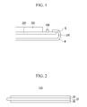
- a display device according to an exemplary embodiment of the present invention will now be described with reference to FIG. 1 .
- FIG. 1 is a view of a side surface of a display device according to an exemplary embodiment of the present invention.
- a display device includes, for example, a display substrate 200, an encapsulation substrate 300 facing the display substrate 200, and a flexible printed circuit film 100 receiving a video signal from outside the display substrate 200 and transmitting the video signal to the display substrate 200.
- the display substrate 200 may be, for example, a flexible substrate, and includes a plurality of light emitting elements forming pixels each connected to a gate line and a data line. Also, the display substrate 200 includes, for example, a driving chip 400 transmitting the driving signals to the gate lines and the data lines.
- the encapsulation substrate 300 for encapsulating the display substrate 200 may be combined to the display substrate 200 by, for example, an encapsulation material (sealant).
- an encapsulation material for example, the encapsulation substrate 300 may be formed of a glass, quartz, ceramic or plastic material but exemplary embodiments of the present invention are not limited thereto.
- the encapsulation material may include, for example, potassium oxide (K 2 O), iron oxide (Fe 2 O 3 ), antimony oxide (Sb 2 O 3 ), zinc oxide (ZnO), phosphorous pentoxide (P 2 O 5 ), vanadium oxide (V 2 O 5 ), aluminum oxide (Al 2 O 3 ), boron oxide (B 2 O 3 ), tungsten oxide (WO 3 ), tin oxide (SnO), lead oxide (PbO), and a mixture of two or more of the foregoing.
- the flexible printed circuit film 100 includes, for example, a bending region (B).
- One end of the flexible printed circuit film 100 is connected to of an upper surface of the display substrate 200 in a peripheral area (i.e. a non-pixel area) of the display substrate 200 and is bent at the bending region (B) such that a portion of the flexible printed circuit film 100 is positioned under the display substrate 200 - i.e. facing a lower surface of the display substrate 200 opposite to the upper surface - and the other end of the flexible printed circuit film 100 is connected to an external device.
- the bending region (B) of the flexible printed circuit film 100 is positioned between the portion of the flexible printed circuit film 100 connected to the display substrate 200 and a portion of the flexible printed circuit film 100 positioned under the display substrate 200 and extending parallel to the display substrate 200.
- FIG. 2 is a view of a side surface of a flexible printed circuit film according to an exemplary embodiment of the present invention
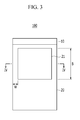
- FIG. 3 is a view of a plane surface of a flexible printed circuit film according to an exemplary embodiment of the present invention
- FIG. 4 is a cross-sectional view of the flexible printed circuit film of FIG. 3 taken along the line IV-IV.
- the flexible printed circuit film 100 includes, for example, a main body 10, a first cover layer 20 disposed on a first side of the main body 10, and a second cover layer 30 disposed on a second side of the main body 10 opposite to the first side of the main body 10.
- the first cover layer 20 and the second cover layer 30 protect the main body 10 and are attached to the main body 10 by, for example, an adhesive.
- the adhesive may be made of an acryl- or epoxy-based material.
- a length of the first cover layer and/or the second cover layer may be, for example, shorter than a length of the main body 10.
- the main body 10 includes, for example, a wire to transmit the driving signal to the driving chip 400.
- the main body 10 includes the bending region (B).
- the first cover layer 20 and the second cover layer 30 are not disposed on a region of the main body 10 corresponding to the end of the flexible printed circuit film 100 which is connected to the display substrate 200.
- the first cover layer 20 and the second cover layer 30 respectively include, for example, a first opening 21 and a second opening 31 exposing a portion of the bending region (B) of the main body 10. That is, the first cover layer 20 and the second cover layer 30 are only disposed at both lateral edges of the bending region (B) of the main body 10, as shown in Fig. 3 .
- the lateral edges of the bending region (B) extend along the long side of the main body 10 from a portion of the main body 10 connected to the display substrate 200 and a portion of the main body 10 positioned under the display substrate 200.
- the first opening 21 and the second opening 31 may extend outside of the bending region (B).
- the durability of the bending region (B) may be deteriorated such that the edges of the bending region (B) may be torn.
- the tension of the main body 10 may be increased such that a lift-off phenomenon may be generated in the display substrate 200.
- the first cover layer 20 and the second cover layer 30 are respectively disposed only at both lateral edges of the bending region (B) of the main body 10 such that the durability of the bending region (B) may be increased without increasing the tension of the main body 10.
- the widths of the first cover layer 20 and the second cover layer 30 disposed at both edges of the bending region B of the main body 10 are respectively in a range from, for example, about 0.5 mm to about 1.5 mm.
Landscapes
- Engineering & Computer Science (AREA)
- Microelectronics & Electronic Packaging (AREA)
- Physics & Mathematics (AREA)
- General Physics & Mathematics (AREA)
- Theoretical Computer Science (AREA)
- Electroluminescent Light Sources (AREA)
- Devices For Indicating Variable Information By Combining Individual Elements (AREA)
- Non-Metallic Protective Coatings For Printed Circuits (AREA)
Abstract
Description
- The present disclosure relates to a flexible printed circuit film and a display device including the same.
- Display devices include, for example, liquid crystal displays (LCD), organic light emitting diode (OLED) displays, or the like. For example, the organic light emitting diode display includes a display substrate which provides pixel areas and non-pixel areas, and an encapsulation substrate disposed to face the display substrate for encapsulation and bonded with the display substrate by a sealant such as an epoxy.
- A plurality of light emitting elements, which are connected in a matrix manner so as to configure the pixels, are formed between scan lines and data lines in the pixel area of the display substrate. A scan driver and a data driver, from which the scan lines and the data lines extend in the pixel area, process signals provided from the outside via a pad, supply the signals to the scan lines and the data lines, and are formed in the non-pixel area.
- The display device further includes, for example, a flexible printed circuit film which receives a video signal from the outside of the display substrate and respectively applies the driving signals to the gate lines and the data lines.
- The flexible printed circuit film is bent such that a portion of the flexible printed circuit film is positioned under the display substrate. When bending the flexible printed circuit film, the flexible printed circuit film may be torn at the bent portion.
- Exemplary embodiments of the present invention provide a flexible printed circuit film with increased durability of a bending region, and a display device including the same.
- A flexible printed circuit film according to an exemplary embodiment of the present invention includes a main body including a bending region, and a first cover layer disposed on a first side of the main body, and the first cover layer has a first opening exposing a portion of the bending region.
- The first cover layer may be disposed on opposing edges of the bending region on the first side of the main body.
- A width of the first cover layer disposed on the opposing edges of the bending region on the first side of the main body may be in a range from about 0.5 mm to about 1.5 mm (more preferably from about 0.7 mm to about 1.2 mm). These values result in an improved trade-off between durability of the bending region which may be fairly increased and tension of the main body which is can be prevented from being rather increased.
- A flexible printed circuit film according to an exemplary embodiment of the present invention may further include a second cover layer disposed on a second side of the main body which is opposite to the first side of the main body.
- The second cover layer may include a second opening exposing a portion of the bending region.
- The second cover layer may be disposed on opposing edges of the bending region on the second side of the main body.
- A width of the second cover layer disposed on the opposing edges of the bending region on the second side of the main body may be in a range from about 0.5 mm to about 1.5 mm (more preferably from about 0.7 mm to about 1.2 mm). These values result in an improved trade-off between durability of the bending region which may be fairly increased and tension of the main body which is can be prevented from being rather increased.
- Preferably, the main body is formed having a longish stripe-like shape. Preferably, the main body has a uniform width. Preferably, the main body has a uniform thickness. The main body has a first end and a second end. The bending region is disposed between the first end and second end.
- Preferably, the first cover layer is formed with a longish stripe-like shape except in the bending region where the first cover layer has the first opening exposing a portion of the bending region. More preferably, the width of the first cover layer outside the bending region is equal to or greater than a width of the main body. In the bending region - where first opening is located - the sum of a first width of the first cover layer extending along a first lateral edge of the bending region, a second width of the first cover layer extending along a second (opposing) lateral edge of the bending region and a width of the first opening is equal to or greater than a width of the main body.
- Preferably, the first cover layer has a uniform width. Preferably, the first cover layer has a uniform thickness outside the bending region. Preferably, the first width of the first cover layer extending along the first lateral edge of the bending region is equal to the second width of the first cover layer extending along the second (opposing) lateral edge of the bending region.
- Preferably, the first opening has a shape of an rectangle. Preferably, the first opening extends over the complete bending region along a length direction while the first opening does not extend over the complete bending region along a width direction. Preferably, exactly one opening is formed in the first cover layer
- Preferably, the second cover layer is formed with a longish stripe-like shape except in the bending region where the second cover layer has the second opening exposing a portion of the bending region. More preferably, the width of the second cover layer outside the bending region is equal to or greater than a width of the main body. In the bending region - where second opening is located - the sum of a third width of the second cover layer extending along the first lateral edge of the bending region, a fourth width of the second cover layer extending along the second (opposing) lateral edge of the bending region and a width of the second opening is equal to or greater than a width of the main body.
- Preferably, the second cover layer has a uniform width. Preferably, the second cover layer has a uniform thickness outside the bending region. Preferably, the third width is equal to the fourth width.
- Preferably, the second opening has a shape of an rectangle. Preferably, the second opening extends over the complete bending region along a length direction while the second opening does not extend over the complete bending region along a width direction Preferably, exactly one opening is formed in the second cover layer
- Preferably, the first width is equal to the third width and/or the second width is equal to the fourth width. Preferably, the second opening has a shape of an rectangle. Preferably, the second opening extends over the complete bending region.
- Preferably, the first cover layer and the second cover layer are arranged to be congruent with each other of opposite sides of the main body.
- Preferably, a first width of the first cover layer extending along the first lateral edge of the bending region is smaller than a width of the first opening. Preferably, a ratio of the first width of the first cover layer extending along the first lateral edge of the bending region and a width of the first opening ranges between 0.01 and 0.5, more preferably 0.1 and 0.5.
- Preferably, a third width of the second cover layer extending along the first lateral edge of the bending region is smaller than a width of the second opening. Preferably, a ratio of the third width of the second cover layer extending along the first lateral edge of the bending region and a width of the second opening ranges between 0.01 and 0.5, more preferably 0.1 and 0.5.
- A display device according to an exemplary embodiment of the present invention includes a display substrate, and a flexible printed circuit film according to the present invention connected to the display substrate.
- The display substrate may be a flexible substrate.
- Preferably, one end of the flexible printed circuit film is connected such to display substrate and the other end of the flexible printed circuit film is connected such to an external device that the complete bending region is bent. Preferably, a cross section of the bending region is formed as an circular arc, more preferably as a semi circle.
- Preferably, a length of the first cover layer and/or the second cover layer may be shorter than a length of the main body. Preferably, a length of the first cover layer is equal to a length of the second cover layer. Preferably, the first cover layer, the second cover layer and the main body have a congruent end section in one (lengthwise) end portion while the main body extends over the first cover layer and the second cover layer in the opposite (lengthwise) end portion.
- A flexible printed circuit film according to an exemplary embodiment of the present invention includes a main body including a bending region, and a first cover layer disposed on a first side of the main body. The first cover layer has a first opening exposing a portion of the bending region.
- In accordance with an exemplary embodiment of the present invention, a display device is provided. The display device includes a display substrate, a flexible printed circuit film connected to the display substrate, and an encapsulation substrate facing the display substrate and configured to encapsulate the display substrate.
- The flexible printed circuit film includes a main body including a bending region, in which the bending region of the flexible printed circuit film is disposed between a portion of the flexible printed circuit film connected to the display substrate and a portion of the flexible printed circuit film disposed under the display substrate and extending parallel to the display substrate.
- In addition, the flexible printed circuit film further includes a first cover layer disposed on a top surface of the main body on opposing edges of the bending region of the main body, and a second cover layer disposed on a bottom surface of the main body opposite to the top surface on opposing edges of the bending region of the main body. The first cover layer has a first opening exposing a portion of the bending region and the second cover layer has a second opening exposing a portion of the bending region. The first cover layer and the second cover layer are not disposed on a front surface of the main body. A width of the first cover layer disposed on the opposing edges of the bending region on the top surface of the main body is in a range from about 0.5 mm to about 1.5 mm and a width of the second cover layer disposed on the opposing edges of the bending region on the bottom surface of the main body is in a range from about 0.5 mm to about 1.5 mm.
- As described above, according to an exemplary embodiment of the present invention, by disposing a cover layer at both edges of the bending region of the flexible printed circuit film, an increase of the tension of the flexible printed circuit film is not generated such that tearing may be prevented in the bending region.
- Exemplary embodiments of the present invention can be understood in more detail from the following detailed description taken in conjunction with the attached drawings, in which:
-
FIG. 1 is a view of a side surface of a display device according to an exemplary embodiment of the present invention. -
FIG. 2 is a view of a side surface of a flexible printed circuit film according to an exemplary embodiment of the present invention. -
FIG. 3 is a view of a plane surface of a flexible printed circuit film according to an exemplary embodiment of the present invention. -
FIG. 4 is a cross-sectional view of the flexible printed circuit film ofFIG. 3 taken along the line IV-IV. - Exemplary embodiments of the present invention will now be described in detail with reference to the attached drawings. Exemplary embodiments of the present invention may be modified in many different forms, and should not be construed as being limited to exemplary embodiments set forth herein.
- In the drawings, the thickness of layers and regions may be exaggerated for clarity. In addition, when a layer is described to be formed on another layer or on a substrate, this means that the layer may be formed on the other layer or on the substrate, or a third layer may be interposed between the layer and the other layer or the substrate. Like numbers refer to like elements throughout the specification.
- As used herein, the singular forms, "a", "an" and "the" are intended to include the plural forms as well, unless the context clearly indicates otherwise.
- A display device according to an exemplary embodiment of the present invention will now be described with reference to
FIG. 1 . -
FIG. 1 is a view of a side surface of a display device according to an exemplary embodiment of the present invention. - Referring to
FIG. 1 , a display device according to an exemplary embodiment of the present invention includes, for example, adisplay substrate 200, anencapsulation substrate 300 facing thedisplay substrate 200, and a flexible printedcircuit film 100 receiving a video signal from outside thedisplay substrate 200 and transmitting the video signal to thedisplay substrate 200. - The
display substrate 200 may be, for example, a flexible substrate, and includes a plurality of light emitting elements forming pixels each connected to a gate line and a data line. Also, thedisplay substrate 200 includes, for example, adriving chip 400 transmitting the driving signals to the gate lines and the data lines. - The
encapsulation substrate 300 for encapsulating thedisplay substrate 200 may be combined to thedisplay substrate 200 by, for example, an encapsulation material (sealant). For example, in an embodiment, theencapsulation substrate 300 may be formed of a glass, quartz, ceramic or plastic material but exemplary embodiments of the present invention are not limited thereto. - The encapsulation material (sealant) may include, for example, potassium oxide (K2O), iron oxide (Fe2O3), antimony oxide (Sb2O3), zinc oxide (ZnO), phosphorous pentoxide (P2O5), vanadium oxide (V2O5), aluminum oxide (Al2O3), boron oxide (B2O3), tungsten oxide (WO3), tin oxide (SnO), lead oxide (PbO), and a mixture of two or more of the foregoing.
- The flexible printed
circuit film 100 includes, for example, a bending region (B). One end of the flexible printedcircuit film 100 is connected to of an upper surface of thedisplay substrate 200 in a peripheral area (i.e. a non-pixel area) of thedisplay substrate 200 and is bent at the bending region (B) such that a portion of the flexible printedcircuit film 100 is positioned under the display substrate 200 - i.e. facing a lower surface of thedisplay substrate 200 opposite to the upper surface - and the other end of the flexible printedcircuit film 100 is connected to an external device. - Here, the bending region (B) of the flexible printed
circuit film 100 is positioned between the portion of the flexible printedcircuit film 100 connected to thedisplay substrate 200 and a portion of the flexible printedcircuit film 100 positioned under thedisplay substrate 200 and extending parallel to thedisplay substrate 200. - Next, a flexible printed circuit film according to an exemplary embodiment of the present invention will be described with reference to
FIG. 2 to FIG. 4 . -
FIG. 2 is a view of a side surface of a flexible printed circuit film according to an exemplary embodiment of the present invention,FIG. 3 is a view of a plane surface of a flexible printed circuit film according to an exemplary embodiment of the present invention, andFIG. 4 is a cross-sectional view of the flexible printed circuit film ofFIG. 3 taken along the line IV-IV. - Referring to
FIG. 2 to FIG. 4 , the flexible printedcircuit film 100 according to an exemplary embodiment of the present invention includes, for example, amain body 10, afirst cover layer 20 disposed on a first side of themain body 10, and asecond cover layer 30 disposed on a second side of themain body 10 opposite to the first side of themain body 10. - The
first cover layer 20 and thesecond cover layer 30 protect themain body 10 and are attached to themain body 10 by, for example, an adhesive. For example, in an embodiment, the adhesive may be made of an acryl- or epoxy-based material. Also, a length of the first cover layer and/or the second cover layer may be, for example, shorter than a length of themain body 10. - The
main body 10 includes, for example, a wire to transmit the driving signal to thedriving chip 400. - The
main body 10 includes the bending region (B). Preferably, thefirst cover layer 20 and thesecond cover layer 30 are not disposed on a region of themain body 10 corresponding to the end of the flexible printedcircuit film 100 which is connected to thedisplay substrate 200. Thefirst cover layer 20 and thesecond cover layer 30 respectively include, for example, afirst opening 21 and asecond opening 31 exposing a portion of the bending region (B) of themain body 10. That is, thefirst cover layer 20 and thesecond cover layer 30 are only disposed at both lateral edges of the bending region (B) of themain body 10, as shown inFig. 3 . The lateral edges of the bending region (B) extend along the long side of themain body 10 from a portion of themain body 10 connected to thedisplay substrate 200 and a portion of themain body 10 positioned under thedisplay substrate 200. On the other hand, thefirst opening 21 and thesecond opening 31 may extend outside of the bending region (B). - When the
first cover layer 20 and thesecond cover layer 30 are not formed on the bending region (B) of themain body 10, the durability of the bending region (B) may be deteriorated such that the edges of the bending region (B) may be torn. On the other side, when thefirst cover layer 20 and thesecond cover layer 30 are formed on the front surface of the bending region (B) of themain body 10, the tension of themain body 10 may be increased such that a lift-off phenomenon may be generated in thedisplay substrate 200. - Accordingly, as shown in the present exemplary embodiment, the
first cover layer 20 and thesecond cover layer 30 are respectively disposed only at both lateral edges of the bending region (B) of themain body 10 such that the durability of the bending region (B) may be increased without increasing the tension of themain body 10. - The widths of the
first cover layer 20 and thesecond cover layer 30 disposed at both edges of the bending region B of themain body 10 are respectively in a range from, for example, about 0.5 mm to about 1.5 mm. - As described above, by disposing the cover layer at both edges of the bending region of the flexible printed circuit film, an increase of the tension of the flexible printed circuit film may not be generated such that tearing may be prevented in the bending region.
- Having described exemplary embodiments of the present invention, it is further noted that it is readily apparent to those of ordinary skill in the art that various modifications may be made without departing from the scope of the invention which is defined by the metes and bounds of the appended claims.
Claims (12)
- A flexible printed circuit (100) film comprising:a main body (10) including a bending region (B); anda first cover layer (20) disposed on a first side of the main body (10),wherein the first cover layer (20) has a first opening (21) exposing a portion of the bending region (B).
- The flexible printed circuit film of claim 1, wherein the first cover (20) layer is disposed on opposing lateral edges of the bending region (B) on the first side of the main body (10).
- The flexible printed circuit film of claim 2, wherein a width of the first cover layer (20) disposed on the opposing lateral edges of the bending region (B) on the first side of the main body (10) is in a range from 0.5 mm to 1.5 mm.
- The flexible printed circuit film of one of the preceding claims, further comprising a second cover layer (30) disposed on a second side of the main body (10) which is opposite to the first side of the main body (10).
- The flexible printed circuit film of claim 4, wherein the second cover layer (30) includes a second opening (31) exposing a portion of the bending region (B).
- The flexible printed circuit film of claim 5, wherein the second cover layer (30) is disposed on opposing lateral edges of the bending region (B) on the second side of the main body (10).
- The flexible printed circuit film of claim 6, wherein a width of the second cover layer (30) disposed on the opposing lateral edges of the bending region (B) on the second side of the main body (10) is in a range from 0.5 mm to 1.5 mm.
- A display device comprising:a display substrate (200); anda flexible printed circuit film (100) according to any of the preceding claims, wherein a first end portion of the flexible printed circuit film (100) is connected to an upper surface of the display substrate (200).
- The display device of claim 8, wherein the bending region (B) of the flexible printed circuit film (100) is disposed between the first end portion of the flexible printed circuit film (100) and a portion of the flexible printed circuit film (100) disposed under the display substrate (200) and extending parallel to a lower surface of the display substrate (200) opposite to the upper surface of the display substrate (200).
- The display device of one of claim 9, wherein a second end portion of the flexible printed circuit film (100) opposite to the first end portion is adapted to be connected to an external device for supplying a video signal.
- The display device of one of claims 8 to 10, further comprising:an encapsulation substrate (300) located on the upper surface of the display substrate (200); anda driving chip (400) located on the upper surface of the display substrate (200) and electrically connected to the flexible printed circuit film (100).
- The display device of one of claims 8 to 11, wherein the display substrate (200) is a flexible substrate.
Applications Claiming Priority (1)
| Application Number | Priority Date | Filing Date | Title |
|---|---|---|---|
| KR1020130084786A KR20150010161A (en) | 2013-07-18 | 2013-07-18 | Flexible printed circuit film and display device including the same |
Publications (1)
| Publication Number | Publication Date |
|---|---|
| EP2827686A1 true EP2827686A1 (en) | 2015-01-21 |
Family
ID=50442342
Family Applications (1)
| Application Number | Title | Priority Date | Filing Date |
|---|---|---|---|
| EP14161398.4A Withdrawn EP2827686A1 (en) | 2013-07-18 | 2014-03-25 | Flexible printed circuit film and display device including the same |
Country Status (6)
| Country | Link |
|---|---|
| US (1) | US20150022953A1 (en) |
| EP (1) | EP2827686A1 (en) |
| JP (1) | JP2015023278A (en) |
| KR (1) | KR20150010161A (en) |
| CN (1) | CN104302093A (en) |
| TW (1) | TW201508382A (en) |
Families Citing this family (4)
| Publication number | Priority date | Publication date | Assignee | Title |
|---|---|---|---|---|
| US9490312B2 (en) * | 2014-12-22 | 2016-11-08 | Lg Display Co., Ltd. | Organic light emitting diode display device with flexible printed circuit film |
| KR102415324B1 (en) * | 2015-05-04 | 2022-06-30 | 삼성디스플레이 주식회사 | Touch panel and method for manufacturing the same |
| CN104991369B (en) * | 2015-08-06 | 2019-02-05 | 京东方科技集团股份有限公司 | Display module and display device |
| CN204884440U (en) * | 2015-08-27 | 2015-12-16 | 京东方科技集团股份有限公司 | Flexible display panel and flexible display device |
Citations (8)
| Publication number | Priority date | Publication date | Assignee | Title |
|---|---|---|---|---|
| US4756940A (en) * | 1986-03-25 | 1988-07-12 | Tektronix, Inc. | Flexible circuit strain relief |
| US20070159801A1 (en) * | 2005-12-21 | 2007-07-12 | Motorola, Inc. | Insert molded flexible circuit with stiffener and flip housing assembly and method of manufacture |
| US20070177093A1 (en) * | 2006-01-27 | 2007-08-02 | Eiji Oohira | Display device |
| EP1830336A1 (en) * | 2005-02-22 | 2007-09-05 | FUJIFILM Corporation | Flexible substrate supprerssed from being plastically deformed, and flexible image display device |
| US20090213314A1 (en) * | 2008-02-25 | 2009-08-27 | Hitachi Displays, Ltd. | Liquid crystal display device and manufacturing method therefor |
| US20100084169A1 (en) * | 2007-02-20 | 2010-04-08 | Shigehiro Nakamura | Flexible multilayer wiring board |
| US20120212445A1 (en) * | 2011-02-23 | 2012-08-23 | Nokia Corporation | Display With Rear Side Capacitive Touch Sensing |
| US20130133930A1 (en) * | 2011-11-28 | 2013-05-30 | Fujikura Ltd. | Printed wiring board |
Family Cites Families (5)
| Publication number | Priority date | Publication date | Assignee | Title |
|---|---|---|---|---|
| CN201174842Y (en) * | 2008-04-02 | 2008-12-31 | 胜华科技股份有限公司 | electronic device |
| US20100253902A1 (en) * | 2009-04-07 | 2010-10-07 | Semiconductor Energy Laboratory Co., Ltd. | Liquid crystal display device and manufacturing method thereof |
| CN101909398B (en) * | 2009-06-04 | 2012-03-21 | 纬创资通股份有限公司 | Electronic device and its flexible circuit board |
| CN201550352U (en) * | 2009-07-27 | 2010-08-11 | 天马微电子股份有限公司 | Flexible PCB and LCM employing same |
| CN102438394A (en) * | 2011-09-28 | 2012-05-02 | 四川虹欧显示器件有限公司 | Flexible circuit board |
-
2013
- 2013-07-18 KR KR1020130084786A patent/KR20150010161A/en not_active Withdrawn
-
2014
- 2014-02-05 US US14/173,140 patent/US20150022953A1/en not_active Abandoned
- 2014-03-25 EP EP14161398.4A patent/EP2827686A1/en not_active Withdrawn
- 2014-04-15 CN CN201410150812.4A patent/CN104302093A/en active Pending
- 2014-04-16 TW TW103113798A patent/TW201508382A/en unknown
- 2014-06-02 JP JP2014114148A patent/JP2015023278A/en active Pending
Patent Citations (8)
| Publication number | Priority date | Publication date | Assignee | Title |
|---|---|---|---|---|
| US4756940A (en) * | 1986-03-25 | 1988-07-12 | Tektronix, Inc. | Flexible circuit strain relief |
| EP1830336A1 (en) * | 2005-02-22 | 2007-09-05 | FUJIFILM Corporation | Flexible substrate supprerssed from being plastically deformed, and flexible image display device |
| US20070159801A1 (en) * | 2005-12-21 | 2007-07-12 | Motorola, Inc. | Insert molded flexible circuit with stiffener and flip housing assembly and method of manufacture |
| US20070177093A1 (en) * | 2006-01-27 | 2007-08-02 | Eiji Oohira | Display device |
| US20100084169A1 (en) * | 2007-02-20 | 2010-04-08 | Shigehiro Nakamura | Flexible multilayer wiring board |
| US20090213314A1 (en) * | 2008-02-25 | 2009-08-27 | Hitachi Displays, Ltd. | Liquid crystal display device and manufacturing method therefor |
| US20120212445A1 (en) * | 2011-02-23 | 2012-08-23 | Nokia Corporation | Display With Rear Side Capacitive Touch Sensing |
| US20130133930A1 (en) * | 2011-11-28 | 2013-05-30 | Fujikura Ltd. | Printed wiring board |
Also Published As
| Publication number | Publication date |
|---|---|
| TW201508382A (en) | 2015-03-01 |
| KR20150010161A (en) | 2015-01-28 |
| JP2015023278A (en) | 2015-02-02 |
| CN104302093A (en) | 2015-01-21 |
| US20150022953A1 (en) | 2015-01-22 |
Similar Documents
| Publication | Publication Date | Title |
|---|---|---|
| EP3608964B1 (en) | Stretchable display device | |
| US11049926B2 (en) | Stretchable display device | |
| US10409096B2 (en) | Display device | |
| KR102706521B1 (en) | Stretchable display device | |
| US10714703B2 (en) | Organic light emitting diode display device | |
| CN111199995B (en) | Telescopic display device | |
| US9865838B2 (en) | Display device having a bent portion | |
| US9609758B2 (en) | Display device and method of manufacturing the same | |
| KR20210012391A (en) | Stretchable display device | |
| KR20200039973A (en) | Stretchable display device and manufacturing method the same | |
| KR102706332B1 (en) | Touch panel and stretchable display device comprising the same | |
| KR20160063483A (en) | Display device | |
| EP2827686A1 (en) | Flexible printed circuit film and display device including the same | |
| KR20210053559A (en) | Stretchable display device | |
| JP6553382B2 (en) | Display device | |
| KR102794900B1 (en) | Stretchable display device | |
| CN116322171A (en) | display screen | |
| US20240081112A1 (en) | Display device including elastic protrusions on pad area of substrate | |
| KR102569924B1 (en) | Organic light emitting display panel and fabricating method of the same | |
| US20240222341A1 (en) | Display device | |
| KR102957074B1 (en) | Stretchable display | |
| US12360627B2 (en) | Display device having discharge patterns in a pad area to discharge static electricity introduced into a driver | |
| KR20210058333A (en) | Display device | |
| KR102955963B1 (en) | Display device | |
| KR20220003774A (en) | Stretchable display |
Legal Events
| Date | Code | Title | Description |
|---|---|---|---|
| 17P | Request for examination filed |
Effective date: 20140325 |
|
| AK | Designated contracting states |
Kind code of ref document: A1 Designated state(s): AL AT BE BG CH CY CZ DE DK EE ES FI FR GB GR HR HU IE IS IT LI LT LU LV MC MK MT NL NO PL PT RO RS SE SI SK SM TR |
|
| AX | Request for extension of the european patent |
Extension state: BA ME |
|
| PUAI | Public reference made under article 153(3) epc to a published international application that has entered the european phase |
Free format text: ORIGINAL CODE: 0009012 |
|
| R17P | Request for examination filed (corrected) |
Effective date: 20150713 |
|
| RBV | Designated contracting states (corrected) |
Designated state(s): AL AT BE BG CH CY CZ DE DK EE ES FI FR GB GR HR HU IE IS IT LI LT LU LV MC MK MT NL NO PL PT RO RS SE SI SK SM TR |
|
| RAP1 | Party data changed (applicant data changed or rights of an application transferred) |
Owner name: SAMSUNG DISPLAY CO., LTD. |
|
| 17Q | First examination report despatched |
Effective date: 20160714 |
|
| STAA | Information on the status of an ep patent application or granted ep patent |
Free format text: STATUS: EXAMINATION IS IN PROGRESS |
|
| STAA | Information on the status of an ep patent application or granted ep patent |
Free format text: STATUS: THE APPLICATION IS DEEMED TO BE WITHDRAWN |
|
| 18D | Application deemed to be withdrawn |
Effective date: 20161125 |