EP2827482A2 - Power control device and image forming apparatus inlcuding the same - Google Patents
Power control device and image forming apparatus inlcuding the same Download PDFInfo
- Publication number
- EP2827482A2 EP2827482A2 EP14168711.1A EP14168711A EP2827482A2 EP 2827482 A2 EP2827482 A2 EP 2827482A2 EP 14168711 A EP14168711 A EP 14168711A EP 2827482 A2 EP2827482 A2 EP 2827482A2
- Authority
- EP
- European Patent Office
- Prior art keywords
- power
- resistor
- transistor
- control device
- switch
- Prior art date
- Legal status (The legal status is an assumption and is not a legal conclusion. Google has not performed a legal analysis and makes no representation as to the accuracy of the status listed.)
- Granted
Links
Images




Classifications
-
- G—PHYSICS
- G03—PHOTOGRAPHY; CINEMATOGRAPHY; ANALOGOUS TECHNIQUES USING WAVES OTHER THAN OPTICAL WAVES; ELECTROGRAPHY; HOLOGRAPHY
- G03G—ELECTROGRAPHY; ELECTROPHOTOGRAPHY; MAGNETOGRAPHY
- G03G21/00—Arrangements not provided for by groups G03G13/00 - G03G19/00, e.g. cleaning, elimination of residual charge
-
- H—ELECTRICITY
- H02—GENERATION; CONVERSION OR DISTRIBUTION OF ELECTRIC POWER
- H02M—APPARATUS FOR CONVERSION BETWEEN AC AND AC, BETWEEN AC AND DC, OR BETWEEN DC AND DC, AND FOR USE WITH MAINS OR SIMILAR POWER SUPPLY SYSTEMS; CONVERSION OF DC OR AC INPUT POWER INTO SURGE OUTPUT POWER; CONTROL OR REGULATION THEREOF
- H02M1/00—Details of apparatus for conversion
- H02M1/32—Means for protecting converters other than automatic disconnection
-
- H—ELECTRICITY
- H02—GENERATION; CONVERSION OR DISTRIBUTION OF ELECTRIC POWER
- H02J—ELECTRIC POWER NETWORKS; CIRCUIT ARRANGEMENTS OR SYSTEMS FOR SUPPLYING OR DISTRIBUTING ELECTRIC POWER; SYSTEMS FOR STORING ELECTRIC ENERGY
- H02J13/00—Circuit arrangements for providing remote monitoring or remote control of equipment in a power distribution network
-
- H—ELECTRICITY
- H02—GENERATION; CONVERSION OR DISTRIBUTION OF ELECTRIC POWER
- H02M—APPARATUS FOR CONVERSION BETWEEN AC AND AC, BETWEEN AC AND DC, OR BETWEEN DC AND DC, AND FOR USE WITH MAINS OR SIMILAR POWER SUPPLY SYSTEMS; CONVERSION OF DC OR AC INPUT POWER INTO SURGE OUTPUT POWER; CONTROL OR REGULATION THEREOF
- H02M1/00—Details of apparatus for conversion
- H02M1/12—Arrangements for reducing harmonics from AC input or output
-
- H—ELECTRICITY
- H02—GENERATION; CONVERSION OR DISTRIBUTION OF ELECTRIC POWER
- H02M—APPARATUS FOR CONVERSION BETWEEN AC AND AC, BETWEEN AC AND DC, OR BETWEEN DC AND DC, AND FOR USE WITH MAINS OR SIMILAR POWER SUPPLY SYSTEMS; CONVERSION OF DC OR AC INPUT POWER INTO SURGE OUTPUT POWER; CONTROL OR REGULATION THEREOF
- H02M1/00—Details of apparatus for conversion
- H02M1/36—Means for starting or stopping converters
-
- H—ELECTRICITY
- H02—GENERATION; CONVERSION OR DISTRIBUTION OF ELECTRIC POWER
- H02M—APPARATUS FOR CONVERSION BETWEEN AC AND AC, BETWEEN AC AND DC, OR BETWEEN DC AND DC, AND FOR USE WITH MAINS OR SIMILAR POWER SUPPLY SYSTEMS; CONVERSION OF DC OR AC INPUT POWER INTO SURGE OUTPUT POWER; CONTROL OR REGULATION THEREOF
- H02M7/00—Conversion of AC power input into DC power output; Conversion of DC power input into AC power output
- H02M7/02—Conversion of AC power input into DC power output without possibility of reversal
- H02M7/04—Conversion of AC power input into DC power output without possibility of reversal by static converters
- H02M7/12—Conversion of AC power input into DC power output without possibility of reversal by static converters using discharge tubes with control electrode or semiconductor devices with control electrode
-
- H—ELECTRICITY
- H02—GENERATION; CONVERSION OR DISTRIBUTION OF ELECTRIC POWER
- H02H—EMERGENCY PROTECTIVE CIRCUIT ARRANGEMENTS
- H02H7/00—Emergency protective circuit arrangements specially adapted for specific types of electric machines or apparatus or for sectionalised protection of cable or line systems, and effecting automatic switching in the event of an undesired change from normal working conditions
- H02H7/10—Emergency protective circuit arrangements specially adapted for specific types of electric machines or apparatus or for sectionalised protection of cable or line systems, and effecting automatic switching in the event of an undesired change from normal working conditions for converters; for rectifiers
- H02H7/12—Emergency protective circuit arrangements specially adapted for specific types of electric machines or apparatus or for sectionalised protection of cable or line systems, and effecting automatic switching in the event of an undesired change from normal working conditions for converters; for rectifiers for static converters or rectifiers
- H02H7/125—Emergency protective circuit arrangements specially adapted for specific types of electric machines or apparatus or for sectionalised protection of cable or line systems, and effecting automatic switching in the event of an undesired change from normal working conditions for converters; for rectifiers for static converters or rectifiers for rectifiers
- H02H7/127—Emergency protective circuit arrangements specially adapted for specific types of electric machines or apparatus or for sectionalised protection of cable or line systems, and effecting automatic switching in the event of an undesired change from normal working conditions for converters; for rectifiers for static converters or rectifiers for rectifiers having auxiliary control electrode to which blocking control voltages or currents are applied in case of emergency
-
- H—ELECTRICITY
- H02—GENERATION; CONVERSION OR DISTRIBUTION OF ELECTRIC POWER
- H02M—APPARATUS FOR CONVERSION BETWEEN AC AND AC, BETWEEN AC AND DC, OR BETWEEN DC AND DC, AND FOR USE WITH MAINS OR SIMILAR POWER SUPPLY SYSTEMS; CONVERSION OF DC OR AC INPUT POWER INTO SURGE OUTPUT POWER; CONTROL OR REGULATION THEREOF
- H02M1/00—Details of apparatus for conversion
- H02M1/32—Means for protecting converters other than automatic disconnection
- H02M1/322—Means for rapidly discharging a capacitor of the converter for protecting electrical components or for preventing electrical shock
Definitions
- Embodiments relate to a power control device and an image forming apparatus including the same. More specifically, embodiments relate to a power control device configured to reduce standby power consumption, and an image forming apparatus including the same.
- an electromagnetic interference (EMI) filter for removing noise is included in an input of a power supply (e.g. a switch-mode power supply), and if electrical charges of an X-capacitor included in the EMI filter flow to a metal terminal of a plug during a plug-off state, a safety problem may occur. Accordingly, in order to solve the problem, a discharge resistor configured to discharge charges filled in the X-capacitor may be used. However, there is power consumption in a plug-on state due to the discharge resistor, which is against the effort for reducing the standby power consumption of electrical appliances. Therefore, measures to solve the problem are needed.
- a power supply e.g. a switch-mode power supply
- a power control device which meets the need for low power consumption by minimizing standby power consumption in a plug-on state of an electronic apparatus, and meets the safety requirements by increasing a discharging rate of an X-cap or an E-cap in a plug-off state.
- a power control device which includes a first capacitor charged by AC power during input of the AC power, a rectifier converting the AC power to DC power, a second capacitor formed at an output of the rectifier, and a discharge circuit including at least one discharge resistor, and a first switch and a second switch configured to be alternately turned on/off in response to supply and interruption of the AC power.
- the discharge circuit discharges at least one of the first and second capacitors via the at least one discharge resistor, in response to turn-off of the first switch and turn-on of the second switch.
- the first capacitor may be electrically connected between input lines through which the AC power is input.
- the rectifier may be connected to the input line of the AC power.
- the first switch may be a detection circuit including a photo-coupler configured to be electrically connected between the input lines of the AC power, and turned on in response to input of the AC power and turned off in response to interruption of the AC power.
- the second capacitor may be disposed at an output of the rectifier.
- the second switch may be a discharge circuit including at least one discharge resistor and at least one first transistor which are connected in series to the output of the rectifier.
- the first switch may further include an RC series circuit electrically connected in series to the photo-coupler between the input lines of the AC power.
- the RC series circuit may include a resistor and a capacitor which are connected in series to an end of the photo-coupler, and another resistor and another capacitor which are connected in series to the other end of the photo-coupler.
- the RC series circuit may include a resistor and a capacitor which are connected in series to an end of the photo-coupler.
- the RC series circuit may include a resistor connected in series to an end of the photo-coupler, and a capacitor connected in series to the other end of the photo-coupler.
- the photo-coupler may include a light emitting device connected to the RC series circuit, and a light receiving device configured to be turned on in response to emission of the light emitting device.
- the light emitting device of the first switch may be a bidirectional light emitting diode.
- the light receiving device of the first switch may be an NPN-type photo transistor, and an emitter and a collector of the photo transistor may be electrically connected to the second switch.
- the at least one first transistor of the second switch may be a PNP-type bipolar transistor.
- An emitter of the first transistor may be connected to the discharge resistor, and a collector of the first transistor may be connected to a ground.
- the second switch may further include a detection resistor connected between a collector of the photo-transistor and the output of the rectifier.
- the second switch may have a resistivity of the detection resistor relatively greater than a resistivity of the discharge resistor.
- the second switch may include an RC parallel circuit connected between a base and a collector of the at least one first transistor.
- the second switch may further include a second transistor configured to turn on the first transistor by being turned on in response to turn-off of the photo-coupler.
- the second transistor of the second switch may be an NPN-type bipolar transistor.
- a collector of the second transistor may be connected to a base of the first transistor, and an emitter of the second transistor may be grounded.
- an image forming apparatus which includes a power control device includes a first capacitor charged by AC power during input of the AC power, a rectifier transforming the AC power to DC power, a second capacitor disposed at an output of the rectifier, and a discharge circuit including at least one discharge resistor, and a first switch and a second switch configured to be alternately turned on/off in response to supply and interruption of the AC power.
- the discharge circuit discharges at least one of the first and second capacitors via the at least one discharge resistor, in response to turn-off of the first switch and turn-on of the second switch.
- the first capacitor may be electrically connected between input lines through which the AC power is input.
- the rectifier may be connected to the input line of the AC power.
- the first switch may be a detection circuit including a photo-coupler configured to be electrically connected between the input lines of the AC power, and turned on in response to input of the AC power and turned off in response to interruption of the AC power.
- the second capacitor may be disposed at an output of the rectifier.
- the second switch may be a discharge circuit including at least one discharge resistor and at least one first transistor which are connected in series to the output of the rectifier.
- a power control device including an electromagnetic interference (EMI) filter including a first capacitor, which is charged by AC power and which removes noise; a rectifier which converts the AC power to DC power; a second capacitor which is formed between an output of the rectifier and a transformer in order to smooth DC power during interruption of AC power; and a discharge circuit includes at least one discharge resistor, and a first switch and a second switch configured to be alternately turned on/off in response to supply and interruption of the AC power, and which discharges at least one of the first and second capacitors via the at least one discharge resistor, in response to turn-off of the first switch and turn-on of the second switch.
- EMI electromagnetic interference
- FIG. 1 is a diagram showing a laser printer as an image forming apparatus in accordance with an embodiment.
- the image forming apparatus 102 includes a power cable 104 configured to receive power, and a plug 106 disposed at an end of the power cable 104. By inserting the plug 106 into a socket 108 of an outlet or multi-tab, normal AC power supplied from an external power source may be supplied to the image forming apparatus 102.
- the image forming apparatus 102 may perform a work related to image processing by receiving power through the plug 106 inserted into the socket 108, and the power cable 104.
- plug-on represents that the plug 106 is inserted into the socket 108
- plug-off represents that the plug 106 inserted in the socket 108 is separated from the socket 108.
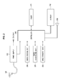
- FIG. 2 is a diagram showing a control system of the image forming apparatus illustrated in FIG. 1 .
- a controller 240 that controls overall operations of the image forming apparatus 102 is electrically connected to a paper feeding unit 230 and a paper discharging unit 220, an image transfer unit 250, a fuser 270, a display 206, and a speaker 208 in order to communicate.
- a power supply 202 for example, a switching mode power supply (SMPS), generates 5V and 24V of system DC power through AC-DC conversion, to be supplied to the controller 240, the image transfer unit 250, and other parts.
- SMPS switching mode power supply
- the 5V of DC power is supplied to a microprocessor such as a controller 240, a circuit device, etc., and the 24V of DC power is supplied to the fuser 270, etc.
- the 5V and 24V of system DC power output from the power supply 202 may be selectively supplied to other components of the image forming apparatus 102.
- the power supply 202 may supply normal power to a part that needs the power, for example, a fuser heater of the fuser 270.
- the paper feeding unit 230 supplies a printing medium (paper) loaded in a paper feeding cassette to the image transfer unit 250.
- the image transfer unit 250 forms a predetermined image according to image signals, and then transfers the image on an upper surface of the printing medium.
- the fuser 270 semi-permanently settles the image transferred on the printing medium.
- the paper discharging unit 220 discharges the printing medium on which the image is settled in the fuser 270.
- the controller 240 controls overall operations of the image forming apparatus 102, and is electrically connected to a plurality of sensors which detect the status of each part of the image forming apparatus 102 in order to communicate therewith.
- the display 206 displays an announcement message, etc. to notify a user of driving information or status information of the image forming apparatus 102.
- the speaker 208 outputs an announcement voice or alarm that occurs during operation of the image forming apparatus 102.
- FIG. 3 is a diagram showing an example of the power supply 202 described in FIG. 2 in accordance with an embodiment.
- the power supply 202 shown in FIG. 3 includes an electromagnetic interference (EMI) filter 304, a detection circuit 310 which is a first switch of a discharge circuit unit 302, a rectifier 306, a discharge circuit 312 which is a second switch of the discharge circuit unit 302, and a transformer 308.
- the EMI filter 304 is configured to remove various noise included in the power cable 104 to which normal power (AC or DC) is supplied, and is a line filter including a coil and capacitor.
- the rectifier 306 converts AC power to DC power, or AC power to another AC power having a different phase.
- the transformer 308 lowers a voltage of the DC power rectified in the rectifier 306 to generate a desired level of DC voltage.
- the discharge circuit unit 302 includes a detection circuit 310 and a discharge circuit 312, which are electrically connected to a respective front end and back end of the rectifier 306. In addition, the detection circuit 310 and the discharge circuit 312 of the discharge circuit unit 302 are electrically connected to each other, too.
- An E-capacitor (E-cap) is formed between the discharge circuit 312 of the discharge circuit unit 302 and the transformer 308. The E-cap responds to a temporary interruption of electric power and smoothes DC power flowing into a rectifying diode of the rectifier 306. A large capacitor is used as the E-cap.
- the E-cap is discharged by the discharge circuit unit 302.
- the discharge circuit unit 302 controls charges filled in the E-cap to be rapidly discharged via a discharge resistor Rdis.
- FIG. 4 is a diagram showing a power control device in accordance with an embodiment.
- the detection circuit 310 of the discharge circuit unit 302 formed at the front end of the rectifier 306 is disposed between live and neutral lines, which are AC power supply lines, and the discharge circuit 312 of the discharge circuit unit 302 formed at the back end of the rectifier 306 is disposed between the output lines of the rectifier 306.
- the detection circuit 310 is formed in such a way that a resistor R1, a capacitor C1, a photo-coupler 402, a capacitor C2, and a resistor R2 are connected in series.
- the resistor R1, the capacitor C1, the capacitor C2, and the resistor R2 configure an RC series circuit.
- the photo-coupler 402 is configured of a light emitting diode D1 which is a light emitting device, and a transistor Q1 which is a light receiving device.
- the light emitting diode D1 is a bidirectional device which responds to each of (+) polarity and (-) polarity of AC power, and (+) polarity and (-) polarity of a discharging current of an X-capacitor (X-cap).
- X-cap X-capacitor
- a collector and an emitter of the transistor Q1 are connected to the back end of the rectifier 306 respectively via a resistor R3 and resistor R5 of the discharge circuit 312. That is, the resistor R3, the transistor Q1, and the resistor R5 are connected in series to the back end of the rectifier 306.
- a discharge resistor Rdis and transistor Q2 are connected in series to the back end of the rectifier 306.
- a base of the transistor Q2 is connected between the emitter of the transistor Q1 and the resistor R5.
- a capacitor C3 is connected parallel to the resistor R5 between the base of the transistor Q2 and a ground.
- the transistor Q2 since a base voltage of the transistor Q2 becomes a high level due to a smoothing operation of the resistor R5 and capacitor C3, the transistor Q2 may be maintained in an off state without being turned on. Since the transistor Q2 is maintained in the off state, discharging of the E-cap through the resistor Rdis may not take place.
- the resistor R3 since the resistor R3 has a much greater resistance than the resistor Rdis, the amount of current flowing through the transistor Q1 which is turned on while supplying AC power, that is, the amount of current in a standby mode, is very limited. Accordingly, since the amount of a detection current flowing through the resistor R3 while supplying AC power is very small, power consumption in the standby mode can be reduced as that much.
- the X-cap which has been blocked by the rectifier 306 starts discharging, and DC power instead of AC power is supplied to the detection circuit 310.
- the capacitors C1, C2, and C3 are switched to an electrically open state, and a DC current flow due to the discharge of the X-cap is blocked.
- the transistor Q1 is turned off, and a base current of the transistor Q2 flows in a direction into the base of the transistor Q2.
- the transistor Q2 is turned on, and thereby a charge current in the X-cap and E-cap may be discharged through the resistor Rdis from when the electrical potential of the X-cap becomes higher than the electrical potential of the E-cap.
- the resistor Rdis for discharge has a relatively very small resistance compared to the resistor R3 for current detection, the resistor Rdis can discharge the charge current in the E-cap at a very fast rate.
- the power control device in accordance with an embodiment meets the need for low power consumption since while AC power is input in a plug-on state, a very small amount of current flows through the resistor R3 having a relatively very large resistance. Further, the power control device in accordance with an embodiment also meets the safety requirements since, in a plug-off state, the X-cap or the E-cap is discharged at a very fast rate through the resistor Rdis having a relatively very small resistance.
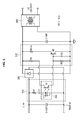
- FIG. 5 is a diagram showing a power control device in accordance with an embodiment.
- the power control device in accordance with an embodiment includes an RC series circuit configuring a detection circuit 310 of a discharge circuit unit 302, wherein the RC series circuit is configured of a single resistor R1 and a single capacitor C1.
- a detection circuit is configured of a smaller number of devices than when it consists of two resistors R1 and R2, and two capacitors C1 and C2 in the first embodiment shown in FIG. 4 , resulting in saving of components as that much.
- the detection circuit 310 of the discharge circuit unit 302 formed at a front end of a rectifier 306 is disposed between live and neutral lines, which are AC power supply lines, and a discharge circuit 312 of the discharge circuit unit 302 formed at a back end of the rectifier 306 is disposed between the output lines of the rectifier 306.
- the detection circuit 310 is formed in such a way that the resistor R1, the capacitor C1, and a photo-coupler 402 are connected in series.
- the resistor R1 and the capacitor C1 configure an RC series circuit.
- the photo-coupler 402 is configured of a light emitting diode D1 which is a light emitting device, and a transistor Q1 which is a light receiving device.
- the light emitting diode D1 is a bidirectional device which responds to each of (+) polarity and (-) polarity of AC power, and (+) polarity and (-) polarity of a discharging current of an X-cap.
- the transistor Q1 When the light emitting diode D1 is turned on to emit light, the transistor Q1 may be turned on by the emission of the light emitting diode D1.
- a collector and an emitter of the transistor Q1 are connected to the back end of the rectifier 306 respectively via a resistor R3 and a resistor R5 of the discharge circuit 312. That is, the resistor R3, the transistor Q1, and the resistor R5 are connected in series to the back end of the rectifier 306.
- a resistor Rdis and transistor Q2 for discharge are connected in series to the back end of the rectifier 306.
- a base of the transistor Q2 is connected between the emitter of the transistor Q1 and the resistor R5.
- a capacitor C3 is connected parallel to the resistor R5 between the base of the transistor Q2 and a ground.
- the transistor Q2 since a base voltage of the transistor Q2 becomes a high level due to a smoothing operation of the resistor R5 and capacitor C3, the transistor Q2 may be maintained in an off state without being turned on. Since the transistor Q2 is maintained in the off state, discharging of the E-cap through the resistor Rdis may not take place.
- the resistor R3 since the resistor R3 has a much greater resistance than the resistor Rdis, the amount of current flowing through the transistor Q1 which is turned on while supplying AC power, that is, the amount of current in a standby mode, is very limited. Accordingly, since the amount of a detection current flowing through the resistor R3 while supplying AC power is very small, power consumption in the standby mode can be reduced as that much.
- the X-cap which has been blocked by the rectifier 306 starts discharging, and DC power instead of AC power is supplied to the detection circuit 310.
- the capacitors C1 and C3 are switched to an electrically open state, and a DC current flow due to the discharge of the X-cap is blocked.
- the transistor Q1 is turned off, and a base current of the transistor Q2 flows in a direction into the base of the transistor Q2.
- the transistor Q2 is turned on, and thereby a charge current in the X-cap and E-cap may be discharged through the resistor Rdis from when the electrical potential of the X-cap becomes higher than the electrical potential of the E-cap.
- the resistor Rdis for discharge has a relatively very small resistance compared to the resistor R3 for current detection, the resistor Rdis can discharge the charge current in the E-cap at a very fast rate.
- the power control device in accordance with an embodiment meets the need for low power consumption since while AC power is input in a plug-on state, a very small amount of current flows through the resistor R3 having a relatively very large resistance. Further, the power control device in accordance with an embodiment also meets the safety requirements since, in a plug-off state, the X-cap or the E-cap is discharged at a very fast rate through the resistor Rdis having a relatively very small resistance.
- FIG. 6 is a diagram showing a power control device in accordance with an embodiment.
- the power control device in accordance with an embodiment includes an RC series circuit configuring a detection circuit 310 of a discharge circuit unit 302, wherein the RC series circuit is configured of a single resistor R1 and a single capacitor C1.
- a detection circuit is configured of a smaller number of devices than when it consists of two resistors R1 and R2, and two capacitors C1 and C2 in the first embodiment shown in FIG. 4 , resulting in saving of components as that much.
- the detection circuit 310 of the discharge circuit unit 302 formed at a front end of a rectifier 306 is disposed between live and neutral lines, which are AC power supply lines, and a discharge circuit 312 of the discharge circuit unit 302 formed at a back end of the rectifier 306 is disposed between the output lines of the rectifier 306.
- the detection circuit 310 is formed in such a way that the resistor R1, a photo-coupler 402, and the capacitor C1 are connected in series.
- the resistor R1 and the capacitor C1 configure an RC series circuit.
- the photo-coupler 402 is configured of a light emitting diode D1 which is a light emitting device, and a transistor Q1 which is a light receiving device.
- the light emitting diode D1 is a bidirectional device which responds to each of (+) polarity and (-) polarity of AC power, and (+) polarity and (-) polarity of a discharging current of an X-cap.
- the transistor Q1 When the light emitting diode D1 is turned on to emit light, the transistor Q1 may be turned on by the emission of the light emitting diode D1.
- a collector and an emitter of the transistor Q1 are connected to the back end of the rectifier 306 respectively via a resistor R3 and a resistor R5 of the discharge circuit 312. That is, the resistor R3, the transistor Q1, and the resistor R5 are connected in series to the back end of the rectifier 306.
- a resistor Rdis and transistor Q2 for discharge are connected in series to the back end of the rectifier 306.
- a base of the transistor Q2 is connected between the emitter of the transistor Q1 and the resistor R5.
- a capacitor C3 is connected parallel to the resistor R5 between the base of the transistor Q2 and a ground.
- the transistor Q2 since a base voltage of the transistor Q2 becomes a high level due to a smoothing operation of the resistor R5 and capacitor C3, the transistor Q2 may be maintained in an off state without being turned on. Since the transistor Q2 is maintained in the off state, discharging of the E-cap through the resistor Rdis may not take place.
- the resistor R3 since the resistor R3 has a much greater resistance than the resistor Rdis, the amount of current flowing through the transistor Q1 which is turned on while supplying AC power, that is, the amount of current in a standby mode, is very limited. Accordingly, since the amount of a detection current flowing through the resistor R3 while supplying AC power is very small, power consumption in the standby mode can be reduced as that much.
- the X-cap which has been blocked by the rectifier 306 starts discharging, and DC power instead of AC power is supplied to the detection circuit 310.
- the capacitors C1 and C3 are switched to an electrically open state, and a DC current flow due to the discharge of the X-cap is blocked.
- the transistor Q1 is turned off, and a base current of the transistor Q2 flows in a direction into the base of the transistor Q2.
- the transistor Q2 is turned on, and thereby a charge current in the X-cap and E-cap may be discharged through the resistor Rdis from when the electrical potential of the X-cap becomes higher than the electrical potential of the E-cap.
- the resistor Rdis for discharge has a relatively very small resistance compared to the resistor R3 for current detection, the resistor Rdis can discharge the charge current in the E-cap at a very fast rate.
- the power control device in accordance with an embodiment meets the need for low power consumption since while AC power is input in a plug-on state, a very small amount of current flows through the resistor R3 having a relatively very large resistance. Further, the power control device in accordance with an embodiment also meets the safety requirements since, in a plug-off state, the X-cap or the E-cap is discharged at a very fast rate through the resistor Rdis having a relatively very small resistance.
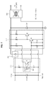
- FIG. 7 is a diagram showing a power control device in accordance with an embodiment. As shown in FIG. 7 , in the power control device in accordance with an embodiment, a degree of freedom in design of a discharge resistor Rdis and a transistor Q2 can be enhanced by configuring transistors of a discharge circuit 312 to be separated into a multi-stage.
- a detection circuit 310 of a discharge circuit unit 302 formed at a front end of a rectifier 306 is disposed between live and neutral lines, which are AC power supply lines, and a discharge circuit 312 of the discharge circuit unit 302 formed at a back end of the rectifier 306 is disposed between the output lines of the rectifier 306.
- the detection circuit 310 is formed in such a way that a resistor R1, a photo-coupler 402, and a capacitor C1 are connected in series.
- the resistor R1 and the capacitor C1 configure an RC series circuit.
- the photo-coupler 402 is configured of a light emitting diode D1 which is a light emitting device, and a transistor Q1 which is a light receiving device.
- the light emitting diode D1 is a bidirectional device which responds to each of (+) polarity and (-) polarity of AC power, and (+) polarity and (-) polarity of a discharging current of an X-cap.
- the transistor Q1 When the light emitting diode D1 is turned on to emit light, the transistor Q1 may be turned on by the emission of the light emitting diode D1.
- a collector and an emitter of the transistor Q1 are connected to the back end of the rectifier 306 respectively via a resistor R3 and a resistor R5 of the discharge circuit 312. That is, the resistor R3, the transistor Q1, and the resistor R5 are connected in series to the back end of the rectifier 306.
- a resistor R6 and a transistor Q3 are connected in series to the back end of the rectifier 306.
- a base of the transistor Q3 is connected between the emitter of the transistor Q1 and the resistor R5.
- a capacitor C3 is connected parallel to the resistor R5 between the base of the transistor Q3 and a ground.
- a resistor Rdis and transistor Q2 for discharge are connected in series to the back end of the rectifier 306.
- the base of the transistor Q2 is connected between a collector of the transistor Q3 and the resistor R6.
- the transistor Q2 may be turned on and maintained in an on state.
- discharging of the E-cap through the resistor R6 occurs since the transistor Q2 is maintained in the on state, the discharging of the E-cap is very slow since the resistor R6 has a very high resistance.
- a base of the transistor Q2 is connected to the ground by turn-on of the transistor Q3, and thereby the transistor Q2 is not turned on. Therefore, discharging of the E-cap through the resistor Rdis may not occur.
- the resistors R3 and R6 have much greater resistances than the resistor Rdis, the amount of current flowing through the transistor Q1 which is turned on while supplying AC power, that is, the amount of current in a standby mode, is very limited. Accordingly, since the amount of a detection current flowing through the resistor R3 while supplying AC power is very small, power consumption in the standby mode can be reduced as that much.
- the X-cap or E-cap which has been blocked by the rectifier 306 starts discharging, and DC power instead of AC power is supplied to the detection circuit 310.
- the capacitors C1 and C3 are switched to an electrically open state, and a DC current flow due to the discharge of the X-cap is blocked.
- the transistor Q1 is turned off, the transistor Q3 is also turned off, and thereby a current of the transistor Q2 flows in a direction into the base of the transistor Q2 through the resistor R6.
- the transistor Q2 is turned on, and thereby a charge current in the X-cap and E-cap may be discharged through the resistor Rdis from when the electrical potential of the X-cap becomes higher than the electrical potential of the E-cap.
- the resistor Rdis for discharge has a relatively very small resistance compared to the resistor R3 for current detection, the resistor Rdis can discharge the charge current in the E-cap at a very fast rate.
- the power control device in accordance with an embodiment meets the need for low power consumption since while AC power is input in a plug-on state, a very small amount of current flows through the resistor R3 having a relatively very large resistance.
- the power control device in accordance with an embodiment also meets the safety requirements since, in a plug-off state, the X-cap or the E-cap is discharged at a very fast rate through the resistor Rdis having a relatively very small resistance.
- a degree of freedom may be increased since sizes of the resistor R5 and capacitor C3 for turn-on and turn-off of the transistor Q3, and sizes of the resistor Rdis and transistor Q2 for discharge can be separately designed by separating the transistor Q2 and the transistor Q3 which are switching devices of the discharge circuit 312 into a multi-stage.
- the power control device meets the need for low power consumption by minimizing standby power consumption in a plug-on state of an electronic apparatus.
- the power control device in accordance with embodiments meets the safety by increasing a discharging rate of the X-cap or the E-cap in a plug-off state.
Landscapes
- Engineering & Computer Science (AREA)
- Power Engineering (AREA)
- Physics & Mathematics (AREA)
- General Physics & Mathematics (AREA)
- Dc-Dc Converters (AREA)
- Control Or Security For Electrophotography (AREA)
Abstract
Description
- Embodiments relate to a power control device and an image forming apparatus including the same. More specifically, embodiments relate to a power control device configured to reduce standby power consumption, and an image forming apparatus including the same.
- From the point of view of environmental protection, restriction on standby power consumption of electrical appliances for energy-saving is being strongly imposed in Americas (EPA1.2) and Europe (ErP step 2) as well as in Korea. In order to cope with the restriction, various efforts are under way to reduce the standby power consumption of electrical appliances.
- For example, an electromagnetic interference (EMI) filter for removing noise is included in an input of a power supply (e.g. a switch-mode power supply), and if electrical charges of an X-capacitor included in the EMI filter flow to a metal terminal of a plug during a plug-off state, a safety problem may occur. Accordingly, in order to solve the problem, a discharge resistor configured to discharge charges filled in the X-capacitor may be used. However, there is power consumption in a plug-on state due to the discharge resistor, which is against the effort for reducing the standby power consumption of electrical appliances. Therefore, measures to solve the problem are needed.
- According to the present invention there is provided an apparatus and method as set forth in the appended claims. Other features of the invention will be apparent from the dependent claims, and the description which follows.
- In an aspect of one or more embodiments, there is provided a power control device which meets the need for low power consumption by minimizing standby power consumption in a plug-on state of an electronic apparatus, and meets the safety requirements by increasing a discharging rate of an X-cap or an E-cap in a plug-off state.
- In an aspect of one or more embodiments, there is provided a power control device which includes a first capacitor charged by AC power during input of the AC power, a rectifier converting the AC power to DC power, a second capacitor formed at an output of the rectifier, and a discharge circuit including at least one discharge resistor, and a first switch and a second switch configured to be alternately turned on/off in response to supply and interruption of the AC power. The discharge circuit discharges at least one of the first and second capacitors via the at least one discharge resistor, in response to turn-off of the first switch and turn-on of the second switch.
- The first capacitor may be electrically connected between input lines through which the AC power is input.
- The rectifier may be connected to the input line of the AC power.
- The first switch may be a detection circuit including a photo-coupler configured to be electrically connected between the input lines of the AC power, and turned on in response to input of the AC power and turned off in response to interruption of the AC power.
- The second capacitor may be disposed at an output of the rectifier.
- The second switch may be a discharge circuit including at least one discharge resistor and at least one first transistor which are connected in series to the output of the rectifier.
- The first switch may further include an RC series circuit electrically connected in series to the photo-coupler between the input lines of the AC power.
- The RC series circuit may include a resistor and a capacitor which are connected in series to an end of the photo-coupler, and another resistor and another capacitor which are connected in series to the other end of the photo-coupler.
- The RC series circuit may include a resistor and a capacitor which are connected in series to an end of the photo-coupler.
- The RC series circuit may include a resistor connected in series to an end of the photo-coupler, and a capacitor connected in series to the other end of the photo-coupler.
- The photo-coupler may include a light emitting device connected to the RC series circuit, and a light receiving device configured to be turned on in response to emission of the light emitting device.
- The light emitting device of the first switch may be a bidirectional light emitting diode.
- The light receiving device of the first switch may be an NPN-type photo transistor, and an emitter and a collector of the photo transistor may be electrically connected to the second switch.
- The at least one first transistor of the second switch may be a PNP-type bipolar transistor. An emitter of the first transistor may be connected to the discharge resistor, and a collector of the first transistor may be connected to a ground.
- The second switch may further include a detection resistor connected between a collector of the photo-transistor and the output of the rectifier.
- The second switch may have a resistivity of the detection resistor relatively greater than a resistivity of the discharge resistor.
- The second switch may include an RC parallel circuit connected between a base and a collector of the at least one first transistor.
- The second switch may further include a second transistor configured to turn on the first transistor by being turned on in response to turn-off of the photo-coupler.
- The second transistor of the second switch may be an NPN-type bipolar transistor. A collector of the second transistor may be connected to a base of the first transistor, and an emitter of the second transistor may be grounded.
- In an aspect of one or more embodiments, there is provided an image forming apparatus which includes a power control device includes a first capacitor charged by AC power during input of the AC power, a rectifier transforming the AC power to DC power, a second capacitor disposed at an output of the rectifier, and a discharge circuit including at least one discharge resistor, and a first switch and a second switch configured to be alternately turned on/off in response to supply and interruption of the AC power. The discharge circuit discharges at least one of the first and second capacitors via the at least one discharge resistor, in response to turn-off of the first switch and turn-on of the second switch.
- The first capacitor may be electrically connected between input lines through which the AC power is input.
- The rectifier may be connected to the input line of the AC power.
- The first switch may be a detection circuit including a photo-coupler configured to be electrically connected between the input lines of the AC power, and turned on in response to input of the AC power and turned off in response to interruption of the AC power.
- The second capacitor may be disposed at an output of the rectifier.
- The second switch may be a discharge circuit including at least one discharge resistor and at least one first transistor which are connected in series to the output of the rectifier.
- In an aspect of one or more embodiments, there is provided a power control device including an electromagnetic interference (EMI) filter including a first capacitor, which is charged by AC power and which removes noise; a rectifier which converts the AC power to DC power; a second capacitor which is formed between an output of the rectifier and a transformer in order to smooth DC power during interruption of AC power; and a discharge circuit includes at least one discharge resistor, and a first switch and a second switch configured to be alternately turned on/off in response to supply and interruption of the AC power, and which discharges at least one of the first and second capacitors via the at least one discharge resistor, in response to turn-off of the first switch and turn-on of the second switch.
- These and/or other aspects of the disclosure will become apparent and more readily appreciated from the following description of embodiments, taken in conjunction with the accompanying drawings of which:
-
FIG. 1 is a diagram showing a laser printer as an image forming apparatus in accordance with an embodiment; -
FIG. 2 is a diagram showing a control system of the image forming apparatus illustrated inFIG. 1 ; -
FIG. 3 is a diagram showing an example of a power supply described inFIG. 2 in accordance with an embodiment; -
FIG. 4 is a diagram showing a power control device in accordance with an embodiment; -
FIG. 5 is a diagram showing a power control device in accordance with an embodiment; -
FIG. 6 is a diagram showing a power control device in accordance with an embodiment; and -
FIG. 7 is a diagram showing a power control device in accordance with an embodiment. - Reference will now be made in detail to embodiments, examples of which are illustrated in the accompanying drawings, wherein like reference numerals refer to like elements throughout.
-
FIG. 1 is a diagram showing a laser printer as an image forming apparatus in accordance with an embodiment. Theimage forming apparatus 102 includes apower cable 104 configured to receive power, and aplug 106 disposed at an end of thepower cable 104. By inserting theplug 106 into asocket 108 of an outlet or multi-tab, normal AC power supplied from an external power source may be supplied to theimage forming apparatus 102. Theimage forming apparatus 102 may perform a work related to image processing by receiving power through theplug 106 inserted into thesocket 108, and thepower cable 104. - Hereinafter, plug-on represents that the
plug 106 is inserted into thesocket 108, and plug-off represents that theplug 106 inserted in thesocket 108 is separated from thesocket 108. -
FIG. 2 is a diagram showing a control system of the image forming apparatus illustrated inFIG. 1 . As shown inFIG. 2 , acontroller 240 that controls overall operations of theimage forming apparatus 102 is electrically connected to apaper feeding unit 230 and apaper discharging unit 220, animage transfer unit 250, afuser 270, adisplay 206, and aspeaker 208 in order to communicate. Apower supply 202, for example, a switching mode power supply (SMPS), generates 5V and 24V of system DC power through AC-DC conversion, to be supplied to thecontroller 240, theimage transfer unit 250, and other parts. The 5V of DC power is supplied to a microprocessor such as acontroller 240, a circuit device, etc., and the 24V of DC power is supplied to thefuser 270, etc. The 5V and 24V of system DC power output from thepower supply 202 may be selectively supplied to other components of theimage forming apparatus 102. In addition, thepower supply 202 may supply normal power to a part that needs the power, for example, a fuser heater of thefuser 270. Thepaper feeding unit 230 supplies a printing medium (paper) loaded in a paper feeding cassette to theimage transfer unit 250. Theimage transfer unit 250 forms a predetermined image according to image signals, and then transfers the image on an upper surface of the printing medium. Thefuser 270 semi-permanently settles the image transferred on the printing medium. Thepaper discharging unit 220 discharges the printing medium on which the image is settled in thefuser 270. Thecontroller 240 controls overall operations of theimage forming apparatus 102, and is electrically connected to a plurality of sensors which detect the status of each part of theimage forming apparatus 102 in order to communicate therewith. Thedisplay 206 displays an announcement message, etc. to notify a user of driving information or status information of theimage forming apparatus 102. Thespeaker 208 outputs an announcement voice or alarm that occurs during operation of theimage forming apparatus 102. -
FIG. 3 is a diagram showing an example of thepower supply 202 described inFIG. 2 in accordance with an embodiment. Thepower supply 202 shown inFIG. 3 includes an electromagnetic interference (EMI)filter 304, adetection circuit 310 which is a first switch of adischarge circuit unit 302, arectifier 306, adischarge circuit 312 which is a second switch of thedischarge circuit unit 302, and atransformer 308. TheEMI filter 304 is configured to remove various noise included in thepower cable 104 to which normal power (AC or DC) is supplied, and is a line filter including a coil and capacitor. Therectifier 306 converts AC power to DC power, or AC power to another AC power having a different phase. Thetransformer 308 lowers a voltage of the DC power rectified in therectifier 306 to generate a desired level of DC voltage. Thedischarge circuit unit 302 includes adetection circuit 310 and adischarge circuit 312, which are electrically connected to a respective front end and back end of therectifier 306. In addition, thedetection circuit 310 and thedischarge circuit 312 of thedischarge circuit unit 302 are electrically connected to each other, too. An E-capacitor (E-cap) is formed between thedischarge circuit 312 of thedischarge circuit unit 302 and thetransformer 308. The E-cap responds to a temporary interruption of electric power and smoothes DC power flowing into a rectifying diode of therectifier 306. A large capacitor is used as the E-cap. The E-cap is discharged by thedischarge circuit unit 302. Thedischarge circuit unit 302 controls charges filled in the E-cap to be rapidly discharged via a discharge resistor Rdis. -
FIG. 4 is a diagram showing a power control device in accordance with an embodiment. As shown inFIG. 4 , thedetection circuit 310 of thedischarge circuit unit 302 formed at the front end of therectifier 306 is disposed between live and neutral lines, which are AC power supply lines, and thedischarge circuit 312 of thedischarge circuit unit 302 formed at the back end of therectifier 306 is disposed between the output lines of therectifier 306. Thedetection circuit 310 is formed in such a way that a resistor R1, a capacitor C1, a photo-coupler 402, a capacitor C2, and a resistor R2 are connected in series. Here, the resistor R1, the capacitor C1, the capacitor C2, and the resistor R2 configure an RC series circuit. The photo-coupler 402 is configured of a light emitting diode D1 which is a light emitting device, and a transistor Q1 which is a light receiving device. The light emitting diode D1 is a bidirectional device which responds to each of (+) polarity and (-) polarity of AC power, and (+) polarity and (-) polarity of a discharging current of an X-capacitor (X-cap). When the light emitting diode D1 is turned on to emit light, the transistor Q1 may be turned on by the emission of the light emitting diode D1. A collector and an emitter of the transistor Q1 are connected to the back end of therectifier 306 respectively via a resistor R3 and resistor R5 of thedischarge circuit 312. That is, the resistor R3, the transistor Q1, and the resistor R5 are connected in series to the back end of therectifier 306. In addition, a discharge resistor Rdis and transistor Q2 are connected in series to the back end of therectifier 306. A base of the transistor Q2 is connected between the emitter of the transistor Q1 and the resistor R5. In addition, a capacitor C3 is connected parallel to the resistor R5 between the base of the transistor Q2 and a ground. - Operations of the power control device configured as described above in accordance with an embodiment will be described as follows. While AC power is input via an input line of the AC power, since the two capacitors C1 and C2 in the
detection circuit 310 are in an electrically short state, a current may flow via the resistor R1, the capacitor C1, the capacitor C2, and the resistor R2. The light emitting diode D1 is turned on to emit light by the current flow, and the transistor Q1 is turned on by the emission of the light emitting diode D1. When the transistor Q1 is turned on, a current flow through the resistor R3, the transistor Q2, and the resistor R5 may be generated. However, since a base voltage of the transistor Q2 becomes a high level due to a smoothing operation of the resistor R5 and capacitor C3, the transistor Q2 may be maintained in an off state without being turned on. Since the transistor Q2 is maintained in the off state, discharging of the E-cap through the resistor Rdis may not take place. Here, since the resistor R3 has a much greater resistance than the resistor Rdis, the amount of current flowing through the transistor Q1 which is turned on while supplying AC power, that is, the amount of current in a standby mode, is very limited. Accordingly, since the amount of a detection current flowing through the resistor R3 while supplying AC power is very small, power consumption in the standby mode can be reduced as that much. - When the supply of AC power is interrupted due to plug-off of the
plug 106, the X-cap which has been blocked by therectifier 306 starts discharging, and DC power instead of AC power is supplied to thedetection circuit 310. Thereby, the capacitors C1, C2, and C3 are switched to an electrically open state, and a DC current flow due to the discharge of the X-cap is blocked. Accordingly, the transistor Q1 is turned off, and a base current of the transistor Q2 flows in a direction into the base of the transistor Q2. As a result, the transistor Q2 is turned on, and thereby a charge current in the X-cap and E-cap may be discharged through the resistor Rdis from when the electrical potential of the X-cap becomes higher than the electrical potential of the E-cap. Here, since the resistor Rdis for discharge has a relatively very small resistance compared to the resistor R3 for current detection, the resistor Rdis can discharge the charge current in the E-cap at a very fast rate. - As described above, the power control device in accordance with an embodiment meets the need for low power consumption since while AC power is input in a plug-on state, a very small amount of current flows through the resistor R3 having a relatively very large resistance. Further, the power control device in accordance with an embodiment also meets the safety requirements since, in a plug-off state, the X-cap or the E-cap is discharged at a very fast rate through the resistor Rdis having a relatively very small resistance.
-
FIG. 5 is a diagram showing a power control device in accordance with an embodiment. As shown inFIG. 5 , the power control device in accordance with an embodiment includes an RC series circuit configuring adetection circuit 310 of adischarge circuit unit 302, wherein the RC series circuit is configured of a single resistor R1 and a single capacitor C1. Thereby, a detection circuit is configured of a smaller number of devices than when it consists of two resistors R1 and R2, and two capacitors C1 and C2 in the first embodiment shown inFIG. 4 , resulting in saving of components as that much. - As shown in
FIG. 5 , thedetection circuit 310 of thedischarge circuit unit 302 formed at a front end of arectifier 306 is disposed between live and neutral lines, which are AC power supply lines, and adischarge circuit 312 of thedischarge circuit unit 302 formed at a back end of therectifier 306 is disposed between the output lines of therectifier 306. Thedetection circuit 310 is formed in such a way that the resistor R1, the capacitor C1, and a photo-coupler 402 are connected in series. Here, the resistor R1 and the capacitor C1 configure an RC series circuit. The photo-coupler 402 is configured of a light emitting diode D1 which is a light emitting device, and a transistor Q1 which is a light receiving device. The light emitting diode D1 is a bidirectional device which responds to each of (+) polarity and (-) polarity of AC power, and (+) polarity and (-) polarity of a discharging current of an X-cap. When the light emitting diode D1 is turned on to emit light, the transistor Q1 may be turned on by the emission of the light emitting diode D1. A collector and an emitter of the transistor Q1 are connected to the back end of therectifier 306 respectively via a resistor R3 and a resistor R5 of thedischarge circuit 312. That is, the resistor R3, the transistor Q1, and the resistor R5 are connected in series to the back end of therectifier 306. In addition, a resistor Rdis and transistor Q2 for discharge are connected in series to the back end of therectifier 306. A base of the transistor Q2 is connected between the emitter of the transistor Q1 and the resistor R5. In addition, a capacitor C3 is connected parallel to the resistor R5 between the base of the transistor Q2 and a ground. - Operations of the power control device configured as described above in accordance with an embodiment will be described as follows. While AC power is input via an input line of the AC power, since the capacitor C1 of the
detection circuit 310 is in an electrically short state, a current may flow via the resistor R1 and the capacitor C1. The light emitting diode D1 is turned on to emit light by the current flow, and the transistor Q1 is turned on by the emission of the light emitting diode D1. When the transistor Q1 is turned on, a current flow through the resistor R3, the transistor Q2, and the resistor R5 may be generated. However, since a base voltage of the transistor Q2 becomes a high level due to a smoothing operation of the resistor R5 and capacitor C3, the transistor Q2 may be maintained in an off state without being turned on. Since the transistor Q2 is maintained in the off state, discharging of the E-cap through the resistor Rdis may not take place. Here, since the resistor R3 has a much greater resistance than the resistor Rdis, the amount of current flowing through the transistor Q1 which is turned on while supplying AC power, that is, the amount of current in a standby mode, is very limited. Accordingly, since the amount of a detection current flowing through the resistor R3 while supplying AC power is very small, power consumption in the standby mode can be reduced as that much. - When the supply of AC power is interrupted due to plug-off of the
plug 106, the X-cap which has been blocked by therectifier 306 starts discharging, and DC power instead of AC power is supplied to thedetection circuit 310. Thereby, the capacitors C1 and C3 are switched to an electrically open state, and a DC current flow due to the discharge of the X-cap is blocked. Accordingly, the transistor Q1 is turned off, and a base current of the transistor Q2 flows in a direction into the base of the transistor Q2. As a result, the transistor Q2 is turned on, and thereby a charge current in the X-cap and E-cap may be discharged through the resistor Rdis from when the electrical potential of the X-cap becomes higher than the electrical potential of the E-cap. Here, since the resistor Rdis for discharge has a relatively very small resistance compared to the resistor R3 for current detection, the resistor Rdis can discharge the charge current in the E-cap at a very fast rate. - As described above, the power control device in accordance with an embodiment meets the need for low power consumption since while AC power is input in a plug-on state, a very small amount of current flows through the resistor R3 having a relatively very large resistance. Further, the power control device in accordance with an embodiment also meets the safety requirements since, in a plug-off state, the X-cap or the E-cap is discharged at a very fast rate through the resistor Rdis having a relatively very small resistance.
-
FIG. 6 is a diagram showing a power control device in accordance with an embodiment. As shown inFIG. 6 , the power control device in accordance with an embodiment includes an RC series circuit configuring adetection circuit 310 of adischarge circuit unit 302, wherein the RC series circuit is configured of a single resistor R1 and a single capacitor C1. Thereby, a detection circuit is configured of a smaller number of devices than when it consists of two resistors R1 and R2, and two capacitors C1 and C2 in the first embodiment shown inFIG. 4 , resulting in saving of components as that much. - As shown in
FIG. 6 , thedetection circuit 310 of thedischarge circuit unit 302 formed at a front end of arectifier 306 is disposed between live and neutral lines, which are AC power supply lines, and adischarge circuit 312 of thedischarge circuit unit 302 formed at a back end of therectifier 306 is disposed between the output lines of therectifier 306. Thedetection circuit 310 is formed in such a way that the resistor R1, a photo-coupler 402, and the capacitor C1 are connected in series. Here, the resistor R1 and the capacitor C1 configure an RC series circuit. The photo-coupler 402 is configured of a light emitting diode D1 which is a light emitting device, and a transistor Q1 which is a light receiving device. The light emitting diode D1 is a bidirectional device which responds to each of (+) polarity and (-) polarity of AC power, and (+) polarity and (-) polarity of a discharging current of an X-cap. When the light emitting diode D1 is turned on to emit light, the transistor Q1 may be turned on by the emission of the light emitting diode D1. A collector and an emitter of the transistor Q1 are connected to the back end of therectifier 306 respectively via a resistor R3 and a resistor R5 of thedischarge circuit 312. That is, the resistor R3, the transistor Q1, and the resistor R5 are connected in series to the back end of therectifier 306. In addition, a resistor Rdis and transistor Q2 for discharge are connected in series to the back end of therectifier 306. A base of the transistor Q2 is connected between the emitter of the transistor Q1 and the resistor R5. In addition, a capacitor C3 is connected parallel to the resistor R5 between the base of the transistor Q2 and a ground. - Operations of the power control device configured as described above in accordance with an embodiment will be described as follows. While AC power is input via an input line of the AC power, since the capacitor C1 of the
detection circuit 310 is in an electrically short state, a current may flow via the resistor R1 and the capacitor C1. The light emitting diode D1 is turned on to emit light by the current flow, and the transistor Q1 is turned on by the emission of the light emitting diode D1. When the transistor Q1 is turned on, a current flow through the resistor R3, the transistor Q2, and the resistor R5 may be generated. However, since a base voltage of the transistor Q2 becomes a high level due to a smoothing operation of the resistor R5 and capacitor C3, the transistor Q2 may be maintained in an off state without being turned on. Since the transistor Q2 is maintained in the off state, discharging of the E-cap through the resistor Rdis may not take place. Here, since the resistor R3 has a much greater resistance than the resistor Rdis, the amount of current flowing through the transistor Q1 which is turned on while supplying AC power, that is, the amount of current in a standby mode, is very limited. Accordingly, since the amount of a detection current flowing through the resistor R3 while supplying AC power is very small, power consumption in the standby mode can be reduced as that much. - When the supply of AC power is interrupted due to plug-off of the
plug 106, the X-cap which has been blocked by therectifier 306 starts discharging, and DC power instead of AC power is supplied to thedetection circuit 310. Thereby, the capacitors C1 and C3 are switched to an electrically open state, and a DC current flow due to the discharge of the X-cap is blocked. Accordingly, the transistor Q1 is turned off, and a base current of the transistor Q2 flows in a direction into the base of the transistor Q2. As a result, the transistor Q2 is turned on, and thereby a charge current in the X-cap and E-cap may be discharged through the resistor Rdis from when the electrical potential of the X-cap becomes higher than the electrical potential of the E-cap. Here, since the resistor Rdis for discharge has a relatively very small resistance compared to the resistor R3 for current detection, the resistor Rdis can discharge the charge current in the E-cap at a very fast rate. - As described above, the power control device in accordance with an embodiment meets the need for low power consumption since while AC power is input in a plug-on state, a very small amount of current flows through the resistor R3 having a relatively very large resistance. Further, the power control device in accordance with an embodiment also meets the safety requirements since, in a plug-off state, the X-cap or the E-cap is discharged at a very fast rate through the resistor Rdis having a relatively very small resistance.
-
FIG. 7 is a diagram showing a power control device in accordance with an embodiment. As shown inFIG. 7 , in the power control device in accordance with an embodiment, a degree of freedom in design of a discharge resistor Rdis and a transistor Q2 can be enhanced by configuring transistors of adischarge circuit 312 to be separated into a multi-stage. - As shown in
FIG. 7 , adetection circuit 310 of adischarge circuit unit 302 formed at a front end of arectifier 306 is disposed between live and neutral lines, which are AC power supply lines, and adischarge circuit 312 of thedischarge circuit unit 302 formed at a back end of therectifier 306 is disposed between the output lines of therectifier 306. Thedetection circuit 310 is formed in such a way that a resistor R1, a photo-coupler 402, and a capacitor C1 are connected in series. Here, the resistor R1 and the capacitor C1 configure an RC series circuit. The photo-coupler 402 is configured of a light emitting diode D1 which is a light emitting device, and a transistor Q1 which is a light receiving device. The light emitting diode D1 is a bidirectional device which responds to each of (+) polarity and (-) polarity of AC power, and (+) polarity and (-) polarity of a discharging current of an X-cap. When the light emitting diode D1 is turned on to emit light, the transistor Q1 may be turned on by the emission of the light emitting diode D1. A collector and an emitter of the transistor Q1 are connected to the back end of therectifier 306 respectively via a resistor R3 and a resistor R5 of thedischarge circuit 312. That is, the resistor R3, the transistor Q1, and the resistor R5 are connected in series to the back end of therectifier 306. In addition, a resistor R6 and a transistor Q3 are connected in series to the back end of therectifier 306. A base of the transistor Q3 is connected between the emitter of the transistor Q1 and the resistor R5. In addition, a capacitor C3 is connected parallel to the resistor R5 between the base of the transistor Q3 and a ground. Further, a resistor Rdis and transistor Q2 for discharge are connected in series to the back end of therectifier 306. The base of the transistor Q2 is connected between a collector of the transistor Q3 and the resistor R6. - Operations of the power control device configured as described above in accordance with an embodiment will be described as follows. While AC power is input via an input line of the AC power, since the capacitor C1 of the
detection circuit 310 is in an electrically short state, a current may flow via the resistor R1 and the capacitor C1. The light emitting diode D1 is turned on to emit light by the current flow, and the transistor Q1 is turned on by the emission of the light emitting diode D1. When the transistor Q1 is turned on, a current flow through the resistor R3, the transistor Q2, and the resistor R5 may be generated. However, since a base voltage of the transistor Q3 becomes a high level due to a smoothing operation of the resistor R5 and capacitor C3, the transistor Q2 may be turned on and maintained in an on state. Although discharging of the E-cap through the resistor R6 occurs since the transistor Q2 is maintained in the on state, the discharging of the E-cap is very slow since the resistor R6 has a very high resistance. A base of the transistor Q2 is connected to the ground by turn-on of the transistor Q3, and thereby the transistor Q2 is not turned on. Therefore, discharging of the E-cap through the resistor Rdis may not occur. Here, since the resistors R3 and R6 have much greater resistances than the resistor Rdis, the amount of current flowing through the transistor Q1 which is turned on while supplying AC power, that is, the amount of current in a standby mode, is very limited. Accordingly, since the amount of a detection current flowing through the resistor R3 while supplying AC power is very small, power consumption in the standby mode can be reduced as that much. - When the supply of AC power is interrupted due to plug-off of the
plug 106, the X-cap or E-cap which has been blocked by therectifier 306 starts discharging, and DC power instead of AC power is supplied to thedetection circuit 310. Thereby, the capacitors C1 and C3 are switched to an electrically open state, and a DC current flow due to the discharge of the X-cap is blocked. Accordingly, the transistor Q1 is turned off, the transistor Q3 is also turned off, and thereby a current of the transistor Q2 flows in a direction into the base of the transistor Q2 through the resistor R6. As a result, the transistor Q2 is turned on, and thereby a charge current in the X-cap and E-cap may be discharged through the resistor Rdis from when the electrical potential of the X-cap becomes higher than the electrical potential of the E-cap. Here, since the resistor Rdis for discharge has a relatively very small resistance compared to the resistor R3 for current detection, the resistor Rdis can discharge the charge current in the E-cap at a very fast rate. - As described above, the power control device in accordance with an embodiment meets the need for low power consumption since while AC power is input in a plug-on state, a very small amount of current flows through the resistor R3 having a relatively very large resistance. In addition, the power control device in accordance with an embodiment also meets the safety requirements since, in a plug-off state, the X-cap or the E-cap is discharged at a very fast rate through the resistor Rdis having a relatively very small resistance. Further, a degree of freedom may be increased since sizes of the resistor R5 and capacitor C3 for turn-on and turn-off of the transistor Q3, and sizes of the resistor Rdis and transistor Q2 for discharge can be separately designed by separating the transistor Q2 and the transistor Q3 which are switching devices of the
discharge circuit 312 into a multi-stage. - The power control device according to one or more embodiments meets the need for low power consumption by minimizing standby power consumption in a plug-on state of an electronic apparatus. In addition, the power control device in accordance with embodiments meets the safety by increasing a discharging rate of the X-cap or the E-cap in a plug-off state.
- Although a few embodiments have been shown and described, it would be appreciated by those skilled in the art that changes may be made in these embodiments without departing from the principles of the disclosure, the scope of which is defined in the claims and their equivalents.
- Attention is directed to all papers and documents which are filed concurrently with or previous to this specification in connection with this application and which are open to public inspection with this specification, and the contents of all such papers and documents are incorporated herein by reference.
- All of the features disclosed in this specification (including any accompanying claims, abstract and drawings), and/or all of the steps of any method or process so disclosed, may be combined in any combination, except combinations where at least some of such features and/or steps are mutually exclusive.
- Each feature disclosed in this specification (including any accompanying claims, abstract and drawings) may be replaced by alternative features serving the same, equivalent or similar purpose, unless expressly stated otherwise. Thus, unless expressly stated otherwise, each feature disclosed is one example only of a generic series of equivalent or similar features.
- The invention is not restricted to the details of the foregoing embodiment(s). The invention extends to any novel one, or any novel combination, of the features disclosed in this specification (including any accompanying claims, abstract and drawings), or to any novel one, or any novel combination, of the steps of any method or process so disclosed.
Claims (15)
- A power control device, comprising:a first capacitor to be charged by AC power during input of the AC power;a rectifier to convert the AC power to DC power;a second capacitor formed at an output of the rectifier; anda discharge circuit, which includes at least one discharge resistor, and a first switch and a second switch configured to be alternately turned on/off in response to supply and interruption of the AC power, and which discharges at least one of the first and second capacitors via the at least one discharge resistor, in response to turn-off of the first switch and turn-on of the second switch.
- The power control device according to claim 1, wherein the first capacitor is electrically connected between input lines through which the AC power is input.
- The power control device according to claim 2, wherein the rectifier is connected to the input line of the AC power.
- The power control device according to claim 2, wherein the first switch is a detection circuit including a photo-coupler configured to be electrically connected between the input lines of the AC power, and turned on in response to input of the AC power and turned off in response to interruption of the AC power.
- The power control device according to claim 1, wherein the second capacitor is disposed at an output of the rectifier.
- The power control device according to claim 1, wherein the second switch is a discharge circuit including at least one discharge resistor and at least one first transistor which are connected in series to the output of the rectifier.
- The power control device according to claim 4, wherein the first switch further comprises an RC series circuit which is electrically connected in series to the photo-coupler between the input lines of the AC power.
- The power control device according to claim 7, wherein the RC series circuit comprises a resistor and a capacitor which are connected in series to an end of the photo-coupler, and another resistor and another capacitor which are connected in series to the other end of the photo-coupler.
- The power control device according to claim 7, wherein the photo-coupler comprises:a light emitting device connected to the RC series circuit; anda light receiving device configured to be turned on in response to emission of the light emitting device.
- The power control device according to claim 9, wherein the light emitting device of the first switch is a bidirectional light emitting diode.
- The power control device according to claim 9, wherein the light receiving device of the first switch is an NPN-type photo transistor, and an emitter and a collector of the photo transistor are electrically connected to the second switch.
- The power control device according to claim 11, wherein the second switch further comprises a detection resistor which is connected between a collector of the photo-transistor and the output of the rectifier.
- The power control device according to claim 12, wherein the second switch has a resistivity of the detection resistor relatively greater than a resistivity of the discharge resistor.
- The power control device according to claim 11, wherein the second switch includes an RC parallel circuit which is connected between a base and a collector of the at least one first transistor.
- The power control device according to claim 11, wherein the second switch further comprises a second transistor configured to turn on the first transistor by being turned on in response to turn-off of the photo-coupler.
Applications Claiming Priority (1)
| Application Number | Priority Date | Filing Date | Title |
|---|---|---|---|
| KR1020130084343A KR102043771B1 (en) | 2013-07-17 | 2013-07-17 | Power control apparatus and image forming apparatus having the same |
Publications (3)
| Publication Number | Publication Date |
|---|---|
| EP2827482A2 true EP2827482A2 (en) | 2015-01-21 |
| EP2827482A3 EP2827482A3 (en) | 2015-08-05 |
| EP2827482B1 EP2827482B1 (en) | 2019-07-24 |
Family
ID=50980112
Family Applications (1)
| Application Number | Title | Priority Date | Filing Date |
|---|---|---|---|
| EP14168711.1A Active EP2827482B1 (en) | 2013-07-17 | 2014-05-16 | Power control device and image forming apparatus inlcuding the same |
Country Status (3)
| Country | Link |
|---|---|
| US (1) | US9484798B2 (en) |
| EP (1) | EP2827482B1 (en) |
| KR (1) | KR102043771B1 (en) |
Cited By (1)
| Publication number | Priority date | Publication date | Assignee | Title |
|---|---|---|---|---|
| US11065789B2 (en) | 2015-05-26 | 2021-07-20 | Blade Repair Solutions Ivs | Method for establishing of erosion resistant surface part on a wind turbine blade, method for creation of an erosion resistant coating, wind turbine blade with retrofitted coating in and around areas where the blade is especially exposed to erosion damages, coating for mounting on a wind turbine blade's front edge |
Families Citing this family (6)
| Publication number | Priority date | Publication date | Assignee | Title |
|---|---|---|---|---|
| US10345348B2 (en) | 2014-11-04 | 2019-07-09 | Stmicroelectronics S.R.L. | Detection circuit for an active discharge circuit of an X-capacitor, related active discharge circuit, integrated circuit and method |
| KR101665097B1 (en) * | 2015-09-01 | 2016-10-13 | 희성전자 주식회사 | Power supply control circuit in battery management system |
| JP6932313B2 (en) * | 2018-02-27 | 2021-09-08 | 沖電気工業株式会社 | Power supply and image forming equipment |
| US10770978B2 (en) * | 2018-03-23 | 2020-09-08 | Utah State University | DC power supply from a constant current source |
| FR3097386B1 (en) * | 2019-06-17 | 2021-07-02 | St Microelectronics Ltd | Control of a thyristor |
| WO2025018734A1 (en) * | 2023-07-14 | 2025-01-23 | 김창호 | Apparatus for cutting off network standby power of internet of things smart device, and control method therefor |
Family Cites Families (7)
| Publication number | Priority date | Publication date | Assignee | Title |
|---|---|---|---|---|
| KR100476957B1 (en) * | 2002-07-23 | 2005-03-16 | 삼성전자주식회사 | Power supply controlling device of electronic equipment |
| US8089790B2 (en) * | 2007-06-13 | 2012-01-03 | Samsung Electronics Co., Ltd. | Power supply input device |
| TWI404287B (en) * | 2009-11-20 | 2013-08-01 | Delta Electronics Inc | Capacitor energy release circuit for reducing power loss and power supply circuit using the same |
| KR20120059129A (en) * | 2010-11-30 | 2012-06-08 | 삼성전기주식회사 | Circuit for discharging ac power |
| KR101199199B1 (en) * | 2010-12-27 | 2012-11-07 | 엘지이노텍 주식회사 | Power supply apparatus |
| KR101769474B1 (en) * | 2011-02-15 | 2017-08-18 | 삼성전자주식회사 | Electric power supply apparatus of electric apparatus |
| KR101365602B1 (en) * | 2011-10-21 | 2014-03-14 | 삼성전자주식회사 | Apparatus for power supplying and image forming apparatus including the same |
-
2013
- 2013-07-17 KR KR1020130084343A patent/KR102043771B1/en not_active Expired - Fee Related
-
2014
- 2014-05-16 EP EP14168711.1A patent/EP2827482B1/en active Active
- 2014-06-25 US US14/314,213 patent/US9484798B2/en active Active
Non-Patent Citations (1)
| Title |
|---|
| None |
Cited By (1)
| Publication number | Priority date | Publication date | Assignee | Title |
|---|---|---|---|---|
| US11065789B2 (en) | 2015-05-26 | 2021-07-20 | Blade Repair Solutions Ivs | Method for establishing of erosion resistant surface part on a wind turbine blade, method for creation of an erosion resistant coating, wind turbine blade with retrofitted coating in and around areas where the blade is especially exposed to erosion damages, coating for mounting on a wind turbine blade's front edge |
Also Published As
| Publication number | Publication date |
|---|---|
| KR20150010046A (en) | 2015-01-28 |
| US9484798B2 (en) | 2016-11-01 |
| US20150023073A1 (en) | 2015-01-22 |
| KR102043771B1 (en) | 2019-11-13 |
| EP2827482B1 (en) | 2019-07-24 |
| EP2827482A3 (en) | 2015-08-05 |
Similar Documents
| Publication | Publication Date | Title |
|---|---|---|
| US9484798B2 (en) | Power control device and image forming apparatus including the same | |
| KR101365602B1 (en) | Apparatus for power supplying and image forming apparatus including the same | |
| KR102048795B1 (en) | Discharging circuit, image forming apparatus having discharging circuit and power supplying unit | |
| KR101487054B1 (en) | Discharging circuit and power supply | |
| KR101887108B1 (en) | Switching mode power supply having overvoltage cut-off function, image forming apparatus and method for overvoltage cut-off by using the same | |
| CN103038967A (en) | Overvoltage Protection for AC Power | |
| CN102780408B (en) | Converter | |
| CN103095136A (en) | Switching mode power supply including surge protection circuit and image forming apparatus including the same | |
| JP2011067075A (en) | Switching power supply | |
| KR101864836B1 (en) | Switching mode power supply for image forming apparatus, image forming apparatus and method of supplying power by using the same | |
| KR20150010871A (en) | Power control apparatus and image forming apparatus having the same | |
| JP6561321B2 (en) | Switching power supply | |
| JP5401045B2 (en) | Power circuit | |
| JP5957308B2 (en) | Switching power supply | |
| JP2012244779A (en) | Power supply and image formation device | |
| KR102450995B1 (en) | Display apparatus | |
| JP2013158211A (en) | Discharge circuit and power source with the same | |
| JP2011114610A (en) | Electrical apparatus | |
| JP2011166909A (en) | Switching power supply device and display apparatus with the same | |
| JP2014050247A (en) | Power supply device and image forming apparatus | |
| JP2000004582A (en) | High voltage power supply | |
| JP2015231279A (en) | Power supply unit |
Legal Events
| Date | Code | Title | Description |
|---|---|---|---|
| 17P | Request for examination filed |
Effective date: 20140516 |
|
| AK | Designated contracting states |
Kind code of ref document: A2 Designated state(s): AL AT BE BG CH CY CZ DE DK EE ES FI FR GB GR HR HU IE IS IT LI LT LU LV MC MK MT NL NO PL PT RO RS SE SI SK SM TR |
|
| AX | Request for extension of the european patent |
Extension state: BA ME |
|
| PUAI | Public reference made under article 153(3) epc to a published international application that has entered the european phase |
Free format text: ORIGINAL CODE: 0009012 |
|
| PUAL | Search report despatched |
Free format text: ORIGINAL CODE: 0009013 |
|
| AK | Designated contracting states |
Kind code of ref document: A3 Designated state(s): AL AT BE BG CH CY CZ DE DK EE ES FI FR GB GR HR HU IE IS IT LI LT LU LV MC MK MT NL NO PL PT RO RS SE SI SK SM TR |
|
| AX | Request for extension of the european patent |
Extension state: BA ME |
|
| RIC1 | Information provided on ipc code assigned before grant |
Ipc: H02M 1/36 20070101ALI20150626BHEP Ipc: H02M 1/32 20070101ALI20150626BHEP Ipc: H02M 1/12 20060101AFI20150626BHEP |
|
| R17P | Request for examination filed (corrected) |
Effective date: 20160129 |
|
| RBV | Designated contracting states (corrected) |
Designated state(s): AL AT BE BG CH CY CZ DE DK EE ES FI FR GB GR HR HU IE IS IT LI LT LU LV MC MK MT NL NO PL PT RO RS SE SI SK SM TR |
|
| 17Q | First examination report despatched |
Effective date: 20160628 |
|
| RAP1 | Party data changed (applicant data changed or rights of an application transferred) |
Owner name: S-PRINTING SOLUTION CO., LTD. |
|
| RAP1 | Party data changed (applicant data changed or rights of an application transferred) |
Owner name: HP PRINTING KOREA CO., LTD. |
|
| STAA | Information on the status of an ep patent application or granted ep patent |
Free format text: STATUS: EXAMINATION IS IN PROGRESS |
|
| REG | Reference to a national code |
Ref country code: DE Ref legal event code: R079 Ref document number: 602014050360 Country of ref document: DE Free format text: PREVIOUS MAIN CLASS: H02M0001120000 Ipc: H02M0007120000 |
|
| RIC1 | Information provided on ipc code assigned before grant |
Ipc: H02M 1/36 20070101ALI20190115BHEP Ipc: H02M 1/32 20070101ALI20190115BHEP Ipc: H02H 7/127 20060101ALI20190115BHEP Ipc: H02M 7/12 20060101AFI20190115BHEP Ipc: H02M 1/12 20060101ALI20190115BHEP |
|
| GRAP | Despatch of communication of intention to grant a patent |
Free format text: ORIGINAL CODE: EPIDOSNIGR1 |
|
| STAA | Information on the status of an ep patent application or granted ep patent |
Free format text: STATUS: GRANT OF PATENT IS INTENDED |
|
| INTG | Intention to grant announced |
Effective date: 20190411 |
|
| GRAS | Grant fee paid |
Free format text: ORIGINAL CODE: EPIDOSNIGR3 |
|
| GRAA | (expected) grant |
Free format text: ORIGINAL CODE: 0009210 |
|
| STAA | Information on the status of an ep patent application or granted ep patent |
Free format text: STATUS: THE PATENT HAS BEEN GRANTED |
|
| AK | Designated contracting states |
Kind code of ref document: B1 Designated state(s): AL AT BE BG CH CY CZ DE DK EE ES FI FR GB GR HR HU IE IS IT LI LT LU LV MC MK MT NL NO PL PT RO RS SE SI SK SM TR |
|
| REG | Reference to a national code |
Ref country code: GB Ref legal event code: FG4D |
|
| REG | Reference to a national code |
Ref country code: CH Ref legal event code: EP |
|
| REG | Reference to a national code |
Ref country code: DE Ref legal event code: R096 Ref document number: 602014050360 Country of ref document: DE |
|
| REG | Reference to a national code |
Ref country code: AT Ref legal event code: REF Ref document number: 1159401 Country of ref document: AT Kind code of ref document: T Effective date: 20190815 |
|
| REG | Reference to a national code |
Ref country code: IE Ref legal event code: FG4D |
|
| REG | Reference to a national code |
Ref country code: NL Ref legal event code: MP Effective date: 20190724 |
|
| RAP2 | Party data changed (patent owner data changed or rights of a patent transferred) |
Owner name: HEWLETT-PACKARD DEVELOPMENT COMPANY, L.P. |
|
| REG | Reference to a national code |
Ref country code: LT Ref legal event code: MG4D |
|
| REG | Reference to a national code |
Ref country code: DE Ref legal event code: R082 Ref document number: 602014050360 Country of ref document: DE Representative=s name: SCHOPPE, ZIMMERMANN, STOECKELER, ZINKLER, SCHE, DE Ref country code: DE Ref legal event code: R081 Ref document number: 602014050360 Country of ref document: DE Owner name: HEWLETT-PACKARD DEVELOPMENT COMPANY, L.P., SPR, US Free format text: FORMER OWNER: HP PRINTING KOREA CO., LTD., SUWON-SI, GYEONGGI-DO, KR |
|
| REG | Reference to a national code |
Ref country code: AT Ref legal event code: MK05 Ref document number: 1159401 Country of ref document: AT Kind code of ref document: T Effective date: 20190724 |
|
| PG25 | Lapsed in a contracting state [announced via postgrant information from national office to epo] |
Ref country code: SE Free format text: LAPSE BECAUSE OF FAILURE TO SUBMIT A TRANSLATION OF THE DESCRIPTION OR TO PAY THE FEE WITHIN THE PRESCRIBED TIME-LIMIT Effective date: 20190724 Ref country code: NL Free format text: LAPSE BECAUSE OF FAILURE TO SUBMIT A TRANSLATION OF THE DESCRIPTION OR TO PAY THE FEE WITHIN THE PRESCRIBED TIME-LIMIT Effective date: 20190724 Ref country code: BG Free format text: LAPSE BECAUSE OF FAILURE TO SUBMIT A TRANSLATION OF THE DESCRIPTION OR TO PAY THE FEE WITHIN THE PRESCRIBED TIME-LIMIT Effective date: 20191024 Ref country code: PT Free format text: LAPSE BECAUSE OF FAILURE TO SUBMIT A TRANSLATION OF THE DESCRIPTION OR TO PAY THE FEE WITHIN THE PRESCRIBED TIME-LIMIT Effective date: 20191125 Ref country code: AT Free format text: LAPSE BECAUSE OF FAILURE TO SUBMIT A TRANSLATION OF THE DESCRIPTION OR TO PAY THE FEE WITHIN THE PRESCRIBED TIME-LIMIT Effective date: 20190724 Ref country code: NO Free format text: LAPSE BECAUSE OF FAILURE TO SUBMIT A TRANSLATION OF THE DESCRIPTION OR TO PAY THE FEE WITHIN THE PRESCRIBED TIME-LIMIT Effective date: 20191024 Ref country code: FI Free format text: LAPSE BECAUSE OF FAILURE TO SUBMIT A TRANSLATION OF THE DESCRIPTION OR TO PAY THE FEE WITHIN THE PRESCRIBED TIME-LIMIT Effective date: 20190724 Ref country code: HR Free format text: LAPSE BECAUSE OF FAILURE TO SUBMIT A TRANSLATION OF THE DESCRIPTION OR TO PAY THE FEE WITHIN THE PRESCRIBED TIME-LIMIT Effective date: 20190724 Ref country code: LT Free format text: LAPSE BECAUSE OF FAILURE TO SUBMIT A TRANSLATION OF THE DESCRIPTION OR TO PAY THE FEE WITHIN THE PRESCRIBED TIME-LIMIT Effective date: 20190724 |
|
| PG25 | Lapsed in a contracting state [announced via postgrant information from national office to epo] |
Ref country code: ES Free format text: LAPSE BECAUSE OF FAILURE TO SUBMIT A TRANSLATION OF THE DESCRIPTION OR TO PAY THE FEE WITHIN THE PRESCRIBED TIME-LIMIT Effective date: 20190724 Ref country code: AL Free format text: LAPSE BECAUSE OF FAILURE TO SUBMIT A TRANSLATION OF THE DESCRIPTION OR TO PAY THE FEE WITHIN THE PRESCRIBED TIME-LIMIT Effective date: 20190724 Ref country code: GR Free format text: LAPSE BECAUSE OF FAILURE TO SUBMIT A TRANSLATION OF THE DESCRIPTION OR TO PAY THE FEE WITHIN THE PRESCRIBED TIME-LIMIT Effective date: 20191025 Ref country code: RS Free format text: LAPSE BECAUSE OF FAILURE TO SUBMIT A TRANSLATION OF THE DESCRIPTION OR TO PAY THE FEE WITHIN THE PRESCRIBED TIME-LIMIT Effective date: 20190724 Ref country code: IS Free format text: LAPSE BECAUSE OF FAILURE TO SUBMIT A TRANSLATION OF THE DESCRIPTION OR TO PAY THE FEE WITHIN THE PRESCRIBED TIME-LIMIT Effective date: 20191124 Ref country code: LV Free format text: LAPSE BECAUSE OF FAILURE TO SUBMIT A TRANSLATION OF THE DESCRIPTION OR TO PAY THE FEE WITHIN THE PRESCRIBED TIME-LIMIT Effective date: 20190724 |
|
| PG25 | Lapsed in a contracting state [announced via postgrant information from national office to epo] |
Ref country code: TR Free format text: LAPSE BECAUSE OF FAILURE TO SUBMIT A TRANSLATION OF THE DESCRIPTION OR TO PAY THE FEE WITHIN THE PRESCRIBED TIME-LIMIT Effective date: 20190724 |
|
| REG | Reference to a national code |
Ref country code: GB Ref legal event code: 732E Free format text: REGISTERED BETWEEN 20200319 AND 20200325 |
|
| PG25 | Lapsed in a contracting state [announced via postgrant information from national office to epo] |
Ref country code: PL Free format text: LAPSE BECAUSE OF FAILURE TO SUBMIT A TRANSLATION OF THE DESCRIPTION OR TO PAY THE FEE WITHIN THE PRESCRIBED TIME-LIMIT Effective date: 20190724 Ref country code: EE Free format text: LAPSE BECAUSE OF FAILURE TO SUBMIT A TRANSLATION OF THE DESCRIPTION OR TO PAY THE FEE WITHIN THE PRESCRIBED TIME-LIMIT Effective date: 20190724 Ref country code: DK Free format text: LAPSE BECAUSE OF FAILURE TO SUBMIT A TRANSLATION OF THE DESCRIPTION OR TO PAY THE FEE WITHIN THE PRESCRIBED TIME-LIMIT Effective date: 20190724 Ref country code: RO Free format text: LAPSE BECAUSE OF FAILURE TO SUBMIT A TRANSLATION OF THE DESCRIPTION OR TO PAY THE FEE WITHIN THE PRESCRIBED TIME-LIMIT Effective date: 20190724 Ref country code: IT Free format text: LAPSE BECAUSE OF FAILURE TO SUBMIT A TRANSLATION OF THE DESCRIPTION OR TO PAY THE FEE WITHIN THE PRESCRIBED TIME-LIMIT Effective date: 20190724 |
|
| PG25 | Lapsed in a contracting state [announced via postgrant information from national office to epo] |
Ref country code: CZ Free format text: LAPSE BECAUSE OF FAILURE TO SUBMIT A TRANSLATION OF THE DESCRIPTION OR TO PAY THE FEE WITHIN THE PRESCRIBED TIME-LIMIT Effective date: 20190724 Ref country code: SK Free format text: LAPSE BECAUSE OF FAILURE TO SUBMIT A TRANSLATION OF THE DESCRIPTION OR TO PAY THE FEE WITHIN THE PRESCRIBED TIME-LIMIT Effective date: 20190724 Ref country code: SM Free format text: LAPSE BECAUSE OF FAILURE TO SUBMIT A TRANSLATION OF THE DESCRIPTION OR TO PAY THE FEE WITHIN THE PRESCRIBED TIME-LIMIT Effective date: 20190724 Ref country code: IS Free format text: LAPSE BECAUSE OF FAILURE TO SUBMIT A TRANSLATION OF THE DESCRIPTION OR TO PAY THE FEE WITHIN THE PRESCRIBED TIME-LIMIT Effective date: 20200224 |
|
| REG | Reference to a national code |
Ref country code: DE Ref legal event code: R097 Ref document number: 602014050360 Country of ref document: DE |
|
| PLBE | No opposition filed within time limit |
Free format text: ORIGINAL CODE: 0009261 |
|
| STAA | Information on the status of an ep patent application or granted ep patent |
Free format text: STATUS: NO OPPOSITION FILED WITHIN TIME LIMIT |
|
| PG2D | Information on lapse in contracting state deleted |
Ref country code: IS |
|
| 26N | No opposition filed |
Effective date: 20200603 |
|
| PG25 | Lapsed in a contracting state [announced via postgrant information from national office to epo] |
Ref country code: SI Free format text: LAPSE BECAUSE OF FAILURE TO SUBMIT A TRANSLATION OF THE DESCRIPTION OR TO PAY THE FEE WITHIN THE PRESCRIBED TIME-LIMIT Effective date: 20190724 |
|
| PG25 | Lapsed in a contracting state [announced via postgrant information from national office to epo] |
Ref country code: CH Free format text: LAPSE BECAUSE OF NON-PAYMENT OF DUE FEES Effective date: 20200531 Ref country code: LI Free format text: LAPSE BECAUSE OF NON-PAYMENT OF DUE FEES Effective date: 20200531 Ref country code: MC Free format text: LAPSE BECAUSE OF FAILURE TO SUBMIT A TRANSLATION OF THE DESCRIPTION OR TO PAY THE FEE WITHIN THE PRESCRIBED TIME-LIMIT Effective date: 20190724 |
|
| REG | Reference to a national code |
Ref country code: BE Ref legal event code: MM Effective date: 20200531 |
|
| PG25 | Lapsed in a contracting state [announced via postgrant information from national office to epo] |
Ref country code: LU Free format text: LAPSE BECAUSE OF NON-PAYMENT OF DUE FEES Effective date: 20200516 |
|
| PG25 | Lapsed in a contracting state [announced via postgrant information from national office to epo] |
Ref country code: IE Free format text: LAPSE BECAUSE OF NON-PAYMENT OF DUE FEES Effective date: 20200516 |
|
| PG25 | Lapsed in a contracting state [announced via postgrant information from national office to epo] |
Ref country code: BE Free format text: LAPSE BECAUSE OF NON-PAYMENT OF DUE FEES Effective date: 20200531 |
|
| PG25 | Lapsed in a contracting state [announced via postgrant information from national office to epo] |
Ref country code: MT Free format text: LAPSE BECAUSE OF FAILURE TO SUBMIT A TRANSLATION OF THE DESCRIPTION OR TO PAY THE FEE WITHIN THE PRESCRIBED TIME-LIMIT Effective date: 20190724 Ref country code: CY Free format text: LAPSE BECAUSE OF FAILURE TO SUBMIT A TRANSLATION OF THE DESCRIPTION OR TO PAY THE FEE WITHIN THE PRESCRIBED TIME-LIMIT Effective date: 20190724 |
|
| PG25 | Lapsed in a contracting state [announced via postgrant information from national office to epo] |
Ref country code: MK Free format text: LAPSE BECAUSE OF FAILURE TO SUBMIT A TRANSLATION OF THE DESCRIPTION OR TO PAY THE FEE WITHIN THE PRESCRIBED TIME-LIMIT Effective date: 20190724 |
|
| PGFP | Annual fee paid to national office [announced via postgrant information from national office to epo] |
Ref country code: DE Payment date: 20250423 Year of fee payment: 12 |
|
| PGFP | Annual fee paid to national office [announced via postgrant information from national office to epo] |
Ref country code: GB Payment date: 20250423 Year of fee payment: 12 |
|
| PGFP | Annual fee paid to national office [announced via postgrant information from national office to epo] |
Ref country code: FR Payment date: 20250423 Year of fee payment: 12 |
|
| REG | Reference to a national code |
Ref country code: DE Ref legal event code: R082 Ref document number: 602014050360 Country of ref document: DE Representative=s name: NOVAGRAAF BREVETS, FR |