EP2827452A1 - Multiband antenna and manufacturing method thereof - Google Patents
Multiband antenna and manufacturing method thereof Download PDFInfo
- Publication number
- EP2827452A1 EP2827452A1 EP13761978.9A EP13761978A EP2827452A1 EP 2827452 A1 EP2827452 A1 EP 2827452A1 EP 13761978 A EP13761978 A EP 13761978A EP 2827452 A1 EP2827452 A1 EP 2827452A1
- Authority
- EP
- European Patent Office
- Prior art keywords
- antenna
- substrate
- antenna pattern
- antenna unit
- multiband
- Prior art date
- Legal status (The legal status is an assumption and is not a legal conclusion. Google has not performed a legal analysis and makes no representation as to the accuracy of the status listed.)
- Withdrawn
Links
- 238000004519 manufacturing process Methods 0.000 title claims description 12
- 239000000758 substrate Substances 0.000 claims abstract description 71
- 238000001746 injection moulding Methods 0.000 claims abstract description 26
- 239000004020 conductor Substances 0.000 claims abstract description 15
- 229920005989 resin Polymers 0.000 claims description 16
- 239000011347 resin Substances 0.000 claims description 16
- 238000000465 moulding Methods 0.000 claims description 5
- 238000000034 method Methods 0.000 claims description 2
- 239000000463 material Substances 0.000 description 20
- 238000005452 bending Methods 0.000 description 16
- 238000004891 communication Methods 0.000 description 6
- 238000002347 injection Methods 0.000 description 6
- 239000007924 injection Substances 0.000 description 6
- 239000000919 ceramic Substances 0.000 description 4
- 238000004080 punching Methods 0.000 description 4
- 238000003825 pressing Methods 0.000 description 3
- 229920000106 Liquid crystal polymer Polymers 0.000 description 2
- 239000004977 Liquid-crystal polymers (LCPs) Substances 0.000 description 2
- 239000004734 Polyphenylene sulfide Substances 0.000 description 2
- 230000001413 cellular effect Effects 0.000 description 2
- 239000000945 filler Substances 0.000 description 2
- 238000009434 installation Methods 0.000 description 2
- 229920000069 polyphenylene sulfide Polymers 0.000 description 2
- 229910001369 Brass Inorganic materials 0.000 description 1
- RYGMFSIKBFXOCR-UHFFFAOYSA-N Copper Chemical compound [Cu] RYGMFSIKBFXOCR-UHFFFAOYSA-N 0.000 description 1
- 229910000831 Steel Inorganic materials 0.000 description 1
- 230000015572 biosynthetic process Effects 0.000 description 1
- 239000010951 brass Substances 0.000 description 1
- 229910052802 copper Inorganic materials 0.000 description 1
- 239000010949 copper Substances 0.000 description 1
- 230000000694 effects Effects 0.000 description 1
- -1 for example Polymers 0.000 description 1
- 239000002184 metal Substances 0.000 description 1
- 229910052751 metal Inorganic materials 0.000 description 1
- 239000000203 mixture Substances 0.000 description 1
- 239000000243 solution Substances 0.000 description 1
- 239000010959 steel Substances 0.000 description 1
- 238000003860 storage Methods 0.000 description 1
- 230000003746 surface roughness Effects 0.000 description 1
- 238000004804 winding Methods 0.000 description 1
Images


Classifications
-
- H—ELECTRICITY
- H01—ELECTRIC ELEMENTS
- H01Q—ANTENNAS, i.e. RADIO AERIALS
- H01Q5/00—Arrangements for simultaneous operation of antennas on two or more different wavebands, e.g. dual-band or multi-band arrangements
- H01Q5/30—Arrangements for providing operation on different wavebands
- H01Q5/307—Individual or coupled radiating elements, each element being fed in an unspecified way
- H01Q5/342—Individual or coupled radiating elements, each element being fed in an unspecified way for different propagation modes
- H01Q5/357—Individual or coupled radiating elements, each element being fed in an unspecified way for different propagation modes using a single feed point
- H01Q5/364—Creating multiple current paths
- H01Q5/371—Branching current paths
-
- B—PERFORMING OPERATIONS; TRANSPORTING
- B29—WORKING OF PLASTICS; WORKING OF SUBSTANCES IN A PLASTIC STATE IN GENERAL
- B29C—SHAPING OR JOINING OF PLASTICS; SHAPING OF MATERIAL IN A PLASTIC STATE, NOT OTHERWISE PROVIDED FOR; AFTER-TREATMENT OF THE SHAPED PRODUCTS, e.g. REPAIRING
- B29C45/00—Injection moulding, i.e. forcing the required volume of moulding material through a nozzle into a closed mould; Apparatus therefor
- B29C45/16—Making multilayered or multicoloured articles
- B29C45/1671—Making multilayered or multicoloured articles with an insert
-
- H—ELECTRICITY
- H01—ELECTRIC ELEMENTS
- H01Q—ANTENNAS, i.e. RADIO AERIALS
- H01Q21/00—Antenna arrays or systems
- H01Q21/28—Combinations of substantially independent non-interacting antenna units or systems
-
- H—ELECTRICITY
- H01—ELECTRIC ELEMENTS
- H01Q—ANTENNAS, i.e. RADIO AERIALS
- H01Q9/00—Electrically-short antennas having dimensions not more than twice the operating wavelength and consisting of conductive active radiating elements
- H01Q9/04—Resonant antennas
- H01Q9/0407—Substantially flat resonant element parallel to ground plane, e.g. patch antenna
-
- B—PERFORMING OPERATIONS; TRANSPORTING
- B29—WORKING OF PLASTICS; WORKING OF SUBSTANCES IN A PLASTIC STATE IN GENERAL
- B29C—SHAPING OR JOINING OF PLASTICS; SHAPING OF MATERIAL IN A PLASTIC STATE, NOT OTHERWISE PROVIDED FOR; AFTER-TREATMENT OF THE SHAPED PRODUCTS, e.g. REPAIRING
- B29C45/00—Injection moulding, i.e. forcing the required volume of moulding material through a nozzle into a closed mould; Apparatus therefor
- B29C45/14—Injection moulding, i.e. forcing the required volume of moulding material through a nozzle into a closed mould; Apparatus therefor incorporating preformed parts or layers, e.g. injection moulding around inserts or for coating articles
- B29C45/14639—Injection moulding, i.e. forcing the required volume of moulding material through a nozzle into a closed mould; Apparatus therefor incorporating preformed parts or layers, e.g. injection moulding around inserts or for coating articles for obtaining an insulating effect, e.g. for electrical components
-
- B—PERFORMING OPERATIONS; TRANSPORTING
- B29—WORKING OF PLASTICS; WORKING OF SUBSTANCES IN A PLASTIC STATE IN GENERAL
- B29L—INDEXING SCHEME ASSOCIATED WITH SUBCLASS B29C, RELATING TO PARTICULAR ARTICLES
- B29L2031/00—Other particular articles
- B29L2031/34—Electrical apparatus, e.g. sparking plugs or parts thereof
- B29L2031/3456—Antennas, e.g. radomes
-
- H—ELECTRICITY
- H01—ELECTRIC ELEMENTS
- H01Q—ANTENNAS, i.e. RADIO AERIALS
- H01Q1/00—Details of, or arrangements associated with, antennas
- H01Q1/12—Supports; Mounting means
- H01Q1/22—Supports; Mounting means by structural association with other equipment or articles
- H01Q1/24—Supports; Mounting means by structural association with other equipment or articles with receiving set
- H01Q1/241—Supports; Mounting means by structural association with other equipment or articles with receiving set used in mobile communications, e.g. GSM
- H01Q1/242—Supports; Mounting means by structural association with other equipment or articles with receiving set used in mobile communications, e.g. GSM specially adapted for hand-held use
- H01Q1/243—Supports; Mounting means by structural association with other equipment or articles with receiving set used in mobile communications, e.g. GSM specially adapted for hand-held use with built-in antennas
-
- H—ELECTRICITY
- H01—ELECTRIC ELEMENTS
- H01Q—ANTENNAS, i.e. RADIO AERIALS
- H01Q1/00—Details of, or arrangements associated with, antennas
- H01Q1/36—Structural form of radiating elements, e.g. cone, spiral, umbrella; Particular materials used therewith
- H01Q1/38—Structural form of radiating elements, e.g. cone, spiral, umbrella; Particular materials used therewith formed by a conductive layer on an insulating support
-
- Y—GENERAL TAGGING OF NEW TECHNOLOGICAL DEVELOPMENTS; GENERAL TAGGING OF CROSS-SECTIONAL TECHNOLOGIES SPANNING OVER SEVERAL SECTIONS OF THE IPC; TECHNICAL SUBJECTS COVERED BY FORMER USPC CROSS-REFERENCE ART COLLECTIONS [XRACs] AND DIGESTS
- Y10—TECHNICAL SUBJECTS COVERED BY FORMER USPC
- Y10T—TECHNICAL SUBJECTS COVERED BY FORMER US CLASSIFICATION
- Y10T29/00—Metal working
- Y10T29/49—Method of mechanical manufacture
- Y10T29/49002—Electrical device making
- Y10T29/49016—Antenna or wave energy "plumbing" making
Definitions
- the present invention relates to a multiband antenna capable of receiving radio waves in a plurality of frequency bands, and a method of manufacturing a multiband antenna.
- a substrate-mounted antenna (chip antenna) to be incorporated into wireless communication equipment such as a cellular phone, generally includes an antenna pattern formed of a conductor and a substrate formed of a dielectric, such as a resin or ceramic, for holding the antenna pattern (see, for example, Patent Literature 1).
- the wireless communication equipment such as the cellular phone
- the number of the equipment is increased, which is capable of receiving not only radio waves for conversation but also a plurality of kinds of radio waves in different frequency bands, such as radio waves for a wireless LAN, GPS, or Bluetooth (trademark).
- a multiband antenna as an antenna to be incorporated into this kind of wireless communication equipment, which can receive radio waves in a plurality of frequency bands through devised circuit design of an antenna pattern.
- An object to be achieved by the present invention is to provide a multiband antenna, which can receive radio waves in a wide range of frequency bands, which can be manufactured at low cost, and which can be installed in small space.
- a multiband antenna comprising a first antenna unit and a second antenna unit, the first antenna unit comprising a first antenna pattern formed of a conductor and a first substrate formed of a dielectric, for holding the first antenna pattern, the second antenna unit comprising a second antenna pattern formed of a conductor and a second substrate formed of a dielectric having a dielectric constant different from the dielectric constant of the first substrate, for holding the second antenna pattern, wherein, by injection molding the second substrate with the first antenna unit and the second antenna pattern, which being insert components, the first antenna unit and the second antenna unit are integrated.
- a method of manufacturing a multiband antenna comprising a first antenna unit and a second antenna unit, the first antenna unit comprising a first antenna pattern formed of a conductor and a first substrate formed of a dielectric, for holding the first antenna pattern the second antenna unit comprising a second antenna pattern formed of a conductor and a second substrate formed of a dielectric having a dielectric onstant different from the dielectric constant of the first substrate, for holding the second antenna pattern
- the method comprising the steps of: forming the first antenna unit; and integrating the first antenna unit and the second antenna unit by injection molding the second substrate with the first antenna unit and the second antenna pattern, which being insert components.
- the first antenna unit and the second antenna unit in the multiband antenna and by causing the substrates of the respective antenna units to have different dielectric constants, radio waves in a wide range of frequency bands can be received. Further, by injection molding the second substrate with the first antenna unit and the second antenna pattern being insert components, the first antenna unit and the second antenna unit can be integrated simultaneously with the formation of the second antenna unit. Thus, the man-hour can be reduced to reduce the manufacturing cost. Further, by integrating the first antenna unit and the second antenna unit, compared with a case in which a plurality of chip antennas separately formed are incorporated into wireless communication equipment, installation space can be reduced.
- the first antenna unit may be formed by injection molding the first substrate with the first antenna pattern being an insert component, for example.
- the first substrate and the second substrate may be formed through double molding of resins having different dielectric constants.
- the first substrate and the second substrate formed of different materials can be integrally formed.
- the multiband antenna which can receive radio waves in a wide range of frequency bands, which can be manufactured at low cost, and which can be installed in small space.
- a multiband antenna 1 is substantially in the shape of a rectangular parallelepiped as a whole.
- the multiband antenna 1 comprises a first antenna unit 10 and a second antenna unit 20, which are integral with each other.
- the first antenna unit 10 comprises a first antenna pattern 11 formed of a conductor and a first substrate 12 (illustrated as a densely dotted area) formed of a dielectric.
- the second antenna unit 20 comprises a second antenna pattern 21 formed of a conductor and a second substrate 22 (illustrated as a sparsely dotted area) formed of a dielectric.
- the multiband antenna 1 has a length in a longitudinal direction of about 3 to 10 mm. Note that, in the following description, a vertical direction illustrated in FIG. 1 is described as a "vertical direction", but this does not mean to limit the use mode of the multiband antenna 1.
- the first antenna pattern 11 and the second antenna pattern 21 are formed of a conductive plate, such as a metal plate, specifically, a copper plate, a steel plate, a SUS plate, a brass plate, or the like.
- the conductive plate may be plated (for example, gold-plated) as necessary.
- the conductive plate has a thickness of about- 0.2 to 0.8 mm.
- the first antenna pattern 11 is provided on a surface of the first substrate 12 while the second antenna pattern 21 is provided on a surface of the second substrate 22 (see FIG. 2 ).
- the first antenna pattern 11 is provided only on a side surface on a front side of the multiband antenna 1
- the second antenna pattern 21 is provided only on an upper surface of the multiband antenna 1.
- Parts of the antenna patterns 11 and 21 function as feeding terminal portions.
- an end of the first antenna pattern 11 protrudes downward from the first substrate 12, and the protruding portion functions as a feeding terminal portion 11a.
- a feeding terminal portion 21a is provided at one end of the second antenna pattern 21 in the longitudinal direction. Feeders (not shown) are connected to the feeding terminal portions 11a and 21a, respectively.
- the first substrate 12 is formed of a dielectric, for example, a resin or ceramic.
- the first substrate 12 of this embodiment is an injection molded product of a resin with the first antenna pattern 11 being an insert component. In the illustrated example, the surface of the first substrate 12 and the surface of the first antenna pattern 11 are flush with each other.
- the first substrate 12 is formed of, for example, a resin having a dielectric constant of 4 or more.
- a base resin for example, polyphenylene sulfide (PPS), a liquid crystal polymer (LCP), or the like may be used.
- a filler to be mixed in the resin is not specifically limited, and, for example, ceramic may be mixed.
- the resin having a dielectric constant of 4 or more is not limited to a resin having a base resin dielectric constant of 4 or more, and a resin having a dielectric constant of 4 or more as a whole through mixture of the filler is also included.
- the second substrate 22 is formed of a dielectric having a dielectric constant different from that of the first substrate 12.
- the second substrate 22 of this embodiment is an injection molded product of a resin with the first antenna unit 10 (first antenna pattern 11 and first substrate 12) and the second antenna pattern 21 being insert components.
- the surface of the second substrate 22 and the surface of the second antenna pattern 21 are flush with each other.
- specific examples of a material of the second substrate 22 are similar to those of the first substrate 12, and thus, description thereof is omitted in order to avoid redundancy.
- the multiband antenna 1 is manufactured through (a) a punching step, (b) a bending step, (c) a first injection molding-step, (d) a second injection molding step, and (e) a separating step in this order.
- the conductive plate is punched into a predetermined shape using a punching press die (not shown).
- a planar development shape 31 is formed in which the first antenna pattern 11 and the second antenna pattern 21 are developed in a plane.
- a conductive plate (hoop material 30) in the shape of a long plate is punched so that a plurality of the planar development shapes 31 are arranged in a longitudinal direction.
- the planar development shape 31 is connected to a frame 33 of the hoop material 30 via bridges 32.
- the hoop material 30 is fed in a direction shown by an arrow in FIG. 3 to supply the planar development shape 31 to the bending step.
- the planar development shape 31 in the hoop material 30 is bent with a bending press die (not shown) to form the first antenna pattern 11 and the second antenna pattern 21 in predetermined shapes (see FIG. 3(b) ).
- the bending step is carried out under a state in which the first antenna pattern 11 and the second antenna pattern 21 are coupled to the frame 33 of the hoop material 30 via the bridges 32. Note that, when the planar development shape 31 is bent, some of the bridges 32 are separated from the antenna patterns, but each of the antenna patterns is connected to the frame 33 via at least one bridge 32.
- the first antenna pattern 11 is connected to the frame 33 of the hoop material 30 via one bridge 32
- the second antenna pattern 21 is connected to the frame 33 of the hoop material 30 via two bridges 32 provided on both ends in the longitudinal direction thereof.
- the bending step may be carried out by pressing once, or may be carried out by pressing a plurality of times.
- the hoop material 30 is further fed to supply the first antenna pattern 11 and the second antenna pattern 21 to the injection molding step.
- the first substrate 12 and the second substrate 22 are formed through double molding. Specifically, first, under a state in which the first antenna pattern 11 is placed as an insert component in a cavity of a first injection molding mold (not shown), a resin is injected into the cavity to form the first substrate 12. This forms the first antenna unit 10 (first injection molding step, see FIG. 3(c) ).
- the hoop material 30 is further fed, and, under a state in which the first antenna unit 10 and the second antenna pattern 21 are placed in a cavity of a second injection molding mold (not shown), a resin is injected into the cavity to form the second substrate 22.
- a resin is injected into the cavity to form the second substrate 22.
- the molded product (multiband antenna 1) is separated from the frame 33 of the hoop material 30 (see FIG. 3 (e) ).
- the bridge 32 for connecting the first antenna pattern 11 and the frame 33 is cut on a root side (frame 33 side) so as to be integrated with the first antenna pattern 11, and this bridge 32 functions as the feeding terminal portion 11a.
- the multiband antenna 1 may be separated from the hoop material 30 soon after the injection molding step, or the molded product may be temporarily wound together with the hoop material 30. By winding the multiband antenna 1 together with the hoop material 30, not only storage and conveyance thereof are easy but also the state of the multiband antennas 1 in alignment with one another can be maintained to prevent interference of the multiband antennas 1.
- the present invention is not limited to the above-mentioned embodiment. Now, description is made of other embodiments of the present invention. Parts having the same functions as those in the above-mentioned embodiment are denoted by the same reference symbols, and redundant description thereof is omitted.
- the conductive plate when bending operation is in two stages or when, after the conductive plate is bent with the bending press die, the conductive plate is required to be further bent, the conductive plate may be bent by an actuator (not shown) provided separately from the clamping force on the first and second injecting molding molds.
- the actuator may be provided inside the bending press die, or may be provided outside the bending press die.
- an air cylinder, a hydraulic cylinder, a motor, or the like may be used.
- the antenna patterns 11 and 21 are provided on the surfaces of the substrates 12 and 22, respectively, but the present invention is not limited thereto, and part or all of the antenna patterns may be embedded in the substrates (not shown).
- the multiband antenna is formed of two antenna units (first antenna unit 10 and second antenna unit 20), but the present invention is not limited thereto, and the multiband antenna may be formed of three or more antenna units (not shown).
- each of the first antenna pattern 11 and the second antenna pattern 21 is provided on one side surface of the multiband antenna 1, but the present invention is not limited thereto, and each of the antenna patterns may be provided on a plurality of side surfaces. Further, in the embodiment described above, a case is described in which each of the first antenna pattern 11 and the second antenna pattern 21 is formed of a continuous conductor, but each of the antenna patterns may be formed of a plurality of separate conductors. For example, in a multiband antenna 40 illustrated in FIG.
- the first antenna pattern 11 is formed of one conductive plate that is continuous over a plurality of side surfaces
- the second antenna pattern 21 is formed of a conductive plate that is continuous over a plurality of side surfaces and a plurality of conductive plates separated therefrom.
- the multiband antenna 1 can be manufactured by, for example, after the conductive plate (planar development shape 31) is bent to form the first antenna pattern 11 and the second antenna pattern 21 each having a three-dimensional shape in the bending step, carrying out the first injection molding step and the second injection molding step with the three-dimensional antenna patterns 11 and 21 being insert components.
- the first antenna unit 10 may be formed in a separate step, and the second antenna unit 20 may be formed by injection molding the second substrate 22 with the first antenna unit 10 being an insert component.
- the first substrate 12 of the first antenna unit 10 may be formed of a material that is not suitable for injection molding, for example, ceramic.
Landscapes
- Engineering & Computer Science (AREA)
- Manufacturing & Machinery (AREA)
- Mechanical Engineering (AREA)
- Details Of Aerials (AREA)
- Variable-Direction Aerials And Aerial Arrays (AREA)
Abstract
Description
- The present invention relates to a multiband antenna capable of receiving radio waves in a plurality of frequency bands, and a method of manufacturing a multiband antenna.
- A substrate-mounted antenna (chip antenna) to be incorporated into wireless communication equipment, such as a cellular phone, generally includes an antenna pattern formed of a conductor and a substrate formed of a dielectric, such as a resin or ceramic, for holding the antenna pattern (see, for example, Patent Literature 1).
- In recent years, as the wireless communication equipment, such as the cellular phone, becomes multifunctional, the number of the equipment is increased, which is capable of receiving not only radio waves for conversation but also a plurality of kinds of radio waves in different frequency bands, such as radio waves for a wireless LAN, GPS, or Bluetooth (trademark). For example, in Patent Literature 2, there is disclosed a multiband antenna as an antenna to be incorporated into this kind of wireless communication equipment, which can receive radio waves in a plurality of frequency bands through devised circuit design of an antenna pattern.
-
- Patent Literature 1:
JP 2005-80229 A - Patent Literature 2:
JP 2009-278376 A - However, when the frequency bands of radio waves to be received are significantly different from one another, there are cases in which devised circuit design of the antenna pattern as disclosed in Patent Literature 2 is insufficient.
- Further, by incorporating a plurality of chip antennas into wireless communication equipment and causing substrates of the respective chip antennas to have different dielectric constants, receiving of a plurality of kinds of radio waves in frequency bands that are significantly different from one another is possible. However, not only separate manufacturing of the plurality of chip antennas increases the manufacturing cost but also installation space for incorporating the plurality of chip antennas into the inside of the wireless communication equipment is necessary.
- An object to be achieved by the present invention is to provide a multiband antenna, which can receive radio waves in a wide range of frequency bands, which can be manufactured at low cost, and which can be installed in small space.
- According to one embodiment of the present invention, which has been made to solve the above-mentioned problems, there is provided a multiband antenna, comprising a first antenna unit and a second antenna unit, the first antenna unit comprising a first antenna pattern formed of a conductor and a first substrate formed of a dielectric, for holding the first antenna pattern, the second antenna unit comprising a second antenna pattern formed of a conductor and a second substrate formed of a dielectric having a dielectric constant different from the dielectric constant of the first substrate, for holding the second antenna pattern, wherein, by injection molding the second substrate with the first antenna unit and the second antenna pattern, which being insert components, the first antenna unit and the second antenna unit are integrated.
- Further, according to one embodiment of the present invention, there is provided a method of manufacturing a multiband antenna, the multiband antenna comprising a first antenna unit and a second antenna unit, the first antenna unit comprising a first antenna pattern formed of a conductor and a first substrate formed of a dielectric, for holding the first antenna pattern the second antenna unit comprising a second antenna pattern formed of a conductor and a second substrate formed of a dielectric having a dielectric onstant different from the dielectric constant of the first substrate, for holding the second antenna pattern, the method comprising the steps of: forming the first antenna unit; and integrating the first antenna unit and the second antenna unit by injection molding the second substrate with the first antenna unit and the second antenna pattern, which being insert components.
- In this way, by providing the first antenna unit and the second antenna unit in the multiband antenna and by causing the substrates of the respective antenna units to have different dielectric constants, radio waves in a wide range of frequency bands can be received. Further, by injection molding the second substrate with the first antenna unit and the second antenna pattern being insert components, the first antenna unit and the second antenna unit can be integrated simultaneously with the formation of the second antenna unit. Thus, the man-hour can be reduced to reduce the manufacturing cost. Further, by integrating the first antenna unit and the second antenna unit, compared with a case in which a plurality of chip antennas separately formed are incorporated into wireless communication equipment, installation space can be reduced.
- The first antenna unit may be formed by injection molding the first substrate with the first antenna pattern being an insert component, for example. In this case, the first substrate and the second substrate may be formed through double molding of resins having different dielectric constants. Specifically, by, after injection molding the first substrate, injection molding the second substrate with the first substrate (first antenna unit) being an insert component, the first substrate and the second substrate formed of different materials can be integrally formed.
- As described above, according to one embodiment of the present invention, it is possible to provide the multiband antenna, which can receive radio waves in a wide range of frequency bands, which can be manufactured at low cost, and which can be installed in small space.
-
-
FIG. 1 is a perspective view of a multiband antenna according to an embodiment of the present invention. -
FIG. 2 is a sectional view taken along the plane including the line A-A of the multiband antenna. -
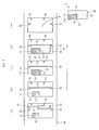
FIGS. 3 illustrate a hoop material used in a manufacturing method according to an embodiment of the present invention.FIG. 3(a) illustrates a state after a punching step,FIG. 3(b) illustrates a state after a bending step,FIG. 3(c) illustrates a state after a first substrate is injection molded,FIG. 3(d) illustrates a state after a second substrate is injection molded, andFIG. 3(e) illustrates a state after a separating step. -
FIG. 4 is a perspective view of a multiband antenna according to another embodiment of the present invention. - Embodiments of the present invention are described in the following with reference to the drawings.
- As illustrated in
FIG. 1 , amultiband antenna 1 according to an embodiment of the present invention is substantially in the shape of a rectangular parallelepiped as a whole. Themultiband antenna 1 comprises afirst antenna unit 10 and asecond antenna unit 20, which are integral with each other. Thefirst antenna unit 10 comprises afirst antenna pattern 11 formed of a conductor and a first substrate 12 (illustrated as a densely dotted area) formed of a dielectric. Thesecond antenna unit 20 comprises asecond antenna pattern 21 formed of a conductor and a second substrate 22 (illustrated as a sparsely dotted area) formed of a dielectric. Themultiband antenna 1 has a length in a longitudinal direction of about 3 to 10 mm. Note that, in the following description, a vertical direction illustrated inFIG. 1 is described as a "vertical direction", but this does not mean to limit the use mode of themultiband antenna 1. - The
first antenna pattern 11 and thesecond antenna pattern 21 are formed of a conductive plate, such as a metal plate, specifically, a copper plate, a steel plate, a SUS plate, a brass plate, or the like. The conductive plate may be plated (for example, gold-plated) as necessary. The conductive plate has a thickness of about- 0.2 to 0.8 mm. Thefirst antenna pattern 11 is provided on a surface of thefirst substrate 12 while thesecond antenna pattern 21 is provided on a surface of the second substrate 22 (seeFIG. 2 ). In order to secure adhesion with respect to thesubstrates antenna patterns substrates FIG. 1 , thefirst antenna pattern 11 is provided only on a side surface on a front side of themultiband antenna 1, and thesecond antenna pattern 21 is provided only on an upper surface of themultiband antenna 1. - Parts of the
antenna patterns first antenna pattern 11 protrudes downward from thefirst substrate 12, and the protruding portion functions as afeeding terminal portion 11a. Afeeding terminal portion 21a is provided at one end of thesecond antenna pattern 21 in the longitudinal direction. Feeders (not shown) are connected to thefeeding terminal portions - The
first substrate 12 is formed of a dielectric, for example, a resin or ceramic. Thefirst substrate 12 of this embodiment is an injection molded product of a resin with thefirst antenna pattern 11 being an insert component. In the illustrated example, the surface of thefirst substrate 12 and the surface of thefirst antenna pattern 11 are flush with each other. Thefirst substrate 12 is formed of, for example, a resin having a dielectric constant of 4 or more. Specifically, as a base resin, for example, polyphenylene sulfide (PPS), a liquid crystal polymer (LCP), or the like may be used. Further, a filler to be mixed in the resin is not specifically limited, and, for example, ceramic may be mixed. Note that, the resin having a dielectric constant of 4 or more is not limited to a resin having a base resin dielectric constant of 4 or more, and a resin having a dielectric constant of 4 or more as a whole through mixture of the filler is also included. - The
second substrate 22 is formed of a dielectric having a dielectric constant different from that of thefirst substrate 12. Thesecond substrate 22 of this embodiment is an injection molded product of a resin with the first antenna unit 10 (first antenna pattern 11 and first substrate 12) and thesecond antenna pattern 21 being insert components. In the illustrated example, the surface of thesecond substrate 22 and the surface of thesecond antenna pattern 21 are flush with each other. Note that, specific examples of a material of thesecond substrate 22 are similar to those of thefirst substrate 12, and thus, description thereof is omitted in order to avoid redundancy. - Next, a method of manufacturing the above-mentioned
multiband antenna 1 is described with reference toFIGS. 3 . Themultiband antenna 1 is manufactured through (a) a punching step, (b) a bending step, (c) a first injection molding-step, (d) a second injection molding step, and (e) a separating step in this order. - First, in the punching step, the conductive plate is punched into a predetermined shape using a punching press die (not shown). Specifically, as illustrated in
FIG. 3(a) , aplanar development shape 31 is formed in which thefirst antenna pattern 11 and thesecond antenna pattern 21 are developed in a plane. In this embodiment, a conductive plate (hoop material 30) in the shape of a long plate is punched so that a plurality of the planar development shapes 31 are arranged in a longitudinal direction. Theplanar development shape 31 is connected to aframe 33 of thehoop material 30 viabridges 32. - Then, the
hoop material 30 is fed in a direction shown by an arrow inFIG. 3 to supply theplanar development shape 31 to the bending step. In the bending step, theplanar development shape 31 in thehoop material 30 is bent with a bending press die (not shown) to form thefirst antenna pattern 11 and thesecond antenna pattern 21 in predetermined shapes (seeFIG. 3(b) ). The bending step is carried out under a state in which thefirst antenna pattern 11 and thesecond antenna pattern 21 are coupled to theframe 33 of thehoop material 30 via thebridges 32. Note that, when theplanar development shape 31 is bent, some of thebridges 32 are separated from the antenna patterns, but each of the antenna patterns is connected to theframe 33 via at least onebridge 32. In the illustrated example, thefirst antenna pattern 11 is connected to theframe 33 of thehoop material 30 via onebridge 32, and thesecond antenna pattern 21 is connected to theframe 33 of thehoop material 30 via twobridges 32 provided on both ends in the longitudinal direction thereof. This enables thefirst antenna pattern 11 and thesecond antenna pattern 21 to be bent keeping the state of being integrated with thehoop material 30. Note that, the bending step may be carried out by pressing once, or may be carried out by pressing a plurality of times. - Then, the
hoop material 30 is further fed to supply thefirst antenna pattern 11 and thesecond antenna pattern 21 to the injection molding step. In this embodiment, by carrying out the first injection molding step of forming thefirst substrate 12 and the second injection molding step of forming thesecond substrate 22 in this order, thefirst substrate 12 and thesecond substrate 22 are formed through double molding. Specifically, first, under a state in which thefirst antenna pattern 11 is placed as an insert component in a cavity of a first injection molding mold (not shown), a resin is injected into the cavity to form thefirst substrate 12. This forms the first antenna unit 10 (first injection molding step, seeFIG. 3(c) ). Then, thehoop material 30 is further fed, and, under a state in which thefirst antenna unit 10 and thesecond antenna pattern 21 are placed in a cavity of a second injection molding mold (not shown), a resin is injected into the cavity to form thesecond substrate 22. This forms thesecond antenna unit 20, and at the same time, thefirst antenna unit 10 and thesecond antenna unit 20 are integrated (second injection molding step, seeFIG. 3(d) ). - Finally, in the separating step, the molded product (multiband antenna 1) is separated from the
frame 33 of the hoop material 30 (seeFIG. 3 (e) ). In the illustrated example, thebridge 32 for connecting thefirst antenna pattern 11 and theframe 33 is cut on a root side (frame 33 side) so as to be integrated with thefirst antenna pattern 11, and thisbridge 32 functions as the feedingterminal portion 11a. Themultiband antenna 1 may be separated from thehoop material 30 soon after the injection molding step, or the molded product may be temporarily wound together with thehoop material 30. By winding themultiband antenna 1 together with thehoop material 30, not only storage and conveyance thereof are easy but also the state of themultiband antennas 1 in alignment with one another can be maintained to prevent interference of themultiband antennas 1. - In the manufacturing steps described above, by carrying out pressing with the bending press die and clamping of the first and second injection molding molds by a common driving unit (press machine), the necessity of providing separate driving units for the respective molds can be eliminated to simplify the system. Further, by carrying out the bending with the bending press die and clamping of the first and second injection molding molds at the same time, cycle time can be cut.
- The present invention is not limited to the above-mentioned embodiment. Now, description is made of other embodiments of the present invention. Parts having the same functions as those in the above-mentioned embodiment are denoted by the same reference symbols, and redundant description thereof is omitted.
- For example, in the above-mentioned bending step, when bending operation is in two stages or when, after the conductive plate is bent with the bending press die, the conductive plate is required to be further bent, the conductive plate may be bent by an actuator (not shown) provided separately from the clamping force on the first and second injecting molding molds. The actuator may be provided inside the bending press die, or may be provided outside the bending press die. As the actuator, for example, an air cylinder, a hydraulic cylinder, a motor, or the like may be used.
- Further, in the embodiment described above, the
antenna patterns substrates - Further, in the embodiment described above, a case is described in which the multiband antenna is formed of two antenna units (
first antenna unit 10 and second antenna unit 20), but the present invention is not limited thereto, and the multiband antenna may be formed of three or more antenna units (not shown). - Further, in the embodiment described above, a case is described in which each of the
first antenna pattern 11 and thesecond antenna pattern 21 is provided on one side surface of themultiband antenna 1, but the present invention is not limited thereto, and each of the antenna patterns may be provided on a plurality of side surfaces. Further, in the embodiment described above, a case is described in which each of thefirst antenna pattern 11 and thesecond antenna pattern 21 is formed of a continuous conductor, but each of the antenna patterns may be formed of a plurality of separate conductors. For example, in amultiband antenna 40 illustrated inFIG. 4 , thefirst antenna pattern 11 is formed of one conductive plate that is continuous over a plurality of side surfaces, and thesecond antenna pattern 21 is formed of a conductive plate that is continuous over a plurality of side surfaces and a plurality of conductive plates separated therefrom. Themultiband antenna 1 can be manufactured by, for example, after the conductive plate (planar development shape 31) is bent to form thefirst antenna pattern 11 and thesecond antenna pattern 21 each having a three-dimensional shape in the bending step, carrying out the first injection molding step and the second injection molding step with the three-dimensional antenna patterns - Further, in the embodiment described above, a case is described in which the
substrates antenna patterns hoop material 30, but the present invention is not limited thereto. For example, thefirst antenna unit 10 may be formed in a separate step, and thesecond antenna unit 20 may be formed by injection molding thesecond substrate 22 with thefirst antenna unit 10 being an insert component. In this case, thefirst substrate 12 of thefirst antenna unit 10 may be formed of a material that is not suitable for injection molding, for example, ceramic. -
- 1
- multiband antenna
- 10
- first antenna unit
- 11
- first antenna pattern
- 12
- first substrate
- 20
- second antenna unit
- 21
- second antenna pattern
- 22
- second substrate
- 30
- hoop material
Claims (6)
- A multiband antenna, comprising:a first antenna unit comprising:a first antenna pattern formed of a conductor; anda first substrate formed of a dielectric, for holding the first antenna pattern; anda second antenna unit comprising:a second antenna pattern formed of a conductor; anda second substrate formed of a dielectric having a dielectric constant different from the dielectric constant of the first substrate, for holding the second antenna pattern,wherein, by injection molding the second substrate with the first antenna unit and the second antenna pattern, which being insert components, the first antenna unit and the second antenna unit are integrated.
- The multiband antenna according to claim 1, wherein the first antenna unit is formed by injection molding the first substrate with the first antenna pattern, which being an insert component.
- The multiband antenna according to claim 2, wherein the first substrate and the second substrate are formed through double molding of resins having different dielectric constants.
- A method of manufacturing a multiband antenna, the multiband antenna comprising:a first antenna unit comprising:a first antenna pattern formed of a conductor; anda first substrate formed of a dielectric, for holding the first antenna pattern; anda second antenna unit comprising:a second antenna pattern formed of a conductor; anda second substrate formed of a dielectric having a dielectric constant different from the dielectric constant of the first substrate, for holding the second antenna pattern, the method comprising the steps of:forming the first antenna unit; andintegrating the first antenna unit and the second antenna unit by injection molding the second substrate with the first antenna unit and the second antenna pattern, which being insert components.
- The method of manufacturing a multiband antenna according to claim 4, wherein the forming the first antenna unit comprises injection molding the first substrate with the first antenna pattern, which being an insert component.
- The method of manufacturing a multiband antenna according to claim 5, further comprising forming the first substrate and the second substrate through double molding of resins having different dielectric constants.
Applications Claiming Priority (2)
| Application Number | Priority Date | Filing Date | Title |
|---|---|---|---|
| JP2012060231A JP6033560B2 (en) | 2012-03-16 | 2012-03-16 | Multiband antenna and manufacturing method thereof |
| PCT/JP2013/057251 WO2013137404A1 (en) | 2012-03-16 | 2013-03-14 | Multiband antenna and manufacturing method thereof |
Publications (2)
| Publication Number | Publication Date |
|---|---|
| EP2827452A1 true EP2827452A1 (en) | 2015-01-21 |
| EP2827452A4 EP2827452A4 (en) | 2015-11-04 |
Family
ID=49161307
Family Applications (1)
| Application Number | Title | Priority Date | Filing Date |
|---|---|---|---|
| EP13761978.9A Withdrawn EP2827452A4 (en) | 2012-03-16 | 2013-03-14 | Multiband antenna and manufacturing method thereof |
Country Status (6)
| Country | Link |
|---|---|
| US (1) | US9912056B2 (en) |
| EP (1) | EP2827452A4 (en) |
| JP (1) | JP6033560B2 (en) |
| CN (1) | CN104205499A (en) |
| IN (1) | IN2014DN07717A (en) |
| WO (1) | WO2013137404A1 (en) |
Families Citing this family (5)
| Publication number | Priority date | Publication date | Assignee | Title |
|---|---|---|---|---|
| JP2015185881A (en) * | 2014-03-20 | 2015-10-22 | Ntn株式会社 | chip antenna |
| US11030507B2 (en) | 2017-11-29 | 2021-06-08 | Phoenix Solution Co., Ltd. | Antenna for RF tag, and RF tag |
| US10658765B2 (en) * | 2018-06-28 | 2020-05-19 | Intel Corporation | Edge-firing antenna walls built into substrate |
| KR20220168507A (en) * | 2021-06-16 | 2022-12-23 | 주식회사 케이엠더블유 | Dual polarization antenna and dual polarization antenna assembly including the same |
| CN117175194A (en) * | 2022-05-26 | 2023-12-05 | 华为技术有限公司 | Multi-band integrated antennas and wireless communication equipment |
Family Cites Families (39)
| Publication number | Priority date | Publication date | Assignee | Title |
|---|---|---|---|---|
| JPS6123423A (en) * | 1984-07-11 | 1986-01-31 | Matsushita Electric Ind Co Ltd | Portable radio equipment |
| JPH0750508A (en) * | 1993-08-06 | 1995-02-21 | Fujitsu Ltd | Antenna module |
| CA2341736A1 (en) | 1999-09-09 | 2001-03-15 | Murata Manufacturing Co | Surface-mounted antenna and communication device compprising the antenna |
| JP2001332929A (en) * | 2000-03-17 | 2001-11-30 | Tdk Corp | Circularly polarized wave patch antenna device |
| EP1237225A1 (en) * | 2001-03-01 | 2002-09-04 | Red-M (Communications) Limited | An antenna array |
| JP2002299936A (en) | 2001-03-29 | 2002-10-11 | Ngk Spark Plug Co Ltd | Chip antenna |
| DE60211889T2 (en) * | 2001-04-23 | 2007-06-14 | Yokowo Co., Ltd. | BROADBAND ANTENNA FOR WIRELESS COMMUNICATION |
| US6618014B2 (en) * | 2001-09-28 | 2003-09-09 | Centurion Wireless Tech., Inc. | Integral antenna and radio system |
| JP2003142936A (en) * | 2001-11-05 | 2003-05-16 | Tdk Corp | Batch antenna |
| JP2003158415A (en) * | 2001-11-20 | 2003-05-30 | Ntn Corp | Equipment with radio communication function |
| JP3895175B2 (en) * | 2001-12-28 | 2007-03-22 | Ntn株式会社 | Dielectric resin integrated antenna |
| JP2005080229A (en) | 2003-09-03 | 2005-03-24 | Mitsubishi Materials Corp | Chip antenna and manufacturing method thereof |
| JP4149357B2 (en) * | 2003-11-06 | 2008-09-10 | 株式会社ヨコオ | Compound antenna |
| JP2005341224A (en) | 2004-05-27 | 2005-12-08 | Matsushita Electric Ind Co Ltd | Antenna device and manufacturing method thereof |
| US7271769B2 (en) * | 2004-09-22 | 2007-09-18 | Lenovo (Singapore) Pte Ltd. | Antennas encapsulated within plastic display covers of computing devices |
| JP2005130532A (en) | 2005-02-08 | 2005-05-19 | Matsushita Electric Ind Co Ltd | Double resonance type dielectric antenna and in-vehicle wireless device |
| US7183983B2 (en) * | 2005-04-26 | 2007-02-27 | Nokia Corporation | Dual-layer antenna and method |
| US7728773B2 (en) * | 2005-10-11 | 2010-06-01 | Ace Antenna Corp. | Multi-band antenna |
| JP4948033B2 (en) * | 2006-05-16 | 2012-06-06 | ローム株式会社 | Microfluidic circuit manufacturing method and microfluidic circuit manufactured by the method |
| US8587480B2 (en) | 2006-08-31 | 2013-11-19 | Amotech Co., Ltd. | Patch antenna and manufacturing method thereof |
| DE102007043409A1 (en) * | 2006-09-15 | 2008-03-27 | Samsung Electro-Mechanics Co., Ltd., Suwon | Method for producing a housing structure with antenna |
| US7545330B2 (en) * | 2006-12-04 | 2009-06-09 | Kabushiki Kaisha Toshiba | Antenna device including surface-mounted element |
| EP1930216A1 (en) | 2006-12-07 | 2008-06-11 | Nederlandse Organisatie voor toegepast-natuurwetenschappelijk Onderzoek TNO | Wire beam |
| WO2008102950A1 (en) * | 2007-02-22 | 2008-08-28 | Amotech Co., Ltd. | Internal antenna with air gap |
| US7804450B2 (en) * | 2007-07-20 | 2010-09-28 | Laird Technologies, Inc. | Hybrid antenna structure |
| TW200924279A (en) * | 2007-11-23 | 2009-06-01 | Lite On Technology Corp | Antenna carrier for supporting a radiator and device thereof |
| US7768463B2 (en) | 2008-04-16 | 2010-08-03 | Sony Ericsson Mobile Communications Ab | Antenna assembly, printed wiring board and device |
| JP2009278376A (en) | 2008-05-14 | 2009-11-26 | Furukawa Electric Co Ltd:The | Multiband antenna |
| JP4775423B2 (en) * | 2008-09-24 | 2011-09-21 | Tdk株式会社 | Antenna device |
| JP2011077714A (en) * | 2009-09-29 | 2011-04-14 | Tdk Corp | Multiple resonance antenna and communication device |
| KR20110057584A (en) * | 2009-11-24 | 2011-06-01 | (주)맥테크놀러지 | Dielectric antenna device having a pattern formed on a printed circuit board and its manufacturing method |
| CN102088132A (en) * | 2009-12-08 | 2011-06-08 | 深圳富泰宏精密工业有限公司 | Shell of electronic device and manufacturing method thereof |
| JP2011130239A (en) * | 2009-12-18 | 2011-06-30 | Tdk Corp | Double resonant antenna, method for manufacturing the same, and communication device |
| US8723736B2 (en) * | 2010-12-06 | 2014-05-13 | Samsung Electronics Co., Ltd | Multi band antenna with multi layers |
| WO2013012403A1 (en) * | 2011-07-15 | 2013-01-24 | Research In Motion Limited | Diversity antenna module and associated method for a user equipment (ue) device |
| US9153856B2 (en) * | 2011-09-23 | 2015-10-06 | Apple Inc. | Embedded antenna structures |
| US8896489B2 (en) * | 2012-05-18 | 2014-11-25 | Nokia Corporation | Antenna |
| US9337532B2 (en) * | 2012-09-18 | 2016-05-10 | Futurewei Technologies, Inc. | Multi layer 3D antenna carrier arrangement for electronic devices |
| KR102077065B1 (en) * | 2013-02-19 | 2020-02-14 | 삼성디스플레이 주식회사 | Window assembly for display device including antenna and manufacturing method thereof |
-
2012
- 2012-03-16 JP JP2012060231A patent/JP6033560B2/en not_active Expired - Fee Related
-
2013
- 2013-03-14 CN CN201380013266.3A patent/CN104205499A/en active Pending
- 2013-03-14 EP EP13761978.9A patent/EP2827452A4/en not_active Withdrawn
- 2013-03-14 US US14/384,884 patent/US9912056B2/en not_active Expired - Fee Related
- 2013-03-14 WO PCT/JP2013/057251 patent/WO2013137404A1/en not_active Ceased
- 2013-03-14 IN IN7717DEN2014 patent/IN2014DN07717A/en unknown
Also Published As
| Publication number | Publication date |
|---|---|
| EP2827452A4 (en) | 2015-11-04 |
| CN104205499A (en) | 2014-12-10 |
| JP2013197678A (en) | 2013-09-30 |
| IN2014DN07717A (en) | 2015-05-15 |
| US20150061963A1 (en) | 2015-03-05 |
| JP6033560B2 (en) | 2016-11-30 |
| US9912056B2 (en) | 2018-03-06 |
| WO2013137404A1 (en) | 2013-09-19 |
Similar Documents
| Publication | Publication Date | Title |
|---|---|---|
| EP2913988B1 (en) | Housing, electronic device using same, and method for making same | |
| KR101585598B1 (en) | The manufacturing method of the built-in antenna | |
| CN101872889B (en) | Antenna pattern frame and manufacture method thereof and mould | |
| US9912056B2 (en) | Multiband antenna and manufacturing method thereof | |
| US20100039347A1 (en) | Housing functioning as an antenna and method for fabricating the same | |
| EP2672567A1 (en) | Antenna device | |
| CN102263322A (en) | Antenna radiator, method of manufacturing electronic device housing, and electronic device housing | |
| JP2012044654A (en) | Case body for electronic equipment and method of manufacturing the same | |
| US20110148716A1 (en) | Multiple resonance antenna, manufacturing method therefor and communication device | |
| KR101025964B1 (en) | Method for manufacturing antenna pattern frame and apparatus | |
| US9634384B2 (en) | Chip antenna and manufacturing method thereof | |
| KR20020053015A (en) | Small antenna and manufacturing method thereof | |
| WO2017047380A1 (en) | Chip antenna and method for producing same | |
| EP3121896A1 (en) | Chip antenna | |
| KR100681597B1 (en) | Chip antenna and manufacturing method of the same | |
| KR100841236B1 (en) | Manufacturing method of SMC type chip antenna using LTC | |
| US10079426B2 (en) | Chip antenna | |
| EP3322264A1 (en) | High frequency module | |
| CN105938937A (en) | Radiator frame and mold for manufacturing the same | |
| CN101651252A (en) | Dual-frequency antenna |
Legal Events
| Date | Code | Title | Description |
|---|---|---|---|
| PUAI | Public reference made under article 153(3) epc to a published international application that has entered the european phase |
Free format text: ORIGINAL CODE: 0009012 |
|
| 17P | Request for examination filed |
Effective date: 20141010 |
|
| AK | Designated contracting states |
Kind code of ref document: A1 Designated state(s): AL AT BE BG CH CY CZ DE DK EE ES FI FR GB GR HR HU IE IS IT LI LT LU LV MC MK MT NL NO PL PT RO RS SE SI SK SM TR |
|
| AX | Request for extension of the european patent |
Extension state: BA ME |
|
| DAX | Request for extension of the european patent (deleted) | ||
| RA4 | Supplementary search report drawn up and despatched (corrected) |
Effective date: 20151006 |
|
| RIC1 | Information provided on ipc code assigned before grant |
Ipc: H01Q 1/42 20060101ALI20151012BHEP Ipc: H01Q 1/40 20060101ALI20151012BHEP Ipc: H01Q 5/22 20150101ALI20151012BHEP Ipc: H01Q 1/38 20060101ALI20151012BHEP Ipc: B29C 45/16 20060101ALI20151012BHEP Ipc: B29C 45/14 20060101ALI20151012BHEP Ipc: H01Q 21/30 20060101AFI20151012BHEP |
|
| 17Q | First examination report despatched |
Effective date: 20180515 |
|
| STAA | Information on the status of an ep patent application or granted ep patent |
Free format text: STATUS: THE APPLICATION HAS BEEN WITHDRAWN |
|
| 18W | Application withdrawn |
Effective date: 20180608 |