EP2827441A1 - Directional coupler - Google Patents
Directional coupler Download PDFInfo
- Publication number
- EP2827441A1 EP2827441A1 EP12871488.8A EP12871488A EP2827441A1 EP 2827441 A1 EP2827441 A1 EP 2827441A1 EP 12871488 A EP12871488 A EP 12871488A EP 2827441 A1 EP2827441 A1 EP 2827441A1
- Authority
- EP
- European Patent Office
- Prior art keywords
- directional coupler
- line
- dielectric substrate
- sub
- directivity
- Prior art date
- Legal status (The legal status is an assumption and is not a legal conclusion. Google has not performed a legal analysis and makes no representation as to the accuracy of the status listed.)
- Granted
Links
Images



Classifications
-
- H—ELECTRICITY
- H01—ELECTRIC ELEMENTS
- H01P—WAVEGUIDES; RESONATORS, LINES, OR OTHER DEVICES OF THE WAVEGUIDE TYPE
- H01P5/00—Coupling devices of the waveguide type
- H01P5/12—Coupling devices having more than two ports
- H01P5/16—Conjugate devices, i.e. devices having at least one port decoupled from one other port
- H01P5/18—Conjugate devices, i.e. devices having at least one port decoupled from one other port consisting of two coupled guides, e.g. directional couplers
- H01P5/184—Conjugate devices, i.e. devices having at least one port decoupled from one other port consisting of two coupled guides, e.g. directional couplers the guides being strip lines or microstrips
-
- H—ELECTRICITY
- H01—ELECTRIC ELEMENTS
- H01P—WAVEGUIDES; RESONATORS, LINES, OR OTHER DEVICES OF THE WAVEGUIDE TYPE
- H01P5/00—Coupling devices of the waveguide type
- H01P5/12—Coupling devices having more than two ports
- H01P5/16—Conjugate devices, i.e. devices having at least one port decoupled from one other port
- H01P5/18—Conjugate devices, i.e. devices having at least one port decoupled from one other port consisting of two coupled guides, e.g. directional couplers
- H01P5/184—Conjugate devices, i.e. devices having at least one port decoupled from one other port consisting of two coupled guides, e.g. directional couplers the guides being strip lines or microstrips
- H01P5/185—Edge coupled lines
Definitions
- the embodiment of the present invention relates to a directional coupler used in a power amplifier for high-power transmission in a digital television transmitter.
- a directional coupler is conventionally provided using a microstrip line structure.
- a pattern of a main line and a pattern of a sub-line are formed on the front surface of a dielectric substrate which has a conductive ground on its rear surface.
- a coupled line which partly constitutes the sub-lines has an appropriate length, and is formed on the substrate in a manner such that there is a micro-space from the main line.
- the length of a coupled line is generally a quarter-wavelength ( ⁇ /4) of a transmit signal detected from a main line in order to obtain optimal directivity.
- ⁇ /4 quarter-wavelength
- a quarter-wavelength ( ⁇ /4) in the UHF band is long, and thus, a circuit tends to be large.
- a loop-coupled line having an appropriate length shorter than a quarter-wavelength ( ⁇ /4) is often used despite a certain level of degradation in directivity.
- Patent Literature 1 Jpn. Pat. Appln. KOKAI Publication No. 7-336117
- An output power level on a transmission path is high in an apparatus of transmitting a high-power signal, such as a power amplifier for a digital television transmitter, therefore, during the detection of high-power, the directivity (isolation property) of a directional coupler is of great concern.
- a compact-size directional coupler that is capable of improving directivity has been desired.
- the purpose of the present embodiment is to provide a directional coupler with high directivity and in a compact size.
- the directional coupler includes a dielectric substrate, a main line formed on the front surface of the dielectric substrate, a sub-line formed on the front surface or the rear surface of the dielectric substrate and placed with a predetermined gap from the main line in the plan view of the dielectric substrate, and an opening provided between the main line and the sub-line through the dielectric substrate.
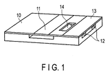
- FIG. 1 is a perspective view of the directional coupler according to the present embodiment.
- FIG. 1 shows an example of the directional coupler used in a high-power amplifier for a terrestrial digital television transmitter.
- FIG. 2 (a) is a plan view of the directional coupler illustrated in FIG. 1
- FIG. 2(b) is a cross-sectional view of the directional coupler with respect to the cross section A-A'. Note that a shield 15 is omitted in FIG. 1 .
- a main line 11 is arranged on the front surface of a dielectric substrate 10, and a sub-line 12 is formed on the rear surface of the dielectric substrate 10, and is placed with a predetermined space from the main line 11 in the plan view of the dielectric substrate.
- a ground surface 13 of the sub-line 12 is formed on the front surface of the dielectric substrate 10 in a manner such that the ground surface 13 is superposed on the sub-line 12. Taking power withstand characteristic into account, a suspended line structure is adopted for the main line 11 as the structure allows a wider line width.
- a microstrip structure is adopted for the sub-line 12. It is possible to arrange the sub-line 12 on the front surface of the dielectric substrate 10 by replacing the sub-line 12 with the ground surface 13.
- an opening 14 is provided between the main line 11 and the sub-line 12.
- the opening 14 is formed through the dielectric substrate 10.
- the width W and the length L of the opening 14, the distance D1 between the main line 11 and the opening 14, and the distance D2 between the opening 14 to the coupling line part of the sub-line 12 are optimized using electromagnetic field simulation.
- the main line 11 and the sub-line 12 are arranged in a manner such that they are opposed to each other with the dielectric substrate 10 therebetween, and since the dielectric substrate 10 is surrounded by the air, the even-mode phase velocity is faster than the odd-mode phase velocity; as a result, directivity is degraded.
- the phase velocities of even and odd modes can be approximated by providing the opening 14 to eliminate part of the dielectric substrate 10. As a consequence, it is possible to improve directivity of the directional coupler.
- FIG. 3 shows a simulation result of the directional coupler according to the present embodiment.
- FIG. 4 the configuration of the directional coupler according to a comparison example is illustrated in FIG. 4 for the purpose of comparison with the present embodiment.
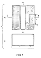
- FIG. 5 (a) is a plan view of the directional coupler shown in FIG. 4
- FIG. 5(b) is a cross-sectional view of the directional coupler with respect to the cross section B-B'.
- the directional coupler of the comparison example is the same as the directional coupler according to the present embodiment, except for the opening 14.
- the length of the coupled line is Lc ( ⁇ ⁇ /4), and a distance to the main line is Dc. Coupling is determined by Dc.
- a loop antenna-shaped lining which is shorter than ⁇ /4 is widely used for the coupling line of a directional coupler.
- this leads to degradation of directivity of the directional coupler because the phase propagation velocities of even and odd modes are different.
- directivity may be further degraded in a case of a weak connection due to a loose coupling.
- FIG. 6 shows a simulation result of the directional coupler shown in FIG. 4 . It can be understood that if the directivity D is calculated by the expression (1) using the result shown in FIG. 6 , the directivity of 11 dB or so can be obtained.
- the directivity of the directional coupler according to the present embodiment is improved by 20 dB compared to the comparison example; accordingly, even if the coupled line part of the sub-line 12 is shorter than ⁇ /4, sufficient directivity can be achieved. Therefore, it can be understood that directivity of the directional coupler can be improved by providing the opening 14.
- directivity can be improved in the present embodiment by providing an opening for adjustment between a main line and a sub-line.
- High directivity can be achieved even when a coupled line is shorter than ⁇ /4. Therefore, according to the present embodiment, it is possible to realize a directional coupler with high directivity in a compact size.
- the directional coupler is provided in an output transmit path of a high power amplifier for a digital television transmitter in the UHF (ultra-high frequency) band. It is placed between a synthesized output and an output connector of a power amplifier to be used as a circuit for detecting an output level and a reflection level of an output power.
- UHF ultra-high frequency
Landscapes
- Transmitters (AREA)
- Amplifiers (AREA)
- Variable-Direction Aerials And Aerial Arrays (AREA)
Abstract
Description
- The embodiment of the present invention relates to a directional coupler used in a power amplifier for high-power transmission in a digital television transmitter.
- A directional coupler is conventionally provided using a microstrip line structure. A pattern of a main line and a pattern of a sub-line (a directional coupler) are formed on the front surface of a dielectric substrate which has a conductive ground on its rear surface. A coupled line which partly constitutes the sub-lines has an appropriate length, and is formed on the substrate in a manner such that there is a micro-space from the main line.
- It is known that the length of a coupled line (a distance between a coupling port and an isolation port) is generally a quarter-wavelength (λ/4) of a transmit signal detected from a main line in order to obtain optimal directivity. However, a quarter-wavelength (λ/4) in the UHF band is long, and thus, a circuit tends to be large. To avoid this, a loop-coupled line having an appropriate length shorter than a quarter-wavelength (λ/4) is often used despite a certain level of degradation in directivity.
- Patent Literature 1: Jpn. Pat. Appln. KOKAI Publication No.
7-336117 - An output power level on a transmission path is high in an apparatus of transmitting a high-power signal, such as a power amplifier for a digital television transmitter, therefore, during the detection of high-power, the directivity (isolation property) of a directional coupler is of great concern. Thus, a compact-size directional coupler that is capable of improving directivity has been desired.
- The purpose of the present embodiment is to provide a directional coupler with high directivity and in a compact size.
- The directional coupler according to the present embodiment includes a dielectric substrate, a main line formed on the front surface of the dielectric substrate, a sub-line formed on the front surface or the rear surface of the dielectric substrate and placed with a predetermined gap from the main line in the plan view of the dielectric substrate, and an opening provided between the main line and the sub-line through the dielectric substrate.
-
-
FIG. 1 is a perspective view of the directional coupler according to the present embodiment. -
FIG. 2 is a plan view and a cross-sectional view of the directional coupler illustrated inFIG. 1 . -
FIG. 3 shows a simulation result of the directional coupler shown inFIG. 1 . -
FIG. 4 is a perspective view of the directional coupler according to a comparison example. -
FIG. 5 is a plan view and a cross-sectional view of the directional coupler illustrated inFIG. 4 . -
FIG. 6 shows a simulation result of the directional coupler shown inFIG. 4 . - In the following, the directional coupler according to the present embodiment will be described in detail with reference to the drawings.
-
FIG. 1 is a perspective view of the directional coupler according to the present embodiment.FIG. 1 shows an example of the directional coupler used in a high-power amplifier for a terrestrial digital television transmitter.FIG. 2 (a) is a plan view of the directional coupler illustrated inFIG. 1 , andFIG. 2(b) is a cross-sectional view of the directional coupler with respect to the cross section A-A'. Note that ashield 15 is omitted inFIG. 1 . - A
main line 11 is arranged on the front surface of adielectric substrate 10, and asub-line 12 is formed on the rear surface of thedielectric substrate 10, and is placed with a predetermined space from themain line 11 in the plan view of the dielectric substrate. Aground surface 13 of thesub-line 12 is formed on the front surface of thedielectric substrate 10 in a manner such that theground surface 13 is superposed on thesub-line 12. Taking power withstand characteristic into account, a suspended line structure is adopted for themain line 11 as the structure allows a wider line width. A microstrip structure is adopted for thesub-line 12. It is possible to arrange thesub-line 12 on the front surface of thedielectric substrate 10 by replacing thesub-line 12 with theground surface 13. - Furthermore, an
opening 14 is provided between themain line 11 and thesub-line 12. Theopening 14 is formed through thedielectric substrate 10. The width W and the length L of theopening 14, the distance D1 between themain line 11 and theopening 14, and the distance D2 between theopening 14 to the coupling line part of thesub-line 12 are optimized using electromagnetic field simulation. - Herein, the effect of the
opening 14 is explained. Themain line 11 and thesub-line 12 are arranged in a manner such that they are opposed to each other with thedielectric substrate 10 therebetween, and since thedielectric substrate 10 is surrounded by the air, the even-mode phase velocity is faster than the odd-mode phase velocity; as a result, directivity is degraded. In contrast, in the present embodiment the phase velocities of even and odd modes can be approximated by providing the opening 14 to eliminate part of thedielectric substrate 10. As a consequence, it is possible to improve directivity of the directional coupler. -
FIG. 3 shows a simulation result of the directional coupler according to the present embodiment. As shown in the expression (1) below, directivity D of the directional coupler can be calculated by the difference of a coupling I of a coupling port P3 relative to an input port P1 and a coupling C of an isolation port P4 relative to an input port P1, i.e.,
- It can be understood that if the directivity D is calculated by the expression (1) using the result shown in
FIG. 3 , the directivity of 31 dB or so can be obtained. "S2, 1" inFIG. 3 corresponds to I, and "S3, 1" corresponds to C. - Herein, the configuration of the directional coupler according to a comparison example is illustrated in
FIG. 4 for the purpose of comparison with the present embodiment.FIG. 5 (a) is a plan view of the directional coupler shown inFIG. 4 , andFIG. 5(b) is a cross-sectional view of the directional coupler with respect to the cross section B-B'. The directional coupler of the comparison example is the same as the directional coupler according to the present embodiment, except for theopening 14. - In
FIG. 5 (a) , the length of the coupled line is Lc (< λ/4), and a distance to the main line is Dc. Coupling is determined by Dc. Generally, a loop antenna-shaped lining which is shorter than λ/4 is widely used for the coupling line of a directional coupler. However, this leads to degradation of directivity of the directional coupler because the phase propagation velocities of even and odd modes are different. Moreover, directivity may be further degraded in a case of a weak connection due to a loose coupling. -
FIG. 6 shows a simulation result of the directional coupler shown inFIG. 4 . It can be understood that if the directivity D is calculated by the expression (1) using the result shown inFIG. 6 , the directivity of 11 dB or so can be obtained. - Comparing
FIG. 3 withFIG. 6 , the directivity of the directional coupler according to the present embodiment is improved by 20 dB compared to the comparison example; accordingly, even if the coupled line part of thesub-line 12 is shorter than λ/4, sufficient directivity can be achieved. Therefore, it can be understood that directivity of the directional coupler can be improved by providing theopening 14. - As explained above, directivity can be improved in the present embodiment by providing an opening for adjustment between a main line and a sub-line. High directivity can be achieved even when a coupled line is shorter than λ/4. Therefore, according to the present embodiment, it is possible to realize a directional coupler with high directivity in a compact size.
- As an example of one of the applications of the directional coupler according to the present embodiment, the directional coupler is provided in an output transmit path of a high power amplifier for a digital television transmitter in the UHF (ultra-high frequency) band. It is placed between a synthesized output and an output connector of a power amplifier to be used as a circuit for detecting an output level and a reflection level of an output power.
- While certain embodiments have been described, these embodiments have been presented by way of example only, and are not intended to limit the scope of the inventions. Indeed, the novel embodiments described herein may be embodied in a variety of other forms; furthermore, various omissions, substitutions, and changes in the form of the embodiments described herein may be made without departing from the spirit of the inventions. The accompanying claims and their equivalents are intended to cover such forms or modifications as would fall within the scope and spirit of the inventions.
Claims (2)
- A directional coupler characterized by comprising:a dielectric substrate;a main line formed on a front surface of the dielectric substrate;a sub-line formed on the front surface or a rear surface of the dielectric substrate, the sub-line being placed with a predetermined gap from the main line in the plan view of the dielectric substrate; andan opening provided between the main line and the sub-line through the dielectric substrate.
- The directional coupler according to claim 1, characterized in that a length of the sub-line is shorter than λ/4 with respect to a wavelength λ of a transmit signal detected at the main line.
Applications Claiming Priority (2)
| Application Number | Priority Date | Filing Date | Title |
|---|---|---|---|
| JP2012057525A JP5439527B2 (en) | 2012-03-14 | 2012-03-14 | Directional coupler |
| PCT/JP2012/073664 WO2013136557A1 (en) | 2012-03-14 | 2012-09-14 | Directional coupler |
Publications (3)
| Publication Number | Publication Date |
|---|---|
| EP2827441A1 true EP2827441A1 (en) | 2015-01-21 |
| EP2827441A4 EP2827441A4 (en) | 2015-11-04 |
| EP2827441B1 EP2827441B1 (en) | 2019-10-23 |
Family
ID=49160513
Family Applications (1)
| Application Number | Title | Priority Date | Filing Date |
|---|---|---|---|
| EP12871488.8A Active EP2827441B1 (en) | 2012-03-14 | 2012-09-14 | Directional coupler |
Country Status (4)
| Country | Link |
|---|---|
| EP (1) | EP2827441B1 (en) |
| JP (1) | JP5439527B2 (en) |
| CN (1) | CN104137328B (en) |
| WO (1) | WO2013136557A1 (en) |
Cited By (2)
| Publication number | Priority date | Publication date | Assignee | Title |
|---|---|---|---|---|
| RU188691U1 (en) * | 2019-02-07 | 2019-04-22 | Федеральное государственное автономное образовательное учреждение высшего образования "Санкт-Петербургский государственный университет аэрокосмического приборостроения" | Striped coupler |
| US10547095B2 (en) | 2016-11-29 | 2020-01-28 | Kabushiki Kaisha Toshiba | Method of manufacturing directional coupler |
Families Citing this family (1)
| Publication number | Priority date | Publication date | Assignee | Title |
|---|---|---|---|---|
| CN112034224B (en) * | 2020-08-25 | 2023-07-14 | 中国电子科技集团公司第三十六研究所 | A coupled detector |
Family Cites Families (9)
| Publication number | Priority date | Publication date | Assignee | Title |
|---|---|---|---|---|
| US2951218A (en) * | 1957-02-19 | 1960-08-30 | Itt | Directional couplings |
| JPS62114301A (en) * | 1985-11-13 | 1987-05-26 | Mitsubishi Electric Corp | Suspended line type directional coupler |
| JP2768411B2 (en) * | 1991-09-30 | 1998-06-25 | 宇部興産株式会社 | Dielectric waveguide directional coupler |
| JPH07336117A (en) | 1994-06-13 | 1995-12-22 | Murata Mfg Co Ltd | Directional coupler |
| KR100339373B1 (en) * | 1998-10-13 | 2002-07-18 | 구자홍 | micro strip coupler and method for fabricating the same |
| JP4181083B2 (en) * | 2003-12-24 | 2008-11-12 | 三菱電機株式会社 | Plating method and high frequency line |
| JP4356628B2 (en) * | 2005-02-25 | 2009-11-04 | 日本電気株式会社 | Directional coupler |
| FI124514B (en) * | 2006-05-12 | 2014-09-30 | Filtronic Comtek Oy | The directional coupler |
| CN101577358B (en) * | 2009-06-23 | 2013-04-03 | 北京信息科技大学 | Micromechanical terahertz waveguide, terahertz waveguide type resonant cavity and preparation method thereof |
-
2012
- 2012-03-14 JP JP2012057525A patent/JP5439527B2/en active Active
- 2012-09-14 CN CN201280070947.9A patent/CN104137328B/en active Active
- 2012-09-14 EP EP12871488.8A patent/EP2827441B1/en active Active
- 2012-09-14 WO PCT/JP2012/073664 patent/WO2013136557A1/en not_active Ceased
Cited By (2)
| Publication number | Priority date | Publication date | Assignee | Title |
|---|---|---|---|---|
| US10547095B2 (en) | 2016-11-29 | 2020-01-28 | Kabushiki Kaisha Toshiba | Method of manufacturing directional coupler |
| RU188691U1 (en) * | 2019-02-07 | 2019-04-22 | Федеральное государственное автономное образовательное учреждение высшего образования "Санкт-Петербургский государственный университет аэрокосмического приборостроения" | Striped coupler |
Also Published As
| Publication number | Publication date |
|---|---|
| CN104137328A (en) | 2014-11-05 |
| CN104137328B (en) | 2017-03-08 |
| WO2013136557A1 (en) | 2013-09-19 |
| JP5439527B2 (en) | 2014-03-12 |
| EP2827441B1 (en) | 2019-10-23 |
| EP2827441A4 (en) | 2015-11-04 |
| JP2013192084A (en) | 2013-09-26 |
Similar Documents
| Publication | Publication Date | Title |
|---|---|---|
| US10135108B2 (en) | Directional coupler and diplexer | |
| US9929471B2 (en) | Very compact TM01 mode extractor | |
| US8022788B2 (en) | Filter with crosses | |
| CN103117442A (en) | Ridge waveguide directional coupler | |
| US20140273891A1 (en) | Transceiver Arrangement | |
| KR101489538B1 (en) | Omt type broadband multiband transmission-reception coupler-separator for rf frequency telecommunications antennas | |
| CN107732398B (en) | Broadband high-power millimeter wave over-mode waveguide TE01Directional coupler | |
| US9263783B2 (en) | Waveguide circulator having stepped floor/ceiling and quarter-wave dielectric transformer | |
| CN103311612A (en) | Strip-line high-pass filter | |
| EP2827441B1 (en) | Directional coupler | |
| JP5755546B2 (en) | Power combiner / distributor, power amplifier circuit, and radio apparatus | |
| CN208723066U (en) | A kind of micro-strip vertical transition structure | |
| JP6219324B2 (en) | Planar transmission line waveguide converter | |
| JP2008271074A (en) | High frequency coupler | |
| JP6262437B2 (en) | Polarized bandpass filter | |
| US20160087324A1 (en) | Waveguide circulator with improved transition to other transmission line media | |
| KR101619173B1 (en) | Directional Coupler Having valiable Directors | |
| TWI528624B (en) | Balanced tri - band band - pass filter | |
| JP2015207863A (en) | Polarization coupler | |
| JPH05335806A (en) | Dielectric microwave filter | |
| JP2015050491A (en) | High frequency cutoff filter, microwave output device, transmission circuit and radar device | |
| EP2339691B1 (en) | Physically non-uniform TEM-mode directional coupler | |
| KR20120017210A (en) | Open waveguide transitions and horn antennas | |
| CN102403564A (en) | Directional coupler | |
| WO2016079907A1 (en) | Circulator and wireless communication apparatus |
Legal Events
| Date | Code | Title | Description |
|---|---|---|---|
| PUAI | Public reference made under article 153(3) epc to a published international application that has entered the european phase |
Free format text: ORIGINAL CODE: 0009012 |
|
| 17P | Request for examination filed |
Effective date: 20140908 |
|
| AK | Designated contracting states |
Kind code of ref document: A1 Designated state(s): AL AT BE BG CH CY CZ DE DK EE ES FI FR GB GR HR HU IE IS IT LI LT LU LV MC MK MT NL NO PL PT RO RS SE SI SK SM TR |
|
| AX | Request for extension of the european patent |
Extension state: BA ME |
|
| DAX | Request for extension of the european patent (deleted) | ||
| RA4 | Supplementary search report drawn up and despatched (corrected) |
Effective date: 20151007 |
|
| RIC1 | Information provided on ipc code assigned before grant |
Ipc: H01P 5/18 20060101AFI20151001BHEP |
|
| STAA | Information on the status of an ep patent application or granted ep patent |
Free format text: STATUS: EXAMINATION IS IN PROGRESS |
|
| 17Q | First examination report despatched |
Effective date: 20180424 |
|
| GRAP | Despatch of communication of intention to grant a patent |
Free format text: ORIGINAL CODE: EPIDOSNIGR1 |
|
| STAA | Information on the status of an ep patent application or granted ep patent |
Free format text: STATUS: GRANT OF PATENT IS INTENDED |
|
| INTG | Intention to grant announced |
Effective date: 20190408 |
|
| GRAS | Grant fee paid |
Free format text: ORIGINAL CODE: EPIDOSNIGR3 |
|
| GRAA | (expected) grant |
Free format text: ORIGINAL CODE: 0009210 |
|
| STAA | Information on the status of an ep patent application or granted ep patent |
Free format text: STATUS: THE PATENT HAS BEEN GRANTED |
|
| AK | Designated contracting states |
Kind code of ref document: B1 Designated state(s): AL AT BE BG CH CY CZ DE DK EE ES FI FR GB GR HR HU IE IS IT LI LT LU LV MC MK MT NL NO PL PT RO RS SE SI SK SM TR |
|
| REG | Reference to a national code |
Ref country code: GB Ref legal event code: FG4D |
|
| REG | Reference to a national code |
Ref country code: CH Ref legal event code: EP |
|
| REG | Reference to a national code |
Ref country code: IE Ref legal event code: FG4D |
|
| REG | Reference to a national code |
Ref country code: DE Ref legal event code: R096 Ref document number: 602012065165 Country of ref document: DE |
|
| REG | Reference to a national code |
Ref country code: AT Ref legal event code: REF Ref document number: 1194709 Country of ref document: AT Kind code of ref document: T Effective date: 20191115 |
|
| REG | Reference to a national code |
Ref country code: NL Ref legal event code: MP Effective date: 20191023 |
|
| REG | Reference to a national code |
Ref country code: LT Ref legal event code: MG4D |
|
| PG25 | Lapsed in a contracting state [announced via postgrant information from national office to epo] |
Ref country code: PT Free format text: LAPSE BECAUSE OF FAILURE TO SUBMIT A TRANSLATION OF THE DESCRIPTION OR TO PAY THE FEE WITHIN THE PRESCRIBED TIME-LIMIT Effective date: 20200224 Ref country code: BG Free format text: LAPSE BECAUSE OF FAILURE TO SUBMIT A TRANSLATION OF THE DESCRIPTION OR TO PAY THE FEE WITHIN THE PRESCRIBED TIME-LIMIT Effective date: 20200123 Ref country code: FI Free format text: LAPSE BECAUSE OF FAILURE TO SUBMIT A TRANSLATION OF THE DESCRIPTION OR TO PAY THE FEE WITHIN THE PRESCRIBED TIME-LIMIT Effective date: 20191023 Ref country code: LT Free format text: LAPSE BECAUSE OF FAILURE TO SUBMIT A TRANSLATION OF THE DESCRIPTION OR TO PAY THE FEE WITHIN THE PRESCRIBED TIME-LIMIT Effective date: 20191023 Ref country code: LV Free format text: LAPSE BECAUSE OF FAILURE TO SUBMIT A TRANSLATION OF THE DESCRIPTION OR TO PAY THE FEE WITHIN THE PRESCRIBED TIME-LIMIT Effective date: 20191023 Ref country code: SE Free format text: LAPSE BECAUSE OF FAILURE TO SUBMIT A TRANSLATION OF THE DESCRIPTION OR TO PAY THE FEE WITHIN THE PRESCRIBED TIME-LIMIT Effective date: 20191023 Ref country code: NL Free format text: LAPSE BECAUSE OF FAILURE TO SUBMIT A TRANSLATION OF THE DESCRIPTION OR TO PAY THE FEE WITHIN THE PRESCRIBED TIME-LIMIT Effective date: 20191023 Ref country code: ES Free format text: LAPSE BECAUSE OF FAILURE TO SUBMIT A TRANSLATION OF THE DESCRIPTION OR TO PAY THE FEE WITHIN THE PRESCRIBED TIME-LIMIT Effective date: 20191023 Ref country code: NO Free format text: LAPSE BECAUSE OF FAILURE TO SUBMIT A TRANSLATION OF THE DESCRIPTION OR TO PAY THE FEE WITHIN THE PRESCRIBED TIME-LIMIT Effective date: 20200123 Ref country code: PL Free format text: LAPSE BECAUSE OF FAILURE TO SUBMIT A TRANSLATION OF THE DESCRIPTION OR TO PAY THE FEE WITHIN THE PRESCRIBED TIME-LIMIT Effective date: 20191023 Ref country code: GR Free format text: LAPSE BECAUSE OF FAILURE TO SUBMIT A TRANSLATION OF THE DESCRIPTION OR TO PAY THE FEE WITHIN THE PRESCRIBED TIME-LIMIT Effective date: 20200124 |
|
| PG25 | Lapsed in a contracting state [announced via postgrant information from national office to epo] |
Ref country code: HR Free format text: LAPSE BECAUSE OF FAILURE TO SUBMIT A TRANSLATION OF THE DESCRIPTION OR TO PAY THE FEE WITHIN THE PRESCRIBED TIME-LIMIT Effective date: 20191023 Ref country code: IS Free format text: LAPSE BECAUSE OF FAILURE TO SUBMIT A TRANSLATION OF THE DESCRIPTION OR TO PAY THE FEE WITHIN THE PRESCRIBED TIME-LIMIT Effective date: 20200224 Ref country code: RS Free format text: LAPSE BECAUSE OF FAILURE TO SUBMIT A TRANSLATION OF THE DESCRIPTION OR TO PAY THE FEE WITHIN THE PRESCRIBED TIME-LIMIT Effective date: 20191023 |
|
| PG25 | Lapsed in a contracting state [announced via postgrant information from national office to epo] |
Ref country code: AL Free format text: LAPSE BECAUSE OF FAILURE TO SUBMIT A TRANSLATION OF THE DESCRIPTION OR TO PAY THE FEE WITHIN THE PRESCRIBED TIME-LIMIT Effective date: 20191023 |
|
| REG | Reference to a national code |
Ref country code: DE Ref legal event code: R097 Ref document number: 602012065165 Country of ref document: DE |
|
| PG2D | Information on lapse in contracting state deleted |
Ref country code: IS |
|
| PG25 | Lapsed in a contracting state [announced via postgrant information from national office to epo] |
Ref country code: EE Free format text: LAPSE BECAUSE OF FAILURE TO SUBMIT A TRANSLATION OF THE DESCRIPTION OR TO PAY THE FEE WITHIN THE PRESCRIBED TIME-LIMIT Effective date: 20191023 Ref country code: RO Free format text: LAPSE BECAUSE OF FAILURE TO SUBMIT A TRANSLATION OF THE DESCRIPTION OR TO PAY THE FEE WITHIN THE PRESCRIBED TIME-LIMIT Effective date: 20191023 Ref country code: CZ Free format text: LAPSE BECAUSE OF FAILURE TO SUBMIT A TRANSLATION OF THE DESCRIPTION OR TO PAY THE FEE WITHIN THE PRESCRIBED TIME-LIMIT Effective date: 20191023 Ref country code: DK Free format text: LAPSE BECAUSE OF FAILURE TO SUBMIT A TRANSLATION OF THE DESCRIPTION OR TO PAY THE FEE WITHIN THE PRESCRIBED TIME-LIMIT Effective date: 20191023 Ref country code: IS Free format text: LAPSE BECAUSE OF FAILURE TO SUBMIT A TRANSLATION OF THE DESCRIPTION OR TO PAY THE FEE WITHIN THE PRESCRIBED TIME-LIMIT Effective date: 20200223 |
|
| REG | Reference to a national code |
Ref country code: AT Ref legal event code: MK05 Ref document number: 1194709 Country of ref document: AT Kind code of ref document: T Effective date: 20191023 |
|
| PLBE | No opposition filed within time limit |
Free format text: ORIGINAL CODE: 0009261 |
|
| STAA | Information on the status of an ep patent application or granted ep patent |
Free format text: STATUS: NO OPPOSITION FILED WITHIN TIME LIMIT |
|
| PG25 | Lapsed in a contracting state [announced via postgrant information from national office to epo] |
Ref country code: IT Free format text: LAPSE BECAUSE OF FAILURE TO SUBMIT A TRANSLATION OF THE DESCRIPTION OR TO PAY THE FEE WITHIN THE PRESCRIBED TIME-LIMIT Effective date: 20191023 Ref country code: SK Free format text: LAPSE BECAUSE OF FAILURE TO SUBMIT A TRANSLATION OF THE DESCRIPTION OR TO PAY THE FEE WITHIN THE PRESCRIBED TIME-LIMIT Effective date: 20191023 Ref country code: SM Free format text: LAPSE BECAUSE OF FAILURE TO SUBMIT A TRANSLATION OF THE DESCRIPTION OR TO PAY THE FEE WITHIN THE PRESCRIBED TIME-LIMIT Effective date: 20191023 |
|
| 26N | No opposition filed |
Effective date: 20200724 |
|
| PG25 | Lapsed in a contracting state [announced via postgrant information from national office to epo] |
Ref country code: SI Free format text: LAPSE BECAUSE OF FAILURE TO SUBMIT A TRANSLATION OF THE DESCRIPTION OR TO PAY THE FEE WITHIN THE PRESCRIBED TIME-LIMIT Effective date: 20191023 Ref country code: AT Free format text: LAPSE BECAUSE OF FAILURE TO SUBMIT A TRANSLATION OF THE DESCRIPTION OR TO PAY THE FEE WITHIN THE PRESCRIBED TIME-LIMIT Effective date: 20191023 |
|
| PG25 | Lapsed in a contracting state [announced via postgrant information from national office to epo] |
Ref country code: MC Free format text: LAPSE BECAUSE OF FAILURE TO SUBMIT A TRANSLATION OF THE DESCRIPTION OR TO PAY THE FEE WITHIN THE PRESCRIBED TIME-LIMIT Effective date: 20191023 |
|
| REG | Reference to a national code |
Ref country code: CH Ref legal event code: PL |
|
| REG | Reference to a national code |
Ref country code: BE Ref legal event code: MM Effective date: 20200930 |
|
| PG25 | Lapsed in a contracting state [announced via postgrant information from national office to epo] |
Ref country code: LU Free format text: LAPSE BECAUSE OF NON-PAYMENT OF DUE FEES Effective date: 20200914 |
|
| PG25 | Lapsed in a contracting state [announced via postgrant information from national office to epo] |
Ref country code: FR Free format text: LAPSE BECAUSE OF NON-PAYMENT OF DUE FEES Effective date: 20200930 |
|
| PG25 | Lapsed in a contracting state [announced via postgrant information from national office to epo] |
Ref country code: IE Free format text: LAPSE BECAUSE OF NON-PAYMENT OF DUE FEES Effective date: 20200914 Ref country code: LI Free format text: LAPSE BECAUSE OF NON-PAYMENT OF DUE FEES Effective date: 20200930 Ref country code: CH Free format text: LAPSE BECAUSE OF NON-PAYMENT OF DUE FEES Effective date: 20200930 Ref country code: BE Free format text: LAPSE BECAUSE OF NON-PAYMENT OF DUE FEES Effective date: 20200930 |
|
| PG25 | Lapsed in a contracting state [announced via postgrant information from national office to epo] |
Ref country code: TR Free format text: LAPSE BECAUSE OF FAILURE TO SUBMIT A TRANSLATION OF THE DESCRIPTION OR TO PAY THE FEE WITHIN THE PRESCRIBED TIME-LIMIT Effective date: 20191023 Ref country code: MT Free format text: LAPSE BECAUSE OF FAILURE TO SUBMIT A TRANSLATION OF THE DESCRIPTION OR TO PAY THE FEE WITHIN THE PRESCRIBED TIME-LIMIT Effective date: 20191023 Ref country code: CY Free format text: LAPSE BECAUSE OF FAILURE TO SUBMIT A TRANSLATION OF THE DESCRIPTION OR TO PAY THE FEE WITHIN THE PRESCRIBED TIME-LIMIT Effective date: 20191023 |
|
| PG25 | Lapsed in a contracting state [announced via postgrant information from national office to epo] |
Ref country code: MK Free format text: LAPSE BECAUSE OF FAILURE TO SUBMIT A TRANSLATION OF THE DESCRIPTION OR TO PAY THE FEE WITHIN THE PRESCRIBED TIME-LIMIT Effective date: 20191023 |
|
| PGFP | Annual fee paid to national office [announced via postgrant information from national office to epo] |
Ref country code: DE Payment date: 20250702 Year of fee payment: 14 |
|
| PGFP | Annual fee paid to national office [announced via postgrant information from national office to epo] |
Ref country code: GB Payment date: 20250703 Year of fee payment: 14 |