EP2825931B1 - Master-slave interface - Google Patents
Master-slave interface Download PDFInfo
- Publication number
- EP2825931B1 EP2825931B1 EP13760302.3A EP13760302A EP2825931B1 EP 2825931 B1 EP2825931 B1 EP 2825931B1 EP 13760302 A EP13760302 A EP 13760302A EP 2825931 B1 EP2825931 B1 EP 2825931B1
- Authority
- EP
- European Patent Office
- Prior art keywords
- bus
- bcl
- slave
- interrupt
- condition
- Prior art date
- Legal status (The legal status is an assumption and is not a legal conclusion. Google has not performed a legal analysis and makes no representation as to the accuracy of the status listed.)
- Not-in-force
Links
Images


Classifications
-
- G—PHYSICS
- G06—COMPUTING OR CALCULATING; COUNTING
- G06F—ELECTRIC DIGITAL DATA PROCESSING
- G06F13/00—Interconnection of, or transfer of information or other signals between, memories, input/output devices or central processing units
- G06F13/38—Information transfer, e.g. on bus
- G06F13/42—Bus transfer protocol, e.g. handshake; Synchronisation
- G06F13/4282—Bus transfer protocol, e.g. handshake; Synchronisation on a serial bus, e.g. I2C bus, SPI bus
-
- G—PHYSICS
- G06—COMPUTING OR CALCULATING; COUNTING
- G06F—ELECTRIC DIGITAL DATA PROCESSING
- G06F13/00—Interconnection of, or transfer of information or other signals between, memories, input/output devices or central processing units
- G06F13/38—Information transfer, e.g. on bus
- G06F13/42—Bus transfer protocol, e.g. handshake; Synchronisation
-
- G—PHYSICS
- G06—COMPUTING OR CALCULATING; COUNTING
- G06F—ELECTRIC DIGITAL DATA PROCESSING
- G06F13/00—Interconnection of, or transfer of information or other signals between, memories, input/output devices or central processing units
- G06F13/38—Information transfer, e.g. on bus
- G06F13/40—Bus structure
- G06F13/4063—Device-to-bus coupling
- G06F13/4068—Electrical coupling
- G06F13/4081—Live connection to bus, e.g. hot-plugging
Definitions
- BIF Battery InterFace
- a glitch may occur between a battery pack and host device.
- Document US6789136 B1 presents a requesting device which sends a request, intended to read one or more device addresses on a line of a bus.
- a read bit timing diagram is presented, which starts by the requesting device driving the bus line to a high voltage level for a predetermined time while the other devices are not driving the line.
- the originator in this case the requesting device, then releases the line, i.e. presents a high impedance to it, upon lapsing of the predetermined time.
- the responding devices having recognized the read command, then hold the signal level at a high voltage following the timing rules.
- an additional event or side signal line is provided. This event line is used for interrupting the system.
- a device is configured to include an EN/SET input pin. Holding the EN/SET pin high causes the device to maintain its operational state. Holding the EN/SET pin low for a predetermined timeout period resets the counter and causes the device to adopt a predetermined configuration (such as off) until new clock pulses are received at the EN/SET pin.
- a slave when a slave exits a mode upon detecting a transition on a bus, it drives the bus at the transition level for an extended duration, ensuring that other components on the bus detect the extended duration level.
- this causes the low pulse on the bus to be extended (no use but no harm).
- this basically extends the glitch and allows others (including the master) to detect the condition, avoiding the need for the master to conduct periodic polling.
- the master may send a command, such as an enable interrupt command, at a slower speed and thus increase the ⁇ BIF time.
- a command such as an enable interrupt command
- the master may be implemented in a way that it can detect short contact breaks. This optional feature may protect against a longer contact break that overlaps the whole extended glitch driven by the slave.
- Some variations of the invention include a master and slave system (and components thereof) that perform various functions such as those described above, and a memory or other computer-readable medium having stored therein instruction which, when executed, perform functions such as those described above.
- a host device 101 e.g., a mobile phone
- a battery pack 102 is coupled to a battery pack 102 through a set of paired connectors VBAT (battery voltage), BCL (battery communication line), and GND (ground).
- the host device 101 may comprise a master communication unit 103, whereas the battery pack 102 may comprise one or more slave units 106.
- Battery pack 102 also includes a battery cell 107, which is coupled to the host device 101 through connectors VBAT and GND to supply power to host device 101.
- other slave units may also be coupled to BCL within host device 101 and/or in other battery packs.
- Communication between the host device 101 and battery pack 102 is performed over the single BCL line by switching the BCL to GND.
- Master 103 transmits data by activating switch 108 (via processor 104 or another circuit component within host device 101), whereas slave 106 transmits data by activating switch 112 (via processor 114).
- Data is received in each unit over the BCL and may be passed through respective Schmitt triggers 111 and 113 to help with noise suppression on the BCL bus.
- Processors 104 and 114 in each unit may execute instructions to transmit and receive data over the bus.
- Host device 101 may also include one or more other components, such as RF integrated circuit 105, for performing functions such as communicating over a wireless network.
- Signaling (e.g., data transmission) between host device 101 and battery pack 102 is based on the elapsed time between changes of signal level on the BCL. Bits are transmitted by modulating the duration between signal toggles, similar to pulse-width modulation.
- the BIF specification refers to this as Time Distance Coding).
- the duration of the short bit is ⁇ BIF
- the duration of the long bit is 3 ⁇ BIF
- ⁇ BIF is the BIF time base.
- the BIF time base is defined by the master for every data word with a training sequence. Each word begins with a training sequence, which provides a fixed reference period of 4 ⁇ BIF between two falling edges, to calibrate the slave timing to the transmission speed.
- the master may choose any ⁇ BIF within specified boundaries, and it may change the ⁇ BIF used from one data word to another. Communication is initiated by the master, and the communication speed is set by the master. The slave adapts to the speed on each command and uses the same speed when replying.
- the master 103 has a pull-up resistor 109 (in active communication typically a few kilo-Ohms, in idle mode typically a few hundred kilo-Ohms) on the bus.
- the slave 106 has a pull-down resistor 110 typically varying between 240 kOhm to 450 kOhm for detecting the battery type and the battery removal.
- the slave's pull-down resistor 110 has a resistance R ID that may be sensed by host device 101 as a voltage divider in order to determine battery capacity, battery type, or other parameters.
- the BCL bus may be in one of four modes: Active, Standby, Power-down, or Interrupt mode.
- the Interrupt mode is used when waiting for an interrupt event generated by a slave.
- the Interrupt mode is entered when the master sends an enable interrupt (EINT) command on the BCL, allowing any slave devices coupled to BCL to initiate an interrupt to master device 103.
- EINT enable interrupt
- host device 101 polls registers in each slave device to determine what interrupt occurred and, based on the interrupt, handles it appropriately.
- the Interrupt mode ends when either of the following conditions occurs:
- a glitch may occur on the communication line BCL due to movement of the battery pack, causing a short disconnection at the battery connector. Because of the pull-down resistor 110 in the battery pack, the BCL line at the slave side goes low during the glitch, which may cause the slave to incorrectly detect Condition 2. Because the master has the pull-up resistor 109, the BCL line stays high at the host side and thus the glitch, and more importantly, the exit condition of the Interrupt Mode, is never seen by the master.
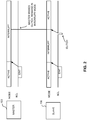
- master 103 and slave 106 are initially in Active mode. After a period of time, master 103 issues an EINT command on the BCL, which causes both the master and slave to enter the Interrupt mode. After a second period of time, a glitch on the BCL is seen by the slave, causing it to exit the interrupt mode and re-enter the Active mode. However, the master 103 may not detect the glitch, so it remains in interrupt mode. This mismatched situation leads the master to continue waiting indefinitely for an interrupt, whereas the slave or slaves will not generate interrupts because they have switched to Active mode.
- This situation may affect most seriously the use case where the slave is used to continuously monitor the battery temperature via a temperature sensing function using its threshold capability (i.e. generating an interrupt when temperature is outside the given window).
- the master must exit the Interrupt mode periodically, check the condition of the slaves, and re-enter the Interrupt mode. This may increase power consumption and require processor time.
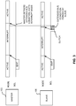
- FIG. 3 illustrates a method for extending a detected condition on a bus, such as a glitch, in accordance with some variations of the invention.
- a master device 103 and slave device 106 begin in Active mode, and the master 103 issues an enable interrupt command EINT, causing both the master and slave to transition to the Interrupt mode.
- Other slaves on the bus (not shown) also transition to the Interrupt mode.
- the slave may detect the transition on the bus and, according to certain variations, the slave extends the bus condition (e.g., holding the bus down to ground) for an extended period of time, ensuring that the master detects the transition. Thereafter, both the master and the slave transition to the Active mode.
- the bus condition e.g., holding the bus down to ground
- the slave may extend the bus condition for a sufficiently long time that it can be reasonably certain that other devices on the bus will interpret the pulse as an interrupt command. For example, very short pulses can be extended to at least ⁇ BIF duration, and possibly to a multiple of ⁇ BIF . If the glitch is "long" (e.g., as long as or longer than ⁇ BIF ), the slave may not need to extend the bus condition at all, because it can be reasonably certain that other devices on the bus will interpret it as an interrupt command.
- circuitry similar to that used to detect battery removal may be used to detect the short voltage spikes.
- a digital filter may send a short contact interrupt immediately when a comparator detects a voltage above the battery removal threshold.
- circuitry may be configured to detect that current from the host to slave decreases, signaling a contact break. Other variations are of course possible.
- the bus's voltage level is based on the voltage divider R_up/ R_down.
- the R down disappears and thus the bus voltage goes close to the pull-up voltage, i.e. higher than the logic 1. If these short contact breaks are detected and indicated to the master via an interrupt, then the host may be able to recover faster from a potential error condition. Thus, according to some variations, the host may see one or both of the following events when there is a short contact break in the battery communication line:
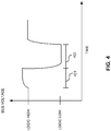
- FIG. 4 shows an example of a bus voltage during a contact break as seen on the master side of the bus, including a first time period 401 during which the bus voltage is a short pulse that is briefly higher than a logic 1 level.
- a detected voltage level that exceeds a valid logic level on the bus is treated as an out-of-variance bus condition that causes further action, as described below.
- the bus level is driven low for an extended period of time by the slave unit, such as due to an interrupt.
- the host may first wait for the bus to settle, then create a wake-up pulse if the bus was previously in non-Active mode to wake up the slaves, then check that it can communicate with the slaves.
- the host may proceed as with a normal interrupt (e.g., check interrupt source, process the interrupt if any, and re-enable interrupts).
- the normal interrupt process at the host side comprises the following: First, the host gets the interrupt pulse (which may be the extended glitch).
- the host reads the Interrupt Status registers (IRQ_STS) of each slave, using a command (for example) specified in the BIF specification. If there are interrupts, they are processed and the IRQ_STS flags are reset. Finally, the bus may be ordered back to interrupt mode using the EINT command.
- IRQ_STS Interrupt Status registers
- event 402 should cover event 401 as well. That is, the bus does not need a separate wake-up as a low pulse was detected, and the communication check can be accomplished implicitly when reading the interrupt status registers.
- Detecting short contact breaks at the host may also be used in other situations, for example in the Power Down or Standby states, in which short contact breaks might wake up a slave device. Because normally the host would not detect the breaks, detecting the short high pulse can be used to determine that a slave may have awakened, causing the host to again set it to sleep mode or ordering it into a different mode.
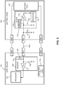
- FIG. 5 illustrates a battery interface incorporating various features described herein.
- the arrangement shown in FIG. 5 is similar to that shown in FIG. 1 , except that the host device and slave device have been augmented with certain functions that perform as explained above.
- battery pack 102 includes a driver circuit 115 that drives bus BCL by extending a bus condition detected on the bus.
- driver circuit 115 may hold down the BCL line for a minimum time period sufficient to trigger a mode change in master 103.
- Driver circuit 115 may be implemented in software (e.g., a memory of processor 114), such that when processor 114 detects a low pulse on the BCL bus, it instructs driver circuit 115 to force the BCL bus low for a predetermined period of time, extending the detected bus condition.
- driver circuit 115 may be implemented as a separate circuit with analog and/or digital components.
- bus detect and logic circuit 116 which as explained above may detect a voltage level higher than a predetermined value (e.g., high logic level) on the BCL bus. In response to the detection, bus detect and logic circuit 116 may issue a command to one or more slaves, wherein the command causes the slaves to enter a different mode or state.
- a predetermined value e.g., high logic level
- bus detect and logic circuit 116 may issue a command to one or more slaves, wherein the command causes the slaves to enter a different mode or state.
- the functions of circuit 116 may be incorporated into processor 104 and its associated memory storing instructions (not shown), or they may be implemented in a separate circuit. As with the slave circuitry discussed above, this circuitry may detect the condition in various ways.
- the host when the host detects that the battery pack is sinking less current than the highest allowed battery resistor value, the host may interpret this as a contact break or battery removal.
- these means may include means for processing or analyzing data, means for detecting conditions on a bus, means for communicating via a bus, means for driving a voltage level of a bus, means for communicating by modulating a duration of signal levels on a bus, means for transitioning between modes associated with a device, and/or means for receiving or transmitting commands.
- the master may send a command, such as an enable interrupt command, at a slower speed and thus increase the ⁇ BIF time.
- a command such as an enable interrupt command
- the specification allows the master to choose a communication speed for each word.
- the master may choose a speed for the enable interrupt command that is slower than most or all speeds selected for other words and commands used on the bus.
- ASICs application-specific integrated circuits
- FPGAs field-programmable gate arrays
- One or more tangible computer-readable media such as one or more memories, may store executable instructions that, when executed by one or more processors, perform the functions described herein.
- FIG. 6 illustrates a flow chart including steps and functions that may be carried out in certain variations of the invention.
- a slave in a master-slave system detects a bus condition, such as a low voltage level on the bus.
- the slave forces an extended bus condition. In some variations, this may include forcing a low voltage level on the bus for an extended time duration (e.g., a predetermined minimum duration corresponding to a mode change signal), causing other devices on the bus to interpret the forced condition as a mode change.
- an extended time duration e.g., a predetermined minimum duration corresponding to a mode change signal
- the slave may determine whether the forced condition constitutes a mode change to the slave device. For example, if the slave was originally in an Interrupt mode, it may transition to an Active mode. Other examples of modes that the slave may transition to include Standby mode and Power-down mode. If the forced condition corresponds to a mode change, then in step 604 the slave changes to the new mode.
- the master detects the extended bus condition on the bus. For example, the master may detect that the voltage level on a BCL bus has been held low for a sufficient period of time so as to signal a mode change. As one example, if the master was originally in an Interrupt mode, it may transition to an Active mode based on the extended bus condition. Other examples of modes that the master may transition to include Standby mode and Power-down mode.
- the master may determine whether it should transition to a different mode. If the forced condition corresponds to a mode change, then in step 607 the master changes to the new mode.
- step 608 the process may end.
- the master may detect an out-of-variance bus condition. For example, the master may detect a voltage spike that is higher than a specified range and duration for logic 1 level. Such a spike might be generated, for example, by a battery pack being connected, disconnected, or jostled, causing a short voltage spike on the bus.
- the master in response to detecting the out-of-variance bus condition, may take action to change the bus state to a stable condition. For example, the master may issue one or more commands to slaves on the bus, such as a command to change to a different mode. For example, the master may command the slaves to reset, to stand by, to power down, and/or to enter other modes as described above.
- step 611 the slaves on the bus change modes in response to the commands issued by the master.
Landscapes
- Engineering & Computer Science (AREA)
- Theoretical Computer Science (AREA)
- General Engineering & Computer Science (AREA)
- Physics & Mathematics (AREA)
- General Physics & Mathematics (AREA)
- Computer Hardware Design (AREA)
- Power Sources (AREA)
- Secondary Cells (AREA)
- Small-Scale Networks (AREA)
Description
- Mobile devices, such as cellular telephones, laptop computers, e-readers, and personal digital assistants, all use batteries in order to be portable. In recent years, the Mobile Industry Processor Interface (MIPI) Alliance has developed a standard interface between batteries and mobile devices. The Battery InterFace (BIF) specification defines an electrical and communication interface between batteries and mobile devices. The BIF specification supports both low-cost batteries and so-called "smart" batteries that contain active elements for handling security features (e.g., authentication) and other more advanced battery functions such as temperature monitoring.
- In some situations, a glitch may occur between a battery pack and host device.
- Document
US6789136 B1 presents a requesting device which sends a request, intended to read one or more device addresses on a line of a bus. A read bit timing diagram is presented, which starts by the requesting device driving the bus line to a high voltage level for a predetermined time while the other devices are not driving the line. The originator, in this case the requesting device, then releases the line, i.e. presents a high impedance to it, upon lapsing of the predetermined time. The responding devices, having recognized the read command, then hold the signal level at a high voltage following the timing rules. In an embodiment, an additional event or side signal line is provided. This event line is used for interrupting the system. - Document
US 2003/0188202 A1 presents a single wire serial interface for power ICs and other devices. To use the interface, a device is configured to include an EN/SET input pin. Holding the EN/SET pin high causes the device to maintain its operational state. Holding the EN/SET pin low for a predetermined timeout period resets the counter and causes the device to adopt a predetermined configuration (such as off) until new clock pulses are received at the EN/SET pin. - This section presents a brief summary of some variations of the invention. It is not intended to identify critical or required elements of the invention. The invention may be practiced without incorporating many or all of the features described in this section.
- The invention is defined by the appended claims.
- In some variations, when a slave exits a mode upon detecting a transition on a bus, it drives the bus at the transition level for an extended duration, ensuring that other components on the bus detect the extended duration level. In the glitch-free case (e.g., a real interrupt), this causes the low pulse on the bus to be extended (no use but no harm). In a glitch case, this basically extends the glitch and allows others (including the master) to detect the condition, avoiding the need for the master to conduct periodic polling.
- In some variations, the master may send a command, such as an enable interrupt command, at a slower speed and thus increase the τBIF time. This has two effects. First, the duration of the glitch that causes the issue in the first place may be reduced. Second, this may extend the time the slave drives the bus low, and thus may be easier to detect by the master.
- Optionally, the master may be implemented in a way that it can detect short contact breaks. This optional feature may protect against a longer contact break that overlaps the whole extended glitch driven by the slave.
- Some variations of the invention include a master and slave system (and components thereof) that perform various functions such as those described above, and a memory or other computer-readable medium having stored therein instruction which, when executed, perform functions such as those described above.
-
-
FIG. 1 illustrates an exemplary battery interface including electrical connections between ahost device 101 and abattery pack 102. -
FIG. 2 illustrates an example of a glitch that may cause a slave to exit a first mode without a master detecting that the mode was exited. -
FIG. 3 illustrates an exemplary method for extending a detected condition on a bus. -
FIG. 4 shows an example of a bus voltage during a contact break as seen on the master side of the bus. -
FIG. 5 illustrates an exemplary battery interface incorporating various features described herein. -
FIG. 6 illustrates an exemplary flow chart including steps and functions that may be carried out in certain variations of the invention. - In reference to the OSI reference model, the BIF specification defines both physical and data link layers. As shown in
FIG. 1 , a host device 101 (e.g., a mobile phone) is coupled to abattery pack 102 through a set of paired connectors VBAT (battery voltage), BCL (battery communication line), and GND (ground). Thehost device 101 may comprise amaster communication unit 103, whereas thebattery pack 102 may comprise one ormore slave units 106.Battery pack 102 also includes abattery cell 107, which is coupled to thehost device 101 through connectors VBAT and GND to supply power tohost device 101. Although not shown inFIG. 1 , other slave units may also be coupled to BCL withinhost device 101 and/or in other battery packs. - Communication between the
host device 101 andbattery pack 102 is performed over the single BCL line by switching the BCL to GND.Master 103 transmits data by activating switch 108 (viaprocessor 104 or another circuit component within host device 101), whereasslave 106 transmits data by activating switch 112 (via processor 114). Data is received in each unit over the BCL and may be passed through respective Schmitttriggers Processors Host device 101 may also include one or more other components, such as RF integratedcircuit 105, for performing functions such as communicating over a wireless network. - Signaling (e.g., data transmission) between
host device 101 andbattery pack 102 is based on the elapsed time between changes of signal level on the BCL. Bits are transmitted by modulating the duration between signal toggles, similar to pulse-width modulation. (The BIF specification refers to this as Time Distance Coding). The duration of the short bit is τBIF, and the duration of the long bit is 3τBIF ,where τBIF is the BIF time base. The BIF time base is defined by the master for every data word with a training sequence. Each word begins with a training sequence, which provides a fixed reference period of 4τBIF between two falling edges, to calibrate the slave timing to the transmission speed. - The master may choose any τBIF within specified boundaries, and it may change the τBIF used from one data word to another. Communication is initiated by the master, and the communication speed is set by the master. The slave adapts to the speed on each command and uses the same speed when replying.
- The
master 103 has a pull-up resistor 109 (in active communication typically a few kilo-Ohms, in idle mode typically a few hundred kilo-Ohms) on the bus. Theslave 106 has a pull-down resistor 110 typically varying between 240 kOhm to 450 kOhm for detecting the battery type and the battery removal. The slave's pull-down resistor 110 has a resistance RID that may be sensed byhost device 101 as a voltage divider in order to determine battery capacity, battery type, or other parameters. - The BCL bus may be in one of four modes: Active, Standby, Power-down, or Interrupt mode. The Interrupt mode is used when waiting for an interrupt event generated by a slave. The Interrupt mode is entered when the master sends an enable interrupt (EINT) command on the BCL, allowing any slave devices coupled to BCL to initiate an interrupt to
master device 103. When an interrupt occurs,host device 101 polls registers in each slave device to determine what interrupt occurred and, based on the interrupt, handles it appropriately. The Interrupt mode ends when either of the following conditions occurs: - Condition 1: When a slave detects an internal interrupt, it drives the BCL bus low for the duration of τBIF and exits the Interrupt mode and enters Active mode.
- Condition 2: When a master or a slave detects the bus low for τBIF duration, it exits the Interrupt mode and enters Active mode.
- A glitch may occur on the communication line BCL due to movement of the battery pack, causing a short disconnection at the battery connector. Because of the pull-
down resistor 110 in the battery pack, the BCL line at the slave side goes low during the glitch, which may cause the slave to incorrectly detect Condition 2. Because the master has the pull-upresistor 109, the BCL line stays high at the host side and thus the glitch, and more importantly, the exit condition of the Interrupt Mode, is never seen by the master. - Turning to
FIG. 2 ,master 103 andslave 106 are initially in Active mode. After a period of time,master 103 issues an EINT command on the BCL, which causes both the master and slave to enter the Interrupt mode. After a second period of time, a glitch on the BCL is seen by the slave, causing it to exit the interrupt mode and re-enter the Active mode. However, themaster 103 may not detect the glitch, so it remains in interrupt mode. This mismatched situation leads the master to continue waiting indefinitely for an interrupt, whereas the slave or slaves will not generate interrupts because they have switched to Active mode. - This situation may affect most seriously the use case where the slave is used to continuously monitor the battery temperature via a temperature sensing function using its threshold capability (i.e. generating an interrupt when temperature is outside the given window).
- If the interrupt mode cannot be trusted, the master must exit the Interrupt mode periodically, check the condition of the slaves, and re-enter the Interrupt mode. This may increase power consumption and require processor time.
-
FIG. 3 illustrates a method for extending a detected condition on a bus, such as a glitch, in accordance with some variations of the invention. Like the situation illustrated inFIG. 2 , amaster device 103 andslave device 106 begin in Active mode, and themaster 103 issues an enable interrupt command EINT, causing both the master and slave to transition to the Interrupt mode. Other slaves on the bus (not shown) also transition to the Interrupt mode. - When a glitch occurs, the slave may detect the transition on the bus and, according to certain variations, the slave extends the bus condition (e.g., holding the bus down to ground) for an extended period of time, ensuring that the master detects the transition. Thereafter, both the master and the slave transition to the Active mode.
- In some variations, the slave may extend the bus condition for a sufficiently long time that it can be reasonably certain that other devices on the bus will interpret the pulse as an interrupt command. For example, very short pulses can be extended to at least τBIF duration, and possibly to a multiple of τBIF. If the glitch is "long" (e.g., as long as or longer than τBIF), the slave may not need to extend the bus condition at all, because it can be reasonably certain that other devices on the bus will interpret it as an interrupt command.
- In some variations, circuitry similar to that used to detect battery removal may be used to detect the short voltage spikes. For example, a digital filter may send a short contact interrupt immediately when a comparator detects a voltage above the battery removal threshold. In other variations, circuitry may be configured to detect that current from the host to slave decreases, signaling a contact break. Other variations are of course possible.
- In a normal state, the bus's voltage level is based on the voltage divider R_up/ R_down. On a contact break, the R down disappears and thus the bus voltage goes close to the pull-up voltage, i.e. higher than the logic 1. If these short contact breaks are detected and indicated to the master via an interrupt, then the host may be able to recover faster from a potential error condition. Thus, according to some variations, the host may see one or both of the following events when there is a short contact break in the battery communication line:
- 1. An extended glitch (
FIG. 3 ). This is detected by the host as a normal interrupt exit condition. - 2. A short pulse that is higher than logic 1 (
FIG. 4 ). This may be detected by the host as an interrupt signal from a voltage comparator, for example. -
FIG. 4 shows an example of a bus voltage during a contact break as seen on the master side of the bus, including afirst time period 401 during which the bus voltage is a short pulse that is briefly higher than a logic 1 level. In some variations, a detected voltage level that exceeds a valid logic level on the bus is treated as an out-of-variance bus condition that causes further action, as described below. During asecond time period 402, the bus level is driven low for an extended period of time by the slave unit, such as due to an interrupt. - Upon detecting the out-of-variance bus condition 401 (e.g., a detected voltage level that exceeds a valid logic level on the bus), the host may first wait for the bus to settle, then create a wake-up pulse if the bus was previously in non-Active mode to wake up the slaves, then check that it can communicate with the slaves. Upon detecting the interrupt 402, the host may proceed as with a normal interrupt (e.g., check interrupt source, process the interrupt if any, and re-enable interrupts). The normal interrupt process at the host side comprises the following: First, the host gets the interrupt pulse (which may be the extended glitch). Second, the host reads the Interrupt Status registers (IRQ_STS) of each slave, using a command (for example) specified in the BIF specification. If there are interrupts, they are processed and the IRQ_STS flags are reset. Finally, the bus may be ordered back to interrupt mode using the EINT command.
- If
events event 402 should coverevent 401 as well. That is, the bus does not need a separate wake-up as a low pulse was detected, and the communication check can be accomplished implicitly when reading the interrupt status registers. - Detecting short contact breaks at the host may also be used in other situations, for example in the Power Down or Standby states, in which short contact breaks might wake up a slave device. Because normally the host would not detect the breaks, detecting the short high pulse can be used to determine that a slave may have awakened, causing the host to again set it to sleep mode or ordering it into a different mode.
-
FIG. 5 illustrates a battery interface incorporating various features described herein. The arrangement shown inFIG. 5 is similar to that shown inFIG. 1 , except that the host device and slave device have been augmented with certain functions that perform as explained above. Starting with the right side ofFIG. 5 ,battery pack 102 includes adriver circuit 115 that drives bus BCL by extending a bus condition detected on the bus. As explained above, for example,driver circuit 115 may hold down the BCL line for a minimum time period sufficient to trigger a mode change inmaster 103.Driver circuit 115 may be implemented in software (e.g., a memory of processor 114), such that whenprocessor 114 detects a low pulse on the BCL bus, it instructsdriver circuit 115 to force the BCL bus low for a predetermined period of time, extending the detected bus condition. Alternatively,driver circuit 115 may be implemented as a separate circuit with analog and/or digital components. - The left side of
FIG. 5 shows thathost device 101 includes a bus detect andlogic circuit 116, which as explained above may detect a voltage level higher than a predetermined value (e.g., high logic level) on the BCL bus. In response to the detection, bus detect andlogic circuit 116 may issue a command to one or more slaves, wherein the command causes the slaves to enter a different mode or state. As withdriver 115, the functions ofcircuit 116 may be incorporated intoprocessor 104 and its associated memory storing instructions (not shown), or they may be implemented in a separate circuit. As with the slave circuitry discussed above, this circuitry may detect the condition in various ways. For example, when the host detects that the battery pack is sinking less current than the highest allowed battery resistor value, the host may interpret this as a contact break or battery removal. In general, the above structural elements, or parts thereof, may be seen as means for performing operations to implement one or more embodiments of the invention. For example, these means may include means for processing or analyzing data, means for detecting conditions on a bus, means for communicating via a bus, means for driving a voltage level of a bus, means for communicating by modulating a duration of signal levels on a bus, means for transitioning between modes associated with a device, and/or means for receiving or transmitting commands. - In some variations, the master may send a command, such as an enable interrupt command, at a slower speed and thus increase the τBIF time. For example, the specification allows the master to choose a communication speed for each word. The master may choose a speed for the enable interrupt command that is slower than most or all speeds selected for other words and commands used on the bus.
- This may have two effects. First, the duration of the glitch that causes the issue in the first place may be reduced. Second, this may extend the time the slave drives the bus low, and thus may be easier to detect by the master.
- The functions outlined above in both the master and slave may be implemented in hardware, software, or a combination of the two, including such structures as application-specific integrated circuits (ASICs), field-programmable gate arrays (FPGAs) and other known structures. One or more tangible computer-readable media, such as one or more memories, may store executable instructions that, when executed by one or more processors, perform the functions described herein.
-
FIG. 6 illustrates a flow chart including steps and functions that may be carried out in certain variations of the invention. Starting with the left side ofFIG. 6 , in step 601 a slave in a master-slave system (e.g., a BIF-compliant battery/host system) detects a bus condition, such as a low voltage level on the bus. In response to detecting the bus condition, instep 602 the slave forces an extended bus condition. In some variations, this may include forcing a low voltage level on the bus for an extended time duration (e.g., a predetermined minimum duration corresponding to a mode change signal), causing other devices on the bus to interpret the forced condition as a mode change. - In
step 603, the slave may determine whether the forced condition constitutes a mode change to the slave device. For example, if the slave was originally in an Interrupt mode, it may transition to an Active mode. Other examples of modes that the slave may transition to include Standby mode and Power-down mode. If the forced condition corresponds to a mode change, then instep 604 the slave changes to the new mode. - In
step 605, the master detects the extended bus condition on the bus. For example, the master may detect that the voltage level on a BCL bus has been held low for a sufficient period of time so as to signal a mode change. As one example, if the master was originally in an Interrupt mode, it may transition to an Active mode based on the extended bus condition. Other examples of modes that the master may transition to include Standby mode and Power-down mode. Instep 606, the master may determine whether it should transition to a different mode. If the forced condition corresponds to a mode change, then instep 607 the master changes to the new mode. - In
step 608, the process may end. - The right side of
FIG. 6 illustrates other steps that may be performed by the master and slave. Instep 609, the master may detect an out-of-variance bus condition. For example, the master may detect a voltage spike that is higher than a specified range and duration for logic 1 level. Such a spike might be generated, for example, by a battery pack being connected, disconnected, or jostled, causing a short voltage spike on the bus. - In
step 610, in response to detecting the out-of-variance bus condition, the master may take action to change the bus state to a stable condition. For example, the master may issue one or more commands to slaves on the bus, such as a command to change to a different mode. For example, the master may command the slaves to reset, to stand by, to power down, and/or to enter other modes as described above. - In
step 611, the slaves on the bus change modes in response to the commands issued by the master. - It should be appreciated that the principles described above may have many variations, and the invention is not intended to be limited to the features and variations described herein.
Claims (13)
- A method comprising:receiving, at one or more slave devices (106), a command from the master device (103) to enter an interrupt mode;in response to receiving the command, entering the interrupt mode at the one or more slave devices (106);detecting, by the one or more slave devices (106), a condition on a bus (BCL) that couples a master device and one or more slave devices (106), wherein the master and slave devices (103, 106) communicate by alternating a voltage level on the bus between a low voltage level and a high voltage level;in response to detecting the condition on the bus (BCL), forcing an extension of the condition on the bus (BCL) for a predetermined time period and transitioning the one or more slave devices (106) to a non-interrupt mode.
- The method of claim 1, wherein forcing the extension of the condition on the bus (BCL) comprises driving a voltage level of the bus (BCL) for the predetermined time period.
- The method of claim 1 or 2, wherein the master device (103) and the one or more slave devices (106) communicate by modulating a duration of signal levels on the bus (BCL).
- The method of any of claims 1 to 3, wherein the interrupt mode allows the one or more slave devices (106) to initiate an interrupt to the master device (103), and wherein the extension of the condition on the bus (BCL) for a predetermined time period is forced to causes the master device (103) to exit an interrupt mode, in which the master device (103) waits for an interrupt generated by one or more slave devices (106).
- The method of any of claims 1 to 4, wherein the bus (BCL) comprises a single-wire bus between a host device (101) and one or more battery packs (102).
- The method of any of claims 1 to 5, further comprising, from one of the slave devices (106), generating an interrupt signal on the bus (BCL) when the bus (BCL) is in an interrupt mode.
- The method of claim 6, further comprising, at the master device (103), detecting the interrupt signal from one or more of the slave devices (106) and, in response, processing one or more interrupts based on signals read from the one or more slave devices (106).
- The method of any of claims 1 to 7, wherein forcing the extension of the bus condition is done by one or more of the slave devices (106).
- Apparatus (102) comprising:a bus interface comprising contacts for power and a communication line to couple the apparatus (102) to a bus (BCL); andslave circuitry (112-114) coupled to the bus interface and configured to communicate with a master device (103) over the bus (BCL), wherein the slave circuitry is further configured toreceive a command from the master device (103) to enter an interrupt mode;in response to receiving the command, enter the interrupt mode;detect a condition on the bus (BCL), wherein the master and slave circuitry (108, 109, 111; 112-114) communicate by alternating a voltage level on the bus (BCL) between a low voltage level and a high voltage level; andin response to detecting the condition on the bus (BCL), forcing an extension of the condition on the bus (BCL) for a predetermined time period and transition to a non-interrupt mode.
- The apparatus (102) of claim 9, wherein the slave circuitry (112-114) forces the extension of the condition on the bus (BCL) by driving a voltage level of the bus for the predetermined time period.
- The apparatus (102) of claim 9 or 10, wherein the slave circuitry (112-114) communicates with the master device (103) by modulating a duration of signal levels on the bus (BCL).
- The apparatus (102) of any of claims 9 to 11, wherein the interrupt mode allows the slave circuitry (112-114) to initiate an interrupt to the master device (103), and wherein the extension of the condition on the bus (BCL) for a predetermined time period is forced to causes the master device (103) to exit the interrupt mode, in which the master device (103) waits for an interrupt generated by the slave circuitry (112-114).
- The apparatus (102) of any of claims 9 to 12, wherein the bus (BCL) comprises a single-wire bus between a host device (101) and one or more battery packs (102).
Applications Claiming Priority (2)
| Application Number | Priority Date | Filing Date | Title |
|---|---|---|---|
| US13/418,414 US9015393B2 (en) | 2012-03-13 | 2012-03-13 | Master-slave interface |
| PCT/FI2013/050170 WO2013135946A2 (en) | 2012-03-13 | 2013-02-14 | Master-slave interface |
Publications (3)
| Publication Number | Publication Date |
|---|---|
| EP2825931A2 EP2825931A2 (en) | 2015-01-21 |
| EP2825931A4 EP2825931A4 (en) | 2015-10-28 |
| EP2825931B1 true EP2825931B1 (en) | 2017-11-29 |
Family
ID=49158763
Family Applications (1)
| Application Number | Title | Priority Date | Filing Date |
|---|---|---|---|
| EP13760302.3A Not-in-force EP2825931B1 (en) | 2012-03-13 | 2013-02-14 | Master-slave interface |
Country Status (4)
| Country | Link |
|---|---|
| US (1) | US9015393B2 (en) |
| EP (1) | EP2825931B1 (en) |
| CN (1) | CN104272217B (en) |
| WO (1) | WO2013135946A2 (en) |
Families Citing this family (17)
| Publication number | Priority date | Publication date | Assignee | Title |
|---|---|---|---|---|
| JP6015054B2 (en) * | 2012-03-27 | 2016-10-26 | 株式会社ソシオネクスト | Error response circuit, semiconductor integrated circuit, and data transfer control method |
| TWI518516B (en) * | 2012-11-13 | 2016-01-21 | Novatek Microelectronics Corp | Bus detection and control method and bus detection and control device and mobile industry processor interface system thereof |
| US20140143588A1 (en) * | 2012-11-21 | 2014-05-22 | Nokia Corporation | Instant Communication Error Indication From Slave |
| US9287718B2 (en) * | 2013-03-01 | 2016-03-15 | Nokia Technologies Oy | Method, apparatus, and computer program product for foreign object detection parameter and charging data communication with wireless charging capable battery pack |
| KR102035986B1 (en) * | 2013-11-13 | 2019-10-24 | 삼성전자 주식회사 | Timing controller, and display system including the same |
| US10219208B1 (en) | 2014-08-07 | 2019-02-26 | Ethertronics, Inc. | Heterogeneous network optimization utilizing modal antenna techniques |
| US9883322B2 (en) | 2014-08-07 | 2018-01-30 | Ethertronics, Inc. | Heterogeneous network optimization and organization utilizing modal antenna techniques and master-slave schemes |
| US9755821B2 (en) | 2015-04-02 | 2017-09-05 | Samsung Electronics Co., Ltd. | Device including single wire interface and data processing system including the same |
| KR102328014B1 (en) | 2015-08-24 | 2021-11-18 | 삼성전자주식회사 | Device including single wire interface and data processing system having the same |
| US10855527B2 (en) * | 2018-04-03 | 2020-12-01 | Infineon Technologies Ag | Bidirectional communication using edge timing in a signal |
| US10635630B2 (en) * | 2018-08-09 | 2020-04-28 | Qualcomm Incorporated | Flexible protocol and associated hardware for one-wire radio frequency front-end interface |
| US10887074B1 (en) | 2019-08-02 | 2021-01-05 | Infineon Technologies Ag | Full duplex communication using edge timing in a signal |
| US10958412B1 (en) | 2020-01-22 | 2021-03-23 | Infineon Technologies Ag | Communication using edge timing in a signal |
| JP7415824B2 (en) * | 2020-06-30 | 2024-01-17 | 横河電機株式会社 | Expansion module, CPU module, system, and communication method |
| CN113064845A (en) * | 2021-04-28 | 2021-07-02 | 晶澄微电子(宁波)有限公司 | Method for realizing single-wire communication with anti-counterfeiting security chip |
| CN118369655A (en) | 2022-01-20 | 2024-07-19 | 三星电子株式会社 | Method and electronic device for communicating on a single-wire interface |
| WO2023140703A1 (en) * | 2022-01-20 | 2023-07-27 | Samsung Electronics Co., Ltd. | Method and electronic device for communication on single wire interface |
Family Cites Families (14)
| Publication number | Priority date | Publication date | Assignee | Title |
|---|---|---|---|---|
| US4107651A (en) * | 1976-11-08 | 1978-08-15 | Hewlett-Packard Company | Glitch detector |
| US5177371A (en) | 1990-10-12 | 1993-01-05 | Compaq Computer Corporation | Auxiliary battery operation detection circuit |
| US6275167B1 (en) * | 1998-06-08 | 2001-08-14 | Visteon Global Technologies, Inc. | Method and system for communicating between remote-controlled modules in automotive vehicles |
| DE10003705C2 (en) * | 2000-01-28 | 2003-04-24 | Siemens Ag | Data transmission arrangement and associated method |
| US6789136B1 (en) * | 2000-12-29 | 2004-09-07 | Intel Corporation | Efficient method to obtain device addresses from devices on a bus |
| US6529046B1 (en) * | 2001-12-12 | 2003-03-04 | Etron Technology, Inc. | Minimum pulse width detection and regeneration circuit |
| US7127631B2 (en) * | 2002-03-28 | 2006-10-24 | Advanced Analogic Technologies, Inc. | Single wire serial interface utilizing count of encoded clock pulses with reset |
| KR100965876B1 (en) | 2003-06-03 | 2010-06-24 | 삼성전자주식회사 | Battery charging device using a USB and digital camera having the same |
| US7612472B2 (en) * | 2004-01-23 | 2009-11-03 | American Power Conversion Corporation | Method and apparatus for monitoring energy storage devices |
| US7271568B2 (en) | 2004-02-11 | 2007-09-18 | Research In Motion Limited | Battery charger for portable devices and related methods |
| US20060085653A1 (en) | 2004-10-08 | 2006-04-20 | Apple Computer, Inc. | Method and system for transferring data with respect to a portable electronic device |
| JP4611387B2 (en) * | 2004-12-24 | 2011-01-12 | エルジー・ケム・リミテッド | Voltage balance control system for lithium ion battery and control method thereof |
| US7526589B2 (en) * | 2007-01-23 | 2009-04-28 | International Business Machines Corporation | Apparatus, system, and method for resetting an inter-integrated circuit data line using a negative voltage |
| US8982520B2 (en) * | 2008-09-19 | 2015-03-17 | Standard Microsystems Corporation | USB port overvoltage protection |
-
2012
- 2012-03-13 US US13/418,414 patent/US9015393B2/en not_active Expired - Fee Related
-
2013
- 2013-02-14 CN CN201380024439.1A patent/CN104272217B/en not_active Expired - Fee Related
- 2013-02-14 EP EP13760302.3A patent/EP2825931B1/en not_active Not-in-force
- 2013-02-14 WO PCT/FI2013/050170 patent/WO2013135946A2/en not_active Ceased
Non-Patent Citations (1)
| Title |
|---|
| None * |
Also Published As
| Publication number | Publication date |
|---|---|
| WO2013135946A2 (en) | 2013-09-19 |
| US9015393B2 (en) | 2015-04-21 |
| WO2013135946A3 (en) | 2013-11-07 |
| CN104272217B (en) | 2017-07-28 |
| EP2825931A4 (en) | 2015-10-28 |
| EP2825931A2 (en) | 2015-01-21 |
| CN104272217A (en) | 2015-01-07 |
| US20130246675A1 (en) | 2013-09-19 |
Similar Documents
| Publication | Publication Date | Title |
|---|---|---|
| US9015393B2 (en) | Master-slave interface | |
| US10565145B2 (en) | Felxconnect disconnect detection | |
| US8904054B2 (en) | Method and apparatus for mode switching of interface ports | |
| KR100928905B1 (en) | Accessory control interface | |
| EP2534496B1 (en) | Determination of physical connectivity status of devices based on electrical measurement | |
| EP2808755B1 (en) | Method and apparatus for handling a charging state in a mobile electronic device | |
| US9018896B2 (en) | Method and system for determining whether a portable device is charging | |
| CN109857243A (en) | System-on-chip, universal serial bus master device, system and wake-up method | |
| US9811145B2 (en) | Reduction of idle power in a communication port | |
| US20120030381A1 (en) | Rechargeable device and method for determining universal serial bus port type | |
| GB2394080A (en) | USB host device which relinquishes host status upon detection of elevated bus voltage | |
| CN102096649A (en) | UART-based sleep wakeup method and device | |
| JP2012533106A (en) | USB attachment detection | |
| WO2014179232A1 (en) | Usb charging with data communication | |
| US20100325455A1 (en) | Memory card control device and method for controlling the same | |
| CN111103963A (en) | Fingerprint module starting method and device, storage medium and terminal | |
| US20140157012A1 (en) | Information processing apparatus and power supplying method | |
| CN107360290A (en) | Mobile terminal and its falling protection method | |
| CN103049347B (en) | Monitoring and resetting means crash | |
| CN105098854B (en) | Charging method and electronic device | |
| CN206932277U (en) | mobile terminal | |
| KR101268852B1 (en) | A universal serial bus peripheral device and Method for reducing a transmitting power in thereof | |
| CN102681953B (en) | Direct memory access (DMA) device and data receive method thereof | |
| CN118656315B (en) | Chip control methods, devices and slave devices | |
| JPH0561573A (en) | Information processing apparatus and power control method |
Legal Events
| Date | Code | Title | Description |
|---|---|---|---|
| PUAI | Public reference made under article 153(3) epc to a published international application that has entered the european phase |
Free format text: ORIGINAL CODE: 0009012 |
|
| 17P | Request for examination filed |
Effective date: 20140910 |
|
| AK | Designated contracting states |
Kind code of ref document: A2 Designated state(s): AL AT BE BG CH CY CZ DE DK EE ES FI FR GB GR HR HU IE IS IT LI LT LU LV MC MK MT NL NO PL PT RO RS SE SI SK SM TR |
|
| AX | Request for extension of the european patent |
Extension state: BA ME |
|
| DAX | Request for extension of the european patent (deleted) | ||
| RAP1 | Party data changed (applicant data changed or rights of an application transferred) |
Owner name: NOKIA TECHNOLOGIES OY |
|
| A4 | Supplementary search report drawn up and despatched |
Effective date: 20150924 |
|
| RIC1 | Information provided on ipc code assigned before grant |
Ipc: H04M 1/02 20060101ALI20150918BHEP Ipc: H02J 7/00 20060101ALI20150918BHEP Ipc: G06F 1/30 20060101AFI20150918BHEP Ipc: G06F 13/42 20060101ALI20150918BHEP |
|
| RIC1 | Information provided on ipc code assigned before grant |
Ipc: G06F 13/40 20060101ALI20170404BHEP Ipc: H04M 1/02 20060101ALI20170404BHEP Ipc: H02J 7/00 20060101ALI20170404BHEP Ipc: G06F 1/30 20060101AFI20170404BHEP Ipc: G06F 13/42 20060101ALI20170404BHEP |
|
| GRAP | Despatch of communication of intention to grant a patent |
Free format text: ORIGINAL CODE: EPIDOSNIGR1 |
|
| INTG | Intention to grant announced |
Effective date: 20170518 |
|
| GRAS | Grant fee paid |
Free format text: ORIGINAL CODE: EPIDOSNIGR3 |
|
| GRAJ | Information related to disapproval of communication of intention to grant by the applicant or resumption of examination proceedings by the epo deleted |
Free format text: ORIGINAL CODE: EPIDOSDIGR1 |
|
| GRAL | Information related to payment of fee for publishing/printing deleted |
Free format text: ORIGINAL CODE: EPIDOSDIGR3 |
|
| GRAR | Information related to intention to grant a patent recorded |
Free format text: ORIGINAL CODE: EPIDOSNIGR71 |
|
| GRAA | (expected) grant |
Free format text: ORIGINAL CODE: 0009210 |
|
| INTC | Intention to grant announced (deleted) | ||
| INTG | Intention to grant announced |
Effective date: 20171019 |
|
| AK | Designated contracting states |
Kind code of ref document: B1 Designated state(s): AL AT BE BG CH CY CZ DE DK EE ES FI FR GB GR HR HU IE IS IT LI LT LU LV MC MK MT NL NO PL PT RO RS SE SI SK SM TR |
|
| REG | Reference to a national code |
Ref country code: CH Ref legal event code: EP |
|
| REG | Reference to a national code |
Ref country code: AT Ref legal event code: REF Ref document number: 950963 Country of ref document: AT Kind code of ref document: T Effective date: 20171215 |
|
| REG | Reference to a national code |
Ref country code: IE Ref legal event code: FG4D |
|
| REG | Reference to a national code |
Ref country code: DE Ref legal event code: R096 Ref document number: 602013030112 Country of ref document: DE |
|
| REG | Reference to a national code |
Ref country code: FR Ref legal event code: PLFP Year of fee payment: 6 |
|
| REG | Reference to a national code |
Ref country code: NL Ref legal event code: MP Effective date: 20171129 |
|
| REG | Reference to a national code |
Ref country code: LT Ref legal event code: MG4D |
|
| REG | Reference to a national code |
Ref country code: AT Ref legal event code: MK05 Ref document number: 950963 Country of ref document: AT Kind code of ref document: T Effective date: 20171129 |
|
| PG25 | Lapsed in a contracting state [announced via postgrant information from national office to epo] |
Ref country code: ES Free format text: LAPSE BECAUSE OF FAILURE TO SUBMIT A TRANSLATION OF THE DESCRIPTION OR TO PAY THE FEE WITHIN THE PRESCRIBED TIME-LIMIT Effective date: 20171129 Ref country code: NO Free format text: LAPSE BECAUSE OF FAILURE TO SUBMIT A TRANSLATION OF THE DESCRIPTION OR TO PAY THE FEE WITHIN THE PRESCRIBED TIME-LIMIT Effective date: 20180228 Ref country code: SE Free format text: LAPSE BECAUSE OF FAILURE TO SUBMIT A TRANSLATION OF THE DESCRIPTION OR TO PAY THE FEE WITHIN THE PRESCRIBED TIME-LIMIT Effective date: 20171129 Ref country code: FI Free format text: LAPSE BECAUSE OF FAILURE TO SUBMIT A TRANSLATION OF THE DESCRIPTION OR TO PAY THE FEE WITHIN THE PRESCRIBED TIME-LIMIT Effective date: 20171129 Ref country code: LT Free format text: LAPSE BECAUSE OF FAILURE TO SUBMIT A TRANSLATION OF THE DESCRIPTION OR TO PAY THE FEE WITHIN THE PRESCRIBED TIME-LIMIT Effective date: 20171129 |
|
| PG25 | Lapsed in a contracting state [announced via postgrant information from national office to epo] |
Ref country code: HR Free format text: LAPSE BECAUSE OF FAILURE TO SUBMIT A TRANSLATION OF THE DESCRIPTION OR TO PAY THE FEE WITHIN THE PRESCRIBED TIME-LIMIT Effective date: 20171129 Ref country code: AT Free format text: LAPSE BECAUSE OF FAILURE TO SUBMIT A TRANSLATION OF THE DESCRIPTION OR TO PAY THE FEE WITHIN THE PRESCRIBED TIME-LIMIT Effective date: 20171129 Ref country code: BG Free format text: LAPSE BECAUSE OF FAILURE TO SUBMIT A TRANSLATION OF THE DESCRIPTION OR TO PAY THE FEE WITHIN THE PRESCRIBED TIME-LIMIT Effective date: 20180228 Ref country code: RS Free format text: LAPSE BECAUSE OF FAILURE TO SUBMIT A TRANSLATION OF THE DESCRIPTION OR TO PAY THE FEE WITHIN THE PRESCRIBED TIME-LIMIT Effective date: 20171129 Ref country code: LV Free format text: LAPSE BECAUSE OF FAILURE TO SUBMIT A TRANSLATION OF THE DESCRIPTION OR TO PAY THE FEE WITHIN THE PRESCRIBED TIME-LIMIT Effective date: 20171129 Ref country code: GR Free format text: LAPSE BECAUSE OF FAILURE TO SUBMIT A TRANSLATION OF THE DESCRIPTION OR TO PAY THE FEE WITHIN THE PRESCRIBED TIME-LIMIT Effective date: 20180301 |
|
| PGFP | Annual fee paid to national office [announced via postgrant information from national office to epo] |
Ref country code: FR Payment date: 20180111 Year of fee payment: 6 |
|
| PG25 | Lapsed in a contracting state [announced via postgrant information from national office to epo] |
Ref country code: NL Free format text: LAPSE BECAUSE OF FAILURE TO SUBMIT A TRANSLATION OF THE DESCRIPTION OR TO PAY THE FEE WITHIN THE PRESCRIBED TIME-LIMIT Effective date: 20171129 |
|
| PG25 | Lapsed in a contracting state [announced via postgrant information from national office to epo] |
Ref country code: CZ Free format text: LAPSE BECAUSE OF FAILURE TO SUBMIT A TRANSLATION OF THE DESCRIPTION OR TO PAY THE FEE WITHIN THE PRESCRIBED TIME-LIMIT Effective date: 20171129 Ref country code: DK Free format text: LAPSE BECAUSE OF FAILURE TO SUBMIT A TRANSLATION OF THE DESCRIPTION OR TO PAY THE FEE WITHIN THE PRESCRIBED TIME-LIMIT Effective date: 20171129 Ref country code: EE Free format text: LAPSE BECAUSE OF FAILURE TO SUBMIT A TRANSLATION OF THE DESCRIPTION OR TO PAY THE FEE WITHIN THE PRESCRIBED TIME-LIMIT Effective date: 20171129 Ref country code: CY Free format text: LAPSE BECAUSE OF FAILURE TO SUBMIT A TRANSLATION OF THE DESCRIPTION OR TO PAY THE FEE WITHIN THE PRESCRIBED TIME-LIMIT Effective date: 20171129 Ref country code: SK Free format text: LAPSE BECAUSE OF FAILURE TO SUBMIT A TRANSLATION OF THE DESCRIPTION OR TO PAY THE FEE WITHIN THE PRESCRIBED TIME-LIMIT Effective date: 20171129 |
|
| REG | Reference to a national code |
Ref country code: DE Ref legal event code: R097 Ref document number: 602013030112 Country of ref document: DE |
|
| PG25 | Lapsed in a contracting state [announced via postgrant information from national office to epo] |
Ref country code: RO Free format text: LAPSE BECAUSE OF FAILURE TO SUBMIT A TRANSLATION OF THE DESCRIPTION OR TO PAY THE FEE WITHIN THE PRESCRIBED TIME-LIMIT Effective date: 20171129 Ref country code: IT Free format text: LAPSE BECAUSE OF FAILURE TO SUBMIT A TRANSLATION OF THE DESCRIPTION OR TO PAY THE FEE WITHIN THE PRESCRIBED TIME-LIMIT Effective date: 20171129 Ref country code: PL Free format text: LAPSE BECAUSE OF FAILURE TO SUBMIT A TRANSLATION OF THE DESCRIPTION OR TO PAY THE FEE WITHIN THE PRESCRIBED TIME-LIMIT Effective date: 20171129 Ref country code: SM Free format text: LAPSE BECAUSE OF FAILURE TO SUBMIT A TRANSLATION OF THE DESCRIPTION OR TO PAY THE FEE WITHIN THE PRESCRIBED TIME-LIMIT Effective date: 20171129 |
|
| REG | Reference to a national code |
Ref country code: CH Ref legal event code: PL |
|
| PG25 | Lapsed in a contracting state [announced via postgrant information from national office to epo] |
Ref country code: MC Free format text: LAPSE BECAUSE OF FAILURE TO SUBMIT A TRANSLATION OF THE DESCRIPTION OR TO PAY THE FEE WITHIN THE PRESCRIBED TIME-LIMIT Effective date: 20171129 |
|
| PLBE | No opposition filed within time limit |
Free format text: ORIGINAL CODE: 0009261 |
|
| STAA | Information on the status of an ep patent application or granted ep patent |
Free format text: STATUS: NO OPPOSITION FILED WITHIN TIME LIMIT |
|
| GBPC | Gb: european patent ceased through non-payment of renewal fee |
Effective date: 20180228 |
|
| 26N | No opposition filed |
Effective date: 20180830 |
|
| REG | Reference to a national code |
Ref country code: IE Ref legal event code: MM4A |
|
| REG | Reference to a national code |
Ref country code: BE Ref legal event code: MM Effective date: 20180228 |
|
| PG25 | Lapsed in a contracting state [announced via postgrant information from national office to epo] |
Ref country code: LU Free format text: LAPSE BECAUSE OF NON-PAYMENT OF DUE FEES Effective date: 20180214 Ref country code: SI Free format text: LAPSE BECAUSE OF FAILURE TO SUBMIT A TRANSLATION OF THE DESCRIPTION OR TO PAY THE FEE WITHIN THE PRESCRIBED TIME-LIMIT Effective date: 20171129 Ref country code: LI Free format text: LAPSE BECAUSE OF NON-PAYMENT OF DUE FEES Effective date: 20180228 Ref country code: CH Free format text: LAPSE BECAUSE OF NON-PAYMENT OF DUE FEES Effective date: 20180228 |
|
| PG25 | Lapsed in a contracting state [announced via postgrant information from national office to epo] |
Ref country code: IE Free format text: LAPSE BECAUSE OF NON-PAYMENT OF DUE FEES Effective date: 20180214 |
|
| PG25 | Lapsed in a contracting state [announced via postgrant information from national office to epo] |
Ref country code: BE Free format text: LAPSE BECAUSE OF NON-PAYMENT OF DUE FEES Effective date: 20180228 Ref country code: GB Free format text: LAPSE BECAUSE OF NON-PAYMENT OF DUE FEES Effective date: 20180228 |
|
| PG25 | Lapsed in a contracting state [announced via postgrant information from national office to epo] |
Ref country code: MT Free format text: LAPSE BECAUSE OF NON-PAYMENT OF DUE FEES Effective date: 20180214 |
|
| PG25 | Lapsed in a contracting state [announced via postgrant information from national office to epo] |
Ref country code: FR Free format text: LAPSE BECAUSE OF NON-PAYMENT OF DUE FEES Effective date: 20190228 |
|
| PG25 | Lapsed in a contracting state [announced via postgrant information from national office to epo] |
Ref country code: TR Free format text: LAPSE BECAUSE OF FAILURE TO SUBMIT A TRANSLATION OF THE DESCRIPTION OR TO PAY THE FEE WITHIN THE PRESCRIBED TIME-LIMIT Effective date: 20171129 |
|
| PG25 | Lapsed in a contracting state [announced via postgrant information from national office to epo] |
Ref country code: PT Free format text: LAPSE BECAUSE OF FAILURE TO SUBMIT A TRANSLATION OF THE DESCRIPTION OR TO PAY THE FEE WITHIN THE PRESCRIBED TIME-LIMIT Effective date: 20171129 Ref country code: HU Free format text: LAPSE BECAUSE OF FAILURE TO SUBMIT A TRANSLATION OF THE DESCRIPTION OR TO PAY THE FEE WITHIN THE PRESCRIBED TIME-LIMIT; INVALID AB INITIO Effective date: 20130214 |
|
| PG25 | Lapsed in a contracting state [announced via postgrant information from national office to epo] |
Ref country code: MK Free format text: LAPSE BECAUSE OF NON-PAYMENT OF DUE FEES Effective date: 20171129 |
|
| PG25 | Lapsed in a contracting state [announced via postgrant information from national office to epo] |
Ref country code: AL Free format text: LAPSE BECAUSE OF FAILURE TO SUBMIT A TRANSLATION OF THE DESCRIPTION OR TO PAY THE FEE WITHIN THE PRESCRIBED TIME-LIMIT Effective date: 20171129 Ref country code: IS Free format text: LAPSE BECAUSE OF FAILURE TO SUBMIT A TRANSLATION OF THE DESCRIPTION OR TO PAY THE FEE WITHIN THE PRESCRIBED TIME-LIMIT Effective date: 20180329 |
|
| PGFP | Annual fee paid to national office [announced via postgrant information from national office to epo] |
Ref country code: DE Payment date: 20210322 Year of fee payment: 9 |
|
| REG | Reference to a national code |
Ref country code: DE Ref legal event code: R119 Ref document number: 602013030112 Country of ref document: DE |
|
| PG25 | Lapsed in a contracting state [announced via postgrant information from national office to epo] |
Ref country code: DE Free format text: LAPSE BECAUSE OF NON-PAYMENT OF DUE FEES Effective date: 20220901 |