EP2823221B1 - Lighting panel and method of producing a lighting panel - Google Patents
Lighting panel and method of producing a lighting panel Download PDFInfo
- Publication number
- EP2823221B1 EP2823221B1 EP13711730.5A EP13711730A EP2823221B1 EP 2823221 B1 EP2823221 B1 EP 2823221B1 EP 13711730 A EP13711730 A EP 13711730A EP 2823221 B1 EP2823221 B1 EP 2823221B1
- Authority
- EP
- European Patent Office
- Prior art keywords
- transparent
- lighting panel
- light
- led
- prism structures
- Prior art date
- Legal status (The legal status is an assumption and is not a legal conclusion. Google has not performed a legal analysis and makes no representation as to the accuracy of the status listed.)
- Active
Links
- 238000000034 method Methods 0.000 title claims description 12
- 239000000758 substrate Substances 0.000 claims description 41
- 239000011247 coating layer Substances 0.000 claims description 30
- 239000010410 layer Substances 0.000 claims description 28
- 230000003287 optical effect Effects 0.000 claims description 22
- 239000002131 composite material Substances 0.000 claims description 14
- 238000009826 distribution Methods 0.000 description 12
- 230000008901 benefit Effects 0.000 description 8
- 229920000642 polymer Polymers 0.000 description 7
- 230000000694 effects Effects 0.000 description 6
- NIXOWILDQLNWCW-UHFFFAOYSA-N acrylic acid group Chemical group C(C=C)(=O)O NIXOWILDQLNWCW-UHFFFAOYSA-N 0.000 description 5
- 239000011248 coating agent Substances 0.000 description 5
- 238000000576 coating method Methods 0.000 description 5
- 238000005259 measurement Methods 0.000 description 5
- 238000005286 illumination Methods 0.000 description 4
- 239000000047 product Substances 0.000 description 4
- 230000008878 coupling Effects 0.000 description 3
- 238000010168 coupling process Methods 0.000 description 3
- 238000005859 coupling reaction Methods 0.000 description 3
- 238000013461 design Methods 0.000 description 3
- 238000000605 extraction Methods 0.000 description 3
- 238000004519 manufacturing process Methods 0.000 description 3
- 239000000463 material Substances 0.000 description 3
- 238000013459 approach Methods 0.000 description 2
- 230000006835 compression Effects 0.000 description 2
- 238000007906 compression Methods 0.000 description 2
- 239000000428 dust Substances 0.000 description 2
- 238000005516 engineering process Methods 0.000 description 2
- 230000010354 integration Effects 0.000 description 2
- 238000012986 modification Methods 0.000 description 2
- 230000004048 modification Effects 0.000 description 2
- 229920003023 plastic Polymers 0.000 description 2
- 229920001296 polysiloxane Polymers 0.000 description 2
- 239000007787 solid Substances 0.000 description 2
- 240000003380 Passiflora rubra Species 0.000 description 1
- 210000000007 bat wing Anatomy 0.000 description 1
- 230000005540 biological transmission Effects 0.000 description 1
- 239000013065 commercial product Substances 0.000 description 1
- 229920000891 common polymer Polymers 0.000 description 1
- 230000001747 exhibiting effect Effects 0.000 description 1
- 230000004313 glare Effects 0.000 description 1
- 230000017525 heat dissipation Effects 0.000 description 1
- 238000009434 installation Methods 0.000 description 1
- 230000001788 irregular Effects 0.000 description 1
- 238000002955 isolation Methods 0.000 description 1
- 238000000059 patterning Methods 0.000 description 1
- 229920003229 poly(methyl methacrylate) Polymers 0.000 description 1
- 229920000515 polycarbonate Polymers 0.000 description 1
- 239000004417 polycarbonate Substances 0.000 description 1
- 229920000728 polyester Polymers 0.000 description 1
- 239000002861 polymer material Substances 0.000 description 1
- 239000004926 polymethyl methacrylate Substances 0.000 description 1
- 229920002635 polyurethane Polymers 0.000 description 1
- 239000004814 polyurethane Substances 0.000 description 1
- 230000001902 propagating effect Effects 0.000 description 1
- 239000012780 transparent material Substances 0.000 description 1
Images


Classifications
-
- G—PHYSICS
- G02—OPTICS
- G02B—OPTICAL ELEMENTS, SYSTEMS OR APPARATUS
- G02B6/00—Light guides; Structural details of arrangements comprising light guides and other optical elements, e.g. couplings
- G02B6/0001—Light guides; Structural details of arrangements comprising light guides and other optical elements, e.g. couplings specially adapted for lighting devices or systems
- G02B6/0011—Light guides; Structural details of arrangements comprising light guides and other optical elements, e.g. couplings specially adapted for lighting devices or systems the light guides being planar or of plate-like form
- G02B6/0066—Light guides; Structural details of arrangements comprising light guides and other optical elements, e.g. couplings specially adapted for lighting devices or systems the light guides being planar or of plate-like form characterised by the light source being coupled to the light guide
- G02B6/0073—Light emitting diode [LED]
-
- G—PHYSICS
- G02—OPTICS
- G02B—OPTICAL ELEMENTS, SYSTEMS OR APPARATUS
- G02B6/00—Light guides; Structural details of arrangements comprising light guides and other optical elements, e.g. couplings
- G02B6/0001—Light guides; Structural details of arrangements comprising light guides and other optical elements, e.g. couplings specially adapted for lighting devices or systems
- G02B6/0011—Light guides; Structural details of arrangements comprising light guides and other optical elements, e.g. couplings specially adapted for lighting devices or systems the light guides being planar or of plate-like form
- G02B6/0013—Means for improving the coupling-in of light from the light source into the light guide
- G02B6/0015—Means for improving the coupling-in of light from the light source into the light guide provided on the surface of the light guide or in the bulk of it
- G02B6/002—Means for improving the coupling-in of light from the light source into the light guide provided on the surface of the light guide or in the bulk of it by shaping at least a portion of the light guide, e.g. with collimating, focussing or diverging surfaces
- G02B6/0021—Means for improving the coupling-in of light from the light source into the light guide provided on the surface of the light guide or in the bulk of it by shaping at least a portion of the light guide, e.g. with collimating, focussing or diverging surfaces for housing at least a part of the light source, e.g. by forming holes or recesses
-
- G—PHYSICS
- G02—OPTICS
- G02B—OPTICAL ELEMENTS, SYSTEMS OR APPARATUS
- G02B6/00—Light guides; Structural details of arrangements comprising light guides and other optical elements, e.g. couplings
- G02B6/0001—Light guides; Structural details of arrangements comprising light guides and other optical elements, e.g. couplings specially adapted for lighting devices or systems
- G02B6/0011—Light guides; Structural details of arrangements comprising light guides and other optical elements, e.g. couplings specially adapted for lighting devices or systems the light guides being planar or of plate-like form
- G02B6/0033—Means for improving the coupling-out of light from the light guide
- G02B6/0035—Means for improving the coupling-out of light from the light guide provided on the surface of the light guide or in the bulk of it
- G02B6/0036—2-D arrangement of prisms, protrusions, indentations or roughened surfaces
-
- G—PHYSICS
- G02—OPTICS
- G02B—OPTICAL ELEMENTS, SYSTEMS OR APPARATUS
- G02B6/00—Light guides; Structural details of arrangements comprising light guides and other optical elements, e.g. couplings
- G02B6/0001—Light guides; Structural details of arrangements comprising light guides and other optical elements, e.g. couplings specially adapted for lighting devices or systems
- G02B6/0011—Light guides; Structural details of arrangements comprising light guides and other optical elements, e.g. couplings specially adapted for lighting devices or systems the light guides being planar or of plate-like form
- G02B6/0033—Means for improving the coupling-out of light from the light guide
- G02B6/005—Means for improving the coupling-out of light from the light guide provided by one optical element, or plurality thereof, placed on the light output side of the light guide
- G02B6/0053—Prismatic sheet or layer; Brightness enhancement element, sheet or layer
-
- G—PHYSICS
- G02—OPTICS
- G02B—OPTICAL ELEMENTS, SYSTEMS OR APPARATUS
- G02B6/00—Light guides; Structural details of arrangements comprising light guides and other optical elements, e.g. couplings
- G02B6/0001—Light guides; Structural details of arrangements comprising light guides and other optical elements, e.g. couplings specially adapted for lighting devices or systems
- G02B6/0011—Light guides; Structural details of arrangements comprising light guides and other optical elements, e.g. couplings specially adapted for lighting devices or systems the light guides being planar or of plate-like form
- G02B6/0033—Means for improving the coupling-out of light from the light guide
- G02B6/005—Means for improving the coupling-out of light from the light guide provided by one optical element, or plurality thereof, placed on the light output side of the light guide
- G02B6/0055—Reflecting element, sheet or layer
-
- Y—GENERAL TAGGING OF NEW TECHNOLOGICAL DEVELOPMENTS; GENERAL TAGGING OF CROSS-SECTIONAL TECHNOLOGIES SPANNING OVER SEVERAL SECTIONS OF THE IPC; TECHNICAL SUBJECTS COVERED BY FORMER USPC CROSS-REFERENCE ART COLLECTIONS [XRACs] AND DIGESTS
- Y10—TECHNICAL SUBJECTS COVERED BY FORMER USPC
- Y10T—TECHNICAL SUBJECTS COVERED BY FORMER US CLASSIFICATION
- Y10T29/00—Metal working
- Y10T29/49—Method of mechanical manufacture
- Y10T29/49002—Electrical device making
- Y10T29/49117—Conductor or circuit manufacturing
- Y10T29/49124—On flat or curved insulated base, e.g., printed circuit, etc.
- Y10T29/4913—Assembling to base an electrical component, e.g., capacitor, etc.
- Y10T29/49146—Assembling to base an electrical component, e.g., capacitor, etc. with encapsulating, e.g., potting, etc.
Definitions
- LEDs Light Emitting Diodes
- LEDs are high efficacy and highly reliable examples of solid state light sources.
- this technology is gradually replacing older lighting technologies, such as fluorescent lamps, in a wide variety of professional and consumer applications.
- LEDs are comparatively small sources of light and therefore generally employ external optics to provide a useful lighting system. It is important that the external optics, in conjunction with the performance specification of the LED, provides the desired function with a high optical efficiency.
- a high optical efficiency is needed so as to minimise cost (both unit and running), to minimise heat dissipation and to maximise energy efficiency credentials.
- FIG 7 Further detail of the light output from the lighting panel 14b of Figure 6 is presented in Figure 7 .
- this figure shows that with LEDs directing light in both directions, the light exiting system has two peaks 23 and 27. This configuration is particularly useful for producing so-called "bat wing" distributions as is commonly required in luminaries for professional lighting applications.
Description
- The present invention relates to the field of lighting panels. In particular, a lighting panel device for illumination, lighting and display purposes is described that exhibits a light output having a definable narrow beam profile and definable beam angle.
- Light Emitting Diodes (LEDs) are high efficacy and highly reliable examples of solid state light sources. As the cost benefits of solid state lighting improve, this technology is gradually replacing older lighting technologies, such as fluorescent lamps, in a wide variety of professional and consumer applications. LEDs are comparatively small sources of light and therefore generally employ external optics to provide a useful lighting system. It is important that the external optics, in conjunction with the performance specification of the LED, provides the desired function with a high optical efficiency. A high optical efficiency is needed so as to minimise cost (both unit and running), to minimise heat dissipation and to maximise energy efficiency credentials.
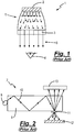
- It is known to employ LEDs within a spot light type system so as to provide an output that exhibits a narrow profile and which has a definable beam angle. An example of such a system is presented schematically in
Figure 1 , as represented generally byreference numeral 1. The LEDspot light system 1 can be seen to comprise a cluster ofLEDs 2 and alens structure 3 arranged such that it lies between the cluster ofLEDs 2 and anobserver 4. Typically, thelens structure 3 is placed at some distance from the cluster ofLEDs 2 so as to provide a means for collecting thelight 5 from all of the LEDs in thecluster 2 and projecting this light forward in a narrow and well definedbeam 6. The system is then orientated (or pointed) as a whole such that the narrowdefined beam 6 is delivered to a desired location. A disadvantage of this described configuration is that such systems tend to be large, bulky system that exhibit depths of many centimetres. - Another more recent approach to LED lighting is to couple the LEDs to light-guide plates. This is used to give a thin luminaire panel with a large area of diffuse lighting. Examples of such devices are provided by the inventor within
PCT Publication No. WO 2005/101070 and presented schematically inFigure 2 , as generally represented byreference numeral 7. Here alight source 8 is edge-coupled into aplanar light guide 9. Thelight 10 generated by thelight source 8 then propagates within the planar light-guide 9 due to the effects of total internal reflection. Extraction features 11 e.g. bumps, indents, grooves, ink dots or lines on the surface of theplanar light guide 9 then enable thelight 10 to escape the total internal reflection condition. Areflector 12 anddiffuser 13 may also be incorporated so as to provide a means for further manipulating thelight 10. The overall effect of this arrangement is that theplaner light guide 9 transforms the point sources of light, namely theLEDs 8, into a diffuse area of illumination. - Commercially available examples of such systems may typically comprise 600mm x 600mm sized panels that have LEDs located around the four edges of a sheet of a polymer light-guide plate. In practice it is found that as a result of the design of these systems the light output generated exhibits a very wide beam angle - typically lambertian (120° Full Width Half Maximum). These systems are well suited for many applications however their designs do exhibit a number of limitations which makes them unsuitable for other types of applications.
- In the first instance the optical coupling losses between the
LEDs 8 and the light-guide edge, in combination with the large average optical path lengths of thelight 10 within the absorbing transparent polymer of thepanel 9, results in a system that exhibits significant optical loss. This optical loss impacts on the overall optical efficiency of the systems which is known to be as low as 50%. - The most common polymer material employed as the transparent light-
guide plate 9 is acrylic (PMMA) due to this material having the highest optical transparency. However, compared with many other transparent materials (e.g. silicone), acrylic is not stable at high temperatures and high light power levels. Over time, the acrylic material is known to discolour and so light transmission is reduced. This is particularly evident in the areas closest to where theLEDs 8 are positioned, as they have the highest temperature and highest light power levels. These effects limit the working life-time of such products based on an acrylic light-guide. For lighting applications, where LEDs are promoted to have long life-times, this is a major disadvantage. - For applications where a particular beam angle distribution is required the wide, and usually lambertian, angular distribution of the output light provides further disadvantages. In such applications additional external films must be deployed, thus reducing further the optical efficiency, increasing production costs and providing general integration difficulties.
- Further examples representing the state of the art are described in
GB2474298 A GB2475738 A WO2007138294 A1 ,EP1867916 A1 , andGB2454928 A - It is therefore an object of an aspect of the present invention to obviate or at least mitigate the foregoing disadvantages of the LED based light source systems known in the art.
- A further aspect of an embodiment of the present invention is to provide an LED based lighting panel that exhibits a predetermined output beam angle.
- In the following description the terms transparent refers to the optical properties of a component of the lighting panel at the wavelengths of the light generated by the LED light sources employed within the apparatus.
- According to a first aspect of the present invention there is provided a lighting panel in accordance with
claim 1. - The lighting panels effectively provide an alternative means for producing a "spot light" like illumination from an LED. Having the LED embedded within the devices also provides the added advantage of significantly improving the optical coupling of the light into the guide layer while allowing the overall thickness of the device to be reduced. Embedding the LED source also provides them with physical protection while allowing for improved thermal dissipation. The lighting panels therefore exhibit high optical efficiencies and long operating lifetimes.
- The plurality of transparent prism structures extract the first and second light output from the lighting panel by disrupting internal reflection effects within the composite structure.
- Preferably the plurality of transparent prism structures are configured to compress the light emitted from the LED. In this context compression means that the width of the first and second light outputs is narrower than the width of the light emitted from the LED.
- Preferably the transparent coating is applied to the plurality of transparent prism structures so as to form a substantially planar surface. Having a substantially planar surface reduces the tendency for dirt or dust to settle on the exposed surface.
- Optionally, the transparent coating comprises a spatial pattern e.g. lined or chequered patterns. The spatial pattern acts to providing two components to both the first and second output beams. The resulting light intensity distribution is therefore a superposition of these two components of the first and second output beams.
- Optionally the lighting panel further comprises a reflector arranged so as to reflect the first light output back through the composite structure. In this embodiment the first light output is effectively combined with the second light output.
- The reflector may comprise an array of apertures. The array of apertures may be a regular array of apertures. The apertures may comprise a regular geometrical shape e.g. they may be circular.
- The reflector may comprise a transparent film and a plurality of patterned reflective or optical features. In this embodiment the reflector provides a means for controlling the proportion of light emitted within the first and second light outputs. It may also provide a means to further control the light beam profile and output angle of the first and second light outputs.
- Optionally the lighting panel further comprises a second LED mounted upon the second surface of the transparent substrate such that light emitted from second LED is guiding through the composite structure in a separate direction to that of the light emitted by the first LED. In this embodiment the configuration of the plurality of transparent prism structures acts to extract a third and a fourth light output from the lighting panel.
- Preferably the light emitted from second LED is guiding through the composite structure in an opposite direction to that of the light emitted by the first LED.
- The transparent substrate preferably has a refractive index ns between 1.50 and 1.66.
- The transparent prism structures preferably have a refractive index np between 1.46 and 1.58.
- The transparent guide layer preferably has a refractive index ng between 1.46 and 1.56.
- The transparent coating layer preferably has a refractive index nc between 1.37 and 1.58.
- Most preferably the refractive indices of the transparent substrate and the transparent prism structures are selected such that they satisfy the inequality ns ≥ np.
- Most preferably the refractive indices of the transparent substrate and the transparent guide layer are selected such that they satisfy the inequality ns ≥ ng.
- The refractive indices of the transparent prism structures and the transparent coating layer are selected such they satisfy the inequality np > nc.
- According to a second aspect of the present invention there is provided a method of producing a lighting panel in accordance with claim 11.
- Preferably the transparent coating is applied to the plurality of transparent prism structures so as to form a substantially planar surface.
- Optionally the method of producing a lighting panel further comprises arranging a reflector so as to reflect the first light output back through the composite structure.
- Optionally the method of producing a lighting panel further comprises mounting a second LED mounted upon the second surface of the transparent substrate such that light emitted from the second LED is guided through the composite structure in a separate direction to that of the light emitted by the first LED.
- Preferably the second LED is mounted upon the second surface of the transparent substrate such that light emitted from the second LED is guided through the composite structure in an opposite direction to that of the light emitted by the first LED.
- Embodiments of the second aspect of the invention may comprise features to implement the preferred or optional features of the first aspect of the invention or vice versa.
- Aspects and advantages of the present invention will become apparent upon reading the following detailed description and upon reference to the following drawings in which: The examples of
figures 3 ,5 ,6 and10 are not according to the invention and are present for illustration purposes only. -
Figure 1 presents a schematic representation of an LED spot light type system as known in the art; -
Figure 2 presents a side view of an LED based lighting panel as known in the art; -
Figure 3 presents a side view of a lighting panel in accordance with the disclosure; -
Figure 4 presents a beam profile measurement for the lighting panel ofFigure 3 . -
Figure 5 presents- (a) a side view of the lighting panel of
Figure 3 incorporating a reflective layer on the side of the prisms structures; and - (b) a top view of an alternative example of the reflector;
- (a) a side view of the lighting panel of
-
Figure 6 presents a side view of a lighting panel in accordance with an example; -
Figure 7 presents a representation of the light output of the lighting panel ofFigure 6 ; -
Figure 8 presents- (a) a side view of the lighting panel of
Figure 3 incorporating a coating on the prisms; - (b) A top view of an alternative embodiment of the coating;
- (a) a side view of the lighting panel of
-
Figure 9 presents a beam profile measurement taken from the lighting panels presented inFigure 3 andFigure 8 ; and -
Figure 10 presents a top view of a lighting panel in accordance with an alternative example of the present invention. - In the description which follows, like parts are marked throughout the specification and drawings with the same reference numerals. The drawings are not necessarily to scale and the proportions of certain parts have been exaggerated to better illustrate details and features of embodiments of the invention.
- Note that the examples of
figures 3 ,5 ,6 and10 are not according to the invention and are present for illustration purposes only. - Referring initially to
Figure 3 , a side view of alighting panel 14 in accordance with the disclosure is shown. Thelighting panel 14 can be seen to comprise asubstrate 15 made from a transparent polymer sheet, such as polyester or polycarbonate, and having a refractive index ns between 1.50 and 1.66. - Located on a
first surface 16 of thetransparent substrate 15, is an array of 90°prism structures 17, also formed from a transparent plastic polymer and having a refractive index np between 1.46 and 1.58. The refractive indices of thetransparent substrate 15 and thetransparent prism structures 17 are selected such that they satisfy the inequality ns ≥ np. - The
substrate 15 and theprism structures 17 can be provided as a single commercial product, a Vikuiti™ brightness enhancement film (BEF III) being an example of such a product employed within the presently described example. In this product the substrate has a thickness of approximately 127 microns while theprism structures 17 have a thickness of approximately 28 microns. The refractive index ns of thesubstrate 15 is selected to be 1.61 while the refractive index np of theprism structures 17 is chosen to be 1.58. - Located on a
second surface 18 of thesubstrate 15, thesecond surface 18 being opposite thefirst surface 16, is aside emitting LED 19 whose output has a lambertian distribution (120° full width half maximum), a Nichia® 206 LED being an example of a suitable LED device. Electrical tracking (not shown inFigure 3 ) is located on thesecond surface 18 of thesubstrate 15, and provides a means for supplying electrical power to theLED 19, as and when appropriate. The LEDs may be bonded to the tracks on thesecond surface 18 of thesubstrate 15 in a standard manner known to those in the art. - Covering the
LED 19 and the remaining area of thesecond surface 18 of thesubstrate 15 is aguide layer 20, also formed from a transparent plastic polymer, and having a refractive index ng between 1.46 and 1.56. The refractive indices of thetransparent substrate 15 and thetransparent guide layer 20 are selected such that they satisfy the inequality ns ≥ ng. In order to satisfy this inequality the presently described example employs atransparent guide layer 20 having a refractive index ng of 1.51. - As a result of the above arrangement and choice of the refractive indices ng, ns and np light 21 generated by the
LED 19 is initially coupled into thetransparent guide layer 20, so as to propagate in a direction substantially parallel to a plane defined by thetransparent substrate 15, as shown onFigure 3 . The light is however permitted to propagate into thetransparent substrate 15 and theprism structures 17, as is also shown inFigure 3 . - When the light 21 interacts with the
transparent prism structures 17, this acts to disrupt or overcome the effects of total internal reflection within the combined structure formed from between thetransparent guide layer 20 and thetransparent substrate 15. As a result, the light 21 is redirected so as to exit thelighting panel 14 via thetransparent prism structures 17, as a first light output as depicted byreference numeral 22, or via thetransparent guide layer 20, after propagating back through thetransparent substrate 15 and thetransparent guide layer 20, as a second light output as depicted byreference numeral 23. - It is the form of the prism structures that determines the output angles and beam widths of the first 22 and second 23 light outputs. Indeed the presence of the
prism structures 17 act to increase the on-axis brightness of the first 22 and second 23 light output beams by compressing the light into a narrower viewing angle. This compression of the light output beams 22 and 23 can clearly be seen within the transverse beam profile measurement (solid line) for thelighting panel 14 presented inFigure 4 . As can be seen, the firstlight output beam 22 has a beam distribution which peaks at approximately 60° from a normal to thetransparent substrate 15, has a full width half maximum of 30° and contains approximately 40% of the light exiting thedevice 14. By comparison, the secondlight output beam 23 has its peak at 25° from a normal to the exterior surface of theguide layer 20, exhibits a full width half maximum of 10° and contains approximately 60% of the light exiting the device. -
Figure 4 also presents an axial beam profile measurement (dashed line) of the light output beams 22 and 23 i.e. this is the view of the light output beams 22 and 23 as seen by theobserver 4. -
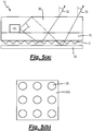
Figure 5(a) presents a side view of thelighting panel 14 ofFigure 3 , which now incorporates areflector 24 located such that thetransparent prism structures 17 lie between thereflective layer 24 and thetransparent substrate 15. The reflector may comprise a specular or non-specular reflective material. The inclusion of thereflector 24 acts to reflect thefirst light output 22 from thelighting panel 14 back through the device via theprism structures 17, such that this light 22 then contributes to the previously described secondlight output 23. - It will be appreciated by those skilled in the art that the
reflector 24 could be orientated on the opposite side of thelighting panel 14, to its position shown inFigure 5a . In this example, thereflector 24 acts to reflect thesecond light 23 output from thelighting panel 14, such that it passes back through the device, and then exits the device through theprism structures 17, so as to contribute to the previously described firstlight output 22. - A top view of an alternative reflector 24b is presented in
Figure 5(b) . The reflector 24b can be seen to comprise a 3x3 regular array ofcircular apertures 25 located across its surface area. The inclusion of these apertures provides a means for varying the proportion of light present within the light output beams 22 and 23 and on what side of the device they will be emitted. It will be appreciated by the skilled reader that the number, shape and alignment of the apertures can be altered. It is the combination of the size, number and relative arrangement of theapertures 25 which determine the proportion of light delivered outside the system on each side. - In a further example the
reflector 24 or 24b may comprise a transparent film with patterned reflective or optical features to control the proportion of light or further control the light beam profile and angle. In particular, locating the features on or around the LED positions can provide a means for reducing the glare or so-called "sparkle" as viewed by an observer. - A further example of the
lighting panel 14b is presented inFigure 6 . This example is similar to that presented inFigure 5 , however, instead of anLED 19 being located so as to propagate light in a single direction, asecond LED 26 is located on thefirst surface 16 of thesubstrate 15, such that light now propagates in both directions through thelighting panel 14b. In this example, instead of just thelight output 23 being generated by thelighting panel 14b, additionallight outputs light guide layer 20, and again exhibiting a full width half maximum of approximately 10°. - Further detail of the light output from the
lighting panel 14b ofFigure 6 is presented inFigure 7 . As can be clearly seen, this figure shows that with LEDs directing light in both directions, the light exiting system has twopeaks - The ability to further control the output beam angle of the light outputs 22, 23 and 27 from the
lighting panels Figure 8 . In particularFigure 8(a) presents a lighting panel 14c similar to that presented inFigure 3 , however in the presently described embodiment, atransparent coating layer 29 has been applied to the external surface of thetransparent prism structures 17. Thecoating layer 29 is again made from a transparent polymer, such as silicone, polyurethane or acrylic and has a refractive index nc between 1.37 and 1.47. The refractive indices of thetransparent prism structures 17 and thetransparent coating layer 29 are selected such they satisfy the inequality np > nc. As a result, and as shown inFigure 8(a) , light 21 generated by theLED 19 can propagate through the lighting panel 14c and into thecoating layer 29. In the presently described embodiment the refractive index of thecoating layer 29 is selected to be 1.42. - As a result of the introduction of the
coating layer 29, the beam angle of thefirst light output 22 from the lighting panel 14c is increased from 60° to 70° while that of the secondlight output 23 is increased from 25° to 50°. This effect is further illustrated by the beam profile measurement profile presented inFigure 9 , which shows the comparison of the secondlight output 23 from thelighting panel 14 and 14c presented inFigures 3 and8 . As can clearly be seen, the peak in the angle of distribution from the secondlight output 23 increases from 25° to 50°, as a result of the inclusion of thecoating layer 29. - It is preferable that the
coating layer 29 is added to theprism structures 17, so as to form a substantially planar surface. As a result, the secondlight output 23 is refracted by the combination of theprism structures 17 and thecoating layer 29, and not just thecoating layer 29 as may be expected to the non-informed observer. A further advantage of employing thecoating layer 29 to form a substantially planar surface, is that such a surface is less likely to collect dirt or dust when compared to that of theprism structures 17 in isolation. - As will be appreciated by the skilled reader, the refractive index of the
coating layer 29 can be selected so as to achieve the desired output angles for thebeams reflective layer 24, as previously discussed with reference toFigure 6 . In practice, it is found that patterning of thecoating layer 29 or controlling its depth can provide further control to the output angles for thebeams transparent coating layer 29b is presented inFigure 8(b) . The spatially pattern is a chequered square pattern which acts to providing two components to both the first 22 and second 23 output beams. The resulting light intensity distribution is therefore a superposition of these two components of the first 22 and second 23 output beams, thus providing a further method for determining the final profile and angle of the light beams. It will be appreciated by the skilled reader that other regular and irregular patters may be adopted by the patternedtransparent coating layer 29b e.g. lines or stripes. - In order to demonstrate the scalability of this device
Figure 10 presents a top view of acommercial lighting panel 14d in accordance with an example of the present invention. Thelighting panel 14d is based on a 300mm square section of a Vikuiti™ brightness enhancement film (BEF III) which performs the function of thetransparent substrate 15 and thetransparent prism structures 17. Located on thesecond surface 18 of thesubstrate 15 are one hundred and seventy six Nichia® 206LEDs 19. Electrical tracking 30 is located on thesecond surface 18 of thesubstrate 15, and provides a means for supplying electrical power to theLED 19, as and when appropriate. Theguide layer 20 again encapsulates theLEDs 19 on thesecond surface 18. Thelighting panel 14d has an overall thickness of around 2mm. - The above described embodiment and examples provide
lighting panels prism structures 17. - Furthermore, by embedding the
LEDs devices guide layer 20. This configuration also allows for theLEDs first surface 16 of thetransparent substrate 15 thus providing a means for significantly reducing the average optical path length of the light 21. The combination of both of these features results in systems that exhibit high optical efficiencies when compared to the lighting panel systems known in the art. - The described structures also have the further advantage in that they enable the use of more stable transparent optical polymers in the vicinity of the
LEDs lighting panels Figure 2 . Both of these features act in combination to provideLED lighting panels - The above embodiment and examples have all been described with reference to the employment of 90° prism 1-
dimensional structures 17. It will however be appreciated by the skilled reader that other angled prism structures could equally well be employed. Different output beam profiles and angle widths can also be obtained by employing different shaped prism structures, for example, lenses, micro-lenses, 2-dimensional prism pyramid structures or saw-tooth (asymmetric prisms), holographic and other diffractive or refractive structures. These can have a regular distribution or random distribution. - A further advantage of the above described
lighting panels angle light source LED sources lighting panels Figure 1 , would be required to produce the required focused beam and required optical efficiency. - In addition, the described
devices coating layer 29 onto the light extraction surface features17, which then function to modify the output beam angle of theoutput light layer 29 is selected to have a lower refractive index than the surface extraction features 17, but higher than that of air and so acts to increase the angle of distribution from the normal direction. The benefit of this approach is that it gives an easy manufacturing control of the output beam angles for a fixed substrate surface feature in the light panel structure. This avoids the costly requirement of producing a new light extracting feature design (prisms with different angles) for each required product beam angle. - A lighting panel that provide an alternative means for producing a "spot light" like illumination from an LED is described. The lighting panel comprising a transparent substrate upon a first surface of which are mounted a plurality of transparent prism structures and upon a second surface of which is mounted a light emitting diode (LED). A transparent guide layer is arranged so as to encapsulate the light emitting diode upon the second surface such that the transparent base substrate and the transparent guide light form a composite structure for guiding light emitted from the LED. The transparent prism structures are configured to extract a first and a second light output from the lighting panel, the first and second light outputs having output angles and beam widths determined by the structure of the plurality of transparent prism structures. The lighting panels exhibit high optical efficiencies and long operating lifetimes.
- The foregoing description of the invention has been presented for purposes of illustration and description and is not intended to be exhaustive or to limit the invention to the precise form disclosed. The described embodiments were chosen and described in order to best explain the principles of the invention and its practical application to thereby enable others skilled in the art to best utilise the invention in various embodiments and with various modifications as are suited to the particular use contemplated. Therefore, further modifications or improvements may be incorporated without departing from the scope of the invention as defined by the appended claims.
Claims (14)
- A lighting panel (14c) comprising a transparent substrate (15) upon a first surface (16) of which are mounted a plurality of transparent prism structures (17) and upon a second surface (18) of which is mounted a light emitting diode (LED) (19), and a transparent guide layer (20), the transparent guide layer (20) being arranged so as to encapsulate the LED (19) upon the second surface (18) such that the transparent substrate (15) and the transparent guide layer (20) form a composite structure for guiding light emitted from the LED (19), wherein the plurality of transparent prism structures (17) are configured to extract a first (22) and a second (23) light output from opposite sides of the lighting panel (14c), the first (22) and second (23) light outputs having output angles and beam widths determined by the plurality of transparent prism structures (17), wherein the lighting panel (14c) further comprises a transparent coating layer (29) applied to the plurality of transparent prism structures (17), wherein the first light output (22) exits the lighting panel (14c) through the transparent coating layer (29) where it is applied, wherein the refractive index of the transparent coating layer (29) is less than the refractive index of the transparent prism structures (17), and wherein the refractive index of the transparent coating layer (29) provides a further means for determining the output angles of the first (22) and second (23) light outputs.
- A lighting panel (14c) as claimed in claim 1 wherein the transparent coating layer (29) is applied to the plurality of transparent prism structures (17) to form a substantially planar surface.
- A lighting panel (14c) as claimed claim 1 or claim 2 wherein the transparent coating layer (29b) comprises a spatial pattern.
- A lighting panel (14c) as claimed in any of the preceding claims wherein the plurality of transparent prism structures (17) are configured to compress the light emitted from the LED (19).
- A lighting panel (14) as claimed in any of the preceding claims wherein the lighting panel further comprises a reflector (24) arranged so as to reflect the first light output (22) back through the composite structure.
- A lighting panel (14) as claimed in claim 5 wherein the reflector (24b) comprises an array of apertures (25).
- A lighting panel (14) as claimed in claim 5 or claim 6 wherein the reflector (24,24b) comprises a transparent film and a plurality of patterned reflective or optical features.
- A lighting panel (14b) as claimed in any of the preceding claims wherein the lighting panel (14b) further comprises a second LED (26) mounted upon the second surface (18) of the transparent substrate (15) such that light emitted from the second LED (26) is guided through the composite structure in a separate or opposite direction to that of the light emitted by the first LED (19).
- A lighting panel (14c) as claimed in any of the preceding claims wherein the transparent substrate (15) has a refractive index ns between 1.50 and 1.66, and/or wherein the transparent prism structures (17) have a refractive index np between 1.46 and 1.58, and/or wherein the transparent guide layer (20) has a refractive index ng between 1.46 and 1.56, and/or wherein the transparent coating layer (29) has a refractive index nc between 1.37 and 1.58.
- A lighting panel (14c) as claimed in claim 9 wherein the refractive indices of the transparent substrate (15) and the transparent prism structures (17) are selected such that they satisfy the inequality ns ≥ np, and/or wherein the refractive indices of the transparent substrate (15) and the transparent guide layer (20) are selected such that they satisfy the inequality ns ≥ ng.
- A method of producing a lighting panel (14c) the method comprising:- mounting a plurality of transparent prism structures (17) onto a first surface (16) of a transparent substrate (15);- mounting an LED (19) onto a second surface (18) of the transparent substrate (15);- adding a transparent guide layer (20) to the second surface (18) so as to encapsulate the LED (19) upon the second surface (18), such that the transparent substrate (15) and the transparent guide layer (20) form a composite structure for guiding light emitted from the LED (19);- configuring the mounted plurality of transparent prism structures (17) so as to extract a first (22) and a second (23) light output from opposite sides of the lighting panel (14c), the first (22) and second (23) light outputs having output angles and beam widths determined by the plurality of transparent prism structures (17), defined by:- applying a transparent coating layer (29) to the plurality of transparent prism structures (17), wherein the first light output (22) exits the lighting panel (14c) through the transparent coating layer (29) where it is applied, wherein the refractive index of the transparent coating layer (29) is less than the refractive index of the transparent prism structures (17), and wherein the refractive index of the transparent coating layer (29) provides a further means for determining the output angles of the first (22) and second (23) light outputs.
- A method of producing a lighting panel (14c) as claimed in claim 11 wherein the transparent coating layer (29) is applied to the plurality of transparent prism structures (17) to form a substantially planar surface.
- A method of producing a lighting panel (14) as claimed in claim 11 or claim 12 wherein the method further comprises arranging a reflector (24) so as to reflect the first light output (22) back through the composite structure.
- A method of producing a lighting panel (14b) as claimed in any of claims 11 to 13 wherein the method further comprises mounting a second LED upon the second surface of the transparent substrate such that light emitted from the second LED is guided through the composite structure in a separate or opposite direction to that of the light emitted by the first LED.
Applications Claiming Priority (2)
| Application Number | Priority Date | Filing Date | Title |
|---|---|---|---|
| GB1204167.9A GB2500055A (en) | 2012-03-09 | 2012-03-09 | Lighting panel with prisms and encapsulated light emitting diode |
| PCT/GB2013/050584 WO2013132271A1 (en) | 2012-03-09 | 2013-03-08 | Lighting panel |
Publications (2)
| Publication Number | Publication Date |
|---|---|
| EP2823221A1 EP2823221A1 (en) | 2015-01-14 |
| EP2823221B1 true EP2823221B1 (en) | 2021-02-24 |
Family
ID=46026266
Family Applications (1)
| Application Number | Title | Priority Date | Filing Date |
|---|---|---|---|
| EP13711730.5A Active EP2823221B1 (en) | 2012-03-09 | 2013-03-08 | Lighting panel and method of producing a lighting panel |
Country Status (5)
| Country | Link |
|---|---|
| US (1) | US20150043243A1 (en) |
| EP (1) | EP2823221B1 (en) |
| CN (1) | CN104145159A (en) |
| GB (1) | GB2500055A (en) |
| WO (1) | WO2013132271A1 (en) |
Families Citing this family (5)
| Publication number | Priority date | Publication date | Assignee | Title |
|---|---|---|---|---|
| CN203131706U (en) * | 2013-04-07 | 2013-08-14 | 京东方科技集团股份有限公司 | Light guide plate, backlight module and display device |
| GB2549801B (en) * | 2016-04-29 | 2018-08-29 | Design Led Products Ltd | Modular light panel |
| CN106125187A (en) * | 2016-06-24 | 2016-11-16 | 上海莹亮照明科技有限公司 | A kind of nano-micro structure optical system and preparation method thereof |
| DE102017113380A1 (en) | 2017-06-19 | 2018-12-20 | Schreiner Group Gmbh & Co. Kg | Film construction with generation of visible light by means of LED technology |
| DE102017113375A1 (en) | 2017-06-19 | 2018-12-20 | Schreiner Group Gmbh & Co. Kg | Film construction with generation of visible light by means of LED technology |
Citations (1)
| Publication number | Priority date | Publication date | Assignee | Title |
|---|---|---|---|---|
| GB2454928A (en) * | 2007-11-23 | 2009-05-27 | Iti Scotland Ltd | Light guides |
Family Cites Families (12)
| Publication number | Priority date | Publication date | Assignee | Title |
|---|---|---|---|---|
| JP3952923B2 (en) * | 2002-10-01 | 2007-08-01 | セイコーエプソン株式会社 | Manufacturing method of optical interconnection circuit |
| JP2004191392A (en) * | 2002-12-06 | 2004-07-08 | Seiko Epson Corp | Wavelength multiple intra-chip optical interconnection circuit, electro-optical device and electronic appliance |
| GB0408347D0 (en) | 2004-04-15 | 2004-05-19 | Design Led Products Ltd | Light guide device |
| JPWO2006107105A1 (en) * | 2005-04-01 | 2008-10-02 | ソニー株式会社 | Backlight device, liquid crystal display device, and light deflection sheet |
| GB2438440B (en) * | 2006-05-26 | 2008-04-23 | Design Led Products Ltd | A composite light guiding device |
| JP4528902B2 (en) * | 2008-08-06 | 2010-08-25 | 株式会社オプトデザイン | LIGHT SOURCE DEVICE, LIGHTING DEVICE, AND DISPLAY DEVICE |
| CN102282014B (en) * | 2008-11-19 | 2015-01-21 | 3M创新有限公司 | Reflective film combinations with output confinement in both polar and azimuthal directions and related constructions |
| GB2475738A (en) * | 2009-11-30 | 2011-06-01 | Iti Scotland Ltd | Light guide with heat sink |
| GB2474298A (en) * | 2009-10-12 | 2011-04-13 | Iti Scotland Ltd | Light Guide Device |
| JP5869494B2 (en) * | 2009-12-08 | 2016-02-24 | スリーエム イノベイティブ プロパティズ カンパニー | Optical structure incorporating light guide and low refractive index film |
| US20130063964A1 (en) * | 2010-05-12 | 2013-03-14 | Oree, Inc. | Illumination Apparatus with High Conversion Efficiency and Methods of Forming the Same |
| TWI410336B (en) * | 2010-07-13 | 2013-10-01 | Briview Corp | Decoration plate and an electronic device using the same |
-
2012
- 2012-03-09 GB GB1204167.9A patent/GB2500055A/en not_active Withdrawn
-
2013
- 2013-03-08 US US14/382,014 patent/US20150043243A1/en not_active Abandoned
- 2013-03-08 EP EP13711730.5A patent/EP2823221B1/en active Active
- 2013-03-08 CN CN201380012360.7A patent/CN104145159A/en active Pending
- 2013-03-08 WO PCT/GB2013/050584 patent/WO2013132271A1/en active Application Filing
Patent Citations (1)
| Publication number | Priority date | Publication date | Assignee | Title |
|---|---|---|---|---|
| GB2454928A (en) * | 2007-11-23 | 2009-05-27 | Iti Scotland Ltd | Light guides |
Also Published As
| Publication number | Publication date |
|---|---|
| WO2013132271A1 (en) | 2013-09-12 |
| GB201204167D0 (en) | 2012-04-25 |
| CN104145159A (en) | 2014-11-12 |
| US20150043243A1 (en) | 2015-02-12 |
| GB2500055A (en) | 2013-09-11 |
| EP2823221A1 (en) | 2015-01-14 |
Similar Documents
| Publication | Publication Date | Title |
|---|---|---|
| US11822113B2 (en) | Daylight responsive LED illumination panel with color temperature control | |
| US10422939B2 (en) | Waveguide having unidrectional illuminance | |
| US9612390B2 (en) | Diffractive luminaires | |
| US8827531B2 (en) | Lighting assembly | |
| US8789993B2 (en) | Light-emitting device | |
| EP3256776B1 (en) | White light source | |
| WO2012063759A1 (en) | Led lighting device | |
| EP2823221B1 (en) | Lighting panel and method of producing a lighting panel | |
| JP2015526863A (en) | Diffractive illumination device with a three-dimensional appearance | |
| TWI537527B (en) | Lighting device having a light guide structure | |
| EP2883094A1 (en) | Lighting devices with patterned printing of diffractive extraction features | |
| US20150160395A1 (en) | Light guide with light input features | |
| JP2012114081A (en) | Glare-reduced lighting system | |
| WO2012059866A1 (en) | Light emitting sheet | |
| WO2011148173A2 (en) | Lighting apparatus | |
| KR101684741B1 (en) | Back light unit | |
| JP6250269B2 (en) | Panel member and optical device | |
| KR101698004B1 (en) | See-through lighting window system | |
| WO2016003550A2 (en) | Waveguide having unidirectional illuminance | |
| EP2573458A1 (en) | Lighting device with uniformized luminous intensity | |
| WO2014096998A1 (en) | Illumination device and illumination system comprising an illumination device |
Legal Events
| Date | Code | Title | Description |
|---|---|---|---|
| PUAI | Public reference made under article 153(3) epc to a published international application that has entered the european phase |
Free format text: ORIGINAL CODE: 0009012 |
|
| 17P | Request for examination filed |
Effective date: 20140902 |
|
| AK | Designated contracting states |
Kind code of ref document: A1 Designated state(s): AL AT BE BG CH CY CZ DE DK EE ES FI FR GB GR HR HU IE IS IT LI LT LU LV MC MK MT NL NO PL PT RO RS SE SI SK SM TR |
|
| AX | Request for extension of the european patent |
Extension state: BA ME |
|
| DAX | Request for extension of the european patent (deleted) | ||
| STAA | Information on the status of an ep patent application or granted ep patent |
Free format text: STATUS: EXAMINATION IS IN PROGRESS |
|
| 17Q | First examination report despatched |
Effective date: 20180621 |
|
| GRAP | Despatch of communication of intention to grant a patent |
Free format text: ORIGINAL CODE: EPIDOSNIGR1 |
|
| STAA | Information on the status of an ep patent application or granted ep patent |
Free format text: STATUS: GRANT OF PATENT IS INTENDED |
|
| INTG | Intention to grant announced |
Effective date: 20200110 |
|
| GRAJ | Information related to disapproval of communication of intention to grant by the applicant or resumption of examination proceedings by the epo deleted |
Free format text: ORIGINAL CODE: EPIDOSDIGR1 |
|
| STAA | Information on the status of an ep patent application or granted ep patent |
Free format text: STATUS: EXAMINATION IS IN PROGRESS |
|
| INTC | Intention to grant announced (deleted) | ||
| GRAP | Despatch of communication of intention to grant a patent |
Free format text: ORIGINAL CODE: EPIDOSNIGR1 |
|
| STAA | Information on the status of an ep patent application or granted ep patent |
Free format text: STATUS: GRANT OF PATENT IS INTENDED |
|
| INTG | Intention to grant announced |
Effective date: 20200923 |
|
| GRAS | Grant fee paid |
Free format text: ORIGINAL CODE: EPIDOSNIGR3 |
|
| GRAA | (expected) grant |
Free format text: ORIGINAL CODE: 0009210 |
|
| STAA | Information on the status of an ep patent application or granted ep patent |
Free format text: STATUS: THE PATENT HAS BEEN GRANTED |
|
| AK | Designated contracting states |
Kind code of ref document: B1 Designated state(s): AL AT BE BG CH CY CZ DE DK EE ES FI FR GB GR HR HU IE IS IT LI LT LU LV MC MK MT NL NO PL PT RO RS SE SI SK SM TR |
|
| REG | Reference to a national code |
Ref country code: GB Ref legal event code: FG4D |
|
| REG | Reference to a national code |
Ref country code: CH Ref legal event code: EP |
|
| REG | Reference to a national code |
Ref country code: AT Ref legal event code: REF Ref document number: 1364907 Country of ref document: AT Kind code of ref document: T Effective date: 20210315 |
|
| REG | Reference to a national code |
Ref country code: IE Ref legal event code: FG4D |
|
| REG | Reference to a national code |
Ref country code: DE Ref legal event code: R096 Ref document number: 602013075837 Country of ref document: DE |
|
| REG | Reference to a national code |
Ref country code: LT Ref legal event code: MG9D |
|
| REG | Reference to a national code |
Ref country code: NL Ref legal event code: MP Effective date: 20210224 |
|
| PG25 | Lapsed in a contracting state [announced via postgrant information from national office to epo] |
Ref country code: LT Free format text: LAPSE BECAUSE OF FAILURE TO SUBMIT A TRANSLATION OF THE DESCRIPTION OR TO PAY THE FEE WITHIN THE PRESCRIBED TIME-LIMIT Effective date: 20210224 Ref country code: PT Free format text: LAPSE BECAUSE OF FAILURE TO SUBMIT A TRANSLATION OF THE DESCRIPTION OR TO PAY THE FEE WITHIN THE PRESCRIBED TIME-LIMIT Effective date: 20210624 Ref country code: HR Free format text: LAPSE BECAUSE OF FAILURE TO SUBMIT A TRANSLATION OF THE DESCRIPTION OR TO PAY THE FEE WITHIN THE PRESCRIBED TIME-LIMIT Effective date: 20210224 Ref country code: FI Free format text: LAPSE BECAUSE OF FAILURE TO SUBMIT A TRANSLATION OF THE DESCRIPTION OR TO PAY THE FEE WITHIN THE PRESCRIBED TIME-LIMIT Effective date: 20210224 Ref country code: GR Free format text: LAPSE BECAUSE OF FAILURE TO SUBMIT A TRANSLATION OF THE DESCRIPTION OR TO PAY THE FEE WITHIN THE PRESCRIBED TIME-LIMIT Effective date: 20210525 Ref country code: BG Free format text: LAPSE BECAUSE OF FAILURE TO SUBMIT A TRANSLATION OF THE DESCRIPTION OR TO PAY THE FEE WITHIN THE PRESCRIBED TIME-LIMIT Effective date: 20210524 Ref country code: NO Free format text: LAPSE BECAUSE OF FAILURE TO SUBMIT A TRANSLATION OF THE DESCRIPTION OR TO PAY THE FEE WITHIN THE PRESCRIBED TIME-LIMIT Effective date: 20210524 |
|
| REG | Reference to a national code |
Ref country code: AT Ref legal event code: MK05 Ref document number: 1364907 Country of ref document: AT Kind code of ref document: T Effective date: 20210224 |
|
| PG25 | Lapsed in a contracting state [announced via postgrant information from national office to epo] |
Ref country code: SE Free format text: LAPSE BECAUSE OF FAILURE TO SUBMIT A TRANSLATION OF THE DESCRIPTION OR TO PAY THE FEE WITHIN THE PRESCRIBED TIME-LIMIT Effective date: 20210224 Ref country code: PL Free format text: LAPSE BECAUSE OF FAILURE TO SUBMIT A TRANSLATION OF THE DESCRIPTION OR TO PAY THE FEE WITHIN THE PRESCRIBED TIME-LIMIT Effective date: 20210224 Ref country code: RS Free format text: LAPSE BECAUSE OF FAILURE TO SUBMIT A TRANSLATION OF THE DESCRIPTION OR TO PAY THE FEE WITHIN THE PRESCRIBED TIME-LIMIT Effective date: 20210224 Ref country code: NL Free format text: LAPSE BECAUSE OF FAILURE TO SUBMIT A TRANSLATION OF THE DESCRIPTION OR TO PAY THE FEE WITHIN THE PRESCRIBED TIME-LIMIT Effective date: 20210224 Ref country code: LV Free format text: LAPSE BECAUSE OF FAILURE TO SUBMIT A TRANSLATION OF THE DESCRIPTION OR TO PAY THE FEE WITHIN THE PRESCRIBED TIME-LIMIT Effective date: 20210224 |
|
| PG25 | Lapsed in a contracting state [announced via postgrant information from national office to epo] |
Ref country code: IS Free format text: LAPSE BECAUSE OF FAILURE TO SUBMIT A TRANSLATION OF THE DESCRIPTION OR TO PAY THE FEE WITHIN THE PRESCRIBED TIME-LIMIT Effective date: 20210624 |
|
| PG25 | Lapsed in a contracting state [announced via postgrant information from national office to epo] |
Ref country code: SM Free format text: LAPSE BECAUSE OF FAILURE TO SUBMIT A TRANSLATION OF THE DESCRIPTION OR TO PAY THE FEE WITHIN THE PRESCRIBED TIME-LIMIT Effective date: 20210224 Ref country code: AT Free format text: LAPSE BECAUSE OF FAILURE TO SUBMIT A TRANSLATION OF THE DESCRIPTION OR TO PAY THE FEE WITHIN THE PRESCRIBED TIME-LIMIT Effective date: 20210224 Ref country code: CZ Free format text: LAPSE BECAUSE OF FAILURE TO SUBMIT A TRANSLATION OF THE DESCRIPTION OR TO PAY THE FEE WITHIN THE PRESCRIBED TIME-LIMIT Effective date: 20210224 Ref country code: EE Free format text: LAPSE BECAUSE OF FAILURE TO SUBMIT A TRANSLATION OF THE DESCRIPTION OR TO PAY THE FEE WITHIN THE PRESCRIBED TIME-LIMIT Effective date: 20210224 |
|
| REG | Reference to a national code |
Ref country code: CH Ref legal event code: PL |
|
| REG | Reference to a national code |
Ref country code: DE Ref legal event code: R097 Ref document number: 602013075837 Country of ref document: DE |
|
| PG25 | Lapsed in a contracting state [announced via postgrant information from national office to epo] |
Ref country code: RO Free format text: LAPSE BECAUSE OF FAILURE TO SUBMIT A TRANSLATION OF THE DESCRIPTION OR TO PAY THE FEE WITHIN THE PRESCRIBED TIME-LIMIT Effective date: 20210224 Ref country code: SK Free format text: LAPSE BECAUSE OF FAILURE TO SUBMIT A TRANSLATION OF THE DESCRIPTION OR TO PAY THE FEE WITHIN THE PRESCRIBED TIME-LIMIT Effective date: 20210224 Ref country code: DK Free format text: LAPSE BECAUSE OF FAILURE TO SUBMIT A TRANSLATION OF THE DESCRIPTION OR TO PAY THE FEE WITHIN THE PRESCRIBED TIME-LIMIT Effective date: 20210224 Ref country code: ES Free format text: LAPSE BECAUSE OF FAILURE TO SUBMIT A TRANSLATION OF THE DESCRIPTION OR TO PAY THE FEE WITHIN THE PRESCRIBED TIME-LIMIT Effective date: 20210224 Ref country code: MC Free format text: LAPSE BECAUSE OF FAILURE TO SUBMIT A TRANSLATION OF THE DESCRIPTION OR TO PAY THE FEE WITHIN THE PRESCRIBED TIME-LIMIT Effective date: 20210224 |
|
| REG | Reference to a national code |
Ref country code: BE Ref legal event code: MM Effective date: 20210331 |
|
| PLBE | No opposition filed within time limit |
Free format text: ORIGINAL CODE: 0009261 |
|
| STAA | Information on the status of an ep patent application or granted ep patent |
Free format text: STATUS: NO OPPOSITION FILED WITHIN TIME LIMIT |
|
| PG25 | Lapsed in a contracting state [announced via postgrant information from national office to epo] |
Ref country code: IE Free format text: LAPSE BECAUSE OF NON-PAYMENT OF DUE FEES Effective date: 20210308 Ref country code: AL Free format text: LAPSE BECAUSE OF FAILURE TO SUBMIT A TRANSLATION OF THE DESCRIPTION OR TO PAY THE FEE WITHIN THE PRESCRIBED TIME-LIMIT Effective date: 20210224 Ref country code: CH Free format text: LAPSE BECAUSE OF NON-PAYMENT OF DUE FEES Effective date: 20210331 Ref country code: LI Free format text: LAPSE BECAUSE OF NON-PAYMENT OF DUE FEES Effective date: 20210331 Ref country code: LU Free format text: LAPSE BECAUSE OF NON-PAYMENT OF DUE FEES Effective date: 20210308 |
|
| 26N | No opposition filed |
Effective date: 20211125 |
|
| PG25 | Lapsed in a contracting state [announced via postgrant information from national office to epo] |
Ref country code: SI Free format text: LAPSE BECAUSE OF FAILURE TO SUBMIT A TRANSLATION OF THE DESCRIPTION OR TO PAY THE FEE WITHIN THE PRESCRIBED TIME-LIMIT Effective date: 20210224 |
|
| PG25 | Lapsed in a contracting state [announced via postgrant information from national office to epo] |
Ref country code: IT Free format text: LAPSE BECAUSE OF FAILURE TO SUBMIT A TRANSLATION OF THE DESCRIPTION OR TO PAY THE FEE WITHIN THE PRESCRIBED TIME-LIMIT Effective date: 20210224 |
|
| PG25 | Lapsed in a contracting state [announced via postgrant information from national office to epo] |
Ref country code: IS Free format text: LAPSE BECAUSE OF FAILURE TO SUBMIT A TRANSLATION OF THE DESCRIPTION OR TO PAY THE FEE WITHIN THE PRESCRIBED TIME-LIMIT Effective date: 20210624 |
|
| PG25 | Lapsed in a contracting state [announced via postgrant information from national office to epo] |
Ref country code: BE Free format text: LAPSE BECAUSE OF NON-PAYMENT OF DUE FEES Effective date: 20210331 |
|
| PGFP | Annual fee paid to national office [announced via postgrant information from national office to epo] |
Ref country code: FR Payment date: 20230222 Year of fee payment: 11 |
|
| PG25 | Lapsed in a contracting state [announced via postgrant information from national office to epo] |
Ref country code: HU Free format text: LAPSE BECAUSE OF FAILURE TO SUBMIT A TRANSLATION OF THE DESCRIPTION OR TO PAY THE FEE WITHIN THE PRESCRIBED TIME-LIMIT; INVALID AB INITIO Effective date: 20130308 |
|
| PGFP | Annual fee paid to national office [announced via postgrant information from national office to epo] |
Ref country code: GB Payment date: 20230222 Year of fee payment: 11 Ref country code: DE Payment date: 20230221 Year of fee payment: 11 |
|
| PG25 | Lapsed in a contracting state [announced via postgrant information from national office to epo] |
Ref country code: CY Free format text: LAPSE BECAUSE OF FAILURE TO SUBMIT A TRANSLATION OF THE DESCRIPTION OR TO PAY THE FEE WITHIN THE PRESCRIBED TIME-LIMIT Effective date: 20210224 |