EP2821849A1 - Image projection apparatus and circuit-board retaining structure - Google Patents
Image projection apparatus and circuit-board retaining structure Download PDFInfo
- Publication number
- EP2821849A1 EP2821849A1 EP14170077.3A EP14170077A EP2821849A1 EP 2821849 A1 EP2821849 A1 EP 2821849A1 EP 14170077 A EP14170077 A EP 14170077A EP 2821849 A1 EP2821849 A1 EP 2821849A1
- Authority
- EP
- European Patent Office
- Prior art keywords
- circuit board
- image
- connector
- retaining member
- projection apparatus
- Prior art date
- Legal status (The legal status is an assumption and is not a legal conclusion. Google has not performed a legal analysis and makes no representation as to the accuracy of the status listed.)
- Granted
Links
Images







Classifications
-
- H—ELECTRICITY
- H04—ELECTRIC COMMUNICATION TECHNIQUE
- H04N—PICTORIAL COMMUNICATION, e.g. TELEVISION
- H04N5/00—Details of television systems
- H04N5/74—Projection arrangements for image reproduction, e.g. using eidophor
- H04N5/7475—Constructional details of television projection apparatus
-
- H—ELECTRICITY
- H04—ELECTRIC COMMUNICATION TECHNIQUE
- H04N—PICTORIAL COMMUNICATION, e.g. TELEVISION
- H04N5/00—Details of television systems
- H04N5/74—Projection arrangements for image reproduction, e.g. using eidophor
- H04N5/7416—Projection arrangements for image reproduction, e.g. using eidophor involving the use of a spatial light modulator, e.g. a light valve, controlled by a video signal
- H04N5/7458—Projection arrangements for image reproduction, e.g. using eidophor involving the use of a spatial light modulator, e.g. a light valve, controlled by a video signal the modulator being an array of deformable mirrors, e.g. digital micromirror device [DMD]
-
- G—PHYSICS
- G03—PHOTOGRAPHY; CINEMATOGRAPHY; ANALOGOUS TECHNIQUES USING WAVES OTHER THAN OPTICAL WAVES; ELECTROGRAPHY; HOLOGRAPHY
- G03B—APPARATUS OR ARRANGEMENTS FOR TAKING PHOTOGRAPHS OR FOR PROJECTING OR VIEWING THEM; APPARATUS OR ARRANGEMENTS EMPLOYING ANALOGOUS TECHNIQUES USING WAVES OTHER THAN OPTICAL WAVES; ACCESSORIES THEREFOR
- G03B21/00—Projectors or projection-type viewers; Accessories therefor
- G03B21/14—Details
-
- G—PHYSICS
- G03—PHOTOGRAPHY; CINEMATOGRAPHY; ANALOGOUS TECHNIQUES USING WAVES OTHER THAN OPTICAL WAVES; ELECTROGRAPHY; HOLOGRAPHY
- G03B—APPARATUS OR ARRANGEMENTS FOR TAKING PHOTOGRAPHS OR FOR PROJECTING OR VIEWING THEM; APPARATUS OR ARRANGEMENTS EMPLOYING ANALOGOUS TECHNIQUES USING WAVES OTHER THAN OPTICAL WAVES; ACCESSORIES THEREFOR
- G03B21/00—Projectors or projection-type viewers; Accessories therefor
- G03B21/14—Details
- G03B21/145—Housing details, e.g. position adjustments thereof
-
- G—PHYSICS
- G03—PHOTOGRAPHY; CINEMATOGRAPHY; ANALOGOUS TECHNIQUES USING WAVES OTHER THAN OPTICAL WAVES; ELECTROGRAPHY; HOLOGRAPHY
- G03B—APPARATUS OR ARRANGEMENTS FOR TAKING PHOTOGRAPHS OR FOR PROJECTING OR VIEWING THEM; APPARATUS OR ARRANGEMENTS EMPLOYING ANALOGOUS TECHNIQUES USING WAVES OTHER THAN OPTICAL WAVES; ACCESSORIES THEREFOR
- G03B21/00—Projectors or projection-type viewers; Accessories therefor
- G03B21/14—Details
- G03B21/147—Optical correction of image distortions, e.g. keystone
-
- H—ELECTRICITY
- H04—ELECTRIC COMMUNICATION TECHNIQUE
- H04N—PICTORIAL COMMUNICATION, e.g. TELEVISION
- H04N9/00—Details of colour television systems
- H04N9/12—Picture reproducers
- H04N9/31—Projection devices for colour picture display, e.g. using electronic spatial light modulators [ESLM]
- H04N9/3102—Projection devices for colour picture display, e.g. using electronic spatial light modulators [ESLM] using two-dimensional electronic spatial light modulators
- H04N9/3111—Projection devices for colour picture display, e.g. using electronic spatial light modulators [ESLM] using two-dimensional electronic spatial light modulators for displaying the colours sequentially, e.g. by using sequentially activated light sources
- H04N9/3114—Projection devices for colour picture display, e.g. using electronic spatial light modulators [ESLM] using two-dimensional electronic spatial light modulators for displaying the colours sequentially, e.g. by using sequentially activated light sources by using a sequential colour filter producing one colour at a time
-
- H—ELECTRICITY
- H04—ELECTRIC COMMUNICATION TECHNIQUE
- H04N—PICTORIAL COMMUNICATION, e.g. TELEVISION
- H04N9/00—Details of colour television systems
- H04N9/12—Picture reproducers
- H04N9/31—Projection devices for colour picture display, e.g. using electronic spatial light modulators [ESLM]
- H04N9/3141—Constructional details thereof
-
- G—PHYSICS
- G03—PHOTOGRAPHY; CINEMATOGRAPHY; ANALOGOUS TECHNIQUES USING WAVES OTHER THAN OPTICAL WAVES; ELECTROGRAPHY; HOLOGRAPHY
- G03B—APPARATUS OR ARRANGEMENTS FOR TAKING PHOTOGRAPHS OR FOR PROJECTING OR VIEWING THEM; APPARATUS OR ARRANGEMENTS EMPLOYING ANALOGOUS TECHNIQUES USING WAVES OTHER THAN OPTICAL WAVES; ACCESSORIES THEREFOR
- G03B21/00—Projectors or projection-type viewers; Accessories therefor
- G03B21/14—Details
- G03B21/28—Reflectors in projection beam
Definitions
- the present invention relates generally to image projection apparatuses and circuit-board retaining structures.
- Some types of image projection apparatuses project an image onto a projection surface such as a screen by directing light from a light source to an image display device, such as a liquid crystal panel or a digital micro-mirror device (DMD), and projecting light modulated by the image display device according to the image onto the projection surface.
- an image projection apparatus includes at least a circuit board on which an image display device mounted and a control circuit board configured to control the image display device and the like. These circuit boards are electrically connected to each other via a connector.
- This type of image projection apparatus typically has the following configuration: a DMD circuit board including the image display device is positioned horizontally; and a main circuit board which controls the image projection apparatus is positioned vertically and connected to the DMD circuit board via a connector. If electrical noise is undesirably generated at a portion near the connector, a shield structure will be added to the image projection apparatus to prevent external leakage of the noise. As a result, even though the volume size of the image projection apparatus can be reduced by virtue of the optical system configuration described above, addition of the shield structure increases the apparatus in size.
- Japanese Laid-open Patent Publication No. 02-161798 discloses a structure for reducing noise of a main circuit board and a sub circuit board connected to each other via a connector.
- the main circuit board and the sub circuit board are arranged parallel to each other and each of the circuit boards is ground connected to a chassis interposed therebetween.
- an image display device such as a DMD and other circuit boards are typically arranged perpendicular to each other.
- an image projection apparatus for projecting an image onto a projection surface
- the image projection apparatus comprising: a light source device configured to emit light; a first circuit board including an image display device configured to form an image using the light, a connector, and an electrically conductive portion near the connector; a retaining member made of metal; an optical illuminating unit held by the retaining member and configured to guide the light emitted from the light source device to the image display device; an optical projecting unit configured to project the image formed by the image display device onto the projection surface; a second circuit board configured to be electrically connected to the connector of the first circuit board; a metal plate fixed and electrically connected to the retaining member; and an elastic metal member arranged on the metal plate, wherein the first circuit board is fixed to the retaining member, the elastic metal member is in contact with the electrically conductive portion of the first circuit board, and the second circuit board is fixed and electrically connected to the metal plate.
- the present invention also provides a circuit-board retaining structure comprising: a first circuit board (42) including an image display device (41) configured to form an image using light, a connector (42a), and an electrically conductive portion (45, 46) near the connector (42a); a retaining member (56) made of metal; a second circuit board (80) configured to be electrically connected to the connector (42a) of the first circuit board (42); a metal plate (70) fixed and electrically connected to the retaining member (56); and an elastic metal member (73, 74) arranged on the metal plate (70), wherein the first circuit board (42) is fixed to the retaining member (56), the elastic metal member (73, 74) is in contact with the electrically conductive portion (45, 46) of the first circuit board (42), and the second circuit board (80) is fixed and electrically connected to the metal plate (70).
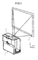
- FIG. 1 is an exterior perspective view of an image projection apparatus 1 according to an embodiment of the present invention.
- the image projection apparatus 1 forms an image based on image data fed from a personal computer, a video camera, or the like, and projects and displays the image onto a screen 2.
- Examples of the image projection apparatus 1 include liquid crystal projectors which are widely known. Liquid crystal projectors have become improved in brightness and less expensive by virtue of recent efficiency enhancement of light source lamps.
- Compact and lightweight image projection apparatuses with digital micro-mirror devices (DMDs) are proliferating not only in offices and schools but also for home use. In particular, front projectors which are improved in portability are coming into extensive use, including in small meetings of several members.
- DMDs digital micro-mirror devices
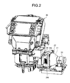
- FIG. 2 is a perspective view of the image projection apparatus 1 illustrated in FIG. 1 with an outer casing 3 removed.
- the image projection apparatus 1 primarily includes an optical engine unit 30 and a light source device 20.
- the light source device 20 supplies white light necessary for image projection to the optical engine unit 30 by controlling a light source such as a high-pressure mercury lamp.
- the light source device 20 includes a light source bracket 22 as a holding member which supports a light source 21 such as a halogen lamp, a metal halide lamp, or a high-pressure mercury lamp.
- the light source 21 is mounted at an upper portion of the light source bracket 22.
- a holder 24, which holds a reflector and the like (not shown), is screwed into the light source bracket 22 on a side from which light from the light source 21 exits.
- the holder 24 has, on the side opposite from the light source 21, an exit window 23 (see FIG. 3 ). The light exiting from the light source 21 is converged to the exit window 23 by the reflector (not shown) and goes out through the exit window 23.
- the holder 24 further has, on its side surface, a light-source air-inlet opening 24b, through which air for cooling the light source 21 is to flow in.
- the holder 24 further has, on its top surface, a light-source air-outlet opening 24c, through which air heated by the light source 21 is to exit.
- the optical engine unit 30 provides control of processing light supplied from the light source device 20 according to input image data and projecting the processed light.
- FIG. 3 is a schematic perspective view illustrating a configuration of the optical engine unit 30 in detail.
- the optical engine unit 30 includes an optical illuminating unit 31, and optical projecting unit 33, and an image processing unit 32.
- the white light from the light source device 20 described above is directed to the optical illuminating unit 31.
- the optical illuminating unit 31 separates the white light emitted from the light source device 20 into red, green, and blue (RGB) components, and guides the components to the image processing unit 32.
- the image processing unit 32 forms an image according to modulation signals.
- the optical projecting unit 33 projects and magnifies the image formed by the image processing unit 32.
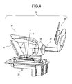
- FIG. 4 is a diagram illustrating a layout of the optical illuminating unit 31 and the image processing unit 32.
- the optical illuminating unit 31 includes a color wheel 38, a light tunnel 37, a relay lens 36, a cylindrical mirror 35, and a concave mirror 34.
- the color wheel 38 which includes a disc-like color filter, converts the white light emitted from the light source device 20 into light of one of R, G, and B every unit time using the color filter and emits the converted light.
- the light tunnel 37 is formed by joining plate glasses together into a cylindrical shape.
- the light tunnel 6 guides the light exiting from the color wheel 38 to the relay lens 36.
- the relay lens 36 is formed by combining two lenses and converges the light exiting from the light tunnel 37 while correcting axial chromatic aberration.
- the cylindrical mirror 35 and the concave mirror 34 reflect the light exiting from the relay lens 36.
- the reflected light enters the image processing unit 32.
- the image processing unit 32 includes a DMD (an example of an image display device) 41 (see FIG. 5 ) which includes a substantially-rectangular mirror surface made up of a plurality of micromirrors.
- the DMD 41 processes and reflects projection light so as to form a desired image by driving (i.e., repositioning) the micromirrors individually in a time-division manner according to image data.
- light for use by the plurality of micromirrors of the DMD 41 in the time-division manner according to the image data is reflected toward a projector lens 51 in a direction indicated by arrow B in FIG. 4 , while unnecessary light is reflected toward a light sink in a direction indicated by arrow C.
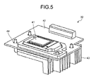
- FIG. 5 is a perspective view illustrating a configuration of the image processing unit 32.
- the image processing unit 32 includes the DMD 41, a DMD printed circuit board (hereinafter, "DMD PCB") 42 (first circuit board) which controls the DMD 41, a heat sink 43 which cools the DMD 41, and a fixing plate 44 which presses the heat sink 43 against the DMD 41.
- the heat sink 43 serves as a heat dissipating unit.
- the heat sink 43 is brought into contact with the to-be-cooled DMD 41 to thereby dissipate heat emitted from the DMD 41.
- FIG. 6 is a perspective view illustrating a configuration of the optical projecting unit 33 in detail.
- the light exiting from the image processing unit 32 is reflected toward the projector lens 51 illustrated in FIG. 7 .
- the unnecessary light is reflected toward the light sink 53 illustrated in FIG. 7 .
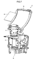
- FIG. 7 and FIG. 8 are a perspective view and a side view, respectively, illustrating the configuration of the optical projecting unit 33.
- Magnified image light exiting from the projector lens 51 travels along an optical path which is folded by a folding mirror 54. The light is then reflected off a free-form mirror 55 to project and magnify the image on the screen 2. Because the configuration described above allows placing the optical engine unit 30 in proximity to the screen 2, the image projection apparatus 1 can be designed to have a compact, upright structure, in which elements are vertically stacked, requiring a smaller footprint.
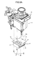
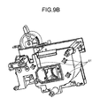
- FIGS. 9A and 9B are diagrams illustrating a method for assembling the image processing unit 32 onto the optical illuminating unit 31.
- the DMD PCB 42 including the DMD 41 is fastened in a horizontal orientation to the optical illuminating unit 31 by inserting screws 61 into holes 47 at four positions near the DMD 41 with the DMD 41 at substantially their center.
- the reason for adopting this assembly method is as follows.
- the DMD 41 is one of main optical elements and therefore positional accuracy of the DMD 41 with respect to the optical illuminating unit 31 matters considerably.
- the configuration of screwing the DMD 41 at the four positions near the DMD 41 with the DMD 41 at substantially their center is functionally favorable.
- a large portion of electrical noise originates near a connector 42a for connection with a control circuit board (second circuit board) 80 (see FIGS. 14A and 14B ), which will be described later, rather than near the DMD 41.
- FIGS. 10 and 11 are diagrams describing a method for providing electrical ground connection to the DMD PCB 42.
- a metal earth plate 70 is fixed to the optical illuminating unit 31 in a fashion illustrated in FIGS. 10 and 11 .
- Metal leaf spring members 74 and 73 which are elastic members made of metal, are fixed to the metal earth plate 70.
- the metal leaf-spring members 74 and 73 differ from each other in urged direction.
- the metal leaf-spring member 73 is urged upward in FIG. 11
- the metal leaf-spring member 74 is urged downward in FIG. 11 .
- the metal leaf-spring member 74 is placed on a back side of the DMD PCB 42 at a position near the connector 42a.
- the metal leaf-spring member 74 contacts a conductive portion 45 of the DMD PCB 42 where a resist (insulating) layer is stripped off, thereby making electrical ground connection between the metal earth plate 70 and the DMD PCB 42.
- the metal leaf-spring member 73 is on a front side of the DMD PCB 42 at a position near the connector 42a.
- the metal leaf-spring member 73 contacts a conductive portion 46 of the DMD PCB 42 where the resist (insulating) layer is stripped off, thereby making electrical ground connection between the metal earth plate 70 and the DMD PCB 42.
- the conductive portion 46 is positioned on the DMD PCB 42 to be closer to the connector 42a than the positions where the DMD PCB 42 is fixed to the optical illuminating unit 31.
- the elastic members are not limited to those of this embodiment. Any elastic members having elasticity and configured to be brought into contact with the conductive portions 45 and46 can be employed.
- FIG. 12A and FIG. 12B are diagrams illustrating the metal leaf-spring member 74 and the conductive portion 46 in contact with each other and the metal leaf-spring member 73 and the conductive portion 45 in contact with each other, respectively.
- the metal earth plate 70 is fastened to a metal member (made of Mg alloy) 56 of the optical illuminating unit 31 with a screw 75 and a screw 76.
- the metal member 56 is a retaining member such as a bracket which supports components of the optical illuminating unit 31.
- the metal leaf-spring members 74 and 73 are fixed to the metal earth plate 70 at different positions.
- One of the metal leaf-spring members 74 and 73 is in contact with the conductive portion 46 at the position near the connector 42a on the front face of the DMD PCB 42.
- the other one of the metal leaf-spring members 74 and 73 is in contact with the conductive portion 45 at the position near the connector 42a on the back face of the DMD PCB 42.
- the shapes of the metal leaf-spring members 74 and 73 are not limited to those of this embodiment.
- the metal leaf-spring members 74 and 73 may be configured to have two or more projections tops of which are to be brought into contact with the conductive portion 45 or 46 so that a contact area can be increased.
- each of the metal leaf-spring members 74 and 73 is fixed to the metal earth plate 70 by being crimped at a flange.
- the metal leaf-spring members 74 and 73 arranged at the different, or two, positions are identical components which are fixed with one of them in an upside-down orientation. Adopting such configuration of the metal leaf-spring members 74 and 73 allows cost saving by not increasing variety of dies.
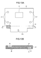
- FIGS. 13A and 13B illustrate a configuration of the DMD PCB 42 including the DMD 41.
- the DMD PCB 42 has a four-layer structure, in which each of the entire first layer and the entire fourth layer is covered with a resist (insulating) layer 49.
- a ground layer 50 is laid on an inner side of the resist layers 49.
- the resist layers 49 are stripped off to expose the ground layer 50 at the conductive portions 45 and 46.
- Pattern layers 48 are laid between the resist layers 49 and the ground layer 50.
- FIGS. 14A and 14B are diagrams illustrating a method for assembling a control circuit board 80 to the DMD PCB 42 with connector-connecting.
- the control circuit board 80 is connected to the DMD PCB 42 by connecting a connector 82 to the connector 42a.
- the control circuit board 80 is fastened to the metal earth plate 70 at two fixation positions near the connector 82 with screws 81.
- FIGS. 15A and 15B illustrate a configuration of a front side and that of a back side, respectively, of the control circuit board 80.
- the control circuit board 80 includes conductive portions 83 on the front side and conductive portions 84 and the back side formed by stripping off resist (insulating) layers at the fixation positions where the control circuit board 80 is fastened to the DMD PCB 42 with the screws 81.
- Ground connection to the metal earth plate 70 is made at the fixation positions.
- each of the DMD PCB 42 and the control circuit board 80 is ground connected to the metal earth plate 70, which includes the metal leaf-spring members 73 and 74, on each of the front side and the back side of the circuit board at the positions near the connector of the circuit board. Accordingly, electrical noise can be reduced efficiently.
- FIGS. 16 and 17 are diagrams illustrating how other members are assembled onto the control circuit board 80 in detail.
- Insertion-type input/output terminal(s) e.g., an HDMI (registered trademark) connector and an RGB connector, for use in external input and output are mounted on the control circuit board 80.
- an HDMI (registered trademark) connector and an RGB connector for use in external input and output are mounted on the control circuit board 80.
- an insertion or withdrawal force is applied to the input/output terminal.
- control circuit board 80 Because the control circuit board 80 is fixed to the DMD PCB 42 on which the DMD 41 is mounted and to the optical illuminating unit 31, this force can be applied to the connector 82, with which the control circuit board 80 is connected to the DMD PCB 42, and the optical illuminating unit 31, causing a damage to or contact failure at the connector 82 to occur. Resultant adverse effects such as an increase in electrical noise, and degradation in positional accuracy of optical elements including the lenses and the mirrors in the optical illuminating unit 31 and positional accuracy of the DMD 41 can lead to a problem such as image deformation.
- a screw hole is defined in the input/output terminal, e.g., the HDMI (registered trademark) connector and the RGB connector, and the input/output terminal is fastened to a PCB bracket 90 (second retaining member) with a screw.
- This structure causes all force which is applied due to externally insertion or withdrawal of a cable terminal to and from the connector to be received by the PCB bracket 90. Because the PCB bracket 90 is fixed to a housing or the like of the image projection apparatus 1 but not fixed to the optical illuminating unit 31, the insertion or withdrawal force is prevented from being applied to optical elements where positional accuracy is required and the connector.
- the image projection apparatus 1 is configured as follows.
- the DMD PCB 42 and the control circuit board 80 are ground connected to the metal earth plate 70 at the positions near connectors 42a and 82 where a large portion of electrical noise originates.
- the metal earth plate 70 is connected to the metal member, which has largest capacitance, of the optical illuminating unit 31. Accordingly, because electrical noise can be reduced efficiently, an increase in size of the image projection apparatus 1 can be reduced.
- an image projection apparatus generates less electrical noise than conventional image projection apparatuses.
Landscapes
- Engineering & Computer Science (AREA)
- Multimedia (AREA)
- Signal Processing (AREA)
- Physics & Mathematics (AREA)
- General Physics & Mathematics (AREA)
- Projection Apparatus (AREA)
- Transforming Electric Information Into Light Information (AREA)
- Microelectronics & Electronic Packaging (AREA)
Abstract
Description
- The present invention relates generally to image projection apparatuses and circuit-board retaining structures.
- Some types of image projection apparatuses project an image onto a projection surface such as a screen by directing light from a light source to an image display device, such as a liquid crystal panel or a digital micro-mirror device (DMD), and projecting light modulated by the image display device according to the image onto the projection surface. To perform image projection in this manner, such an image projection apparatus includes at least a circuit board on which an image display device mounted and a control circuit board configured to control the image display device and the like. These circuit boards are electrically connected to each other via a connector.
- There is a demand for projectors as image projection apparatuses to accomplish projecting a large screen image while minimizing projection space required outside the projector. To increase a projection screen size while reducing projection space outside an image projection apparatus, it is desirable to place as large a portion of an optical path of imaging light which forms an image to be projected as possible inside the projector. An image projection apparatus including such an optical system is disclosed in Japanese Patent No.
4210314 - Japanese Laid-open Patent Publication No.
02-161798 - However, an image display device such as a DMD and other circuit boards are typically arranged perpendicular to each other.
- In view of the above circumstances, there is a need to provide an image projection apparatus which generates less electrical noise than conventional image projection apparatuses.
- It is an object of the present invention to at least partially solve the problem in the conventional technology.
- It is an object of the present invention to at least partially solve the problems in the conventional technology.
- According to the present invention, there is provided an image projection apparatus for projecting an image onto a projection surface, the image projection apparatus comprising: a light source device configured to emit light; a first circuit board including an image display device configured to form an image using the light, a connector, and an electrically conductive portion near the connector; a retaining member made of metal; an optical illuminating unit held by the retaining member and configured to guide the light emitted from the light source device to the image display device; an optical projecting unit configured to project the image formed by the image display device onto the projection surface; a second circuit board configured to be electrically connected to the connector of the first circuit board; a metal plate fixed and electrically connected to the retaining member; and an elastic metal member arranged on the metal plate, wherein the first circuit board is fixed to the retaining member, the elastic metal member is in contact with the electrically conductive portion of the first circuit board, and the second circuit board is fixed and electrically connected to the metal plate.
- The present invention also provides a circuit-board retaining structure comprising: a first circuit board (42) including an image display device (41) configured to form an image using light, a connector (42a), and an electrically conductive portion (45, 46) near the connector (42a); a retaining member (56) made of metal; a second circuit board (80) configured to be electrically connected to the connector (42a) of the first circuit board (42); a metal plate (70) fixed and electrically connected to the retaining member (56); and an elastic metal member (73, 74) arranged on the metal plate (70), wherein the first circuit board (42) is fixed to the retaining member (56), the elastic metal member (73, 74) is in contact with the electrically conductive portion (45, 46) of the first circuit board (42), and the second circuit board (80) is fixed and electrically connected to the metal plate (70).
- The above and other objects, features, advantages and technical and industrial significance of this invention will be better understood by reading the following detailed description of presently preferred embodiments of the invention, when considered in connection with the accompanying drawings.
-
FIG. 1 is a perspective view illustrating a use situation of an image projection apparatus according to a first embodiment of the present invention; -
FIG. 2 is a perspective view of an optical engine unit and a light source device of the image projection apparatus shown inFIG. 1 ; -
FIG. 3 is a perspective view of the optical engine unit of the image projection apparatus; -
FIG. 4 is a perspective view of an optical illuminating unit and an image processing unit of the image projection apparatus; -
FIG. 5 is a perspective view of the image processing unit of the image projection apparatus; -
FIG. 6 is a perspective view of an optical projecting unit of the image projection apparatus; -
FIG. 7 is a perspective view of the optical projecting unit of the image projection apparatus; -
FIG. 8 is a side view of the optical projecting unit of the image projection apparatus; -
FIG. 9A is a diagram illustrating a method for assembling the image processing unit onto the optical illuminating unit of the image projection apparatus; -
FIG. 9B is another diagram illustrating the method for assembling the image processing unit onto the optical illuminating unit of the image projection apparatus; -
FIG. 10 is a diagram illustrating a method for providing electrical ground connection to a DMD Print Circuit Board (PCB); -
FIG. 11 is another diagram illustrating the method for providing electrical ground connection to the DMD PCB; -
FIG. 12A is a diagram illustrating a metal leaf-spring member and a conductive portion in contact with each other of the image projection apparatus; -
FIG. 12B is a diagram illustrating a metal leaf-spring member and a conductive portion in contact with each other of the image projection apparatus; -
FIG. 13A is a configuration diagram of a front side of the DMD PCB including a DMD of the image projection apparatus; -
FIG. 13B is a cross-sectional view taken in the direction of arrows A-A of the DMD PCB including the DMD of the image projection apparatus; -
FIG. 14A is a diagram illustrating a method for assembling a control circuit board, which is to be connector-connected to the DMD PCB, of the image projection apparatus; -
FIG. 14B is another diagram illustrating the method for assembling the control circuit board, which is to be connector-connected to the DMD PCB, of the image projection apparatus; -
FIG. 15A is a configuration diagram of a front side of the control circuit board of the image projection apparatus; -
FIG. 15B is a configuration diagram of a back side of the control circuit board of the image projection apparatus; -
FIG. 16 is a diagram illustrating how other members are assembled onto the control circuit board; and -
FIG. 17 is another diagram illustrating how the other members are assembled onto the control circuit board. - Exemplary embodiments of the present invention are described in detail below with reference to the accompanying drawings.
FIG. 1 is an exterior perspective view of animage projection apparatus 1 according to an embodiment of the present invention. Theimage projection apparatus 1 forms an image based on image data fed from a personal computer, a video camera, or the like, and projects and displays the image onto ascreen 2. Examples of theimage projection apparatus 1 include liquid crystal projectors which are widely known. Liquid crystal projectors have become improved in brightness and less expensive by virtue of recent efficiency enhancement of light source lamps. Compact and lightweight image projection apparatuses with digital micro-mirror devices (DMDs) are proliferating not only in offices and schools but also for home use. In particular, front projectors which are improved in portability are coming into extensive use, including in small meetings of several members. -
FIG. 2 is a perspective view of theimage projection apparatus 1 illustrated inFIG. 1 with anouter casing 3 removed. As illustrated inFIG. 2 , theimage projection apparatus 1 primarily includes anoptical engine unit 30 and alight source device 20. Thelight source device 20 supplies white light necessary for image projection to theoptical engine unit 30 by controlling a light source such as a high-pressure mercury lamp. - The
light source device 20 includes alight source bracket 22 as a holding member which supports alight source 21 such as a halogen lamp, a metal halide lamp, or a high-pressure mercury lamp. Thelight source 21 is mounted at an upper portion of thelight source bracket 22. Aholder 24, which holds a reflector and the like (not shown), is screwed into thelight source bracket 22 on a side from which light from thelight source 21 exits. Theholder 24 has, on the side opposite from thelight source 21, an exit window 23 (seeFIG. 3 ). The light exiting from thelight source 21 is converged to theexit window 23 by the reflector (not shown) and goes out through theexit window 23. Theholder 24 further has, on its side surface, a light-source air-inlet opening 24b, through which air for cooling thelight source 21 is to flow in. Theholder 24 further has, on its top surface, a light-source air-outlet opening 24c, through which air heated by thelight source 21 is to exit. - The
optical engine unit 30 provides control of processing light supplied from thelight source device 20 according to input image data and projecting the processed light.FIG. 3 is a schematic perspective view illustrating a configuration of theoptical engine unit 30 in detail. Theoptical engine unit 30 includes an optical illuminatingunit 31, and optical projectingunit 33, and animage processing unit 32. The white light from thelight source device 20 described above is directed to the optical illuminatingunit 31. The optical illuminatingunit 31 separates the white light emitted from thelight source device 20 into red, green, and blue (RGB) components, and guides the components to theimage processing unit 32. Theimage processing unit 32 forms an image according to modulation signals. The optical projectingunit 33 projects and magnifies the image formed by theimage processing unit 32. -
FIG. 4 is a diagram illustrating a layout of the optical illuminatingunit 31 and theimage processing unit 32. The optical illuminatingunit 31 includes acolor wheel 38, alight tunnel 37, arelay lens 36, acylindrical mirror 35, and aconcave mirror 34. Thecolor wheel 38, which includes a disc-like color filter, converts the white light emitted from thelight source device 20 into light of one of R, G, and B every unit time using the color filter and emits the converted light. Thelight tunnel 37 is formed by joining plate glasses together into a cylindrical shape. The light tunnel 6 guides the light exiting from thecolor wheel 38 to therelay lens 36. Therelay lens 36 is formed by combining two lenses and converges the light exiting from thelight tunnel 37 while correcting axial chromatic aberration. - The
cylindrical mirror 35 and theconcave mirror 34 reflect the light exiting from therelay lens 36. The reflected light enters theimage processing unit 32. Theimage processing unit 32 includes a DMD (an example of an image display device) 41 (seeFIG. 5 ) which includes a substantially-rectangular mirror surface made up of a plurality of micromirrors. TheDMD 41 processes and reflects projection light so as to form a desired image by driving (i.e., repositioning) the micromirrors individually in a time-division manner according to image data. In theimage processing unit 32, light for use by the plurality of micromirrors of theDMD 41 in the time-division manner according to the image data is reflected toward aprojector lens 51 in a direction indicated by arrow B inFIG. 4 , while unnecessary light is reflected toward a light sink in a direction indicated by arrow C. -
FIG. 5 is a perspective view illustrating a configuration of theimage processing unit 32. Theimage processing unit 32 includes theDMD 41, a DMD printed circuit board (hereinafter, "DMD PCB") 42 (first circuit board) which controls theDMD 41, aheat sink 43 which cools theDMD 41, and a fixingplate 44 which presses theheat sink 43 against theDMD 41. In this embodiment, theheat sink 43 serves as a heat dissipating unit. Theheat sink 43 is brought into contact with the to-be-cooled DMD 41 to thereby dissipate heat emitted from theDMD 41.FIG. 6 is a perspective view illustrating a configuration of the optical projectingunit 33 in detail. The light exiting from theimage processing unit 32 is reflected toward theprojector lens 51 illustrated inFIG. 7 . The unnecessary light is reflected toward thelight sink 53 illustrated inFIG. 7 . -
FIG. 7 andFIG. 8 are a perspective view and a side view, respectively, illustrating the configuration of the optical projectingunit 33. Magnified image light exiting from theprojector lens 51 travels along an optical path which is folded by afolding mirror 54. The light is then reflected off a free-form mirror 55 to project and magnify the image on thescreen 2. Because the configuration described above allows placing theoptical engine unit 30 in proximity to thescreen 2, theimage projection apparatus 1 can be designed to have a compact, upright structure, in which elements are vertically stacked, requiring a smaller footprint. -
FIGS. 9A and9B are diagrams illustrating a method for assembling theimage processing unit 32 onto the optical illuminatingunit 31. As illustrated inFIGS. 9A and9B , theDMD PCB 42 including theDMD 41 is fastened in a horizontal orientation to the optical illuminatingunit 31 by insertingscrews 61 intoholes 47 at four positions near theDMD 41 with theDMD 41 at substantially their center. The reason for adopting this assembly method is as follows. TheDMD 41 is one of main optical elements and therefore positional accuracy of theDMD 41 with respect to the optical illuminatingunit 31 matters considerably. To accurately position and horizontally orient theDMD 41 with respect to the optical illuminatingunit 31, the configuration of screwing theDMD 41 at the four positions near theDMD 41 with theDMD 41 at substantially their center is functionally favorable. However, a large portion of electrical noise originates near aconnector 42a for connection with a control circuit board (second circuit board) 80 (seeFIGS. 14A and 14B ), which will be described later, rather than near theDMD 41. -
FIGS. 10 and 11 are diagrams describing a method for providing electrical ground connection to theDMD PCB 42. Ametal earth plate 70 is fixed to the optical illuminatingunit 31 in a fashion illustrated inFIGS. 10 and 11 . Metalleaf spring members metal earth plate 70. The metal leaf-spring members spring member 73 is urged upward inFIG. 11 , while the metal leaf-spring member 74 is urged downward inFIG. 11 . The metal leaf-spring member 74 is placed on a back side of theDMD PCB 42 at a position near theconnector 42a. The metal leaf-spring member 74 contacts aconductive portion 45 of theDMD PCB 42 where a resist (insulating) layer is stripped off, thereby making electrical ground connection between themetal earth plate 70 and theDMD PCB 42. The metal leaf-spring member 73 is on a front side of theDMD PCB 42 at a position near theconnector 42a. The metal leaf-spring member 73 contacts aconductive portion 46 of theDMD PCB 42 where the resist (insulating) layer is stripped off, thereby making electrical ground connection between themetal earth plate 70 and theDMD PCB 42. Theconductive portion 46 is positioned on theDMD PCB 42 to be closer to theconnector 42a than the positions where theDMD PCB 42 is fixed to the optical illuminatingunit 31. The elastic members are not limited to those of this embodiment. Any elastic members having elasticity and configured to be brought into contact with theconductive portions 45 and46 can be employed. -
FIG. 12A and FIG. 12B are diagrams illustrating the metal leaf-spring member 74 and theconductive portion 46 in contact with each other and the metal leaf-spring member 73 and theconductive portion 45 in contact with each other, respectively. As illustrated inFIGS. 12A and 12B , themetal earth plate 70 is fastened to a metal member (made of Mg alloy) 56 of the optical illuminatingunit 31 with ascrew 75 and ascrew 76. Themetal member 56 is a retaining member such as a bracket which supports components of the optical illuminatingunit 31. The metal leaf-spring members metal earth plate 70 at different positions. One of the metal leaf-spring members conductive portion 46 at the position near theconnector 42a on the front face of theDMD PCB 42. The other one of the metal leaf-spring members conductive portion 45 at the position near theconnector 42a on the back face of theDMD PCB 42. The shapes of the metal leaf-spring members spring members conductive portion spring members metal earth plate 70 by being crimped at a flange. The metal leaf-spring members spring members -
FIGS. 13A and 13B illustrate a configuration of theDMD PCB 42 including theDMD 41. TheDMD PCB 42 has a four-layer structure, in which each of the entire first layer and the entire fourth layer is covered with a resist (insulating)layer 49. Aground layer 50 is laid on an inner side of the resist layers 49. The resist layers 49 are stripped off to expose theground layer 50 at theconductive portions layers 49 and theground layer 50. Making ground connection of theDMD PCB 42 by contact theconductive portions spring members DMD PCB 42 near theconnector 42a. -
FIGS. 14A and 14B are diagrams illustrating a method for assembling acontrol circuit board 80 to theDMD PCB 42 with connector-connecting. Thecontrol circuit board 80 is connected to theDMD PCB 42 by connecting aconnector 82 to theconnector 42a. Thecontrol circuit board 80 is fastened to themetal earth plate 70 at two fixation positions near theconnector 82 withscrews 81. -
FIGS. 15A and 15B illustrate a configuration of a front side and that of a back side, respectively, of thecontrol circuit board 80. As illustrated inFIGS. 14A, 14B 15A, and 15B , thecontrol circuit board 80 includesconductive portions 83 on the front side andconductive portions 84 and the back side formed by stripping off resist (insulating) layers at the fixation positions where thecontrol circuit board 80 is fastened to theDMD PCB 42 with thescrews 81. Ground connection to themetal earth plate 70 is made at the fixation positions. - According to the configuration of this embodiment described above, each of the
DMD PCB 42 and thecontrol circuit board 80 is ground connected to themetal earth plate 70, which includes the metal leaf-spring members -
FIGS. 16 and 17 are diagrams illustrating how other members are assembled onto thecontrol circuit board 80 in detail. Insertion-type input/output terminal(s), e.g., an HDMI (registered trademark) connector and an RGB connector, for use in external input and output are mounted on thecontrol circuit board 80. When a cable terminal is externally inserted or withdrawn to or from the input/output terminal, an insertion or withdrawal force is applied to the input/output terminal. Because thecontrol circuit board 80 is fixed to theDMD PCB 42 on which theDMD 41 is mounted and to the optical illuminatingunit 31, this force can be applied to theconnector 82, with which thecontrol circuit board 80 is connected to theDMD PCB 42, and the optical illuminatingunit 31, causing a damage to or contact failure at theconnector 82 to occur. Resultant adverse effects such as an increase in electrical noise, and degradation in positional accuracy of optical elements including the lenses and the mirrors in the optical illuminatingunit 31 and positional accuracy of theDMD 41 can lead to a problem such as image deformation. - However, in this embodiment, a screw hole is defined in the input/output terminal, e.g., the HDMI (registered trademark) connector and the RGB connector, and the input/output terminal is fastened to a PCB bracket 90 (second retaining member) with a screw. This structure causes all force which is applied due to externally insertion or withdrawal of a cable terminal to and from the connector to be received by the
PCB bracket 90. Because thePCB bracket 90 is fixed to a housing or the like of theimage projection apparatus 1 but not fixed to the optical illuminatingunit 31, the insertion or withdrawal force is prevented from being applied to optical elements where positional accuracy is required and the connector. - The
image projection apparatus 1 according to the embodiment described above is configured as follows. TheDMD PCB 42 and thecontrol circuit board 80 are ground connected to themetal earth plate 70 at the positions nearconnectors metal earth plate 70 is connected to the metal member, which has largest capacitance, of the optical illuminatingunit 31. Accordingly, because electrical noise can be reduced efficiently, an increase in size of theimage projection apparatus 1 can be reduced. - Meanwhile, most of electrical noise originates from the front side and the back side of the
DMD PCB 42 including the image display device, such as theDMD 41, at a front side and a back side of near theconnector 42a. Bringing the grounding elastic members made of metal into contact with the front side and the back side can increase electrical-noise reducing capability. - According to one embodiment of the present invention, an image projection apparatus generates less electrical noise than conventional image projection apparatuses.
- Although the invention has been described with respect to specific embodiments for a complete and clear disclosure, the appended claims are not to be thus limited but are to be construed as embodying all modifications and alternative constructions that may occur to one skilled in the art that fairly fall within the basic teaching herein set forth.
- The present application claims priority to and incorporates by reference the entire contents of Japanese Patent Application No.
2013-134362
Claims (5)
- An image projection apparatus (1) for projecting an image onto a projection surface (2), the image projection apparatus (1) comprising:a light source device (20) configured to emit light;a first circuit board (42) including an image display device (41) configured to form an image using the light, a connector (42a), and an electrically conductive portion (45, 46) near the connector (42a);a retaining member (56) made of metal;an optical illuminating unit (31) held by the retaining member and configured to guide the light emitted from the light source device (20) to the image display device (41);an optical projecting unit (33) configured to project the image formed by the image display device (41) onto the projection surface (2);a second circuit board (80) configured to be electrically connected to the connector (42a) of the first circuit board (42);a metal plate (70) fixed and electrically connected to the retaining member (56); andan elastic metal member (73, 74) arranged on the metal plate (70), whereinthe first circuit board (42) is fixed to the retaining member (56),the elastic metal member (73, 74) is in contact with the electrically conductive portion (45, 46) of the first circuit board (42), andthe second circuit board (80) is fixed and electrically connected to the metal plate (70).
- The image projection apparatus (1) according to claim 1, wherein
the electrically conductive portion (45, 46), with which the elastic metal member (73, 74) is in contact and which is near the connector (42a), includes a plurality of the electrically conductive portions (45 and 46), and
at least one of the electrically conductive portions (45 and 46) is on a front side of the first circuit board (42) and other one or more of the electrically conductive portions (45 and 46) are on a back side of the first circuit board (42). - The image projection apparatus (1) according to claim 1 or 2, wherein
the elastic metal member (73, 74) includes a plurality of the elastic metal members (73 and 74),
the plurality of the elastic metal members (73 and 74) is fixed to the metal plate (70), and
the plurality of elastic metal members (73 and 74) is identical to each other in shape. - The image projection apparatus (1) according to any one of claims 1 to 3, further comprising
a second retaining member (90) independent of the retaining member (56), wherein
an insertion-type input/output terminal having a screw hole is mounted on the second circuit board (80),
the input/output terminal is fixed to the second retaining member (90) with a screw fastened through the screw hole, and
the retaining member (56) and the second retaining member (90) are not fixed to each other. - A circuit-board retaining structure comprising:a first circuit board (42) including an image display device (41) configured to form an image using light, a connector (42a), and an electrically conductive portion (45, 46) near the connector (42a);a retaining member (56) made of metal;a second circuit board (80) configured to be electrically connected to the connector (42a) of the first circuit board (42);a metal plate (70) fixed and electrically connected to the retaining member (56); andan elastic metal member (73, 74) arranged on the metal plate (70), whereinthe first circuit board (42) is fixed to the retaining member (56),the elastic metal member (73, 74) is in contact with the electrically conductive portion (45, 46) of the first circuit board (42), andthe second circuit board (80) is fixed and electrically connected to the metal plate (70).
Applications Claiming Priority (1)
| Application Number | Priority Date | Filing Date | Title |
|---|---|---|---|
| JP2013134362A JP6221407B2 (en) | 2013-06-26 | 2013-06-26 | Image projection device, substrate holding structure |
Publications (2)
| Publication Number | Publication Date |
|---|---|
| EP2821849A1 true EP2821849A1 (en) | 2015-01-07 |
| EP2821849B1 EP2821849B1 (en) | 2017-11-01 |
Family
ID=51176044
Family Applications (1)
| Application Number | Title | Priority Date | Filing Date |
|---|---|---|---|
| EP14170077.3A Active EP2821849B1 (en) | 2013-06-26 | 2014-05-27 | Image projection apparatus and circuit-board retaining structure |
Country Status (4)
| Country | Link |
|---|---|
| US (1) | US9525840B2 (en) |
| EP (1) | EP2821849B1 (en) |
| JP (1) | JP6221407B2 (en) |
| CN (1) | CN104298053B (en) |
Families Citing this family (2)
| Publication number | Priority date | Publication date | Assignee | Title |
|---|---|---|---|---|
| JP5664979B2 (en) | 2011-11-04 | 2015-02-04 | 株式会社リコー | Image projection device |
| CN114257797B (en) * | 2020-09-25 | 2023-10-27 | 青岛海信激光显示股份有限公司 | projection system |
Citations (6)
| Publication number | Priority date | Publication date | Assignee | Title |
|---|---|---|---|---|
| JPH02161798A (en) | 1988-12-14 | 1990-06-21 | Canon Inc | Electronics |
| JP2006222341A (en) * | 2005-02-14 | 2006-08-24 | Konica Minolta Photo Imaging Inc | Fixing structure for constitution member |
| JP2006339361A (en) * | 2005-06-01 | 2006-12-14 | Nec Viewtechnology Ltd | Substrate holding structure and electronic apparatus having substrate held by the structure |
| EP1845719A1 (en) * | 2006-04-12 | 2007-10-17 | Funai Electric Co., Ltd. | Projector |
| US20090002594A1 (en) * | 2007-06-29 | 2009-01-01 | Sanyo Electric Co., Ltd. | Image display device |
| JP4210314B2 (en) | 2003-02-06 | 2009-01-14 | 株式会社リコー | Projection optical system, enlargement projection optical system, enlargement projection apparatus, and image projection apparatus |
Family Cites Families (13)
| Publication number | Priority date | Publication date | Assignee | Title |
|---|---|---|---|---|
| JPH11274768A (en) | 1998-03-20 | 1999-10-08 | Murata Mach Ltd | Mounting structure of circuit board |
| JP2004144809A (en) * | 2002-10-22 | 2004-05-20 | Seiko Epson Corp | Electronic equipment with projection lens |
| TW562149U (en) * | 2003-03-06 | 2003-11-11 | Benq Corp | A projector with a flexible sheet to reduce electromagnetic interference |
| CN2613789Y (en) | 2003-03-18 | 2004-04-28 | 明基电通股份有限公司 | Projectors with EMI suppression shrapnel |
| JP2005017452A (en) * | 2003-06-24 | 2005-01-20 | Funai Electric Co Ltd | Image display projector |
| JP2006317835A (en) | 2005-05-16 | 2006-11-24 | Funai Electric Co Ltd | Electronic equipment and projector |
| KR100766075B1 (en) * | 2005-12-05 | 2007-10-11 | 삼성전자주식회사 | DMD assembly and optical projection system using the same. |
| JP2007240769A (en) * | 2006-03-07 | 2007-09-20 | Funai Electric Co Ltd | Projector |
| JP2008139725A (en) * | 2006-12-05 | 2008-06-19 | Funai Electric Co Ltd | Projector engine |
| JP2008242123A (en) * | 2007-03-28 | 2008-10-09 | Seiko Epson Corp | Projector assembly jig |
| JP4768832B2 (en) | 2009-03-03 | 2011-09-07 | Necディスプレイソリューションズ株式会社 | Projection display |
| JP2011237727A (en) * | 2010-05-13 | 2011-11-24 | Sanyo Electric Co Ltd | Projection type display device |
| JP2012093557A (en) * | 2010-10-27 | 2012-05-17 | Canon Inc | projector |
-
2013
- 2013-06-26 JP JP2013134362A patent/JP6221407B2/en active Active
-
2014
- 2014-05-27 EP EP14170077.3A patent/EP2821849B1/en active Active
- 2014-05-30 US US14/291,241 patent/US9525840B2/en not_active Expired - Fee Related
- 2014-06-23 CN CN201410283813.6A patent/CN104298053B/en active Active
Patent Citations (6)
| Publication number | Priority date | Publication date | Assignee | Title |
|---|---|---|---|---|
| JPH02161798A (en) | 1988-12-14 | 1990-06-21 | Canon Inc | Electronics |
| JP4210314B2 (en) | 2003-02-06 | 2009-01-14 | 株式会社リコー | Projection optical system, enlargement projection optical system, enlargement projection apparatus, and image projection apparatus |
| JP2006222341A (en) * | 2005-02-14 | 2006-08-24 | Konica Minolta Photo Imaging Inc | Fixing structure for constitution member |
| JP2006339361A (en) * | 2005-06-01 | 2006-12-14 | Nec Viewtechnology Ltd | Substrate holding structure and electronic apparatus having substrate held by the structure |
| EP1845719A1 (en) * | 2006-04-12 | 2007-10-17 | Funai Electric Co., Ltd. | Projector |
| US20090002594A1 (en) * | 2007-06-29 | 2009-01-01 | Sanyo Electric Co., Ltd. | Image display device |
Also Published As
| Publication number | Publication date |
|---|---|
| EP2821849B1 (en) | 2017-11-01 |
| CN104298053A (en) | 2015-01-21 |
| US9525840B2 (en) | 2016-12-20 |
| JP2015011082A (en) | 2015-01-19 |
| CN104298053B (en) | 2016-06-29 |
| JP6221407B2 (en) | 2017-11-01 |
| US20150002828A1 (en) | 2015-01-01 |
Similar Documents
| Publication | Publication Date | Title |
|---|---|---|
| US6880938B2 (en) | Projector | |
| US8562149B2 (en) | Flexibly connectable digital micromirror device module and projecting apparatus employing same | |
| US9612510B2 (en) | Projector | |
| US20020015119A1 (en) | Optical component and projector containing the same | |
| CN101398599A (en) | Optical device and projector | |
| JP2002040557A (en) | Projection display device | |
| JP4079048B2 (en) | Optical device and projector | |
| JP2001154264A (en) | projector | |
| US20190086782A1 (en) | Electronic device, light source unit and projector | |
| US9525840B2 (en) | Image projection apparatus and circuit-board retaining structure | |
| US20070126997A1 (en) | Digital micro-mirror device assembly and optical projection system using the same | |
| US20060170879A1 (en) | Rear projector | |
| JP6379634B2 (en) | Image projection apparatus and light source lamp unit | |
| US20130329194A1 (en) | Image projection apparatus | |
| US7044749B2 (en) | Board-to-board power connector for a projection device | |
| JPH11354945A (en) | Circuit board and electronic device provided with this circuit board | |
| CN205864630U (en) | Projection display device | |
| CN222234917U (en) | Image processing device and projector | |
| JP2001201794A (en) | projector | |
| JP2016051134A (en) | projector | |
| JP2017173572A (en) | projector | |
| JP2019134001A (en) | Electronic device | |
| WO2022078098A1 (en) | Light source assembly, optical engine, and projection device | |
| JP2012003039A (en) | Substrate connection structure and projector | |
| JP2014142515A (en) | Image projection device |
Legal Events
| Date | Code | Title | Description |
|---|---|---|---|
| PUAI | Public reference made under article 153(3) epc to a published international application that has entered the european phase |
Free format text: ORIGINAL CODE: 0009012 |
|
| 17P | Request for examination filed |
Effective date: 20140527 |
|
| AK | Designated contracting states |
Kind code of ref document: A1 Designated state(s): AL AT BE BG CH CY CZ DE DK EE ES FI FR GB GR HR HU IE IS IT LI LT LU LV MC MK MT NL NO PL PT RO RS SE SI SK SM TR |
|
| AX | Request for extension of the european patent |
Extension state: BA ME |
|
| RIC1 | Information provided on ipc code assigned before grant |
Ipc: H04N 9/31 20060101ALI20170505BHEP Ipc: G03B 21/14 20060101AFI20170505BHEP |
|
| GRAP | Despatch of communication of intention to grant a patent |
Free format text: ORIGINAL CODE: EPIDOSNIGR1 |
|
| STAA | Information on the status of an ep patent application or granted ep patent |
Free format text: STATUS: GRANT OF PATENT IS INTENDED |
|
| INTG | Intention to grant announced |
Effective date: 20170612 |
|
| GRAS | Grant fee paid |
Free format text: ORIGINAL CODE: EPIDOSNIGR3 |
|
| GRAA | (expected) grant |
Free format text: ORIGINAL CODE: 0009210 |
|
| STAA | Information on the status of an ep patent application or granted ep patent |
Free format text: STATUS: THE PATENT HAS BEEN GRANTED |
|
| AK | Designated contracting states |
Kind code of ref document: B1 Designated state(s): AL AT BE BG CH CY CZ DE DK EE ES FI FR GB GR HR HU IE IS IT LI LT LU LV MC MK MT NL NO PL PT RO RS SE SI SK SM TR |
|
| REG | Reference to a national code |
Ref country code: GB Ref legal event code: FG4D |
|
| REG | Reference to a national code |
Ref country code: AT Ref legal event code: REF Ref document number: 942617 Country of ref document: AT Kind code of ref document: T Effective date: 20171115 Ref country code: CH Ref legal event code: EP |
|
| REG | Reference to a national code |
Ref country code: IE Ref legal event code: FG4D |
|
| REG | Reference to a national code |
Ref country code: DE Ref legal event code: R096 Ref document number: 602014016467 Country of ref document: DE |
|
| REG | Reference to a national code |
Ref country code: NL Ref legal event code: MP Effective date: 20171101 |
|
| REG | Reference to a national code |
Ref country code: LT Ref legal event code: MG4D |
|
| REG | Reference to a national code |
Ref country code: AT Ref legal event code: MK05 Ref document number: 942617 Country of ref document: AT Kind code of ref document: T Effective date: 20171101 |
|
| PG25 | Lapsed in a contracting state [announced via postgrant information from national office to epo] |
Ref country code: NO Free format text: LAPSE BECAUSE OF FAILURE TO SUBMIT A TRANSLATION OF THE DESCRIPTION OR TO PAY THE FEE WITHIN THE PRESCRIBED TIME-LIMIT Effective date: 20180201 Ref country code: NL Free format text: LAPSE BECAUSE OF FAILURE TO SUBMIT A TRANSLATION OF THE DESCRIPTION OR TO PAY THE FEE WITHIN THE PRESCRIBED TIME-LIMIT Effective date: 20171101 Ref country code: LT Free format text: LAPSE BECAUSE OF FAILURE TO SUBMIT A TRANSLATION OF THE DESCRIPTION OR TO PAY THE FEE WITHIN THE PRESCRIBED TIME-LIMIT Effective date: 20171101 Ref country code: FI Free format text: LAPSE BECAUSE OF FAILURE TO SUBMIT A TRANSLATION OF THE DESCRIPTION OR TO PAY THE FEE WITHIN THE PRESCRIBED TIME-LIMIT Effective date: 20171101 Ref country code: ES Free format text: LAPSE BECAUSE OF FAILURE TO SUBMIT A TRANSLATION OF THE DESCRIPTION OR TO PAY THE FEE WITHIN THE PRESCRIBED TIME-LIMIT Effective date: 20171101 Ref country code: SE Free format text: LAPSE BECAUSE OF FAILURE TO SUBMIT A TRANSLATION OF THE DESCRIPTION OR TO PAY THE FEE WITHIN THE PRESCRIBED TIME-LIMIT Effective date: 20171101 |
|
| REG | Reference to a national code |
Ref country code: FR Ref legal event code: PLFP Year of fee payment: 5 |
|
| PG25 | Lapsed in a contracting state [announced via postgrant information from national office to epo] |
Ref country code: IS Free format text: LAPSE BECAUSE OF FAILURE TO SUBMIT A TRANSLATION OF THE DESCRIPTION OR TO PAY THE FEE WITHIN THE PRESCRIBED TIME-LIMIT Effective date: 20180301 Ref country code: GR Free format text: LAPSE BECAUSE OF FAILURE TO SUBMIT A TRANSLATION OF THE DESCRIPTION OR TO PAY THE FEE WITHIN THE PRESCRIBED TIME-LIMIT Effective date: 20180202 Ref country code: LV Free format text: LAPSE BECAUSE OF FAILURE TO SUBMIT A TRANSLATION OF THE DESCRIPTION OR TO PAY THE FEE WITHIN THE PRESCRIBED TIME-LIMIT Effective date: 20171101 Ref country code: AT Free format text: LAPSE BECAUSE OF FAILURE TO SUBMIT A TRANSLATION OF THE DESCRIPTION OR TO PAY THE FEE WITHIN THE PRESCRIBED TIME-LIMIT Effective date: 20171101 Ref country code: RS Free format text: LAPSE BECAUSE OF FAILURE TO SUBMIT A TRANSLATION OF THE DESCRIPTION OR TO PAY THE FEE WITHIN THE PRESCRIBED TIME-LIMIT Effective date: 20171101 Ref country code: HR Free format text: LAPSE BECAUSE OF FAILURE TO SUBMIT A TRANSLATION OF THE DESCRIPTION OR TO PAY THE FEE WITHIN THE PRESCRIBED TIME-LIMIT Effective date: 20171101 Ref country code: BG Free format text: LAPSE BECAUSE OF FAILURE TO SUBMIT A TRANSLATION OF THE DESCRIPTION OR TO PAY THE FEE WITHIN THE PRESCRIBED TIME-LIMIT Effective date: 20180201 |
|
| PG25 | Lapsed in a contracting state [announced via postgrant information from national office to epo] |
Ref country code: EE Free format text: LAPSE BECAUSE OF FAILURE TO SUBMIT A TRANSLATION OF THE DESCRIPTION OR TO PAY THE FEE WITHIN THE PRESCRIBED TIME-LIMIT Effective date: 20171101 Ref country code: CY Free format text: LAPSE BECAUSE OF FAILURE TO SUBMIT A TRANSLATION OF THE DESCRIPTION OR TO PAY THE FEE WITHIN THE PRESCRIBED TIME-LIMIT Effective date: 20171101 Ref country code: DK Free format text: LAPSE BECAUSE OF FAILURE TO SUBMIT A TRANSLATION OF THE DESCRIPTION OR TO PAY THE FEE WITHIN THE PRESCRIBED TIME-LIMIT Effective date: 20171101 Ref country code: CZ Free format text: LAPSE BECAUSE OF FAILURE TO SUBMIT A TRANSLATION OF THE DESCRIPTION OR TO PAY THE FEE WITHIN THE PRESCRIBED TIME-LIMIT Effective date: 20171101 Ref country code: SK Free format text: LAPSE BECAUSE OF FAILURE TO SUBMIT A TRANSLATION OF THE DESCRIPTION OR TO PAY THE FEE WITHIN THE PRESCRIBED TIME-LIMIT Effective date: 20171101 |
|
| REG | Reference to a national code |
Ref country code: DE Ref legal event code: R097 Ref document number: 602014016467 Country of ref document: DE |
|
| PG25 | Lapsed in a contracting state [announced via postgrant information from national office to epo] |
Ref country code: IT Free format text: LAPSE BECAUSE OF FAILURE TO SUBMIT A TRANSLATION OF THE DESCRIPTION OR TO PAY THE FEE WITHIN THE PRESCRIBED TIME-LIMIT Effective date: 20171101 Ref country code: RO Free format text: LAPSE BECAUSE OF FAILURE TO SUBMIT A TRANSLATION OF THE DESCRIPTION OR TO PAY THE FEE WITHIN THE PRESCRIBED TIME-LIMIT Effective date: 20171101 Ref country code: SM Free format text: LAPSE BECAUSE OF FAILURE TO SUBMIT A TRANSLATION OF THE DESCRIPTION OR TO PAY THE FEE WITHIN THE PRESCRIBED TIME-LIMIT Effective date: 20171101 Ref country code: PL Free format text: LAPSE BECAUSE OF FAILURE TO SUBMIT A TRANSLATION OF THE DESCRIPTION OR TO PAY THE FEE WITHIN THE PRESCRIBED TIME-LIMIT Effective date: 20171101 |
|
| PLBE | No opposition filed within time limit |
Free format text: ORIGINAL CODE: 0009261 |
|
| STAA | Information on the status of an ep patent application or granted ep patent |
Free format text: STATUS: NO OPPOSITION FILED WITHIN TIME LIMIT |
|
| 26N | No opposition filed |
Effective date: 20180802 |
|
| PG25 | Lapsed in a contracting state [announced via postgrant information from national office to epo] |
Ref country code: SI Free format text: LAPSE BECAUSE OF FAILURE TO SUBMIT A TRANSLATION OF THE DESCRIPTION OR TO PAY THE FEE WITHIN THE PRESCRIBED TIME-LIMIT Effective date: 20171101 |
|
| REG | Reference to a national code |
Ref country code: CH Ref legal event code: PL |
|
| REG | Reference to a national code |
Ref country code: BE Ref legal event code: MM Effective date: 20180531 |
|
| PG25 | Lapsed in a contracting state [announced via postgrant information from national office to epo] |
Ref country code: MC Free format text: LAPSE BECAUSE OF FAILURE TO SUBMIT A TRANSLATION OF THE DESCRIPTION OR TO PAY THE FEE WITHIN THE PRESCRIBED TIME-LIMIT Effective date: 20171101 |
|
| REG | Reference to a national code |
Ref country code: IE Ref legal event code: MM4A |
|
| PG25 | Lapsed in a contracting state [announced via postgrant information from national office to epo] |
Ref country code: LI Free format text: LAPSE BECAUSE OF NON-PAYMENT OF DUE FEES Effective date: 20180531 Ref country code: CH Free format text: LAPSE BECAUSE OF NON-PAYMENT OF DUE FEES Effective date: 20180531 |
|
| PG25 | Lapsed in a contracting state [announced via postgrant information from national office to epo] |
Ref country code: LU Free format text: LAPSE BECAUSE OF NON-PAYMENT OF DUE FEES Effective date: 20180527 |
|
| PG25 | Lapsed in a contracting state [announced via postgrant information from national office to epo] |
Ref country code: IE Free format text: LAPSE BECAUSE OF NON-PAYMENT OF DUE FEES Effective date: 20180527 |
|
| PG25 | Lapsed in a contracting state [announced via postgrant information from national office to epo] |
Ref country code: BE Free format text: LAPSE BECAUSE OF NON-PAYMENT OF DUE FEES Effective date: 20180531 |
|
| PG25 | Lapsed in a contracting state [announced via postgrant information from national office to epo] |
Ref country code: MT Free format text: LAPSE BECAUSE OF NON-PAYMENT OF DUE FEES Effective date: 20180527 |
|
| PG25 | Lapsed in a contracting state [announced via postgrant information from national office to epo] |
Ref country code: TR Free format text: LAPSE BECAUSE OF FAILURE TO SUBMIT A TRANSLATION OF THE DESCRIPTION OR TO PAY THE FEE WITHIN THE PRESCRIBED TIME-LIMIT Effective date: 20171101 |
|
| PG25 | Lapsed in a contracting state [announced via postgrant information from national office to epo] |
Ref country code: HU Free format text: LAPSE BECAUSE OF FAILURE TO SUBMIT A TRANSLATION OF THE DESCRIPTION OR TO PAY THE FEE WITHIN THE PRESCRIBED TIME-LIMIT; INVALID AB INITIO Effective date: 20140527 Ref country code: PT Free format text: LAPSE BECAUSE OF FAILURE TO SUBMIT A TRANSLATION OF THE DESCRIPTION OR TO PAY THE FEE WITHIN THE PRESCRIBED TIME-LIMIT Effective date: 20171101 |
|
| PG25 | Lapsed in a contracting state [announced via postgrant information from national office to epo] |
Ref country code: MK Free format text: LAPSE BECAUSE OF NON-PAYMENT OF DUE FEES Effective date: 20171101 |
|
| PG25 | Lapsed in a contracting state [announced via postgrant information from national office to epo] |
Ref country code: AL Free format text: LAPSE BECAUSE OF FAILURE TO SUBMIT A TRANSLATION OF THE DESCRIPTION OR TO PAY THE FEE WITHIN THE PRESCRIBED TIME-LIMIT Effective date: 20171101 |
|
| P01 | Opt-out of the competence of the unified patent court (upc) registered |
Effective date: 20230522 |
|
| PGFP | Annual fee paid to national office [announced via postgrant information from national office to epo] |
Ref country code: DE Payment date: 20250521 Year of fee payment: 12 |
|
| PGFP | Annual fee paid to national office [announced via postgrant information from national office to epo] |
Ref country code: GB Payment date: 20250521 Year of fee payment: 12 |
|
| PGFP | Annual fee paid to national office [announced via postgrant information from national office to epo] |
Ref country code: FR Payment date: 20250528 Year of fee payment: 12 |