EP2820738B1 - Dispositif d'entrée/sortie multifonction - Google Patents
Dispositif d'entrée/sortie multifonction Download PDFInfo
- Publication number
- EP2820738B1 EP2820738B1 EP13702985.6A EP13702985A EP2820738B1 EP 2820738 B1 EP2820738 B1 EP 2820738B1 EP 13702985 A EP13702985 A EP 13702985A EP 2820738 B1 EP2820738 B1 EP 2820738B1
- Authority
- EP
- European Patent Office
- Prior art keywords
- signal
- input signal
- signal generator
- logic unit
- control signal
- Prior art date
- Legal status (The legal status is an assumption and is not a legal conclusion. Google has not performed a legal analysis and makes no representation as to the accuracy of the status listed.)
- Active
Links
- 238000002955 isolation Methods 0.000 claims description 11
- 230000001681 protective effect Effects 0.000 claims description 6
- 238000010586 diagram Methods 0.000 description 4
- 230000001276 controlling effect Effects 0.000 description 3
- 238000010276 construction Methods 0.000 description 2
- 230000001939 inductive effect Effects 0.000 description 2
- 238000004801 process automation Methods 0.000 description 2
- 238000000926 separation method Methods 0.000 description 2
- 230000005540 biological transmission Effects 0.000 description 1
- 238000001514 detection method Methods 0.000 description 1
- 230000009977 dual effect Effects 0.000 description 1
- 238000005265 energy consumption Methods 0.000 description 1
- 239000002360 explosive Substances 0.000 description 1
- 231100001261 hazardous Toxicity 0.000 description 1
- 238000012905 input function Methods 0.000 description 1
- 230000003287 optical effect Effects 0.000 description 1
- 230000001105 regulatory effect Effects 0.000 description 1
- 230000011664 signaling Effects 0.000 description 1
- 230000009897 systematic effect Effects 0.000 description 1
- 238000011144 upstream manufacturing Methods 0.000 description 1
Images


Classifications
-
- G—PHYSICS
- G06—COMPUTING; CALCULATING OR COUNTING
- G06F—ELECTRIC DIGITAL DATA PROCESSING
- G06F11/00—Error detection; Error correction; Monitoring
- G06F11/30—Monitoring
- G06F11/3051—Monitoring arrangements for monitoring the configuration of the computing system or of the computing system component, e.g. monitoring the presence of processing resources, peripherals, I/O links, software programs
-
- G—PHYSICS
- G05—CONTROLLING; REGULATING
- G05B—CONTROL OR REGULATING SYSTEMS IN GENERAL; FUNCTIONAL ELEMENTS OF SUCH SYSTEMS; MONITORING OR TESTING ARRANGEMENTS FOR SUCH SYSTEMS OR ELEMENTS
- G05B19/00—Programme-control systems
- G05B19/02—Programme-control systems electric
- G05B19/04—Programme control other than numerical control, i.e. in sequence controllers or logic controllers
- G05B19/042—Programme control other than numerical control, i.e. in sequence controllers or logic controllers using digital processors
- G05B19/0423—Input/output
Definitions
- the invention relates to a multifunctional input / output device, hereinafter referred to as I / O device, which has a connection terminal with two terminals and a circuit electronics.
- I / O device are already known from the prior art, which can realize the following three functions by means of three different terminals: first, to switch or control a connected externally driven load; second, to detect the presence of a passive input signal at a second terminal and, third, to detect the presence of an active input signal at a third terminal.
- O device on a board and later also causes higher storage costs. Therefore, there is a great deal of attention that the space required to build an I / O device on the board is minimized.
- I / O devices are already known from the prior art, which at two terminals with three terminals on the first terminal a DC signal (DC) or an AC signal (AC) as an active input signal and at the second terminal a passive input signal can detect.
- DC DC
- AC AC
- the active input signal or passive input signal to be detected here can only be recognized in a small voltage range, which is again a disadvantage of the prior art.
- WO 02/08867 A2 which discloses a universally configurable interface for electrical, electronic and electromechanical control, detection and actuation
- DE 10 2006 052291 A1 which discloses a field device with a device electronics for acquiring measured values and / or for controlling an actuator.
- the invention has for its object to provide a multi-functional I / O device that requires as little space when mounted on the board.
- a multifunctional I / O device consisting of a terminal with two terminals and a circuit electronics, which recognizes by means of several adjustable operating states an active input signal or passive input signal applied to the two terminals of the terminal or an externally driven load connected to the two terminals of the terminal, controls, the circuit electronics comprising: at least one switching element, which is controllable by a first control signal from a logic unit so that it short-circuits the two terminals of the terminal or separates from each other, a signal generator, which is controllable by a second control signal from the logic unit, so that when applying the active input signal, which is able to supply the signal generator with sufficient energy for it to be operated properly or when applying the passive input signal, which is not able to supply the signal generator with sufficient energy so that it can be operated appropriately, generates a status signal and feeds it to the logic unit, a power source which can be controlled by a third control signal from the logic unit in such a way that m concerns the passive input signal at the two terminals of the
- the space requirement on the board in the construction of the multifunctional I / O device is thus reduced in particular by the fact that the multifunctional I / O device consists of only one connection terminal, consisting of two terminals, and the multifunctional I / O device three different ones Operating states knows or can realize, each of the individual operating states has a special function.
- the first operating state, and thus the first function realized with the multifunctional I / O device is to control or switch an externally driven load connected to the terminals of the terminal as needed.
- the second operating state, and thus the second function realized with the multifunctional I / O device is to detect the presence or absence of an active input signal at the terminals of the terminal.
- the third mode of operation and thus the third function realized with the multifunctional I / O device, is to detect the presence or absence of a passive input signal at the terminals of the terminal.
- the switching element, the power source and the signal generator are configured according to the respective operating state of the logic unit.
- An advantageous embodiment of the device according to the invention provides a rectifier device, which rectifies in the case of concern an AC voltage as a passive input signal or active input signal, the applied passive input signal or active input signal and supplies the rectified passive input signal or active input signal to the downstream signal generator.
- This offers the advantage that it is possible by introducing a rectifier device to detect both DC signals and AC signals at the terminals of the terminal.
- An advantageous embodiment of the device according to the invention provides that in the first operating state of the signal generator and the power source are inactive and the logic unit switches the switching element as needed to control the connected externally driven load between the two terminals of the terminal.
- a further advantageous embodiment of the device according to the invention provides that in the second operating state, the switching element and the power source are inactive and the signal generator is active to detect the active input signal between the two terminals of the terminal and using the signal generator to generate a status signal and to supply to the logic unit.
- the switching element in the third operating state, is inactive and the signal generator and the power source are active to detect the passive input signal between the two terminals of the terminal and using the signal generator to generate a status signal and to supply to the logic unit.
- the device according to the invention is configured in that in the circuit branch, which has the rectifier device, the signal generator and the protective device, further provided a current limiting element for limiting and / or regulating the current in this circuit branch.
- a current limiting element for limiting and / or regulating the current in this circuit branch.
- the switching element and the associated first control signal are designed to be redundant.
- the multifunctional I / O device meets the safety requirements according to the SIL standard (Safety Integrity Level), which is important in process automation.
- the device according to the invention is configured in that the first control signal, the second control signal, the third control signal and the status signal are separated from the logic unit by means of galvanic isolation.
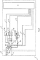
- Fig. 1 shows a block diagram of a conventional from the prior art already known I / O device, which consists of three individual terminals 2a, 2b, 2c with a total of five terminals 3 and a circuit electronics 4, wherein the middle terminal 2b and the lower terminal 2c a have joint Anschiuss 3.
- the circuit electronics 4 has a relay 20, a signal generator 10, three diodes 21, wherein the relay 20 is controlled by means of a first control signal 7 from the logic unit 8 and the signal generator 10, the presence of an active input signal 19 or passive input signal 5 by means of a Status signal 12 to the logic unit 8 supplies.
- diodes 21 serve here as reverse polarity protection.
- the following functions are now realized: at the top terminal 2a, a connected externally driven load 18 by means of the relay 20 and the first control signal 7 via a logic unit 8 as needed controlled or designed; at the middle terminal 2b, the presence or absence of a passive input signal 5 is detected; at the lower terminal 2c, the presence or absence of an active input signal 19 is detected.
- Fig. 2 1 shows a block diagram of an embodiment of the multifunctional I / O device 1 according to the invention.
- This consists of a connection terminal 2 with two terminals 3 and a circuit electronic unit 4.
- the connection terminal 2 serves either to control or to switch a connected externally driven load 18, or to detect a passive input signal 5 or active input signal 19 applied to the terminals 3 of the connection terminal 2.
- a connected externally driven load 18 may be mentioned here: PLC, contactor, motor, pump, valve, indicator, siren or similar signal generator.
- the active input signal 19 may be an active input signal 19 or passive input signal 5, which is applied to the terminals 3 of the terminal 2.
- the active input signal 19 may be both a DC signal and an AC signal.
- an active input signal 19 should be understood to mean that this signal is able to provide the signal generator 10 with sufficient energy so that it can be operated appropriately.
- a passive input signal 5 is to be understood as a signal which is not able to supply the signal generator with sufficient energy to operate it expediently. This As a result, in this case, an additional energy source 13 is needed for the proper operation of the signal generator 10, which provides the required energy.
- the Scllaltungselektronik 4 consists of several individual components, which will be discussed in more detail below.
- the switching element 6, which typically consists of at least one relay and is controlled by a logic unit 8 according to the respectively set operating state via the first control signal 7, serves to short the two terminals 3 of the terminal 2 or separate from each other, so as a switch to act for a possible connected externally driven load 18.
- the rectifier device 9 which typically consists of one or more diodes, serves to rectify an active input signal 19 applied as AC voltage at the two terminals 3 of the terminal 2 so as to operate the downstream circuit elements appropriately.
- the signal generator 10 which is controlled via the second control signal 11 from the logic unit according to the respectively set operating state, serves to generate a digital status signal 12 when a passive input signal 5 or an active input signal 19 is applied to the two terminals 3 of the connection terminal 2 and the logic unit 8 to detect in this way the presence or absence of a passive input signal 5 or active input signal 19.
- the status signal 12 which is generated by the signal generator 10 in the presence or absence of a passive input signal 5 or active input signal 19 at the two terminals 3 of the terminal 2 and supplied to the logic unit 8 is, as already mentioned above, a digital signal, which can assume both a logical H level and a logic L level.
- the energy source 13 is activated by the logic unit 8 in the third operating state, while it is deactivated in all other, ie the first operating state and the second operating state.
- the third operating state the presence or absence of a passive input signal 5, which is applied to the terminals of the terminal to be detected. Since the applied passive input signal 5 provides no energy for the proper operation of the signal generator for this purpose, the power source 13 is required. This ensures that as soon as a passive input signal 5 is applied to the terminals 3 of the terminal 2, and thus there is a direct connection between the power source 13 and the signal generator 10 to provide the energy required for the signal generator 10.
- the protection device 15 which typically consists of at least one diode, serves to protect the signal generator 10 from operating improperly during operation of the energy source 13. It should be noted at this point that the protective device 15 does not necessarily have to be in the position shown. Other conceivable positions are in Fig. 2 represented by a dashed box.
- active input signals 19 in a wide voltage range are typically meant signals of 2.5V to 230V, which may be both DC signals and AC signals.
- the logic unit 8 which is typically a microprocessor, serves to control the switching element 6 by means of the first control signal 7 and the signal generator 10 by means of the second control signal 11 and the power source 13 by means of the third control signal 14 in accordance with the respectively set operating state so that it depends are active or inactive from the respectively set operating state.
- the configuration or the selection of the respectively desired operating state can in this case, for example, be so conceived that this happens in a step upstream of the regular operation of the multifunctional I / O device 1.
- This configuration step can be done both in advance, i. before delivery to the later customer, as well as later during regular operation, the multifunctional I / O device 1 for setting the respective desired operating state either by the customer or a service technician done.
- this galvanic separation 16 is in Fig. 6 discussed in more detail.
- Fig. 3 shows a detailed representation of in Fig. 2 shown multifunctional I / O device in the first operating state.
- an externally driven load 18 connected to the terminals 3 of the terminal 2 is controlled or switched.
- the logic unit 8 is preconfigured to the first operating state. This means that the logic unit 8 with the aid of the second control signal 11, the signal generator 10 and with the aid of the third control signal 14, the power source 13 is deactivated.
- the second control signal 11 is separated from the logic unit 8 via a galvanic isolation 16a and the third control signal 14 via a further galvanic isolation 16c. This should not be discussed further here, but only in the description of the Fig. 6 ,
- the diode 21a and the diode 21b serve as a rectifier device and the diodes 21c and turn the diode 21b as a protective device.
- the diode 21b has a dual function and is used for both rectification and protection.
- externally driven loads include: PLC, contactor, motor, pump, valve, indicator light, siren or similar signaling devices.
- Fig. 4 shows a detailed representation of in Fig. 2 shown multifunctional I / O device in the second operating state.
- the structure of the multifunctional I / O device 1 is according to the structure as shown in FIG Fig. 3 is shown, only the externally driven load 18 was through replaced an active input signal 19, since the multifunctional I / O device 1 detects a DC or AC signal as an active input signal 19 at the terminals 3 of the terminal 2 in the second operating state.
- the logic unit 8 is preconfigured to this second operating state and again the relevant signal paths are highlighted in bold.
- the signal generator 10 outputs an L level as the status signal 12 to the logic unit 8. In this way, in the second operating state, the logic unit 8 detects the presence or absence of an active input signal 19 at the terminals 3 of the connection terminal 2.
- Fig. 5 shows a detailed representation of in Fig. 2 shown in the third operating state multifunctional I / O device.
- the construction of the multifunctional I / O device 1 is according to the structure as shown in FIG Fig. 3 only the externally driven load 18 has been replaced by a passive input signal 5, since the multifunctional I / O device 1 detects a passive input signal 5 at the terminals 3 of the connection terminal 2 in the third operating state.
- the logic unit 8 is preconfigured to this third operating state and again the relevant signal paths are highlighted in bold.
- the logic unit 8 deactivates the relay 20 via the first control signal 7 and activates the signal generator 10 via the second control signal 11 and the energy source 13 via the third control signal 14.
- the energy source 13 provides the energy required for the purposeful operation of the signal generator 10, since the passive input signal 5 at the two terminals 3 of the connection terminal 2 does not provide enough energy to operate the signal generator 10 expediently.
- the L-level is supplied as a status signal 12 to the logic unit 8 by the signal generator 10.
- the logic unit 8 detects the presence or absence of a passive input signal 5 at the terminals 3 of the connection terminal 2.
- Fig. 6 shows a second embodiment of the multifunctional I / O device according to the invention.
- This redundancy has no influence on the above-described functions of the multifunctional I / O device 1, but has the advantage of satisfying the safety requirements according to the SIL (Safety Integrity Level) standard.
- SIL Safety Integrity Level
- These safety requirements are important in process automation in order to increase the security through the double or if necessary.
- the diversity of design is to ensure that a safety-critical failure of the device as well as the occurrence of simultaneously occurring systematic errors in the measured value provision is excluded with high probability.
- the multifunctional I / O device in hazardous areas, such as the EX zone II.
- the third control signal 14 for controlling the power source 13 means inductive galvanêt separation 16c, for example, a transformer, or by means of capacitive galvanic isolation 16c, for example a Charge pump to realize.
- the galvanic isolation of the first control signal 7 takes place in the relay 6 and the relay 6 'per se and is in the Fig. 6 not shown in detail.
Landscapes
- Engineering & Computer Science (AREA)
- Physics & Mathematics (AREA)
- General Physics & Mathematics (AREA)
- Theoretical Computer Science (AREA)
- Automation & Control Theory (AREA)
- General Engineering & Computer Science (AREA)
- Quality & Reliability (AREA)
- Computing Systems (AREA)
- Direct Current Feeding And Distribution (AREA)
- Control Of Voltage And Current In General (AREA)
- Rectifiers (AREA)
- Logic Circuits (AREA)
- Emergency Protection Circuit Devices (AREA)
Claims (8)
- Dispositif d'E/S multifonctionnel (1), comportant une borne de raccordement (2) avec deux connexions (3) et une électronique de commutation (4), laquelle détecte au moyen de plusieurs états de fonctionnement réglables un signal d'entrée actif (19) ou un signal d'entrée passif (5) présent sur les deux connexions (3) de la borne de raccordement (2), ou commande / commute une charge externe (18), qui est raccordée aux deux connexions de la borne de raccordement, l'électronique de commutation (4) comportant les éléments suivants :au moins un élément de commutation (6), lequel est contrôlable au moyen d'un premier signal de commande (7) d'une unité logique (8), de telle sorte qu'il court-circuite ou sépare les deux connexions (3) de la borne de raccordement (2),un générateur de signaux (10), lequel est contrôlable au moyen d'un deuxième signal de commande (11) de l'unité logique (8), de telle sorte qu'en présence du signal d'entrée actif (19), lequel est en mesure d'acheminer au générateur de signaux (10) suffisamment d'énergie afin que celui-ci puisse fonctionner correctement, ou qu'en présence du signal d'entrée passif (5), lequel n'est pas en mesure d'acheminer au générateur de signaux (10) suffisamment d'énergie afin que celui-ci puisse fonctionner correctement, il génère un signal d'état (12) et achemine ce dernier à l'unité logique (8),une source d'énergie (13), laquelle est contrôlable au moyen d'un troisième signal de commande (14) de l'unité logique (8), de telle sorte qu'en présence du signal d'entrée passif (5) sur les deux connexions (3) de la borne de raccordement (2), la source met à disposition l'énergie nécessaire pour le fonctionnement du générateur de signaux (10),un dispositif de protection (15), qui est couplé entre le générateur de signaux (10) et la source d'énergie (13),l'unité logique (8), laquelle fait la distinction, selon l'état de fonctionnement réglé de l'électronique de commutation (4), entre un premier état de fonctionnement (I), un deuxième état de fonctionnement (II) et un troisième état de fonctionnement (III), et commande, à l'aide du premier signal de commande (7), du deuxième signal de commande (11) et du troisième signal de commande (14), l'élément de commutation (6), le générateur de signaux (10) et la source d'énergie (13) en fonction de l'état de fonctionnement réglé.
- Dispositif selon la revendication 1, pour lequel est prévu un dispositif redresseur (9), lequel redresse, en présence d'une tension alternative en tant que signal d'entrée passif (5) ou signal d'entrée actif (19), le signal d'entrée passif (5) ou le signal d'entrée actif (19) présent, et achemine le signal d'entrée passif (5) ou le signal d'entrée actif (19) au générateur de signaux (10) couplé en aval.
- Dispositif selon la revendication 1, pour lequel, dans le premier état de fonctionnement (I), le générateur de signaux (10) et la source d'énergie (13) sont inactifs et l'unité logique (8) commute l'élément de commutation (6) en fonction de la demande, afin de commander la charge externe connectée (18) entre les deux connexions (3) de la borne de raccordement (2).
- Dispositif selon la revendication 1 et 2, pour lequel dans le deuxième état de fonctionnement (II), l'élément de commutation (6) et la source d'énergie (13) sont inactifs et le générateur de signaux (10) est actif, afin de détecter le signal d'entrée actif (19) entre les deux connexions (3) de la borne de raccordement et de générer à l'aide du générateur de signaux (10) un signal d'état (12) et de l'acheminer à l'unité logique (8).
- Dispositif selon la revendication 1, pour lequel, dans le troisième état de fonctionnement (III), l'élément de commutation (6) est inactif et le générateur de signaux (10) et la source d'énergie (13) sont actifs, afin de détecter le signal d'entrée passif (5) entre les deux connexions (3) de la borne de raccordement (2) et de générer à l'aide du générateur de signaux (10) un signal d'état (12) et de l'acheminer à l'unité logique (8).
- Dispositif selon l'une ou plusieurs des revendications précédentes, pour lequel est prévu en outre - dans la branche de circuit comprenant le dispositif redresseur (9), le générateur de signaux (10) et le dispositif de protection (15) - un élément de limitation de courant (17) destiné à la limitation et/ou à la régulation du courant dans cette branche de circuit.
- Dispositif selon l'une ou plusieurs des revendications précédentes, pour lequel l'élément de commutation (6) et le premier signal de commande (7) correspondant sont conçus de façon redondante.
- Dispositif selon l'une ou plusieurs des revendications précédentes, pour lequel le premier signal de commande (7), le deuxième signal de commande (11), le troisième signal de commande (14) et le signal d'état (12) sont séparés de l'unité logique (8) au moyen d'une séparation galvanique (16).
Applications Claiming Priority (2)
| Application Number | Priority Date | Filing Date | Title |
|---|---|---|---|
| DE102012101615A DE102012101615A1 (de) | 2012-02-28 | 2012-02-28 | Multifunktionale I/O-Vorrichtung |
| PCT/EP2013/051869 WO2013127591A2 (fr) | 2012-02-28 | 2013-01-31 | Dispositif d'entrée/sortie multifonction |
Publications (3)
| Publication Number | Publication Date |
|---|---|
| EP2820738A2 EP2820738A2 (fr) | 2015-01-07 |
| EP2820738B1 true EP2820738B1 (fr) | 2018-03-07 |
| EP2820738B8 EP2820738B8 (fr) | 2018-05-02 |
Family
ID=47678754
Family Applications (1)
| Application Number | Title | Priority Date | Filing Date |
|---|---|---|---|
| EP13702985.6A Active EP2820738B8 (fr) | 2012-02-28 | 2013-01-31 | Dispositif d'entrée/sortie multifonction |
Country Status (5)
| Country | Link |
|---|---|
| US (1) | US9436573B2 (fr) |
| EP (1) | EP2820738B8 (fr) |
| CN (1) | CN104170203B (fr) |
| DE (1) | DE102012101615A1 (fr) |
| WO (1) | WO2013127591A2 (fr) |
Families Citing this family (1)
| Publication number | Priority date | Publication date | Assignee | Title |
|---|---|---|---|---|
| DE102017201166A1 (de) * | 2017-01-25 | 2018-07-26 | Festo Ag & Co. Kg | Kommunikationseinrichtung und System |
Family Cites Families (8)
| Publication number | Priority date | Publication date | Assignee | Title |
|---|---|---|---|---|
| US4771403A (en) * | 1984-11-16 | 1988-09-13 | Allen-Bradley Company, Inc. | I/O module with multi-function integrated circuits and an isolation interface for multiplexing data between a main processor and I/O devices |
| US5479618A (en) * | 1991-07-24 | 1995-12-26 | Allen-Bradley Company, Inc. | I/O module with reduced isolation circuitry |
| US6308231B1 (en) * | 1998-09-29 | 2001-10-23 | Rockwell Automation Technologies, Inc. | Industrial control systems having input/output circuits with programmable input/output characteristics |
| US6320494B1 (en) * | 2000-01-18 | 2001-11-20 | Honeywell International Inc. | Full duplex communication system with power transfer on one pair of conductors |
| WO2002008867A2 (fr) * | 2000-07-25 | 2002-01-31 | Dutec, Inc. | Système, dispositif et procédé d'interface d'entrées/sorties globale entre process ou transducteurs de la machine et le dispositif ou système de régulation |
| EP1500992B1 (fr) * | 2003-07-21 | 2005-11-09 | Siemens Schweiz AG | Dispositif de commande d'appareils de terrain pour une installation technique dans un système d'automatisation de bâtiments |
| DE102005055546A1 (de) * | 2005-11-18 | 2007-05-24 | Endress + Hauser Wetzer Gmbh + Co Kg | Vorrichtung zur Übertragung eines Stromes und/oder eines Signals |
| DE102006052291A1 (de) * | 2006-11-03 | 2008-05-15 | Endress + Hauser Gmbh + Co. Kg | Vorrichtung zur Bestimmung und/oder Überwachung des Füllstandes eines Mediums |
-
2012
- 2012-02-28 DE DE102012101615A patent/DE102012101615A1/de not_active Withdrawn
-
2013
- 2013-01-31 EP EP13702985.6A patent/EP2820738B8/fr active Active
- 2013-01-31 WO PCT/EP2013/051869 patent/WO2013127591A2/fr active Application Filing
- 2013-01-31 US US14/380,006 patent/US9436573B2/en active Active
- 2013-01-31 CN CN201380011344.6A patent/CN104170203B/zh active Active
Non-Patent Citations (1)
| Title |
|---|
| None * |
Also Published As
| Publication number | Publication date |
|---|---|
| CN104170203A (zh) | 2014-11-26 |
| WO2013127591A2 (fr) | 2013-09-06 |
| US20150019763A1 (en) | 2015-01-15 |
| WO2013127591A3 (fr) | 2013-11-21 |
| EP2820738B8 (fr) | 2018-05-02 |
| US9436573B2 (en) | 2016-09-06 |
| DE102012101615A1 (de) | 2013-08-29 |
| CN104170203B (zh) | 2017-09-29 |
| EP2820738A2 (fr) | 2015-01-07 |
Similar Documents
| Publication | Publication Date | Title |
|---|---|---|
| EP2017869B1 (fr) | Dispositif de sécurité destiné à la commande à plusieurs canaux d'un dispositif de sécurité | |
| EP1493064B2 (fr) | Appareil de coupure, protegee contre les erreurs, d'un consommateur electrique, notamment dans les installations de production industrielle | |
| EP2834826B1 (fr) | Dispositif de commutation de sécurite comprenant élément de commutation combiné intégré dans une voie de courant comprenant contacts auxiliaires | |
| DE102013101050A1 (de) | Sicherheitsschaltvorrichtung mit sicherem Netzteil | |
| EP1869687A1 (fr) | Dispositif de coupure de securite servant a deconnecter un recepteur electrique de maniere sure | |
| DE102006030448B4 (de) | Sichere Ausgangsschaltung mit einem einkanaligen Peripherieanschluss für den Ausgang eines Bus-Teilnehmers | |
| EP1989470A1 (fr) | Concept de sécurité pour un dispositif de positionnement à engrenage | |
| EP2587512B1 (fr) | Commutateur orienté vers la sécurité | |
| DE10152653B4 (de) | Vorrichtung zur eigensicheren redundanten Strom-Spannungsversorgung | |
| EP1364459B1 (fr) | Dispositif de commutation de securite | |
| EP2820738B1 (fr) | Dispositif d'entrée/sortie multifonction | |
| DE212012000249U1 (de) | Vorrichtung zum eigensicheren Versorgen, Ansteuern und/oder Auswerten von Feldgeräten im explosionsgeschützten Bereich | |
| EP2433184B1 (fr) | Système de commande permettant de commander un processus | |
| EP3695475B1 (fr) | Module de protection et système de bus de terrain avec module de protection | |
| EP2237118B1 (fr) | Système de sécurité destiné à sécuriser la commande protégée contre l'erreur d'installations électriques et commande de sécurité équipée de celui-ci | |
| DE102007052512B3 (de) | Steuereinrichtung für eine Sicherheitsschaltvorrichtung, Sicherheitsschaltvorrichtung, Verwendung einer Steuereinrichtung und Verfahren zum Steuern einer Sicherheitsschaltvorrichtung | |
| EP2048555A1 (fr) | Dispositif de sortie analogique avec detection d'erreurs | |
| DE102013203731A1 (de) | Fahrzeug-Steuergerät zur Steuerung und Versorgung eines oder mehrerer Verbraucher | |
| WO2020079132A1 (fr) | Appareil de commutation pour commander l'alimentation en énergie d'un récepteur électrique | |
| DE102017221793A1 (de) | Sicherungstechnische Einrichtung für eine sicherungstechnische Anlage | |
| EP2239850B1 (fr) | Dispositif de commande et procédé de commande correspondant destiné à la commande d'un dispositif électrique | |
| EP3346352B1 (fr) | Groupe fonctionnel électronique | |
| EP3048498B1 (fr) | Procédé de lecture de données de diagnostic provenant d'une commande de sécurité | |
| DE10344070A1 (de) | Antriebsmodul für eine Druckmaschine | |
| EP4321949A1 (fr) | Dispositif de commande modulaire |
Legal Events
| Date | Code | Title | Description |
|---|---|---|---|
| PUAI | Public reference made under article 153(3) epc to a published international application that has entered the european phase |
Free format text: ORIGINAL CODE: 0009012 |
|
| 17P | Request for examination filed |
Effective date: 20140708 |
|
| AK | Designated contracting states |
Kind code of ref document: A2 Designated state(s): AL AT BE BG CH CY CZ DE DK EE ES FI FR GB GR HR HU IE IS IT LI LT LU LV MC MK MT NL NO PL PT RO RS SE SI SK SM TR |
|
| AX | Request for extension of the european patent |
Extension state: BA ME |
|
| RIN1 | Information on inventor provided before grant (corrected) |
Inventor name: PAUL, TOBIAS Inventor name: STIB, RALPH Inventor name: ZENUNI, ARMEND |
|
| DAX | Request for extension of the european patent (deleted) | ||
| STAA | Information on the status of an ep patent application or granted ep patent |
Free format text: STATUS: EXAMINATION IS IN PROGRESS |
|
| 17Q | First examination report despatched |
Effective date: 20170210 |
|
| GRAP | Despatch of communication of intention to grant a patent |
Free format text: ORIGINAL CODE: EPIDOSNIGR1 |
|
| STAA | Information on the status of an ep patent application or granted ep patent |
Free format text: STATUS: GRANT OF PATENT IS INTENDED |
|
| INTG | Intention to grant announced |
Effective date: 20171030 |
|
| GRAS | Grant fee paid |
Free format text: ORIGINAL CODE: EPIDOSNIGR3 |
|
| GRAA | (expected) grant |
Free format text: ORIGINAL CODE: 0009210 |
|
| STAA | Information on the status of an ep patent application or granted ep patent |
Free format text: STATUS: THE PATENT HAS BEEN GRANTED |
|
| AK | Designated contracting states |
Kind code of ref document: B1 Designated state(s): AL AT BE BG CH CY CZ DE DK EE ES FI FR GB GR HR HU IE IS IT LI LT LU LV MC MK MT NL NO PL PT RO RS SE SI SK SM TR |
|
| REG | Reference to a national code |
Ref country code: GB Ref legal event code: FG4D Free format text: NOT ENGLISH |
|
| REG | Reference to a national code |
Ref country code: CH Ref legal event code: EP Ref country code: AT Ref legal event code: REF Ref document number: 977529 Country of ref document: AT Kind code of ref document: T Effective date: 20180315 |
|
| REG | Reference to a national code |
Ref country code: DE Ref legal event code: R096 Ref document number: 502013009601 Country of ref document: DE |
|
| REG | Reference to a national code |
Ref country code: IE Ref legal event code: FG4D Free format text: LANGUAGE OF EP DOCUMENT: GERMAN |
|
| RAP2 | Party data changed (patent owner data changed or rights of a patent transferred) |
Owner name: ENDRESS+HAUSER SE+CO. KG |
|
| REG | Reference to a national code |
Ref country code: NL Ref legal event code: MP Effective date: 20180307 |
|
| REG | Reference to a national code |
Ref country code: LT Ref legal event code: MG4D |
|
| PG25 | Lapsed in a contracting state [announced via postgrant information from national office to epo] |
Ref country code: HR Free format text: LAPSE BECAUSE OF FAILURE TO SUBMIT A TRANSLATION OF THE DESCRIPTION OR TO PAY THE FEE WITHIN THE PRESCRIBED TIME-LIMIT Effective date: 20180307 Ref country code: LT Free format text: LAPSE BECAUSE OF FAILURE TO SUBMIT A TRANSLATION OF THE DESCRIPTION OR TO PAY THE FEE WITHIN THE PRESCRIBED TIME-LIMIT Effective date: 20180307 Ref country code: ES Free format text: LAPSE BECAUSE OF FAILURE TO SUBMIT A TRANSLATION OF THE DESCRIPTION OR TO PAY THE FEE WITHIN THE PRESCRIBED TIME-LIMIT Effective date: 20180307 Ref country code: CY Free format text: LAPSE BECAUSE OF FAILURE TO SUBMIT A TRANSLATION OF THE DESCRIPTION OR TO PAY THE FEE WITHIN THE PRESCRIBED TIME-LIMIT Effective date: 20180307 Ref country code: FI Free format text: LAPSE BECAUSE OF FAILURE TO SUBMIT A TRANSLATION OF THE DESCRIPTION OR TO PAY THE FEE WITHIN THE PRESCRIBED TIME-LIMIT Effective date: 20180307 Ref country code: NO Free format text: LAPSE BECAUSE OF FAILURE TO SUBMIT A TRANSLATION OF THE DESCRIPTION OR TO PAY THE FEE WITHIN THE PRESCRIBED TIME-LIMIT Effective date: 20180607 |
|
| PG25 | Lapsed in a contracting state [announced via postgrant information from national office to epo] |
Ref country code: RS Free format text: LAPSE BECAUSE OF FAILURE TO SUBMIT A TRANSLATION OF THE DESCRIPTION OR TO PAY THE FEE WITHIN THE PRESCRIBED TIME-LIMIT Effective date: 20180307 Ref country code: BG Free format text: LAPSE BECAUSE OF FAILURE TO SUBMIT A TRANSLATION OF THE DESCRIPTION OR TO PAY THE FEE WITHIN THE PRESCRIBED TIME-LIMIT Effective date: 20180607 Ref country code: GR Free format text: LAPSE BECAUSE OF FAILURE TO SUBMIT A TRANSLATION OF THE DESCRIPTION OR TO PAY THE FEE WITHIN THE PRESCRIBED TIME-LIMIT Effective date: 20180608 Ref country code: SE Free format text: LAPSE BECAUSE OF FAILURE TO SUBMIT A TRANSLATION OF THE DESCRIPTION OR TO PAY THE FEE WITHIN THE PRESCRIBED TIME-LIMIT Effective date: 20180307 Ref country code: LV Free format text: LAPSE BECAUSE OF FAILURE TO SUBMIT A TRANSLATION OF THE DESCRIPTION OR TO PAY THE FEE WITHIN THE PRESCRIBED TIME-LIMIT Effective date: 20180307 |
|
| PG25 | Lapsed in a contracting state [announced via postgrant information from national office to epo] |
Ref country code: MT Free format text: LAPSE BECAUSE OF FAILURE TO SUBMIT A TRANSLATION OF THE DESCRIPTION OR TO PAY THE FEE WITHIN THE PRESCRIBED TIME-LIMIT Effective date: 20180307 |
|
| PG25 | Lapsed in a contracting state [announced via postgrant information from national office to epo] |
Ref country code: AL Free format text: LAPSE BECAUSE OF FAILURE TO SUBMIT A TRANSLATION OF THE DESCRIPTION OR TO PAY THE FEE WITHIN THE PRESCRIBED TIME-LIMIT Effective date: 20180307 Ref country code: RO Free format text: LAPSE BECAUSE OF FAILURE TO SUBMIT A TRANSLATION OF THE DESCRIPTION OR TO PAY THE FEE WITHIN THE PRESCRIBED TIME-LIMIT Effective date: 20180307 Ref country code: NL Free format text: LAPSE BECAUSE OF FAILURE TO SUBMIT A TRANSLATION OF THE DESCRIPTION OR TO PAY THE FEE WITHIN THE PRESCRIBED TIME-LIMIT Effective date: 20180307 Ref country code: PL Free format text: LAPSE BECAUSE OF FAILURE TO SUBMIT A TRANSLATION OF THE DESCRIPTION OR TO PAY THE FEE WITHIN THE PRESCRIBED TIME-LIMIT Effective date: 20180307 Ref country code: EE Free format text: LAPSE BECAUSE OF FAILURE TO SUBMIT A TRANSLATION OF THE DESCRIPTION OR TO PAY THE FEE WITHIN THE PRESCRIBED TIME-LIMIT Effective date: 20180307 |
|
| PG25 | Lapsed in a contracting state [announced via postgrant information from national office to epo] |
Ref country code: SK Free format text: LAPSE BECAUSE OF FAILURE TO SUBMIT A TRANSLATION OF THE DESCRIPTION OR TO PAY THE FEE WITHIN THE PRESCRIBED TIME-LIMIT Effective date: 20180307 Ref country code: SM Free format text: LAPSE BECAUSE OF FAILURE TO SUBMIT A TRANSLATION OF THE DESCRIPTION OR TO PAY THE FEE WITHIN THE PRESCRIBED TIME-LIMIT Effective date: 20180307 Ref country code: CZ Free format text: LAPSE BECAUSE OF FAILURE TO SUBMIT A TRANSLATION OF THE DESCRIPTION OR TO PAY THE FEE WITHIN THE PRESCRIBED TIME-LIMIT Effective date: 20180307 |
|
| REG | Reference to a national code |
Ref country code: DE Ref legal event code: R097 Ref document number: 502013009601 Country of ref document: DE |
|
| PG25 | Lapsed in a contracting state [announced via postgrant information from national office to epo] |
Ref country code: PT Free format text: LAPSE BECAUSE OF FAILURE TO SUBMIT A TRANSLATION OF THE DESCRIPTION OR TO PAY THE FEE WITHIN THE PRESCRIBED TIME-LIMIT Effective date: 20180709 |
|
| PLBE | No opposition filed within time limit |
Free format text: ORIGINAL CODE: 0009261 |
|
| STAA | Information on the status of an ep patent application or granted ep patent |
Free format text: STATUS: NO OPPOSITION FILED WITHIN TIME LIMIT |
|
| PG25 | Lapsed in a contracting state [announced via postgrant information from national office to epo] |
Ref country code: DK Free format text: LAPSE BECAUSE OF FAILURE TO SUBMIT A TRANSLATION OF THE DESCRIPTION OR TO PAY THE FEE WITHIN THE PRESCRIBED TIME-LIMIT Effective date: 20180307 |
|
| 26N | No opposition filed |
Effective date: 20181210 |
|
| PG25 | Lapsed in a contracting state [announced via postgrant information from national office to epo] |
Ref country code: SI Free format text: LAPSE BECAUSE OF FAILURE TO SUBMIT A TRANSLATION OF THE DESCRIPTION OR TO PAY THE FEE WITHIN THE PRESCRIBED TIME-LIMIT Effective date: 20180307 |
|
| PG25 | Lapsed in a contracting state [announced via postgrant information from national office to epo] |
Ref country code: MC Free format text: LAPSE BECAUSE OF FAILURE TO SUBMIT A TRANSLATION OF THE DESCRIPTION OR TO PAY THE FEE WITHIN THE PRESCRIBED TIME-LIMIT Effective date: 20180307 |
|
| REG | Reference to a national code |
Ref country code: CH Ref legal event code: PL |
|
| GBPC | Gb: european patent ceased through non-payment of renewal fee |
Effective date: 20190131 |
|
| PG25 | Lapsed in a contracting state [announced via postgrant information from national office to epo] |
Ref country code: LU Free format text: LAPSE BECAUSE OF NON-PAYMENT OF DUE FEES Effective date: 20190131 |
|
| REG | Reference to a national code |
Ref country code: BE Ref legal event code: MM Effective date: 20190131 |
|
| REG | Reference to a national code |
Ref country code: IE Ref legal event code: MM4A |
|
| PG25 | Lapsed in a contracting state [announced via postgrant information from national office to epo] |
Ref country code: BE Free format text: LAPSE BECAUSE OF NON-PAYMENT OF DUE FEES Effective date: 20190131 |
|
| PG25 | Lapsed in a contracting state [announced via postgrant information from national office to epo] |
Ref country code: LI Free format text: LAPSE BECAUSE OF NON-PAYMENT OF DUE FEES Effective date: 20190131 Ref country code: GB Free format text: LAPSE BECAUSE OF NON-PAYMENT OF DUE FEES Effective date: 20190131 Ref country code: CH Free format text: LAPSE BECAUSE OF NON-PAYMENT OF DUE FEES Effective date: 20190131 |
|
| PG25 | Lapsed in a contracting state [announced via postgrant information from national office to epo] |
Ref country code: IE Free format text: LAPSE BECAUSE OF NON-PAYMENT OF DUE FEES Effective date: 20190131 |
|
| REG | Reference to a national code |
Ref country code: AT Ref legal event code: MM01 Ref document number: 977529 Country of ref document: AT Kind code of ref document: T Effective date: 20190131 |
|
| PG25 | Lapsed in a contracting state [announced via postgrant information from national office to epo] |
Ref country code: TR Free format text: LAPSE BECAUSE OF FAILURE TO SUBMIT A TRANSLATION OF THE DESCRIPTION OR TO PAY THE FEE WITHIN THE PRESCRIBED TIME-LIMIT Effective date: 20180307 |
|
| PG25 | Lapsed in a contracting state [announced via postgrant information from national office to epo] |
Ref country code: AT Free format text: LAPSE BECAUSE OF NON-PAYMENT OF DUE FEES Effective date: 20190131 |
|
| PG25 | Lapsed in a contracting state [announced via postgrant information from national office to epo] |
Ref country code: IS Free format text: LAPSE BECAUSE OF FAILURE TO SUBMIT A TRANSLATION OF THE DESCRIPTION OR TO PAY THE FEE WITHIN THE PRESCRIBED TIME-LIMIT Effective date: 20180707 |
|
| PG25 | Lapsed in a contracting state [announced via postgrant information from national office to epo] |
Ref country code: HU Free format text: LAPSE BECAUSE OF FAILURE TO SUBMIT A TRANSLATION OF THE DESCRIPTION OR TO PAY THE FEE WITHIN THE PRESCRIBED TIME-LIMIT; INVALID AB INITIO Effective date: 20130131 |
|
| PG25 | Lapsed in a contracting state [announced via postgrant information from national office to epo] |
Ref country code: MK Free format text: LAPSE BECAUSE OF FAILURE TO SUBMIT A TRANSLATION OF THE DESCRIPTION OR TO PAY THE FEE WITHIN THE PRESCRIBED TIME-LIMIT Effective date: 20180307 |
|
| PGFP | Annual fee paid to national office [announced via postgrant information from national office to epo] |
Ref country code: FR Payment date: 20230124 Year of fee payment: 11 |
|
| PGFP | Annual fee paid to national office [announced via postgrant information from national office to epo] |
Ref country code: IT Payment date: 20230120 Year of fee payment: 11 |
|
| P01 | Opt-out of the competence of the unified patent court (upc) registered |
Effective date: 20230601 |
|
| PGFP | Annual fee paid to national office [announced via postgrant information from national office to epo] |
Ref country code: DE Payment date: 20240119 Year of fee payment: 12 |