EP2819182A1 - Semiconductor light-emitting element - Google Patents
Semiconductor light-emitting element Download PDFInfo
- Publication number
- EP2819182A1 EP2819182A1 EP13751123.4A EP13751123A EP2819182A1 EP 2819182 A1 EP2819182 A1 EP 2819182A1 EP 13751123 A EP13751123 A EP 13751123A EP 2819182 A1 EP2819182 A1 EP 2819182A1
- Authority
- EP
- European Patent Office
- Prior art keywords
- layer
- light emitting
- phase changing
- refractive index
- layers
- Prior art date
- Legal status (The legal status is an assumption and is not a legal conclusion. Google has not performed a legal analysis and makes no representation as to the accuracy of the status listed.)
- Granted
Links
- 239000004065 semiconductor Substances 0.000 title claims abstract description 52
- 239000000758 substrate Substances 0.000 claims abstract description 24
- 230000002708 enhancing effect Effects 0.000 abstract description 8
- 239000010410 layer Substances 0.000 description 358
- 239000010408 film Substances 0.000 description 47
- 238000004088 simulation Methods 0.000 description 38
- 238000001228 spectrum Methods 0.000 description 37
- 230000000052 comparative effect Effects 0.000 description 13
- 230000000694 effects Effects 0.000 description 13
- 238000013461 design Methods 0.000 description 11
- 238000003780 insertion Methods 0.000 description 10
- 230000037431 insertion Effects 0.000 description 10
- 239000000203 mixture Substances 0.000 description 10
- 238000010586 diagram Methods 0.000 description 9
- 238000000034 method Methods 0.000 description 9
- 229910000980 Aluminium gallium arsenide Inorganic materials 0.000 description 7
- 230000003247 decreasing effect Effects 0.000 description 5
- 229910001218 Gallium arsenide Inorganic materials 0.000 description 4
- 238000004519 manufacturing process Methods 0.000 description 4
- 238000004364 calculation method Methods 0.000 description 3
- 239000002346 layers by function Substances 0.000 description 3
- 238000012986 modification Methods 0.000 description 3
- 230000004048 modification Effects 0.000 description 3
- 230000003287 optical effect Effects 0.000 description 3
- 230000015572 biosynthetic process Effects 0.000 description 2
- 239000000463 material Substances 0.000 description 2
- 239000002356 single layer Substances 0.000 description 2
- 229910004205 SiNX Inorganic materials 0.000 description 1
- VYPSYNLAJGMNEJ-UHFFFAOYSA-N Silicium dioxide Chemical compound O=[Si]=O VYPSYNLAJGMNEJ-UHFFFAOYSA-N 0.000 description 1
- 238000010521 absorption reaction Methods 0.000 description 1
- 239000003795 chemical substances by application Substances 0.000 description 1
- 238000011161 development Methods 0.000 description 1
- 230000002349 favourable effect Effects 0.000 description 1
- 238000002488 metal-organic chemical vapour deposition Methods 0.000 description 1
- 239000012788 optical film Substances 0.000 description 1
- 230000000737 periodic effect Effects 0.000 description 1
- 229910052814 silicon oxide Inorganic materials 0.000 description 1
- 125000006850 spacer group Chemical group 0.000 description 1
- 230000001629 suppression Effects 0.000 description 1
- 239000013077 target material Substances 0.000 description 1
- 239000010409 thin film Substances 0.000 description 1
Images






Classifications
-
- H—ELECTRICITY
- H10—SEMICONDUCTOR DEVICES; ELECTRIC SOLID-STATE DEVICES NOT OTHERWISE PROVIDED FOR
- H10H—INORGANIC LIGHT-EMITTING SEMICONDUCTOR DEVICES HAVING POTENTIAL BARRIERS
- H10H20/00—Individual inorganic light-emitting semiconductor devices having potential barriers, e.g. light-emitting diodes [LED]
- H10H20/80—Constructional details
- H10H20/84—Coatings, e.g. passivation layers or antireflective coatings
- H10H20/841—Reflective coatings, e.g. dielectric Bragg reflectors
-
- H—ELECTRICITY
- H10—SEMICONDUCTOR DEVICES; ELECTRIC SOLID-STATE DEVICES NOT OTHERWISE PROVIDED FOR
- H10H—INORGANIC LIGHT-EMITTING SEMICONDUCTOR DEVICES HAVING POTENTIAL BARRIERS
- H10H20/00—Individual inorganic light-emitting semiconductor devices having potential barriers, e.g. light-emitting diodes [LED]
- H10H20/80—Constructional details
- H10H20/81—Bodies
- H10H20/814—Bodies having reflecting means, e.g. semiconductor Bragg reflectors
-
- H—ELECTRICITY
- H10—SEMICONDUCTOR DEVICES; ELECTRIC SOLID-STATE DEVICES NOT OTHERWISE PROVIDED FOR
- H10H—INORGANIC LIGHT-EMITTING SEMICONDUCTOR DEVICES HAVING POTENTIAL BARRIERS
- H10H20/00—Individual inorganic light-emitting semiconductor devices having potential barriers, e.g. light-emitting diodes [LED]
- H10H20/80—Constructional details
- H10H20/85—Packages
- H10H20/855—Optical field-shaping means, e.g. lenses
- H10H20/856—Reflecting means
-
- H—ELECTRICITY
- H10—SEMICONDUCTOR DEVICES; ELECTRIC SOLID-STATE DEVICES NOT OTHERWISE PROVIDED FOR
- H10H—INORGANIC LIGHT-EMITTING SEMICONDUCTOR DEVICES HAVING POTENTIAL BARRIERS
- H10H20/00—Individual inorganic light-emitting semiconductor devices having potential barriers, e.g. light-emitting diodes [LED]
- H10H20/80—Constructional details
- H10H20/81—Bodies
- H10H20/822—Materials of the light-emitting regions
- H10H20/824—Materials of the light-emitting regions comprising only Group III-V materials, e.g. GaP
Definitions
- the present invention is related to a surface emitting type semiconductor light emitting element equipped with a distributed Bragg reflector and an active layer which are sequentially grown on a semiconductor substrate.
- DBR's distributed Bragg Reflectors
- LED's light emitting diodes
- LD's semiconductor lasers
- DBR's distributed Bragg Reflectors
- a semiconductor light emitting element of the surface emitting type DBR's provided as layers above and below a light emitting layer generally contribute to increases in light emitting efficiency by increasing the reflectance of a specific wavelength as structures that increase resonance.
- DBR's are constituted by multiple layered films, in which layers having a relatively high refractive index (high refractive index layers) and layers having a relatively low refractive index (low refractive index layers) are alternately laminated.
- the wavelength which is reflected by a DBR is extremely sensitive to the thicknesses of the films that constitute the DBR. Accordingly, the light emitting efficiency of a semiconductor light emitting element equipped with a DBR depends greatly on the change in emitted light intensity (light emitting efficiency) when the light emitting wavelength shifts. That is, the increase in light emitting efficiency obtained by a DBR and the degree of change in the light emitting efficiency due to shifts in wavelengths are in a trade off relationship.
- Patent Documents 2 and 3 propose methods for solving this problem of variation in light emitting efficiency caused by changes in ambient temperature.
- Patent Document 2 discloses an element configuration in which a plurality of multiple layer film reflecting layers that respectively reflect light having longer wavelengths and light having shorter wavelengths than the light spectrum generated by an active layer under the active layer, to effectively cause the light spectrum to become a wide band light spectrum, thereby reducing the influence of wavelength shift caused by changes in ambient temperature.
- Patent Document 3 discloses an element configuration in which a notch filter constituted by a first multiple layer film layer, a second multiple layer film layer, and a spacer layer provided between these two layers is provided, to reduce the influence of wavelength shift caused by changes in ambient temperature.
- exposure devices in which multiple semiconductor light emitting elements are arranged one dimensionally or two dimensionally, are employed as exposure heads for printers and scanners. Uniformity of light intensity among the arranged plurality of semiconductor light emitting elements is required in such arrayed exposure devices.
- the expression "light intensity” refers to the intensity of light which is integrated across the light emitting wavelength band of the light emitting elements.
- the light intensities emitted by individual semiconductor light emitting elements among a plurality of light emitting elements which are employed in an exposure device also change due to wavelength shifts caused by changes in ambient temperature. Further, a phenomenon that the manner in which the light intensity changes is different for each element has been observed. For this reason, there is a problem that uniformity of light intensities cannot be maintained among a plurality of semiconductor light emitting elements which are employed in an exposure device.
- Patent Document 4 proposes a light emitting device that suppresses changes in light intensity of light emitting elements due to temperature changes, by providing a reflecting layer beneath an active layer, and a surface having recesses and protrusions at a plurality of distances from the reflecting layer above the active layer.
- semiconductor light emitting elements are produced by dividing a wafer, on which various layers are laminated, into a great number of chips, and a great number of semiconductor light emitting elements are produced from a single wafer.
- the film thicknesses of the layered films formed on the wafer are uniform on the surface of the wafer according to design values. In actuality, however, it is difficult to form films uniformly, and fluctuations are generated in the film thicknesses. As a result, portions at which film thicknesses are smaller and greater than design values are generated on a single wafer, and fluctuations in film thicknesses will be present among chips when the wafer is divided into a great number of chips.
- reflected wavelengths shift toward the shorter wavelength side as the film thickness of a DBR shifts toward the thinner direction. Fluctuations in wavelengths reflected by the DBR due to the fluctuations in film thicknesses cause differences in emitted light intensity with respect to emitted wavelengths. In addition, it is considered that the fluctuations in film thicknesses also cause the phenomenon that the changes in light intensity due to changes in ambient temperatures differ among chips.
- the present invention has been developed in view of the foregoing circumstances. It is an object of the present invention to provide a semiconductor light emitting element, in which the light intensity enhancing effect of a DBR is maintained, while fluctuations in light intensity variations in a great number of elements, which are produced from a single wafer, that accompany temperature changes are suppressed.
- a semiconductor light emitting element of the present invention outputs emitted light having a predetermined emitted light peak wavelength ⁇ , and comprises at least:
- the phase changing layer having a thickness of m ⁇ /2n is a continuous portion having a single refractive index.
- a layer having a different refractive index may be included therein, if the thickness thereof is approximately 15nm or less.
- the definition of the thickness m ⁇ /2n includes thicknesses within a range of ⁇ 10% thereof. That is, the thickness of the phase changing layer may be within a range from (m ⁇ /2n) ⁇ 0.9 to (m ⁇ /2n) ⁇ 1.1.
- two phase changing layers are provided within the lower distributed Bragg reflector layer.
- the lower distributed Bragg reflector layer is basically constituted by two or more pairs of a low refractive index layer having a thickness a and a high refractive index layer having a thickness b which are alternately laminated; and for one of the low refractive index layers and the high refractive index layers constituting the phase changing layer to have the thickness m ⁇ /2n.
- the semiconductor light emitting element of the present invention is of a configuration, wherein: a distributed Bragg reflector layer is not provided as a layer above the light emitting layer; and an antireflection layer is provided as a layer above the light emitting layer.
- the semiconductor light emitting element of the present invention is of a configuration, wherein: a distributed Bragg reflector layer is not provided as a layer above the light emitting layer; and the antireflection layer is provided as a layer above the light emitting layer, it is preferable for two of the phase changing layers to be provided within the lower distributed Bragg reflector layer; for one of the two phase changing layers to be one of the low refractive index layer and the high refractive index layer that constitutes the pair most toward the side of the light emitting layer; and for the other of the two phase changing layers to be present within one of a range from 0.24 to 0.46 and a range from 0.66 to 0.82, when the lower distributed Bragg reflector layer is divided into percentages, with the side thereof toward the light emitting layer designated as 0, and the side thereof toward the substrate designated as 1. It is particularly preferable for the other of the two layers to be present within a range from 0.27 to 0.39 within the lower distributed Bragg reflector layer.
- the semiconductor light emitting element of the present invention may further comprise an upper distributed Bragg reflector layer provided as a layer above the light emitting layer.
- the semiconductor light emitting element further comprises the upper distributed Bragg reflector layer provided as a layer above the light emitting layer
- two of the phase changing layers it is preferable for two of the phase changing layers to be provided within the lower distributed Bragg reflecting layer; for one of the two phase changing layers to be one of the low refractive index layer and the high refractive index layer that constitutes the pair most toward the side of the light emitting layer; and for the other of the two phase changing layers to be present within one of a range from 0.22 to 0.33, when the lower distributed Bragg reflecting layer is divided into percentages, with the side thereof toward the light emitting layer designated as 0, and the side thereof toward the substrate designated as 1.
- the semiconductor light emitting element of the present invention can be favorably employed as a light emitting diode of the surface emitting type.
- the semiconductor light emitting element of the present invention outputs emitted light having the predetermined emitted light peak wavelength ⁇ , and comprises at least: the substrate; the lower distributed Bragg reflector layer provided on the substrate; and the light emitting layer provided on the lower distributed Bragg reflector layer; at least one phase changing layer having a thickness of m ⁇ /2n being provided within the lower distributed Bragg reflector layer.
- the reflective bandwidth of the lower distributed Bragg reflector layer can be widened. Therefore, changes in light intensity caused by changes in ambient temperature can be suppressed.
- the light intensity enhancing effect of the DBR is maintained, while fluctuations in film thicknesses when films are formed and changes in light intensity with respect to spectrum shifts due to changes in ambient temperature are suppressed, and light intensity variations in a great number of elements, which are produced from a single wafer, can be suppressed.
- Figure 1 is a schematic sectional view and a partial magnified view that illustrate a semiconductor light emitting element 1 according to an embodiment of the present invention.
- the present semiconductor light emitting element 1 is a semiconductor light emitting element of the surface emitting type, equipped with: a p type substrate 10, a lower distributed Bragg reflector layer 30 (hereinafter, referred to as "lower DBR layer 30"), a p type doped layer 13, a light emitting layer 20, an n type doped layer 15, a contact layer 17, and an antireflection layer 18. As illustrated by the arrow that schematically indicates the path of emitted light, light which is generated in the light emitting layer 20 is reflected by the lower DBR layer 30, passes through the antireflection layer 18, and is emitted from the surface of the element.
- each of the layers is not particularly limited.
- p type GaAs may be employed as the substrate 10
- an AlGaAs type multiple layer semiconductor film may be employed as the lower DBR layer 30
- p type AlGaAs may be employed as the p type doped layer 13
- AlGaAs may be employed as the light emitting layer 20
- n type AlGaAs may be employed as the n type doped layer 15
- n type GaAs may be employed as the contact layer 17
- SiO x or SiN x may be employed as the antireflection layer 18.
- AlGaAs semiconductor layers may be each of the functional layers by varying the compositional ratios between Al and Ga.
- the antireflection layer may be formed by a single layer or formed by a plurality of layers.
- the antireflection layer is constituted by a single layer and the wavelength of light for which reflection is to be suppressed is ⁇
- the refractive index n of the antireflection layer is ⁇ (2L-1)/4n (here, L is an integer 1 or greater).
- the lower DBR layer 30 is a multiple layer film constituted by pairs of a low refractive index layer 31 having a relatively low refractive index and a high refractive index layer 32 having a relatively high refractive index, which are alternately laminated.
- the basic structure of a common DBR layer is a multiple layer film structure in which two or more pairs (a total of four or more layers) of the low refractive index layer 31 having a thickness a and the high refractive index layer 32 having a thickness b are alternately laminated, such that light within a light emitting wavelength band is efficiently reflected.
- the thicknesses a and b of the low refractive index layers 31 and the high refractive index layers 32 are commonly close to ⁇ /4n (here, A is a desired central reflected wavelength, and n is the refractive index of each of the layers).
- the present embodiment is characterized by the lower DBR layer 30 having phase changing layers 33 having a thickness of m ⁇ /2n therein.
- ⁇ is the peak wavelength of emitted light
- n is the refractive index of the phase changing layer with respect to the emitted peak wavelength
- m is an integer one or greater.
- the phase changing layers 33 are constituted by a low refractive index layer composition.
- the film thicknesses in the present specification have allowable error ranges of ⁇ 10% in thickness.
- an upper DBR layer is commonly provided as a layer above a light emitting layer in addition to a lower DBR layer, to adopt a structure in which resonance occurs between the upper and lower DBR layers.
- the semiconductor light emitting element of the present embodiment is of a configuration in which an upper DBR layer is not provided.
- the element having the configuration described above is generally produced by sequentially forming each layer on a wafer by a film forming method such as the MOCVD method, and then dividing the wafer into chips.
- a film forming method such as the MOCVD method
- the fluctuations in thickness vary depending on the type of material and the film forming method, but fluctuations of approximately ⁇ 10% may occur.
- DBR's are extremely sensitive to film thickness. Therefore, the fluctuations in film thicknesses on the wafer become factors that cause fluctuations in the temperature properties of each element which is formed by dividing the wafer into chips.
- elements having the configuration of the present embodiment can maintain the light intensity enhancing effects of the DBR, while greatly suppressing fluctuations in the temperature properties among a plurality of elements obtained from a single wafer.
- phase changing layers 33 having a thickness of m ⁇ /2 are provided within the lower DBR layer 30.
- the advantageous effect of suppressing fluctuations in temperature properties can be obtained even if only a single phase changing layer is provided (refer to Simulation 1 to be described later), compared to a case in which a DBR layer is not provided with the phase changing layer.
- the reflective bandwidth of the lower DBR layer can be widened by providing the phase changing layers 33. It is considered that as a result, the light intensity enhancing effects of the DBR can be maintained, while suppressing fluctuations in light intensities due to temperature changes.
- the first phase changing layer 33 is provided within the pair closest to the light emitting layer 20, as illustrated in the schematic sectional view of the lower DBR layer 30 of Figure 2 .
- the advantageous effect of suppressing fluctuations in temperature properties can be more prominently obtained by positioning the second phase changing layer 33 within a range from 0.24 to 0.46 or a range from 0.66 to 0.82 and particularly within a range from 0.27 to 0.39, when the thickness of the lower DBR layer is divided into percentages, with the side thereof toward the light emitting layer designated as 0, and the side thereof toward the substrate designated as 1, as illustrated in Figure 2 (refer to Simulation 2 to be described later). Note that the thickness of a layer which even partially overlaps these ranges may be set to m ⁇ /2.
- Figure 3 is a schematic sectional view that illustrates a semiconductor light emitting element 2 according to an example of a design modification.
- an upper DBR layer 35 is provided above a light emitting layer 20.
- the configuration of a lower DBR layer 30 is substantially the same as that described above, and the same advantageous effects of obtaining the light intensity enhancing effect while suppressing fluctuations in temperature properties can be obtained.
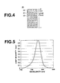
- the preferred ranges of positions at which two phase changing layers are provided in the lower DBR layer 30 differ from the embodiment described above. It is preferable for a first phase changing layer 33 to be provided within the pair closest to the light emitting layer 20, as illustrated in the schematic sectional view of the lower DBR layer 30 of Figure 4 . Meanwhile, it is preferable for a second phase changing layer 33 to be positioned within a range from 0.22 to 0.33, when the thickness of the lower DBR layer is divided into percentages, with the side thereof toward the light emitting layer designated as 0, and the side thereof toward the substrate designated as 1, as illustrated in Figure 4 (refer to Simulation 4 to be described later) .
- the DBR layer and the light emitting layer may be of the same compositional type, in order to prevent complexities during production.
- the phase changing layers may be of a composition completely different from the basic layers that constitute the DBR layer.
- the composition of the high refractive index layers or the composition of the low refractive index layers that constitute the basic DBR layer to be employed as the composition of the phase changing layer, from the viewpoint of simplification of production steps. Note that in the embodiment described above, the thicknesses of the low refractive index layers were changed, but the same advantageous effects can be obtained by changing the thicknesses of the high refractive index layers.
- phase changing layers In addition, in the case that a plurality of the phase changing layers are provided, film formation conditions must be calculated for each composition and film thickness in order to form the phase changing layers of different compositions and/or film thicknesses in actual production. Therefore, this will lead to an increase in development costs. Accordingly, in the case that a plurality of the phase changing layers are formed, they are constituted by layers having the same composition. In addition, the optimal thickness of the phase changing layers is ⁇ /2n (refer to Simulation 3 to be described later), and therefore it is preferable for the thicknesses of the phase changing layers to be the same ( ⁇ /2n).
- phase changing layers having thicknesses of m ⁇ //2n described in the above embodiment may have an extremely thin layer having a thickness of up to approximately 15nm inserted within the interiors thereof (refer to simulation 5 to be described later) .
- the thickness of the inserted layer is up to approximately 15nm, the advantageous effect of suppressing fluctuations in temperature properties can be sufficiently obtained, without losing the function of the phase changing layer.
- a GaAs-AlAs type light emitting element that has a peak wavelength of emitted light of 780nm at room temperature was considered.
- the natural light emitting spectrum of a GaAs-AlAs type light emitting element which was employed is illustrated in Figure 5 .
- the natural light emitting spectrum shifts 10nm toward the long wavelength side (indicated by the broken line in Figure 5 ) when the temperature rises approximately 40°C from room temperature.
- the natural light emitting spectrum is the spectrum of light emitted by a light emitting layer, and is a spectrum which is not influenced by a DBR.
- shifts in thickness vary depending on the type of material and the film forming method, but shifts in thickness of at most approximately ⁇ 10% may occur. Meanwhile, by adjusting film forming conditions and target materials, the shifts in thickness can be suppressed to approximately ⁇ 2.5%. Therefore, the following simulations presume that the shifts in thickness are ⁇ 2.5%.
- the resonator spectrum is the spectrum of light which is output from each element in the case that light having the same intensity for all wavelengths is emitted from a light emitting layer, and is determined unrelated to the light emitting spectrum of the light emitting layer.
- the resonator spectra are derived by simulations that employ inner light emission calculation of multiple layer films that exhibit absorption. Specifically, multiple film layer calculation of externally incident light was performed with reference to Basic Theory of Optical Thin Films (by Mitsunobu Kohiyama, The Optronics Co., Ltd.), and phase differences within the light emitting layers were calculated separately to calculate internal light emission. Note that similar calculations can be reproduced by internal light emission calculating software such as SETFOS by FLUXiM AG.
- the differences between the maximum values and the minimum values are designated as the fluctuations ⁇ in temperature properties (temperature property fluctuations).
- ⁇ Max dPi / dT - Min dPi / dT
- the average light emitting magnification by the DBR layer was derived in the following manner.
- a light emitting intensity P 0 of an LED which is not provided with a DBR layer was obtained, light emitting magnifications Pi/P 0 were calculated for the five elements 1 through 5, and the average value of the light emitting magnifications of the five elements is designated as the average light emitting magnification M. Note that in the following description, the average light emitting magnification is also simply referred to as "light emitting magnification".
- the DBR layers are multiple layer films in which Al 0.3 Ga 0.7 As, which has a relatively high refractive index, and Al 0.9 Ga 0.1 As, which has a relatively low refractive index, are alternately laminated.
- Each set of a high refractive index layer and a low refractive index is designated as one pair, and the lower DBR layers are basically constituted by 19.5 pairs.
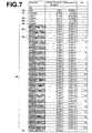
- a light emitting diode having the configuration illustrated in Figure 1 and of which specifics are shown in the table of Figure 7 was considered.
- the reference numerals of Figure 1 indicate which layers in the table of Figure 7 correspond to which functional layer of the LED, and detailed descriptions thereof will be omitted (the same applies in cases that layer structures are shown in tables).
- the LED which was considered has a lower DBR layer 30, an n type doped layer (Al280) 13, a light emitting layer (active) 20, a p type doped layer (Al280) 15, a contact layer 17, and an antireflection layer (SiN) 18, which are provided on a GaAs substrate 10.
- n a is the refractive index of the light emitting layer.
- Al x Ga 1-x As layers are indicated by Al then the numerical value of x multiplied by 1000 (the same applies in the descriptions to follow).
- Al900 represents an Al 0.9 Ga 0.1 As low refractive index layer
- A1300 represents an Al 0.3 Ga 0.7 As high refractive index layer.
- numbers (No.) are sequentially assigned to the Al 0.9 Ga 0.1 As low refractive index layers 31 within the lower DBR layer 30 starting from the side closest to the active layer.
- the low refractive index layer 31 closest to the light emitting layer 20 is No. 1
- the low refractive index layer 31 closest to the substrate is No. 20.
- the element structure which is used as the reference for the light emitting magnification does not have the lower DBR layer 30 shown in the table, and is of a configuration in which only the Al 0.9 Ga 0.1 As layers are provided.
- the results of the simulations are shown in Table 1.
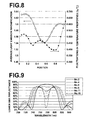
- Table 1 The results of Table 1 are illustrated in the graph of Figure 8 .
- the insertion positions within the DBR layer are indicated as the percentage of the position of the surface of the layer which is converted to the thickness of ⁇ /2n toward the substrate when the surface of the DBR layer most toward the light emitting layer is designated as 0, and the interface thereof with the substrate is designated as 1.
- the reflectance particularly of the central wavelength becomes low depending on the insertion position of the phase changing layer, while at the same time, the reflective bandwidth becomes wider.
- the spectrum shape becomes substantially the same at insertion positions symmetrical to the central position of the DBR (between layer No. 10 and layer No. 11 in the present example; No. 6 and No. 16 of Figure 9 , for example, show spectra which are substantially the same).
- the phase of reflected waves reflected by a DBR layer above the second phase changing layer and the phase of reflected waves reflected by a DBR layer under the second phase changing layer will be in a relationship in which they cancel each other out.
- the number of DBR layers above and below the phase changing layer to be the same, reflected waves of the DBR design wavelength will be substantially completely canceled out, and reflected waves will not be generated.
- the second phase changing layer is inserted at positions other than the central position, it is considered that reflection at the design wavelength will decrease due to a similar phenomenon. Meanwhile, with respect to wavelengths shifted from the DBR design wavelength, reflected waves of these wavelengths are originally in a relationship in which they cancel each other out.
- the relationship in which the reflected waves cancel each other out becomes weaker due to the phase changing layer being inserted, and these wavelengths will be reflected to a certain degree. It is considered that the phase changing layer which is inserted into the lower DBR layer contributes to widening of the reflective spectrum bandwidth in this manner.
- Figure 10 illustrates the values of Table 3 as a graph.
- a light emitting diode (LED) having the structure illustrated in Figure 3 and having the layer structure which is shown in detail in the table of Figure 13 as a layer structure above the light emitting layer 20 was considered.
- the layer structure of layers under the light emitting layer 20 is the same as that of the LED of Simulation 2.
- the reference numerals of Figure 3 indicate which layers in the table of Figure 13 correspond to which functional layer of the LED, and detailed descriptions thereof will be omitted.
- the results are shown in Table 5.
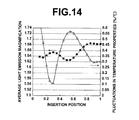
- Figure 14 illustrates the values of Table 5 as a graph.
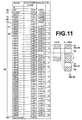
- Example 1 is an LED having the layer structure of Simulation 2 illustrated in Figure 11 , in which the thicknesses t of the No. 1 and No. 7 low refractive index layers are ⁇ /2n.
- the resonator spectrum of this element obtained by simulations is illustrated in Figure 17 .
- the natural light emitting spectrum, the reflectance of the lower DBR layer with respect to the peak light emission wavelength, and the reflectance of the upper AR layer with respect to the peak light emission wavelength are illustrated in Figure 18 .
- Example 2 is an LED having the layer structure illustrated in Figure 19 .
- the resonator spectrum of the present element obtained by simulations is illustrated in Figure 20 .
- Example 3 is an LED having the layer structure of Simulation 5 illustrated in Figure 15 , in which the thickness of the layer 34 inserted into the No. 7 low refractive index layer is 10nm.
- Comparative Example 1 is an LED having the layer structure of the light emitting layer 20 and the layers under the light emitting layer 20 shown in the table of Figure 7 , and the upper DBR layer 35 illustrated in Figure 13 as a layer above the light emitting layer 20. That is, the present element is provided with the lower DBR layer 30 constituted by 19.5 pairs, and the upper DBR layer 35 constituted by 5 pairs, without a phase changing layer having a thickness of m ⁇ /2n.
- the resonator spectrum of the present element obtained by simulations is illustrated in Figure 21 .
- Comparative Example 2 has the layer structure shown in the table of Figure 7 . That is, the present element is provided with a lower DBR layer constituted by 19.5 pairs, an AR structure as a layer above the light emitting layer instead of a DBR layer, without a phase changing layer having a thickness of m ⁇ /2n.
- the resonator spectrum of the present element obtained by simulations is illustrated in Figure 22 .
- Example 1 As shown in Table 7, the fluctuations in temperature properties of Example 1 is 1/20 those of a conventional element structure provided with DBR layers above and below a light emitting layer (Comparative Example 1), and exhibits an extremely high temperature property fluctuation suppressing effect. Both of Examples 1 and 2 can suppress temperature property fluctuations to 0.1%/°C or less. This indicates that the layer having the thickness of ⁇ /2n maybe either a low refractive index layer or a high refractive index layer.
- the semiconductor light emitting element of the present invention will exhibit extremely advantageous effects if applied to an LED array exposure device that employs a plurality of LED's produced on a single wafer and has fluctuations in film thicknesses, in which it is necessary to uniformize the light intensities of the plurality of LED's.
Landscapes
- Led Devices (AREA)
- Semiconductor Lasers (AREA)
Abstract
Description
- The present invention is related to a surface emitting type semiconductor light emitting element equipped with a distributed Bragg reflector and an active layer which are sequentially grown on a semiconductor substrate.
- There are semiconductor light emitting elements, such as light emitting diodes (LED's) and semiconductor lasers (LD's: Laser Diodes) which are configured with DBR's (Distributed Bragg Reflectors) in order to improve the light emitting efficiency thereof (
Patent Documents - Meanwhile, it is known that the light emitting spectra of semiconductor light emitting elements change greatly due to changes in ambient temperature, and that the light emission wavelengths shift toward the longer wavelength side as temperatures become higher. For example, a wavelength shift of approximately 10nm toward the long wavelength side occurs in GaAs-AlAs LED's when the temperature of a utilization environment rises approximately 40°C. For this reason, there is a problem that the light emission intensity of semiconductor light emitting elements equipped with DBR's varies greatly due to changes in ambient temperature.
-
Patent Documents -
Patent Document 2 discloses an element configuration in which a plurality of multiple layer film reflecting layers that respectively reflect light having longer wavelengths and light having shorter wavelengths than the light spectrum generated by an active layer under the active layer, to effectively cause the light spectrum to become a wide band light spectrum, thereby reducing the influence of wavelength shift caused by changes in ambient temperature. -
Patent Document 3 discloses an element configuration in which a notch filter constituted by a first multiple layer film layer, a second multiple layer film layer, and a spacer layer provided between these two layers is provided, to reduce the influence of wavelength shift caused by changes in ambient temperature. - Meanwhile, exposure devices, in which multiple semiconductor light emitting elements are arranged one dimensionally or two dimensionally, are employed as exposure heads for printers and scanners. Uniformity of light intensity among the arranged plurality of semiconductor light emitting elements is required in such arrayed exposure devices. Here, the expression "light intensity" refers to the intensity of light which is integrated across the light emitting wavelength band of the light emitting elements.
- The light intensities emitted by individual semiconductor light emitting elements among a plurality of light emitting elements which are employed in an exposure device also change due to wavelength shifts caused by changes in ambient temperature. Further, a phenomenon that the manner in which the light intensity changes is different for each element has been observed. For this reason, there is a problem that uniformity of light intensities cannot be maintained among a plurality of semiconductor light emitting elements which are employed in an exposure device.
-
Patent Document 4 proposes a light emitting device that suppresses changes in light intensity of light emitting elements due to temperature changes, by providing a reflecting layer beneath an active layer, and a surface having recesses and protrusions at a plurality of distances from the reflecting layer above the active layer. -
- [Patent Document 1]
Japanese Unexamined Patent Publication No.6(1994)-196681 - [Patent Document 2]
Japanese Unexamined Patent Publication No.2009-070929 - [Patent Document 3]
Japanese Unexamined Patent Publication No.2003-332615 - [Patent Document 4]
Japanese Unexamined Patent Publication No.2010-219220 - Generally, semiconductor light emitting elements are produced by dividing a wafer, on which various layers are laminated, into a great number of chips, and a great number of semiconductor light emitting elements are produced from a single wafer. Ideally, the film thicknesses of the layered films formed on the wafer are uniform on the surface of the wafer according to design values. In actuality, however, it is difficult to form films uniformly, and fluctuations are generated in the film thicknesses. As a result, portions at which film thicknesses are smaller and greater than design values are generated on a single wafer, and fluctuations in film thicknesses will be present among chips when the wafer is divided into a great number of chips. Basically, reflected wavelengths shift toward the shorter wavelength side as the film thickness of a DBR shifts toward the thinner direction. Fluctuations in wavelengths reflected by the DBR due to the fluctuations in film thicknesses cause differences in emitted light intensity with respect to emitted wavelengths. In addition, it is considered that the fluctuations in film thicknesses also cause the phenomenon that the changes in light intensity due to changes in ambient temperatures differ among chips.
- The present invention has been developed in view of the foregoing circumstances. It is an object of the present invention to provide a semiconductor light emitting element, in which the light intensity enhancing effect of a DBR is maintained, while fluctuations in light intensity variations in a great number of elements, which are produced from a single wafer, that accompany temperature changes are suppressed.
- A semiconductor light emitting element of the present invention outputs emitted light having a predetermined emitted light peak wavelength λ, and comprises at least:
- a substrate;
- a lower distributed Bragg reflector layer provided on the substrate; and
- a light emitting layer provided on the lower distributed Bragg reflector layer;
- at least one phase changing layer having a thickness of mλ/2n (wherein n is the refractive index of the phase changing layer, and m is an
integer 1 or greater) being provided within the lower distributed Bragg reflector layer. - Here, the phase changing layer having a thickness of mλ/2n is a continuous portion having a single refractive index. However, a layer having a different refractive index may be included therein, if the thickness thereof is approximately 15nm or less.
- Note that the definition of the thickness mλ/2n includes thicknesses within a range of ±10% thereof. That is, the thickness of the phase changing layer may be within a range from (mλ/2n) · 0.9 to (mλ/2n) · 1.1.
- Particularly, it is preferable for two phase changing layers to be provided within the lower distributed Bragg reflector layer.
- It is preferable for the lower distributed Bragg reflector layer to be basically constituted by two or more pairs of a low refractive index layer having a thickness a and a high refractive index layer having a thickness b which are alternately laminated; and for one of the low refractive index layers and the high refractive index layers constituting the phase changing layer to have the thickness mλ/2n.
- It is preferable for the semiconductor light emitting element of the present invention to be of a configuration, wherein: a distributed Bragg reflector layer is not provided as a layer above the light emitting layer; and an antireflection layer is provided as a layer above the light emitting layer.
- In the case that the semiconductor light emitting element of the present invention is of a configuration, wherein: a distributed Bragg reflector layer is not provided as a layer above the light emitting layer; and the antireflection layer is provided as a layer above the light emitting layer, it is preferable for two of the phase changing layers to be provided within the lower distributed Bragg reflector layer; for one of the two phase changing layers to be one of the low refractive index layer and the high refractive index layer that constitutes the pair most toward the side of the light emitting layer; and for the other of the two phase changing layers to be present within one of a range from 0.24 to 0.46 and a range from 0.66 to 0.82, when the lower distributed Bragg reflector layer is divided into percentages, with the side thereof toward the light emitting layer designated as 0, and the side thereof toward the substrate designated as 1. It is particularly preferable for the other of the two layers to be present within a range from 0.27 to 0.39 within the lower distributed Bragg reflector layer.
- Alternatively, the semiconductor light emitting element of the present invention may further comprise an upper distributed Bragg reflector layer provided as a layer above the light emitting layer.
- In the case that the semiconductor light emitting element further comprises the upper distributed Bragg reflector layer provided as a layer above the light emitting layer, it is preferable for two of the phase changing layers to be provided within the lower distributed Bragg reflecting layer; for one of the two phase changing layers to be one of the low refractive index layer and the high refractive index layer that constitutes the pair most toward the side of the light emitting layer; and for the other of the two phase changing layers to be present within one of a range from 0.22 to 0.33, when the lower distributed Bragg reflecting layer is divided into percentages, with the side thereof toward the light emitting layer designated as 0, and the side thereof toward the substrate designated as 1.
- The semiconductor light emitting element of the present invention can be favorably employed as a light emitting diode of the surface emitting type.
- The semiconductor light emitting element of the present invention outputs emitted light having the predetermined emitted light peak wavelength λ, and comprises at least: the substrate; the lower distributed Bragg reflector layer provided on the substrate; and the light emitting layer provided on the lower distributed Bragg reflector layer; at least one phase changing layer having a thickness of mλ/2n being provided within the lower distributed Bragg reflector layer. Thereby, the reflective bandwidth of the lower distributed Bragg reflector layer can be widened. Therefore, changes in light intensity caused by changes in ambient temperature can be suppressed.
- Accordingly, the light intensity enhancing effect of the DBR is maintained, while fluctuations in film thicknesses when films are formed and changes in light intensity with respect to spectrum shifts due to changes in ambient temperature are suppressed, and light intensity variations in a great number of elements, which are produced from a single wafer, can be suppressed.
-
-
Figure 1 is a schematic sectional view that illustrates a semiconductorlight emitting element 1 according to an embodiment. -
Figure 2 is a schematic sectional view for explaining phase converting layer insertion positions within a lower DBR layer of the semiconductor light emitting element according to the embodiment. -
Figure 3 is a schematic sectional view that illustrates a semiconductorlight emitting element 2 according to an example of a design modification. -
Figure 4 is a schematic sectional view for explaining phase converting layer insertion positions within a lower DBR layer of the semiconductor light emitting element according to the example of the design modification. -
Figure 5 is a diagram that illustrates the spectrum of natural emitted light. -
Figure 6 is a schematic sectional diagram and a schematic plan view that illustrate fluctuations in film thicknesses in the case that films are formed on a wafer. -
Figure 7 is a diagram that illustrates the layer structure of an LED according toSimulation 1. -
Figure 8 is a graph that illustrates changes in average light emitting magnification and temperature property fluctuations according to the insertion positions of a λ/2n layer. -
Figure 9 is a graph that illustrates the DBR reflective spectrum for different insertion positions of a phase changing layer. -
Figure 10 is a graph that illustrates changes in average light emitting magnification and temperature property fluctuations according to the insertion positions of a second phase changing layer. -
Figure 11 is a diagram that illustrates the layer structure of an LED according toSimulation 3. -
Figure 12 is a graph that illustrates changes in average light emitting magnification and temperature property fluctuations according to layer thicknesses. -
Figure 13 is a diagram that illustrates the layer structure of an LED according toSimulation 4. -
Figure 14 is a graph that illustrates changes in average light emitting magnification and temperature property fluctuations according to the insertion positions of a second phase changing layer in an LED equipped with an upper DBR layer. -
Figure 15 is a diagram that illustrates the layer structure of an LED according toSimulation 5. -
Figure 16 is a graph that illustrates changes in average light emitting magnification and temperature property fluctuations according to layer thicknesses in the case that an intermediate layer is inserted within a phase changing layer. -
Figure 17 is a graph that illustrates the resonator spectrum of an LED of Example 1. -
Figure 18 is a graph that illustrates the natural light emitting spectrum, the reflective spectrum of a lower DBR layer, and a reflective spectrum of an upper AR layer of the LED of Example 1. -
Figure 19 is a diagram that illustrates the layer structure of an LED according to Example 2. -
Figure 20 is a graph that illustrates the resonator spectrum of an LED of Example 2. -
Figure 21 is a graph that illustrates the resonator spectrum of an LED of Comparative Example 1. -
Figure 22 is a graph that illustrates the resonator spectrum of an LED of Comparative Example 2. - Best Mode for Carrying Out the Invention Hereinafter, an embodiment of the present invention will be described with reference to the attached drawings.
-
Figure 1 is a schematic sectional view and a partial magnified view that illustrate a semiconductorlight emitting element 1 according to an embodiment of the present invention. - The present semiconductor
light emitting element 1 is a semiconductor light emitting element of the surface emitting type, equipped with:a p type substrate 10, a lower distributed Bragg reflector layer 30 (hereinafter, referred to as "lower DBR layer 30"), a p type dopedlayer 13, alight emitting layer 20, an n type dopedlayer 15, acontact layer 17, and anantireflection layer 18. As illustrated by the arrow that schematically indicates the path of emitted light, light which is generated in thelight emitting layer 20 is reflected by thelower DBR layer 30, passes through theantireflection layer 18, and is emitted from the surface of the element. - The composition of each of the layers is not particularly limited. For example, p type GaAs may be employed as the
substrate 10, an AlGaAs type multiple layer semiconductor film may be employed as thelower DBR layer 30, p type AlGaAs may be employed as the p type dopedlayer 13, AlGaAs may be employed as thelight emitting layer 20, n type AlGaAs may be employed as the n type dopedlayer 15, n type GaAs may be employed as thecontact layer 17, and SiOx or SiNx may be employed as theantireflection layer 18. Note that AlGaAs semiconductor layers may be each of the functional layers by varying the compositional ratios between Al and Ga. Note that the antireflection layer may be formed by a single layer or formed by a plurality of layers. In the case that the antireflection layer is constituted by a single layer and the wavelength of light for which reflection is to be suppressed is λ, the refractive index n of the antireflection layer is λ(2L-1)/4n (here, L is aninteger 1 or greater). - As illustrated in the partial magnified view of
Figure 1 , thelower DBR layer 30 is a multiple layer film constituted by pairs of a lowrefractive index layer 31 having a relatively low refractive index and a highrefractive index layer 32 having a relatively high refractive index, which are alternately laminated. The basic structure of a common DBR layer is a multiple layer film structure in which two or more pairs (a total of four or more layers) of the lowrefractive index layer 31 having a thickness a and the highrefractive index layer 32 having a thickness b are alternately laminated, such that light within a light emitting wavelength band is efficiently reflected. The thicknesses a and b of the low refractive index layers 31 and the high refractive index layers 32 are commonly close to λ/4n (here, A is a desired central reflected wavelength, and n is the refractive index of each of the layers). - The present embodiment is characterized by the
lower DBR layer 30 havingphase changing layers 33 having a thickness of mλ/2n therein. λ is the peak wavelength of emitted light, n is the refractive index of the phase changing layer with respect to the emitted peak wavelength, and m is an integer one or greater. In the present embodiment, thephase changing layers 33 are constituted by a low refractive index layer composition. - Note that in the film forming step for each layer when producing a semiconductor light emitting element, errors of approximately ±10% at most from design values of film thicknesses may occur. Accordingly, the film thicknesses in the present specification have allowable error ranges of ±10% in thickness.
- In addition, in the case that semiconductor light emitting elements are designed to improve light intensity, an upper DBR layer is commonly provided as a layer above a light emitting layer in addition to a lower DBR layer, to adopt a structure in which resonance occurs between the upper and lower DBR layers. However, the semiconductor light emitting element of the present embodiment is of a configuration in which an upper DBR layer is not provided.
- The element having the configuration described above is generally produced by sequentially forming each layer on a wafer by a film forming method such as the MOCVD method, and then dividing the wafer into chips. When forming films on the wafer, it is ideal for each semiconductor film to be formed at a uniform film thickness. However, in actuality, fluctuations in thickness occur on the wafer, as described previously. The fluctuations in thickness vary depending on the type of material and the film forming method, but fluctuations of approximately ±10% may occur. DBR's are extremely sensitive to film thickness. Therefore, the fluctuations in film thicknesses on the wafer become factors that cause fluctuations in the temperature properties of each element which is formed by dividing the wafer into chips. However, elements having the configuration of the present embodiment can maintain the light intensity enhancing effects of the DBR, while greatly suppressing fluctuations in the temperature properties among a plurality of elements obtained from a single wafer.
- In the above embodiment, two
phase changing layers 33 having a thickness of mλ/2 are provided within thelower DBR layer 30. However, the advantageous effect of suppressing fluctuations in temperature properties can be obtained even if only a single phase changing layer is provided (refer toSimulation 1 to be described later), compared to a case in which a DBR layer is not provided with the phase changing layer. - The reflective bandwidth of the lower DBR layer can be widened by providing the phase changing layers 33. It is considered that as a result, the light intensity enhancing effects of the DBR can be maintained, while suppressing fluctuations in light intensities due to temperature changes.
- However, the advantageous effect of suppressing fluctuations in temperature properties becomes more prominent if two
phase changing layers 33 are provided within thelower DBR layer 30, and therefore is more preferable. - In the case that two phase changing layers are provided in the
lower DBR layer 30, it is preferable for the firstphase changing layer 33 to be provided within the pair closest to thelight emitting layer 20, as illustrated in the schematic sectional view of thelower DBR layer 30 ofFigure 2 . The advantageous effect of suppressing fluctuations in temperature properties can be more prominently obtained by positioning the secondphase changing layer 33 within a range from 0.24 to 0.46 or a range from 0.66 to 0.82 and particularly within a range from 0.27 to 0.39, when the thickness of the lower DBR layer is divided into percentages, with the side thereof toward the light emitting layer designated as 0, and the side thereof toward the substrate designated as 1, as illustrated inFigure 2 (refer toSimulation 2 to be described later). Note that the thickness of a layer which even partially overlaps these ranges may be set to mλ/2. -
Figure 3 is a schematic sectional view that illustrates a semiconductorlight emitting element 2 according to an example of a design modification. Here, anupper DBR layer 35 is provided above alight emitting layer 20. The configuration of alower DBR layer 30 is substantially the same as that described above, and the same advantageous effects of obtaining the light intensity enhancing effect while suppressing fluctuations in temperature properties can be obtained. - However, in the present configuration, the preferred ranges of positions at which two phase changing layers are provided in the
lower DBR layer 30 differ from the embodiment described above. It is preferable for a firstphase changing layer 33 to be provided within the pair closest to thelight emitting layer 20, as illustrated in the schematic sectional view of thelower DBR layer 30 ofFigure 4 . Meanwhile, it is preferable for a secondphase changing layer 33 to be positioned within a range from 0.22 to 0.33, when the thickness of the lower DBR layer is divided into percentages, with the side thereof toward the light emitting layer designated as 0, and the side thereof toward the substrate designated as 1, as illustrated inFigure 4 (refer toSimulation 4 to be described later) . - It is preferable for the DBR layer and the light emitting layer to be of the same compositional type, in order to prevent complexities during production. The phase changing layers may be of a composition completely different from the basic layers that constitute the DBR layer. However, it is preferable for the composition of the high refractive index layers or the composition of the low refractive index layers that constitute the basic DBR layer to be employed as the composition of the phase changing layer, from the viewpoint of simplification of production steps. Note that in the embodiment described above, the thicknesses of the low refractive index layers were changed, but the same advantageous effects can be obtained by changing the thicknesses of the high refractive index layers.
- In addition, in the case that a plurality of the phase changing layers are provided, film formation conditions must be calculated for each composition and film thickness in order to form the phase changing layers of different compositions and/or film thicknesses in actual production. Therefore, this will lead to an increase in development costs. Accordingly, in the case that a plurality of the phase changing layers are formed, they are constituted by layers having the same composition. In addition, the optimal thickness of the phase changing layers is λ/2n (refer to
Simulation 3 to be described later), and therefore it is preferable for the thicknesses of the phase changing layers to be the same (λ/2n). - Note that the phase changing layers having thicknesses of mλ//2n described in the above embodiment may have an extremely thin layer having a thickness of up to approximately 15nm inserted within the interiors thereof (refer to
simulation 5 to be described later) . As long as the thickness of the inserted layer is up to approximately 15nm, the advantageous effect of suppressing fluctuations in temperature properties can be sufficiently obtained, without losing the function of the phase changing layer. - Hereinafter, Simulations, Examples, and Comparative Examples that led to the discovery of the preferred configurations of the present invention that achieve the advantageous effects of maintaining the light intensity enhancing effect of the DBR while suppressing temperature induced changes in light intensity (temperature properties) caused by changes in ambient temperature and fluctuations in film thicknesses during production will be described.
- First, the simulation method will be described.
- A GaAs-AlAs type light emitting element that has a peak wavelength of emitted light of 780nm at room temperature was considered. The natural light emitting spectrum of a GaAs-AlAs type light emitting element which was employed is illustrated in
Figure 5 . The natural light emitting spectrum shifts 10nm toward the long wavelength side (indicated by the broken line inFigure 5 ) when the temperature rises approximately 40°C from room temperature. The natural light emitting spectrum is the spectrum of light emitted by a light emitting layer, and is a spectrum which is not influenced by a DBR. - During actual film formation, shifts in thickness vary depending on the type of material and the film forming method, but shifts in thickness of at most approximately ±10% may occur. Meanwhile, by adjusting film forming conditions and target materials, the shifts in thickness can be suppressed to approximately ±2.5%. Therefore, the following simulations presume that the shifts in thickness are ±2.5%.
- As illustrated in the schematic sectional diagram of
Figure 6 , five elements formed on a single wafer having film thicknesses that differ within a range of ±2.5% are presumed, of which fluctuations in temperature properties and average light magnifications are derived by simulations. The LED structures were evaluated based on the simulated values of the fluctuations in temperature properties and the average light magnifications. Anelement 1 having a thickness 2.50% thinner than a reference thickness, anelement 2 having a thickness 1.25% thinner than the reference thickness, anelement 3 having the reference thickness, anelement 4 having a thickness 1.25% thicker than the reference thickness, and anelement 5 having a thickness 2.50% thicker than the reference thickness at positions corresponding topositions 1 through 5, which are schematically illustrated in the plan view ofFigure 6 , are presumed as the five elements having different film thicknesses. - The fluctuations in temperature properties were derived in the following manner.
- First, a resonator spectrum Ri (A) is obtained for each element structure (i represents element numbers, i=1, 2, 3, 4, and 5. The same applies in the descriptions to follow).
- The resonator spectrum is the spectrum of light which is output from each element in the case that light having the same intensity for all wavelengths is emitted from a light emitting layer, and is determined unrelated to the light emitting spectrum of the light emitting layer. Here, the resonator spectra are derived by simulations that employ inner light emission calculation of multiple layer films that exhibit absorption. Specifically, multiple film layer calculation of externally incident light was performed with reference to Basic Theory of Optical Thin Films (by Mitsunobu Kohiyama, The Optronics Co., Ltd.), and phase differences within the light emitting layers were calculated separately to calculate internal light emission. Note that similar calculations can be reproduced by internal light emission calculating software such as SETFOS by FLUXiM AG.
- Next, the resonator spectra Ri(λ) were multiplied by the natural light emitting spectra S(λ) then integrated with respect to wavelengths, to obtain light intensities Pi (i=1, 2, 3, 4, 5) for each element.

- When the ambient temperature increases by 40°C, the natural light emitting spectrum at room temperature shifts 10nm toward the long wavelength side, and light intensities Pi' are derived for each element employing spectra S'(λ) which are shifted 10nm toward the long wavelength side.


- Next, the difference between Pi and Pi' are calculated, to derive the amounts of change in light intensity with respect to temperature. Here, the amounts of change correspond to a difference of 40°C in ambient temperature. Therefore, amounts of change per 1°C are calculated from these amounts.

- The amounts of change in light intensity dPi/dT (i=1, 2, 3, 4, 5) per unit temperature are calculated for the five
elements 1 through 5 in the manner described above, and the maximum values (Max (dPi/dT)) and the minimum values (Min(dPi/dT)) thereof are extracted. The differences between the maximum values and the minimum values are designated as the fluctuations δ in temperature properties (temperature property fluctuations).
- The average light emitting magnification by the DBR layer was derived in the following manner.
- A light emitting intensity P0 of an LED which is not provided with a DBR layer was obtained, light emitting magnifications Pi/P0 were calculated for the five
elements 1 through 5, and the average value of the light emitting magnifications of the five elements is designated as the average light emitting magnification M. Note that in the following description, the average light emitting magnification is also simply referred to as "light emitting magnification".


- In the following simulations, elements that employ GaAs substrates and are provided with lower DBR layers and AlGaAs type light emitting layers are presumed. The DBR layers are multiple layer films in which Al0.3Ga0.7As, which has a relatively high refractive index, and Al0.9Ga0.1As, which has a relatively low refractive index, are alternately laminated. Each set of a high refractive index layer and a low refractive index is designated as one pair, and the lower DBR layers are basically constituted by 19.5 pairs.
- A light emitting diode (LED) having the configuration illustrated in
Figure 1 and of which specifics are shown in the table ofFigure 7 was considered. The reference numerals ofFigure 1 indicate which layers in the table ofFigure 7 correspond to which functional layer of the LED, and detailed descriptions thereof will be omitted (the same applies in cases that layer structures are shown in tables). The LED which was considered has alower DBR layer 30, an n type doped layer (Al280) 13, a light emitting layer (active) 20, a p type doped layer (Al280) 15, acontact layer 17, and an antireflection layer (SiN) 18, which are provided on aGaAs substrate 10. The thickness of thelight emitting layer 20 is λ/2na (=108nm), wherein na is the refractive index of the light emitting layer. Note that in the table ofFigure 7 , the AlxGa1-xAs layers are indicated by Al then the numerical value of x multiplied by 1000 (the same applies in the descriptions to follow). For example, Al900 represents an Al0.9Ga0.1As low refractive index layer, and A1300 represents an Al0.3Ga0.7As high refractive index layer. - As shown in the table of
Figure 7 , numbers (No.) are sequentially assigned to the Al0.9Ga0.1As low refractive index layers 31 within thelower DBR layer 30 starting from the side closest to the active layer. The average light emitting magnification and the fluctuations in temperature properties for cases in which the thickness of each one of the Al0.9Ga0.1As low refractive index layers 31 was changed to a thickness having an optical length of λ/2n (=0.124µm) were obtained by simulations. The lowrefractive index layer 31 closest to thelight emitting layer 20 is No. 1, and the lowrefractive index layer 31 closest to the substrate is No. 20. Note that the element structure which is used as the reference for the light emitting magnification does not have thelower DBR layer 30 shown in the table, and is of a configuration in which only the Al0.9Ga0.1As layers are provided. The results of the simulations are shown in Table 1.
- The results of Table 1 are illustrated in the graph of
Figure 8 . Here, the insertion positions within the DBR layer are indicated as the percentage of the position of the surface of the layer which is converted to the thickness of λ/2n toward the substrate when the surface of the DBR layer most toward the light emitting layer is designated as 0, and the interface thereof with the substrate is designated as 1. - It can be understood that fluctuations in temperature properties greatly vary according to the insertion position of the λ/2n layer. In the case that only one λ/2n layer is provided, the temperature property fluctuation becomes 0.45%/°C or less within the ranges from 0.24 to 0.35 and from 0.55 to 0.87.
- Next, a case in which the thickness of the No. 1 Al0.9Ga0.1As low
refractive index layer 31 closest to thelight emitting layer 20 is λ/2n (=0.124µm), and further the thickness of one of the No. 2 through No. 20 layers is λ/2n (=0.124µm) to be a second phase changing layer within thelower DBR layer 30 of the LED having the layer structure illustrated inFigure 7 was analyzed by multiple layer film internal light emission simulations. Note that by providing the No. 1 layer as the first phase changing layer, it is expected that the phase changing layer will have the function of favorably adjusting the phase of light reflected toward the light emitting layer. - The lower DBR reflective spectrum in the case that the No. 2, 4, 6, 8, 11, or 16 layer is the second phase changing layer within the lower DBR layer is illustrated in
Figure 9 . - In addition, the reflectances of the DBR with respect to the DBR reflective design central wavelength (775nm) for cases in which each of the No. 2 through 20 layers within the lower DBR layer is the second phase changing layer are shown in Table 2.

- As illustrated in
Figure 9 , the reflectance particularly of the central wavelength (design central wavelength) becomes low depending on the insertion position of the phase changing layer, while at the same time, the reflective bandwidth becomes wider. In addition, the spectrum shape becomes substantially the same at insertion positions symmetrical to the central position of the DBR (between layer No. 10 and layer No. 11 in the present example; No. 6 and No. 16 ofFigure 9 , for example, show spectra which are substantially the same). - By inserting the second phase changing layer in the lower DBR layer, the phase of reflected waves reflected by a DBR layer above the second phase changing layer and the phase of reflected waves reflected by a DBR layer under the second phase changing layer will be in a relationship in which they cancel each other out. By setting the number of DBR layers above and below the phase changing layer to be the same, reflected waves of the DBR design wavelength will be substantially completely canceled out, and reflected waves will not be generated. In the case that the second phase changing layer is inserted at positions other than the central position, it is considered that reflection at the design wavelength will decrease due to a similar phenomenon. Meanwhile, with respect to wavelengths shifted from the DBR design wavelength, reflected waves of these wavelengths are originally in a relationship in which they cancel each other out. However, the relationship in which the reflected waves cancel each other out becomes weaker due to the phase changing layer being inserted, and these wavelengths will be reflected to a certain degree. It is considered that the phase changing layer which is inserted into the lower DBR layer contributes to widening of the reflective spectrum bandwidth in this manner.
- Next, the average light emitting magnifications and fluctuations in temperature properties for cases in which the thickness of the No. 1 Al0.9Ga0.1As low refractive index layer closest to the light emitting layer is λ/2n (=0.124µm), and further, the thickness of each of the No. 2 through 20 layers within the lower DBR layer isλ/2n (=0.124µm) were obtained. The results are shown in Table 3.

-
Figure 10 illustrates the values of Table 3 as a graph. - As described previously, differences did not appear when investigating only the reflectance of the lower DBR layer symmetrically above and below the center of the DBR. However, if light emission as a whole was considered, differences appeared when a resonator was formed with reflection at the interface with the light emitting layer. Here, it became clear that fluctuations in temperature properties could be decreased to 0.2%/°C or less if the second phase changing layer was provided within a range from 0.24 to 0.46 or a range from 0.66 to 0.82, when the DBR is divided into percentages, with the side thereof toward the light emitting layer designated as 0, and the side thereof toward the substrate designated as 1. In addition, it was understood that by providing the second phase changing layer within a range from 0.27 to 0.39 enabled the fluctuations in temperature properties to be decreased to 0.1%/°C or less, which is particularly preferable.
- Next, the average light emitting magnifications and fluctuations in temperature properties were obtained for cases in which the thicknesses of the No. 1 and the No. 7 Al0.9Ga0.1As low
refractive index layer 31 are varied from 4nm to 292nm in 12nm increments of an LED having the layer structure illustrated inFigure 11. Figure 11 illustrates schematic sectional diagrams of the layer structures of layers No. 6 through No. 8 for cases in which the thickness of the No. 7 layer is t=0 and cases in which the thickness of the No. 7 layer is t=λ/2n. The results are shown in Table 4.
-
Figure 12 shows the numerical values of Table 4 as a graph. As illustrated inFigure 12 , it was clear that the temperature property fluctuations and the light intensity magnifications change periodically according to changes in film thickness. It became clear that the temperature property fluctuations exhibited local minimum values when the optical film thickness substantially matched 0, λ/2n (=124nm), and λ/n. Because the changes are periodic, it can be considered that locally minimal values in temperature property fluctuations being exhibited at t=mλ/2n can be generalized. When t is 0 (when m=0), the No. 7 layer does not exist as shown in the example ofFigure 11 , and upper and lower high refractive index layers 32 will form a layer substantially λ/2n thick. Therefore, it is considered that substantially the same advantageous effects will be obtained with respect to suppression of temperature property fluctuations. In the present example, it can be said that the thickness of the high refractive index layers 32 is approximately λ/2n and constitutes a phase changing layer when m=0. Note that the light emitting magnification when the layer thicknesses t of layers No. 1 and No. 7 are 0 (when m=0) is less than that when t is λ/2n (m=1) or λ/n (m=2). It is considered that this is because m=0 is effectively equivalent to decreasing the number of layers within the DBR. Note that if m is two or greater, the advantageous effects obtained thereby are substantially the same. Taking the cost increase for the increase in film thickness into consideration, it is particularly favorable for the layer thickness t to be λ/2n (m=1). - A light emitting diode (LED) having the structure illustrated in
Figure 3 and having the layer structure which is shown in detail in the table ofFigure 13 as a layer structure above thelight emitting layer 20 was considered. The layer structure of layers under thelight emitting layer 20 is the same as that of the LED ofSimulation 2. The reference numerals ofFigure 3 indicate which layers in the table ofFigure 13 correspond to which functional layer of the LED, and detailed descriptions thereof will be omitted. The average light emitting magnifications and temperature property fluctuations were obtained for cases in which the thickness of the No. 1 Al0.9Ga0.1Aslayer 31 closest to thelight emitting layer 20 is λ/2n (=0.124µm) and further the thickness of one of the No. 2 through No. 20 layers is changed to λ/2n (=0.124µm) to be a second phase changing layer, in the same manner as inSimulation 2. The results are shown in Table 5.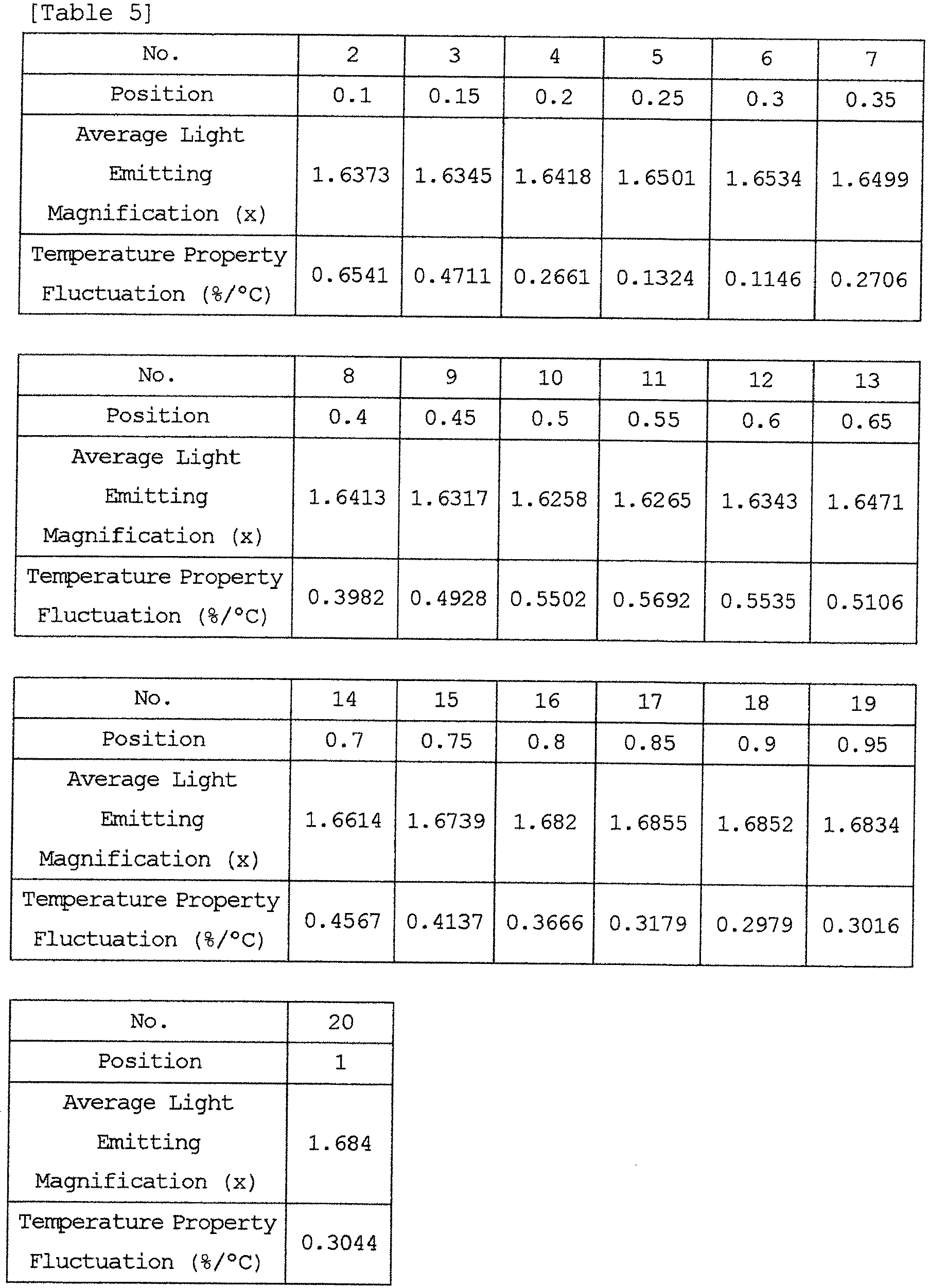
-
Figure 14 illustrates the values of Table 5 as a graph. - It became clear from the present simulation that fluctuations in temperature properties could be decreased to 0.2%/°C or less in an element structure provided with the
upper DBR layer 35 by providing the second phase changing layer within a range from 0.22 to 0.33 when the DBR layer is divided into percentages, with the side thereof toward the light emitting layer designated as 0, and the side thereof toward the substrate designated as 1. - Next, an LED having the layer structure shown in the table of
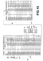
Figure 15 was considered. InSimulation 5, the structure ofSimulation 3 illustrated inFigure 11 , in which the thicknesses of the No. 1 and No. 7 low refractive index layers within thelower DBR layer 30 are λ/2n (=124nm) and are phase changing layers, is employed as a base, and an Al0.3Ga0.7Aslayer 34 is inserted in the No. 7 layer at the central position in the thickness direction thereof, was considered. As schematically shown inFigure 15 , the No. 7 layer is divided into two layers having a thickness of λ/4n (=62nm), and the Al0.3Ga0.7Aslayer 34 is inserted therebetween. The average light emitting magnification and temperature property fluctuations were obtained for cases in which the thickness of the Al0.3Ga0.7Aslayer 34 is varied from 5nm to 80nm in increments of 5nm. The results are shown in Table 6.
- The numerical values of Table 6 are illustrated in
Figure 16 as a graph. - Fluctuations in temperature properties increase as the layer thickness S of the inserted
layer 34 becomes greater. The temperature property fluctuations become greatest in the vicinity of a thickness of 56nm, which is substantially equal to the optical lengths of the layers above and below thelayer 34. Meanwhile, it became clear that the temperature property fluctuations could be decreased to 0.2%/°C or less if the layer thickness S is 15nm or less. That is, even if an inserted layer is provided within the phase changing layer having a thickness of mλ/2n, both the light emission enhancing effect and the temperature property fluctuation suppressing effect can be sufficiently realized, if the thickness of the inserted layer is 15nm or less. - The simulations described above were performed with respect to AlGaAs type semiconductor light emitting elements. However, it is considered that the temperature property fluctuation suppressing effect obtained by providing the phase changing layers within the lower DBR layer will be similarly exhibited regardless of the composition of the semiconductor light emitting element.
- Hereinafter, Examples of the semiconductor light emitting element of the present invention and Comparative Examples will be described.
- Average light intensity fluctuations and temperature property fluctuations were obtained for the Examples and Comparative Examples described below by the simulation technique described above.
- Example 1 is an LED having the layer structure of
Simulation 2 illustrated inFigure 11 , in which the thicknesses t of the No. 1 and No. 7 low refractive index layers are λ/2n. The resonator spectrum of this element obtained by simulations is illustrated inFigure 17 . In addition, the natural light emitting spectrum, the reflectance of the lower DBR layer with respect to the peak light emission wavelength, and the reflectance of the upper AR layer with respect to the peak light emission wavelength are illustrated inFigure 18 . - Example 2 is an LED having the layer structure illustrated in
Figure 19 . In the present element, the thicknesses of the high refractive index layers 32 under the No. 1 and No. 7 low refractive index layers within the lower DBR layer are changed to λ/2n (=116nm) to become phase changing layers. The resonator spectrum of the present element obtained by simulations is illustrated inFigure 20 . - Example 3 is an LED having the layer structure of
Simulation 5 illustrated inFigure 15 , in which the thickness of thelayer 34 inserted into the No. 7 low refractive index layer is 10nm. - Comparative Example 1 is an LED having the layer structure of the
light emitting layer 20 and the layers under thelight emitting layer 20 shown in the table ofFigure 7 , and theupper DBR layer 35 illustrated inFigure 13 as a layer above thelight emitting layer 20. That is, the present element is provided with thelower DBR layer 30 constituted by 19.5 pairs, and theupper DBR layer 35 constituted by 5 pairs, without a phase changing layer having a thickness of mλ/2n. The resonator spectrum of the present element obtained by simulations is illustrated inFigure 21 . - Comparative Example 2 has the layer structure shown in the table of
Figure 7 . That is, the present element is provided with a lower DBR layer constituted by 19.5 pairs, an AR structure as a layer above the light emitting layer instead of a DBR layer, without a phase changing layer having a thickness of mλ/2n. The resonator spectrum of the present element obtained by simulations is illustrated inFigure 22 . - The results of obtaining the average light emitting magnifications and the fluctuations in temperature properties of Examples 1 through 3 as well as Comparative Examples 1 and 2 by the simulation technique described above are shown in Table 7.
[Table 7] Average Light Emitting Magnification M (x) Fluctuation δ of Temperature Properties (%/°C) Example 1 1.603 0.039 Example 2 1.576 0.049 Example 3 1.595 0.127 Comparative Example 1 1.670 0.800 Comparative Example 2 1.605 0.644 - As shown in Table 7, the fluctuations in temperature properties of Example 1 is 1/20 those of a conventional element structure provided with DBR layers above and below a light emitting layer (Comparative Example 1), and exhibits an extremely high temperature property fluctuation suppressing effect. Both of Examples 1 and 2 can suppress temperature property fluctuations to 0.1%/°C or less. This indicates that the layer having the thickness of λ/2n maybe either a low refractive index layer or a high refractive index layer.
- The semiconductor light emitting element of the present invention will exhibit extremely advantageous effects if applied to an LED array exposure device that employs a plurality of LED's produced on a single wafer and has fluctuations in film thicknesses, in which it is necessary to uniformize the light intensities of the plurality of LED's.
Claims (9)
- A semiconductor light emitting element that outputs emitted light having a predetermined emitted light peak wavelength λ, comprising at least:a substrate;a lower distributed Bragg reflector layer provided on the substrate; anda light emitting layer provided on the lower distributed Bragg reflector layer;at least one phase changing layer having a thickness of mλ/2n (wherein n is the refractive index of the phase changing layer, and m is an integer 1 or greater) being provided within the lower distributed Bragg reflector layer.
- A semiconductor light emitting element as defined in Claim 1, wherein:two phase changing layers are provided within the lower distributed Bragg reflector layer.
- A semiconductor light emitting element as defined in either one of Claim 1 and Claim 2, wherein:the lower distributed Bragg reflector layer is basically constituted by two or more pairs of a low refractive index layer having a thickness a and a high refractive index layer having a thickness b which are alternately laminated; andone of the low refractive index layers and the high refractive index layers constituting the phase changing layer having the thickness mλ/2n, which is different from the thickness a and the thickness b.
- A semiconductor light emitting element as defined in any one of Claims 1 through 3, wherein:a distributed Bragg reflector layer is not provided as a layer above the light emitting layer; andan antireflection layer is provided as a layer above the light emitting layer.
- A semiconductor light emitting element as defined in Claim 4, wherein:two of the phase changing layers are provided within the lower distributed Bragg reflector layer;one of the two phase changing layers is one of the low refractive index layer and the high refractive index layer that constitutes the pair most toward the side of the light emitting layer; andthe other of the two phase changing layers is present within one of a range from 0.24 to 0.46 and a range from 0.66 to 0.82, when the lower distributed Bragg reflector layer is divided into percentages, with the side thereof toward the light emitting layer designated as 0, and the side thereof toward the substrate designated as 1.
- A semiconductor light emitting element as defined in Claim 5, wherein the other of the two phase changing layers is present within a range from 0.27 to 0.39 within the lower distributed Bragg reflector layer.
- A semiconductor light emitting element as defined in any one of Claims 1 through 3, further comprising:an upper distributed Bragg reflector layer provided as a layer above the light emitting layer.
- A semiconductor light emitting element as defined in Claim 7, wherein:two of the phase changing layers are provided within the lower distributed Bragg reflector layer;one of the two phase changing layers is one of the low refractive index layer and the high refractive index layer that constitutes the pair most toward the side of the light emitting layer; andthe other of the two phase changing layers is present within one of a range from 0.22 to 0.33, when the lower distributed Bragg reflector layer is divided into percentages, with the side thereof toward the light emitting layer designated as 0, and the side thereof toward the substrate designated as 1.
- A semiconductor light emitting element as defined in any one of Claims 1 through 8, which is a light emitting diode of the surface emitting type.
Applications Claiming Priority (2)
| Application Number | Priority Date | Filing Date | Title |
|---|---|---|---|
| JP2012035076A JP5731996B2 (en) | 2012-02-21 | 2012-02-21 | Semiconductor light emitting device |
| PCT/JP2013/000933 WO2013125214A1 (en) | 2012-02-21 | 2013-02-20 | Semiconductor light-emitting element |
Publications (3)
| Publication Number | Publication Date |
|---|---|
| EP2819182A1 true EP2819182A1 (en) | 2014-12-31 |
| EP2819182A4 EP2819182A4 (en) | 2015-09-23 |
| EP2819182B1 EP2819182B1 (en) | 2017-10-25 |
Family
ID=49005410
Family Applications (1)
| Application Number | Title | Priority Date | Filing Date |
|---|---|---|---|
| EP13751123.4A Not-in-force EP2819182B1 (en) | 2012-02-21 | 2013-02-20 | Semiconductor light-emitting element |
Country Status (4)
| Country | Link |
|---|---|
| US (1) | US9190574B2 (en) |
| EP (1) | EP2819182B1 (en) |
| JP (1) | JP5731996B2 (en) |
| WO (1) | WO2013125214A1 (en) |
Families Citing this family (9)
| Publication number | Priority date | Publication date | Assignee | Title |
|---|---|---|---|---|
| JP6112986B2 (en) | 2013-06-19 | 2017-04-12 | キヤノン株式会社 | Semiconductor DBR, semiconductor light emitting element, solid-state laser, photoacoustic apparatus, image forming apparatus, and method of manufacturing semiconductor DBR |
| JP2015103740A (en) * | 2013-11-27 | 2015-06-04 | キヤノン株式会社 | Surface emitting laser and optical coherence tomography using the same |
| KR102282137B1 (en) * | 2014-11-25 | 2021-07-28 | 삼성전자주식회사 | Semiconductor light emitting device and semiconductor light emitting apparatus having the same |
| KR20160141925A (en) * | 2015-06-01 | 2016-12-12 | 삼성전자주식회사 | Semiconductor light emitting device |
| KR102471102B1 (en) | 2015-10-23 | 2022-11-25 | 서울바이오시스 주식회사 | Light emitting diode chip having distributed bragg reflector |
| CN107919419B (en) * | 2017-09-30 | 2019-11-12 | 华灿光电(浙江)有限公司 | Gallium nitride-based light emitting diode epitaxial wafer and manufacturing method thereof |
| JP6650961B2 (en) * | 2018-04-25 | 2020-02-19 | キヤノン株式会社 | Surface emitting laser and optical coherence tomography using the same |
| TWI842694B (en) * | 2019-01-23 | 2024-05-21 | 晶元光電股份有限公司 | Light-emitting element with distributed bragg reflector |
| JP7455267B1 (en) | 2022-10-28 | 2024-03-25 | Dowaエレクトロニクス株式会社 | Ultraviolet light emitting device and its manufacturing method |
Family Cites Families (14)
| Publication number | Priority date | Publication date | Assignee | Title |
|---|---|---|---|---|
| JPH04333290A (en) * | 1991-05-08 | 1992-11-20 | Nec Corp | Vertical resonator type area emission laser and area input-output photoelectric fusion element |
| US5226053A (en) * | 1991-12-27 | 1993-07-06 | At&T Bell Laboratories | Light emitting diode |
| JPH0793419B2 (en) | 1992-11-04 | 1995-10-09 | 日本電気株式会社 | Light receiving and emitting integrated device |
| JPH07123162B2 (en) * | 1993-01-27 | 1995-12-25 | 日本電気株式会社 | Planar waveguide optical semiconductor device and manufacturing method thereof |
| DE19629920B4 (en) * | 1995-08-10 | 2006-02-02 | LumiLeds Lighting, U.S., LLC, San Jose | Light-emitting diode with a non-absorbing distributed Bragg reflector |
| US6611543B2 (en) * | 2000-12-23 | 2003-08-26 | Applied Optoelectronics, Inc. | Vertical-cavity surface-emitting laser with metal mirror and method of fabrication of same |
| JP4537658B2 (en) * | 2002-02-22 | 2010-09-01 | 株式会社リコー | Surface emitting laser element, surface emitting laser array using the surface emitting laser element, electrophotographic system, surface emitting laser module, optical communication system, optical interconnection system, and surface emitting laser element manufacturing method |
| JP2003332615A (en) | 2002-05-09 | 2003-11-21 | Daido Steel Co Ltd | Semiconductor light emitting device |
| WO2008041138A2 (en) * | 2006-06-16 | 2008-04-10 | Vitaly Shchukin | Coupled cavity ld with tilted wave propagation |
| JP2009070929A (en) | 2007-09-11 | 2009-04-02 | Daido Steel Co Ltd | Surface emitting diode |
| JP4770955B2 (en) | 2009-03-16 | 2011-09-14 | 富士ゼロックス株式会社 | Light emitting device, print head, and image forming apparatus |
| JP2012028667A (en) * | 2010-07-27 | 2012-02-09 | Toshiba Corp | Light emitting device |
| JP5725804B2 (en) * | 2010-11-05 | 2015-05-27 | キヤノン株式会社 | Surface emitting laser and surface emitting laser array, surface emitting laser manufacturing method, surface emitting laser array manufacturing method, and optical apparatus including surface emitting laser array |
| US8624482B2 (en) * | 2011-09-01 | 2014-01-07 | Toshiba Techno Center Inc. | Distributed bragg reflector for reflecting light of multiple wavelengths from an LED |
-
2012
- 2012-02-21 JP JP2012035076A patent/JP5731996B2/en active Active
-
2013
- 2013-02-20 EP EP13751123.4A patent/EP2819182B1/en not_active Not-in-force
- 2013-02-20 WO PCT/JP2013/000933 patent/WO2013125214A1/en not_active Ceased
-
2014
- 2014-08-21 US US14/465,354 patent/US9190574B2/en not_active Expired - Fee Related
Also Published As
| Publication number | Publication date |
|---|---|
| US9190574B2 (en) | 2015-11-17 |
| WO2013125214A1 (en) | 2013-08-29 |
| US20140361330A1 (en) | 2014-12-11 |
| EP2819182A4 (en) | 2015-09-23 |
| JP2013171992A (en) | 2013-09-02 |
| EP2819182B1 (en) | 2017-10-25 |
| JP5731996B2 (en) | 2015-06-10 |
Similar Documents
| Publication | Publication Date | Title |
|---|---|---|
| EP2819182B1 (en) | Semiconductor light-emitting element | |
| EP2579071B1 (en) | Echelle diffraction grating, excimer laser, manufacturing method of echelle diffraction grating, and ArF excimer laser | |
| KR101760937B1 (en) | Vertical cavity surface emitting laser | |
| WO2021108017A1 (en) | Top emitting vcsel array with integrated gratings | |
| US20180175590A1 (en) | Semiconductor laser device | |
| JP6066634B2 (en) | Method for manufacturing echelle diffraction grating and method for manufacturing excimer laser | |
| KR101098724B1 (en) | Multiple wavelength semiconductor laser and manufacturing method thereof | |
| US20110142090A1 (en) | Laser diode and method of manufacturing laser diode | |
| US20200036162A1 (en) | Laser | |
| WO2010147035A1 (en) | Semiconductor laser and optical module using same | |
| JP2009070929A (en) | Surface emitting diode | |
| JP5728411B2 (en) | Semiconductor light emitting device | |
| JP2008294090A (en) | Semiconductor laser element | |
| KR20240123589A (en) | High reflectance multilayer structure and method of manufacturing the same | |
| KR20140127034A (en) | Edge emitting laser diode and method for manufacturing the same | |
| JP5787069B2 (en) | Multi-wavelength semiconductor laser device | |
| US20150139261A1 (en) | Semiconductor device having a semiconductor dbr layer | |
| KR20060132483A (en) | Multiwavelength Laser Diode | |
| JP2009070928A (en) | Surface emitting diode | |
| JP2010165723A (en) | Method of manufacturing surface emitting laser | |
| JP6804188B2 (en) | Semiconductor multilayer reflector | |
| US20240380186A1 (en) | Semiconductor laser element | |
| EP4492592A1 (en) | Semiconductor light-emitting element and external resonator type laser module | |
| US20070280307A1 (en) | Semiconductor laser device | |
| JP2778868B2 (en) | Surface-emitting light emitting diode |
Legal Events
| Date | Code | Title | Description |
|---|---|---|---|
| PUAI | Public reference made under article 153(3) epc to a published international application that has entered the european phase |
Free format text: ORIGINAL CODE: 0009012 |
|
| 17P | Request for examination filed |
Effective date: 20140908 |
|
| AK | Designated contracting states |
Kind code of ref document: A1 Designated state(s): AL AT BE BG CH CY CZ DE DK EE ES FI FR GB GR HR HU IE IS IT LI LT LU LV MC MK MT NL NO PL PT RO RS SE SI SK SM TR |
|
| AX | Request for extension of the european patent |
Extension state: BA ME |
|
| DAX | Request for extension of the european patent (deleted) | ||
| RA4 | Supplementary search report drawn up and despatched (corrected) |
Effective date: 20150825 |
|
| RIC1 | Information provided on ipc code assigned before grant |
Ipc: H01L 33/10 20100101AFI20150819BHEP Ipc: H01L 33/30 20100101ALI20150819BHEP |
|
| 17Q | First examination report despatched |
Effective date: 20161006 |
|
| REG | Reference to a national code |
Ref country code: DE Ref legal event code: R079 Ref document number: 602013028419 Country of ref document: DE Free format text: PREVIOUS MAIN CLASS: H01L0033100000 Ipc: H01S0005125000 |
|
| RIC1 | Information provided on ipc code assigned before grant |
Ipc: H01L 33/30 20100101ALI20170428BHEP Ipc: H01L 33/10 20100101ALI20170428BHEP Ipc: H01S 5/125 20060101AFI20170428BHEP Ipc: H01S 5/00 20060101ALI20170428BHEP Ipc: H01S 5/187 20060101ALI20170428BHEP |
|
| GRAP | Despatch of communication of intention to grant a patent |
Free format text: ORIGINAL CODE: EPIDOSNIGR1 |
|
| INTG | Intention to grant announced |
Effective date: 20170609 |
|
| RIN1 | Information on inventor provided before grant (corrected) |
Inventor name: HAKUTA, SHINYA |
|
| GRAS | Grant fee paid |
Free format text: ORIGINAL CODE: EPIDOSNIGR3 |
|
| GRAA | (expected) grant |
Free format text: ORIGINAL CODE: 0009210 |
|
| AK | Designated contracting states |
Kind code of ref document: B1 Designated state(s): AL AT BE BG CH CY CZ DE DK EE ES FI FR GB GR HR HU IE IS IT LI LT LU LV MC MK MT NL NO PL PT RO RS SE SI SK SM TR |
|
| REG | Reference to a national code |
Ref country code: GB Ref legal event code: FG4D |
|
| REG | Reference to a national code |
Ref country code: CH Ref legal event code: EP |
|
| REG | Reference to a national code |
Ref country code: AT Ref legal event code: REF Ref document number: 940733 Country of ref document: AT Kind code of ref document: T Effective date: 20171115 |
|
| REG | Reference to a national code |
Ref country code: IE Ref legal event code: FG4D |
|
| REG | Reference to a national code |
Ref country code: DE Ref legal event code: R096 Ref document number: 602013028419 Country of ref document: DE |
|
| REG | Reference to a national code |
Ref country code: NL Ref legal event code: MP Effective date: 20171025 |
|
| REG | Reference to a national code |
Ref country code: LT Ref legal event code: MG4D |
|
| REG | Reference to a national code |
Ref country code: AT Ref legal event code: MK05 Ref document number: 940733 Country of ref document: AT Kind code of ref document: T Effective date: 20171025 |
|
| PG25 | Lapsed in a contracting state [announced via postgrant information from national office to epo] |
Ref country code: NL Free format text: LAPSE BECAUSE OF FAILURE TO SUBMIT A TRANSLATION OF THE DESCRIPTION OR TO PAY THE FEE WITHIN THE PRESCRIBED TIME-LIMIT Effective date: 20171025 |
|
| PG25 | Lapsed in a contracting state [announced via postgrant information from national office to epo] |
Ref country code: ES Free format text: LAPSE BECAUSE OF FAILURE TO SUBMIT A TRANSLATION OF THE DESCRIPTION OR TO PAY THE FEE WITHIN THE PRESCRIBED TIME-LIMIT Effective date: 20171025 Ref country code: SE Free format text: LAPSE BECAUSE OF FAILURE TO SUBMIT A TRANSLATION OF THE DESCRIPTION OR TO PAY THE FEE WITHIN THE PRESCRIBED TIME-LIMIT Effective date: 20171025 Ref country code: NO Free format text: LAPSE BECAUSE OF FAILURE TO SUBMIT A TRANSLATION OF THE DESCRIPTION OR TO PAY THE FEE WITHIN THE PRESCRIBED TIME-LIMIT Effective date: 20180125 Ref country code: LT Free format text: LAPSE BECAUSE OF FAILURE TO SUBMIT A TRANSLATION OF THE DESCRIPTION OR TO PAY THE FEE WITHIN THE PRESCRIBED TIME-LIMIT Effective date: 20171025 Ref country code: FI Free format text: LAPSE BECAUSE OF FAILURE TO SUBMIT A TRANSLATION OF THE DESCRIPTION OR TO PAY THE FEE WITHIN THE PRESCRIBED TIME-LIMIT Effective date: 20171025 |
|
| PG25 | Lapsed in a contracting state [announced via postgrant information from national office to epo] |
Ref country code: IS Free format text: LAPSE BECAUSE OF FAILURE TO SUBMIT A TRANSLATION OF THE DESCRIPTION OR TO PAY THE FEE WITHIN THE PRESCRIBED TIME-LIMIT Effective date: 20180225 Ref country code: LV Free format text: LAPSE BECAUSE OF FAILURE TO SUBMIT A TRANSLATION OF THE DESCRIPTION OR TO PAY THE FEE WITHIN THE PRESCRIBED TIME-LIMIT Effective date: 20171025 Ref country code: HR Free format text: LAPSE BECAUSE OF FAILURE TO SUBMIT A TRANSLATION OF THE DESCRIPTION OR TO PAY THE FEE WITHIN THE PRESCRIBED TIME-LIMIT Effective date: 20171025 Ref country code: GR Free format text: LAPSE BECAUSE OF FAILURE TO SUBMIT A TRANSLATION OF THE DESCRIPTION OR TO PAY THE FEE WITHIN THE PRESCRIBED TIME-LIMIT Effective date: 20180126 Ref country code: BG Free format text: LAPSE BECAUSE OF FAILURE TO SUBMIT A TRANSLATION OF THE DESCRIPTION OR TO PAY THE FEE WITHIN THE PRESCRIBED TIME-LIMIT Effective date: 20180125 Ref country code: RS Free format text: LAPSE BECAUSE OF FAILURE TO SUBMIT A TRANSLATION OF THE DESCRIPTION OR TO PAY THE FEE WITHIN THE PRESCRIBED TIME-LIMIT Effective date: 20171025 Ref country code: AT Free format text: LAPSE BECAUSE OF FAILURE TO SUBMIT A TRANSLATION OF THE DESCRIPTION OR TO PAY THE FEE WITHIN THE PRESCRIBED TIME-LIMIT Effective date: 20171025 |
|
| REG | Reference to a national code |
Ref country code: DE Ref legal event code: R097 Ref document number: 602013028419 Country of ref document: DE |
|
| PG25 | Lapsed in a contracting state [announced via postgrant information from national office to epo] |
Ref country code: SK Free format text: LAPSE BECAUSE OF FAILURE TO SUBMIT A TRANSLATION OF THE DESCRIPTION OR TO PAY THE FEE WITHIN THE PRESCRIBED TIME-LIMIT Effective date: 20171025 Ref country code: CZ Free format text: LAPSE BECAUSE OF FAILURE TO SUBMIT A TRANSLATION OF THE DESCRIPTION OR TO PAY THE FEE WITHIN THE PRESCRIBED TIME-LIMIT Effective date: 20171025 Ref country code: EE Free format text: LAPSE BECAUSE OF FAILURE TO SUBMIT A TRANSLATION OF THE DESCRIPTION OR TO PAY THE FEE WITHIN THE PRESCRIBED TIME-LIMIT Effective date: 20171025 Ref country code: DK Free format text: LAPSE BECAUSE OF FAILURE TO SUBMIT A TRANSLATION OF THE DESCRIPTION OR TO PAY THE FEE WITHIN THE PRESCRIBED TIME-LIMIT Effective date: 20171025 Ref country code: CY Free format text: LAPSE BECAUSE OF FAILURE TO SUBMIT A TRANSLATION OF THE DESCRIPTION OR TO PAY THE FEE WITHIN THE PRESCRIBED TIME-LIMIT Effective date: 20171025 |
|
| PG25 | Lapsed in a contracting state [announced via postgrant information from national office to epo] |
Ref country code: RO Free format text: LAPSE BECAUSE OF FAILURE TO SUBMIT A TRANSLATION OF THE DESCRIPTION OR TO PAY THE FEE WITHIN THE PRESCRIBED TIME-LIMIT Effective date: 20171025 Ref country code: IT Free format text: LAPSE BECAUSE OF FAILURE TO SUBMIT A TRANSLATION OF THE DESCRIPTION OR TO PAY THE FEE WITHIN THE PRESCRIBED TIME-LIMIT Effective date: 20171025 Ref country code: SM Free format text: LAPSE BECAUSE OF FAILURE TO SUBMIT A TRANSLATION OF THE DESCRIPTION OR TO PAY THE FEE WITHIN THE PRESCRIBED TIME-LIMIT Effective date: 20171025 Ref country code: PL Free format text: LAPSE BECAUSE OF FAILURE TO SUBMIT A TRANSLATION OF THE DESCRIPTION OR TO PAY THE FEE WITHIN THE PRESCRIBED TIME-LIMIT Effective date: 20171025 |
|
| PLBE | No opposition filed within time limit |
Free format text: ORIGINAL CODE: 0009261 |
|
| STAA | Information on the status of an ep patent application or granted ep patent |
Free format text: STATUS: NO OPPOSITION FILED WITHIN TIME LIMIT |
|
| REG | Reference to a national code |
Ref country code: CH Ref legal event code: PL |
|
| PG25 | Lapsed in a contracting state [announced via postgrant information from national office to epo] |
Ref country code: MC Free format text: LAPSE BECAUSE OF FAILURE TO SUBMIT A TRANSLATION OF THE DESCRIPTION OR TO PAY THE FEE WITHIN THE PRESCRIBED TIME-LIMIT Effective date: 20171025 |
|
| 26N | No opposition filed |
Effective date: 20180726 |
|
| REG | Reference to a national code |
Ref country code: IE Ref legal event code: MM4A |
|
| REG | Reference to a national code |
Ref country code: BE Ref legal event code: MM Effective date: 20180228 |
|
| PG25 | Lapsed in a contracting state [announced via postgrant information from national office to epo] |
Ref country code: SI Free format text: LAPSE BECAUSE OF FAILURE TO SUBMIT A TRANSLATION OF THE DESCRIPTION OR TO PAY THE FEE WITHIN THE PRESCRIBED TIME-LIMIT Effective date: 20171025 Ref country code: CH Free format text: LAPSE BECAUSE OF NON-PAYMENT OF DUE FEES Effective date: 20180228 Ref country code: LI Free format text: LAPSE BECAUSE OF NON-PAYMENT OF DUE FEES Effective date: 20180228 Ref country code: LU Free format text: LAPSE BECAUSE OF NON-PAYMENT OF DUE FEES Effective date: 20180220 |
|
| REG | Reference to a national code |
Ref country code: FR Ref legal event code: ST Effective date: 20181031 |
|
| PG25 | Lapsed in a contracting state [announced via postgrant information from national office to epo] |
Ref country code: IE Free format text: LAPSE BECAUSE OF NON-PAYMENT OF DUE FEES Effective date: 20180220 |
|
| PG25 | Lapsed in a contracting state [announced via postgrant information from national office to epo] |
Ref country code: BE Free format text: LAPSE BECAUSE OF NON-PAYMENT OF DUE FEES Effective date: 20180228 Ref country code: FR Free format text: LAPSE BECAUSE OF NON-PAYMENT OF DUE FEES Effective date: 20180228 |
|
| PGFP | Annual fee paid to national office [announced via postgrant information from national office to epo] |
Ref country code: GB Payment date: 20190220 Year of fee payment: 7 |
|
| PG25 | Lapsed in a contracting state [announced via postgrant information from national office to epo] |
Ref country code: MT Free format text: LAPSE BECAUSE OF NON-PAYMENT OF DUE FEES Effective date: 20180220 |
|
| PG25 | Lapsed in a contracting state [announced via postgrant information from national office to epo] |
Ref country code: TR Free format text: LAPSE BECAUSE OF FAILURE TO SUBMIT A TRANSLATION OF THE DESCRIPTION OR TO PAY THE FEE WITHIN THE PRESCRIBED TIME-LIMIT Effective date: 20171025 |
|
| PGFP | Annual fee paid to national office [announced via postgrant information from national office to epo] |
Ref country code: DE Payment date: 20200204 Year of fee payment: 8 |
|
| PG25 | Lapsed in a contracting state [announced via postgrant information from national office to epo] |
Ref country code: HU Free format text: LAPSE BECAUSE OF FAILURE TO SUBMIT A TRANSLATION OF THE DESCRIPTION OR TO PAY THE FEE WITHIN THE PRESCRIBED TIME-LIMIT; INVALID AB INITIO Effective date: 20130220 Ref country code: PT Free format text: LAPSE BECAUSE OF FAILURE TO SUBMIT A TRANSLATION OF THE DESCRIPTION OR TO PAY THE FEE WITHIN THE PRESCRIBED TIME-LIMIT Effective date: 20171025 |
|
| PG25 | Lapsed in a contracting state [announced via postgrant information from national office to epo] |
Ref country code: MK Free format text: LAPSE BECAUSE OF NON-PAYMENT OF DUE FEES Effective date: 20171025 |
|
| PG25 | Lapsed in a contracting state [announced via postgrant information from national office to epo] |
Ref country code: AL Free format text: LAPSE BECAUSE OF FAILURE TO SUBMIT A TRANSLATION OF THE DESCRIPTION OR TO PAY THE FEE WITHIN THE PRESCRIBED TIME-LIMIT Effective date: 20171025 |
|
| GBPC | Gb: european patent ceased through non-payment of renewal fee |
Effective date: 20200220 |
|
| PG25 | Lapsed in a contracting state [announced via postgrant information from national office to epo] |
Ref country code: GB Free format text: LAPSE BECAUSE OF NON-PAYMENT OF DUE FEES Effective date: 20200220 |
|
| REG | Reference to a national code |
Ref country code: DE Ref legal event code: R119 Ref document number: 602013028419 Country of ref document: DE |
|
| PG25 | Lapsed in a contracting state [announced via postgrant information from national office to epo] |
Ref country code: DE Free format text: LAPSE BECAUSE OF NON-PAYMENT OF DUE FEES Effective date: 20210901 |