EP2818849A1 - Fluorescent sensor and sensor system - Google Patents
Fluorescent sensor and sensor system Download PDFInfo
- Publication number
- EP2818849A1 EP2818849A1 EP13748980.3A EP13748980A EP2818849A1 EP 2818849 A1 EP2818849 A1 EP 2818849A1 EP 13748980 A EP13748980 A EP 13748980A EP 2818849 A1 EP2818849 A1 EP 2818849A1
- Authority
- EP
- European Patent Office
- Prior art keywords
- hole
- main surface
- photoelectric conversion
- sensor
- conversion element
- Prior art date
- Legal status (The legal status is an assumption and is not a legal conclusion. Google has not performed a legal analysis and makes no representation as to the accuracy of the status listed.)
- Withdrawn
Links
- 230000005284 excitation Effects 0.000 claims abstract description 40
- 239000012491 analyte Substances 0.000 claims abstract description 38
- 239000000758 substrate Substances 0.000 claims abstract description 34
- 230000000903 blocking effect Effects 0.000 claims abstract description 27
- 238000006243 chemical reaction Methods 0.000 claims description 30
- 238000001514 detection method Methods 0.000 claims description 30
- 239000010410 layer Substances 0.000 description 98
- 238000000034 method Methods 0.000 description 23
- XUIMIQQOPSSXEZ-UHFFFAOYSA-N Silicon Chemical compound [Si] XUIMIQQOPSSXEZ-UHFFFAOYSA-N 0.000 description 21
- 229910052710 silicon Inorganic materials 0.000 description 20
- 239000007850 fluorescent dye Substances 0.000 description 19
- 239000000463 material Substances 0.000 description 19
- 239000010703 silicon Substances 0.000 description 19
- 238000004519 manufacturing process Methods 0.000 description 16
- 229920005989 resin Polymers 0.000 description 10
- 239000011347 resin Substances 0.000 description 10
- 239000012535 impurity Substances 0.000 description 9
- 230000008569 process Effects 0.000 description 9
- 239000011241 protective layer Substances 0.000 description 9
- 238000009413 insulation Methods 0.000 description 8
- 239000000243 solution Substances 0.000 description 8
- VYPSYNLAJGMNEJ-UHFFFAOYSA-N Silicium dioxide Chemical compound O=[Si]=O VYPSYNLAJGMNEJ-UHFFFAOYSA-N 0.000 description 7
- 230000005540 biological transmission Effects 0.000 description 7
- 239000000017 hydrogel Substances 0.000 description 7
- 230000035945 sensitivity Effects 0.000 description 7
- 239000011229 interlayer Substances 0.000 description 6
- 239000004065 semiconductor Substances 0.000 description 6
- 229910052581 Si3N4 Inorganic materials 0.000 description 5
- HQVNEWCFYHHQES-UHFFFAOYSA-N silicon nitride Chemical compound N12[Si]34N5[Si]62N3[Si]51N64 HQVNEWCFYHHQES-UHFFFAOYSA-N 0.000 description 5
- 229910052814 silicon oxide Inorganic materials 0.000 description 5
- 230000015572 biosynthetic process Effects 0.000 description 4
- 230000000694 effects Effects 0.000 description 4
- 238000005516 engineering process Methods 0.000 description 4
- 238000005530 etching Methods 0.000 description 4
- 230000006870 function Effects 0.000 description 4
- 239000002356 single layer Substances 0.000 description 4
- WGTYBPLFGIVFAS-UHFFFAOYSA-M tetramethylammonium hydroxide Chemical compound [OH-].C[N+](C)(C)C WGTYBPLFGIVFAS-UHFFFAOYSA-M 0.000 description 4
- WQZGKKKJIJFFOK-GASJEMHNSA-N Glucose Natural products OC[C@H]1OC(O)[C@H](O)[C@@H](O)[C@@H]1O WQZGKKKJIJFFOK-GASJEMHNSA-N 0.000 description 3
- 229910052782 aluminium Inorganic materials 0.000 description 3
- 239000006229 carbon black Substances 0.000 description 3
- 238000005229 chemical vapour deposition Methods 0.000 description 3
- 239000000499 gel Substances 0.000 description 3
- 239000008103 glucose Substances 0.000 description 3
- 238000010030 laminating Methods 0.000 description 3
- 238000005259 measurement Methods 0.000 description 3
- 230000035699 permeability Effects 0.000 description 3
- 230000000379 polymerizing effect Effects 0.000 description 3
- 235000000346 sugar Nutrition 0.000 description 3
- 150000008163 sugars Chemical class 0.000 description 3
- HRPVXLWXLXDGHG-UHFFFAOYSA-N Acrylamide Chemical compound NC(=O)C=C HRPVXLWXLXDGHG-UHFFFAOYSA-N 0.000 description 2
- ZOXJGFHDIHLPTG-UHFFFAOYSA-N Boron Chemical compound [B] ZOXJGFHDIHLPTG-UHFFFAOYSA-N 0.000 description 2
- CURLTUGMZLYLDI-UHFFFAOYSA-N Carbon dioxide Chemical compound O=C=O CURLTUGMZLYLDI-UHFFFAOYSA-N 0.000 description 2
- 239000004642 Polyimide Substances 0.000 description 2
- XAGFODPZIPBFFR-UHFFFAOYSA-N aluminium Chemical compound [Al] XAGFODPZIPBFFR-UHFFFAOYSA-N 0.000 description 2
- 210000001124 body fluid Anatomy 0.000 description 2
- 229910052796 boron Inorganic materials 0.000 description 2
- 239000000919 ceramic Substances 0.000 description 2
- 239000012530 fluid Substances 0.000 description 2
- 239000011521 glass Substances 0.000 description 2
- -1 glucose Chemical class 0.000 description 2
- 238000010438 heat treatment Methods 0.000 description 2
- 239000012774 insulation material Substances 0.000 description 2
- 238000005468 ion implantation Methods 0.000 description 2
- 239000007788 liquid Substances 0.000 description 2
- 150000004767 nitrides Chemical class 0.000 description 2
- HXITXNWTGFUOAU-UHFFFAOYSA-N phenylboronic acid Chemical class OB(O)C1=CC=CC=C1 HXITXNWTGFUOAU-UHFFFAOYSA-N 0.000 description 2
- 229910021420 polycrystalline silicon Inorganic materials 0.000 description 2
- 229920001721 polyimide Polymers 0.000 description 2
- 239000003505 polymerization initiator Substances 0.000 description 2
- 229920005591 polysilicon Polymers 0.000 description 2
- HBMJWWWQQXIZIP-UHFFFAOYSA-N silicon carbide Chemical compound [Si+]#[C-] HBMJWWWQQXIZIP-UHFFFAOYSA-N 0.000 description 2
- 229910010271 silicon carbide Inorganic materials 0.000 description 2
- 229920002050 silicone resin Polymers 0.000 description 2
- CHQMHPLRPQMAMX-UHFFFAOYSA-L sodium persulfate Chemical compound [Na+].[Na+].[O-]S(=O)(=O)OOS([O-])(=O)=O CHQMHPLRPQMAMX-UHFFFAOYSA-L 0.000 description 2
- OMIGHNLMNHATMP-UHFFFAOYSA-N 2-hydroxyethyl prop-2-enoate Chemical compound OCCOC(=O)C=C OMIGHNLMNHATMP-UHFFFAOYSA-N 0.000 description 1
- MTYHUTYJKFVTJJ-UHFFFAOYSA-N 4-hydroxypyrene-1,2,3-trisulfonic acid Chemical class OS(=O)(=O)C1=C(S(O)(=O)=O)C(S(O)(=O)=O)=C2C(O)=CC3=CC=CC4=CC=C1C2=C34 MTYHUTYJKFVTJJ-UHFFFAOYSA-N 0.000 description 1
- NIXOWILDQLNWCW-UHFFFAOYSA-M Acrylate Chemical compound [O-]C(=O)C=C NIXOWILDQLNWCW-UHFFFAOYSA-M 0.000 description 1
- OKTJSMMVPCPJKN-UHFFFAOYSA-N Carbon Chemical compound [C] OKTJSMMVPCPJKN-UHFFFAOYSA-N 0.000 description 1
- 229920002307 Dextran Polymers 0.000 description 1
- 102000004190 Enzymes Human genes 0.000 description 1
- 108090000790 Enzymes Proteins 0.000 description 1
- JOYRKODLDBILNP-UHFFFAOYSA-N Ethyl urethane Chemical compound CCOC(N)=O JOYRKODLDBILNP-UHFFFAOYSA-N 0.000 description 1
- 241000446313 Lamella Species 0.000 description 1
- KWYHDKDOAIKMQN-UHFFFAOYSA-N N,N,N',N'-tetramethylethylenediamine Chemical compound CN(C)CCN(C)C KWYHDKDOAIKMQN-UHFFFAOYSA-N 0.000 description 1
- 239000004698 Polyethylene Substances 0.000 description 1
- 239000002202 Polyethylene glycol Substances 0.000 description 1
- KWYUFKZDYYNOTN-UHFFFAOYSA-M Potassium hydroxide Chemical compound [OH-].[K+] KWYUFKZDYYNOTN-UHFFFAOYSA-M 0.000 description 1
- NPYPAHLBTDXSSS-UHFFFAOYSA-N Potassium ion Chemical compound [K+] NPYPAHLBTDXSSS-UHFFFAOYSA-N 0.000 description 1
- KJTLSVCANCCWHF-UHFFFAOYSA-N Ruthenium Chemical compound [Ru] KJTLSVCANCCWHF-UHFFFAOYSA-N 0.000 description 1
- 239000006087 Silane Coupling Agent Substances 0.000 description 1
- 238000010521 absorption reaction Methods 0.000 description 1
- 125000003647 acryloyl group Chemical group O=C([*])C([H])=C([H])[H] 0.000 description 1
- 239000000853 adhesive Substances 0.000 description 1
- 230000001070 adhesive effect Effects 0.000 description 1
- 239000012790 adhesive layer Substances 0.000 description 1
- 229910052785 arsenic Inorganic materials 0.000 description 1
- RQNWIZPPADIBDY-UHFFFAOYSA-N arsenic atom Chemical compound [As] RQNWIZPPADIBDY-UHFFFAOYSA-N 0.000 description 1
- 230000004888 barrier function Effects 0.000 description 1
- 230000008901 benefit Effects 0.000 description 1
- 125000001797 benzyl group Chemical group [H]C1=C([H])C([H])=C(C([H])=C1[H])C([H])([H])* 0.000 description 1
- 229910052799 carbon Inorganic materials 0.000 description 1
- 239000001569 carbon dioxide Substances 0.000 description 1
- 229910002092 carbon dioxide Inorganic materials 0.000 description 1
- 125000006297 carbonyl amino group Chemical group [H]N([*:2])C([*:1])=O 0.000 description 1
- 229920002678 cellulose Polymers 0.000 description 1
- 235000010980 cellulose Nutrition 0.000 description 1
- 229910052681 coesite Inorganic materials 0.000 description 1
- 239000002131 composite material Substances 0.000 description 1
- 150000001875 compounds Chemical class 0.000 description 1
- 229910052802 copper Inorganic materials 0.000 description 1
- 229910052906 cristobalite Inorganic materials 0.000 description 1
- 150000003983 crown ethers Chemical class 0.000 description 1
- 230000007423 decrease Effects 0.000 description 1
- 125000005442 diisocyanate group Chemical group 0.000 description 1
- 239000006185 dispersion Substances 0.000 description 1
- 239000003822 epoxy resin Substances 0.000 description 1
- GNBHRKFJIUUOQI-UHFFFAOYSA-N fluorescein Chemical compound O1C(=O)C2=CC=CC=C2C21C1=CC=C(O)C=C1OC1=CC(O)=CC=C21 GNBHRKFJIUUOQI-UHFFFAOYSA-N 0.000 description 1
- 150000004676 glycans Chemical class 0.000 description 1
- 229910052737 gold Inorganic materials 0.000 description 1
- BHEPBYXIRTUNPN-UHFFFAOYSA-N hydridophosphorus(.) (triplet) Chemical compound [PH] BHEPBYXIRTUNPN-UHFFFAOYSA-N 0.000 description 1
- GPRLSGONYQIRFK-UHFFFAOYSA-N hydron Chemical compound [H+] GPRLSGONYQIRFK-UHFFFAOYSA-N 0.000 description 1
- 238000002513 implantation Methods 0.000 description 1
- 238000001727 in vivo Methods 0.000 description 1
- 229910010272 inorganic material Inorganic materials 0.000 description 1
- 239000011147 inorganic material Substances 0.000 description 1
- 230000003993 interaction Effects 0.000 description 1
- 230000001678 irradiating effect Effects 0.000 description 1
- 229910052751 metal Inorganic materials 0.000 description 1
- 239000002184 metal Substances 0.000 description 1
- 239000007769 metal material Substances 0.000 description 1
- 150000002739 metals Chemical class 0.000 description 1
- FQPSGWSUVKBHSU-UHFFFAOYSA-N methacrylamide Chemical compound CC(=C)C(N)=O FQPSGWSUVKBHSU-UHFFFAOYSA-N 0.000 description 1
- 229920000609 methyl cellulose Polymers 0.000 description 1
- 125000002496 methyl group Chemical group [H]C([H])([H])* 0.000 description 1
- 239000001923 methylcellulose Substances 0.000 description 1
- 244000005700 microbiome Species 0.000 description 1
- 229910021421 monocrystalline silicon Inorganic materials 0.000 description 1
- 239000000178 monomer Substances 0.000 description 1
- 239000012299 nitrogen atmosphere Substances 0.000 description 1
- 239000011368 organic material Substances 0.000 description 1
- 229920000620 organic polymer Polymers 0.000 description 1
- 239000008055 phosphate buffer solution Substances 0.000 description 1
- 229910052697 platinum Inorganic materials 0.000 description 1
- 229920002401 polyacrylamide Polymers 0.000 description 1
- 229920000647 polyepoxide Polymers 0.000 description 1
- 229920000573 polyethylene Polymers 0.000 description 1
- 229920001223 polyethylene glycol Polymers 0.000 description 1
- 229920000642 polymer Polymers 0.000 description 1
- 229920001282 polysaccharide Polymers 0.000 description 1
- 239000005017 polysaccharide Substances 0.000 description 1
- 229920002635 polyurethane Polymers 0.000 description 1
- 239000004814 polyurethane Substances 0.000 description 1
- 229910001414 potassium ion Inorganic materials 0.000 description 1
- 102000004169 proteins and genes Human genes 0.000 description 1
- 108090000623 proteins and genes Proteins 0.000 description 1
- 229910052707 ruthenium Inorganic materials 0.000 description 1
- 238000007789 sealing Methods 0.000 description 1
- 239000000377 silicon dioxide Substances 0.000 description 1
- 239000002210 silicon-based material Substances 0.000 description 1
- 229910052709 silver Inorganic materials 0.000 description 1
- 239000004332 silver Substances 0.000 description 1
- 238000004544 sputter deposition Methods 0.000 description 1
- 229910052682 stishovite Inorganic materials 0.000 description 1
- 239000012780 transparent material Substances 0.000 description 1
- 229910052905 tridymite Inorganic materials 0.000 description 1
- 229910052721 tungsten Inorganic materials 0.000 description 1
- 238000007740 vapor deposition Methods 0.000 description 1
- 238000001039 wet etching Methods 0.000 description 1
Images




Classifications
-
- G—PHYSICS
- G01—MEASURING; TESTING
- G01N—INVESTIGATING OR ANALYSING MATERIALS BY DETERMINING THEIR CHEMICAL OR PHYSICAL PROPERTIES
- G01N21/00—Investigating or analysing materials by the use of optical means, i.e. using sub-millimetre waves, infrared, visible or ultraviolet light
- G01N21/62—Systems in which the material investigated is excited whereby it emits light or causes a change in wavelength of the incident light
- G01N21/63—Systems in which the material investigated is excited whereby it emits light or causes a change in wavelength of the incident light optically excited
- G01N21/64—Fluorescence; Phosphorescence
- G01N21/6428—Measuring fluorescence of fluorescent products of reactions or of fluorochrome labelled reactive substances, e.g. measuring quenching effects, using measuring "optrodes"
-
- G—PHYSICS
- G01—MEASURING; TESTING
- G01N—INVESTIGATING OR ANALYSING MATERIALS BY DETERMINING THEIR CHEMICAL OR PHYSICAL PROPERTIES
- G01N21/00—Investigating or analysing materials by the use of optical means, i.e. using sub-millimetre waves, infrared, visible or ultraviolet light
- G01N21/62—Systems in which the material investigated is excited whereby it emits light or causes a change in wavelength of the incident light
- G01N21/63—Systems in which the material investigated is excited whereby it emits light or causes a change in wavelength of the incident light optically excited
- G01N21/64—Fluorescence; Phosphorescence
- G01N21/645—Specially adapted constructive features of fluorimeters
-
- G—PHYSICS
- G01—MEASURING; TESTING
- G01N—INVESTIGATING OR ANALYSING MATERIALS BY DETERMINING THEIR CHEMICAL OR PHYSICAL PROPERTIES
- G01N21/00—Investigating or analysing materials by the use of optical means, i.e. using sub-millimetre waves, infrared, visible or ultraviolet light
- G01N21/75—Systems in which material is subjected to a chemical reaction, the progress or the result of the reaction being investigated
- G01N21/77—Systems in which material is subjected to a chemical reaction, the progress or the result of the reaction being investigated by observing the effect on a chemical indicator
-
- G—PHYSICS
- G01—MEASURING; TESTING
- G01N—INVESTIGATING OR ANALYSING MATERIALS BY DETERMINING THEIR CHEMICAL OR PHYSICAL PROPERTIES
- G01N21/00—Investigating or analysing materials by the use of optical means, i.e. using sub-millimetre waves, infrared, visible or ultraviolet light
- G01N21/62—Systems in which the material investigated is excited whereby it emits light or causes a change in wavelength of the incident light
- G01N21/63—Systems in which the material investigated is excited whereby it emits light or causes a change in wavelength of the incident light optically excited
- G01N21/64—Fluorescence; Phosphorescence
- G01N21/6428—Measuring fluorescence of fluorescent products of reactions or of fluorochrome labelled reactive substances, e.g. measuring quenching effects, using measuring "optrodes"
- G01N2021/6434—Optrodes
-
- G—PHYSICS
- G01—MEASURING; TESTING
- G01N—INVESTIGATING OR ANALYSING MATERIALS BY DETERMINING THEIR CHEMICAL OR PHYSICAL PROPERTIES
- G01N21/00—Investigating or analysing materials by the use of optical means, i.e. using sub-millimetre waves, infrared, visible or ultraviolet light
- G01N21/62—Systems in which the material investigated is excited whereby it emits light or causes a change in wavelength of the incident light
- G01N21/63—Systems in which the material investigated is excited whereby it emits light or causes a change in wavelength of the incident light optically excited
- G01N21/64—Fluorescence; Phosphorescence
- G01N21/645—Specially adapted constructive features of fluorimeters
- G01N2021/6463—Optics
- G01N2021/6469—Cavity, e.g. ellipsoid
-
- G—PHYSICS
- G01—MEASURING; TESTING
- G01N—INVESTIGATING OR ANALYSING MATERIALS BY DETERMINING THEIR CHEMICAL OR PHYSICAL PROPERTIES
- G01N21/00—Investigating or analysing materials by the use of optical means, i.e. using sub-millimetre waves, infrared, visible or ultraviolet light
- G01N21/62—Systems in which the material investigated is excited whereby it emits light or causes a change in wavelength of the incident light
- G01N21/63—Systems in which the material investigated is excited whereby it emits light or causes a change in wavelength of the incident light optically excited
- G01N21/64—Fluorescence; Phosphorescence
- G01N21/645—Specially adapted constructive features of fluorimeters
- G01N2021/6463—Optics
- G01N2021/6471—Special filters, filter wheel
-
- G—PHYSICS
- G01—MEASURING; TESTING
- G01N—INVESTIGATING OR ANALYSING MATERIALS BY DETERMINING THEIR CHEMICAL OR PHYSICAL PROPERTIES
- G01N21/00—Investigating or analysing materials by the use of optical means, i.e. using sub-millimetre waves, infrared, visible or ultraviolet light
- G01N21/75—Systems in which material is subjected to a chemical reaction, the progress or the result of the reaction being investigated
- G01N21/77—Systems in which material is subjected to a chemical reaction, the progress or the result of the reaction being investigated by observing the effect on a chemical indicator
- G01N2021/7753—Reagent layer on photoelectrical transducer
-
- G—PHYSICS
- G01—MEASURING; TESTING
- G01N—INVESTIGATING OR ANALYSING MATERIALS BY DETERMINING THEIR CHEMICAL OR PHYSICAL PROPERTIES
- G01N21/00—Investigating or analysing materials by the use of optical means, i.e. using sub-millimetre waves, infrared, visible or ultraviolet light
- G01N21/75—Systems in which material is subjected to a chemical reaction, the progress or the result of the reaction being investigated
- G01N21/77—Systems in which material is subjected to a chemical reaction, the progress or the result of the reaction being investigated by observing the effect on a chemical indicator
- G01N2021/7769—Measurement method of reaction-produced change in sensor
- G01N2021/7786—Fluorescence
-
- G—PHYSICS
- G01—MEASURING; TESTING
- G01N—INVESTIGATING OR ANALYSING MATERIALS BY DETERMINING THEIR CHEMICAL OR PHYSICAL PROPERTIES
- G01N2201/00—Features of devices classified in G01N21/00
- G01N2201/06—Illumination; Optics
- G01N2201/064—Stray light conditioning
Definitions
- the present invention relates to a fluorescent sensor that measures analyte density in liquid, and a sensor system including the fluorescent sensor. More specifically, the present invention relates to a fluorescent sensor which is a minute fluorometer manufactured by employing semiconductor manufacturing technology and MEMS technology, and a sensor system including the fluorescent sensor.
- a fluorometer which measures analyte density by injecting, to a transparent container, a fluorescent dye and a solution to be measured including an analyte, irradiating the solution with excitation light, and then measuring fluorescent intensity from the fluorescent dye.
- the fluorescent dye generates fluorescence of intensity corresponding to analyte density when the property of the fluorescent dye has been changed in the presence of the analyte and has received excitation light.
- a downsized fluorometer includes an illuminant, a photodetector, and an indicator including a fluorescent dye.
- An analyte in the solution to be measured can freely go in and out of the indicator.
- the photodetector receives fluorescence(or emission light) generated from the indicator.
- the photodetector is a photoelectric conversion element and outputs electric signals corresponding to light-receiving intensity. Based on the electric signals from the photodetector, analyte density in the solution is calculated.
- a minute fluorometer which is manufactured by employing semiconductor manufacturing technology and MEMS technology.
- the minute fluorometer is hereinafter referred to as "a fluorescent sensor”.
- a fluorescent sensor 130 shown in Figs. 1 and 2 is disclosed in WO2010/119916 .
- a sensor unit 110 is a main functional unit of the fluorescent sensor 130 and includes a silicon substrate 111 on which a photoelectric conversion element 112 is formed, a filter layer 114, a luminous element chip 115, a transparent protective layer 116, an indicator 117, and a light blocking layer 118.
- An analyte 2 passes through the light blocking layer 118 and enters the indicator 117.
- the filter layer 114 of the fluorescent sensor 130 blocks excitation light and transmits fluorescence.
- the luminous element chip 115 also transmits fluorescence.
- the indicator 117 when excitation light generated from the luminous element chip 115 enters the indicator 117, the indicator 117 generates fluorescence corresponding to analyte density.
- a part of the fluorescence generated from the indicator 117 passes through the luminous element chip 115 and the filter layer 114, and enters the photoelectric conversion element 112 to be photoelectrically converted.
- the filter layer 114 darkens, to the level that is fine to measure compared to fluorescence intensity, excitation light emitted from the luminous element chip 115 in the direction of the photoelectric conversion element 112 (downward).
- the fluorescent sensor 130 has a simple structure and is easy to downsize.
- the fluorescent sensor 130 can only detect fluorescence emitted in the direction of the photoelectric conversion element 112, that is, fluorescence emitted downward. Accordingly, although the fluorescent sensor 130 is downsized, it is not easy to obtain a high level of detection sensitivity.
- An object of embodiments of the present invention is to provide a downsized fluorescent sensor and a sensor system, both having a high level of detection sensitivity.
- a fluorescent sensor according to one aspect of the present invention includes:
- a fluorescent sensor system includes a needle-type sensor having, on a needle head:
- the sensor system 1 includes the fluorescent sensor 30, a main body 40, and a receiver 45 which receives and records signals from the main body 40.
- the signals are transmitted or received between the main body 40 and the receiver 45 in a wired or wireless manner.
- the fluorescent sensor 30 includes a needle 34 which punctures a specimen, and a connector 35 which is connected to a rear end of the needle 34.
- the needle 34 includes an elongated needle body 33 and a needle head 32 which includes a main functional unit, that is, a sensor unit 10.
- the needle head 32, the needle body 33, and the connector 35 may be formed integrally by using the same material or may be formed separately and then connected together.
- the connector 35 is removably fitted into a fitting section 41 of the main body 40.
- a plurality of wires 51 to 54 extended from the sensor unit 10 of the fluorescent sensor 30 is electrically coupled with the main body 40 by mechanically fitting the connector 35 to the fitting section 41 of the main body 40.
- the fluorescent sensor 30 is a needle-type sensor which can consecutively measure analyte density for a predetermined period, for example one week, after inserting the sensor unit 10 into a body.
- a predetermined period for example one week
- extracted bodily fluid, or bodily fluid circulating in the body through a fluid channel outside the body may be brought into contact with the sensor unit 10 outside the body.
- the main body 40 includes a control unit 42 which drives and controls the sensor unit 10, and a processing unit 43 which processes signals output from the sensor unit 10.
- the control unit 42 and the processing unit 43 each include a processing circuit such as a CPU, but both units may share the same CPU.
- the control unit 42 and/or the processing unit 43 may be arranged on the connector 35 of the fluorescent sensor 30 or on the receiver 45.
- the main body 40 further includes, for example, a radio antenna to transmit/receive radio signals to/from the receiver 45 and a battery (not shown).
- a radio antenna to transmit/receive radio signals to/from the receiver 45 and a battery (not shown).
- the main body 40 transmits/receives the signals from the receiver 45 with wire, the main body 40 includes a signal wire instead of a radio antenna.
- the receiver 45 may be omitted.
- FIG. 4 Each drawing is a schematic view for explanation, and is different from an actual unit in horizontal/vertical dimensional ratio and the like, and also there is a case where some components are not illustrated.
- a shown in Figs. 4 and 5 is referred to as direction upward.
- the fluorescent sensor 30 includes, as main functional components, a detecting substrate 11, a filter layer 14, an indicator 17, a light blocking layer 18, and a light emitting diode (LED) chip 15 which is a luminous element chip.
- a detecting substrate 11 a filter layer 14, an indicator 17, a light blocking layer 18, and a light emitting diode (LED) chip 15 which is a luminous element chip.
- LED light emitting diode
- a through-hole 21 is formed, which penetrates a first main surface 11SA and a second main surface 11SB.
- a photo diode (PD) element 12 is formed, which is a photoelectric conversion element that converts fluorescence into electric signals. That is, the PD element 12 is placed so as to encircle the indicator 17 arranged inside the through-hole 21 so that a light-receiving surface faces the indicator 17.
- the PD element 12 may be formed in all or part of four wall surfaces 22 of the rectangular through-hole 21.
- detection signal wires 51 and 52 are arranged in order to output detection signals from the PD element 12.
- the detection signal wire 51 is coupled with a light-receiving unit of the PD element 12 through a low-resistance region 12S which is of the same semiconductor-impurity type as the light-receiving unit of the PD element 12.
- the detection signal wire 52 is coupled with a low-resistance region 12H which is of the same semiconductor-impurity type as the detecting substrate 11.
- drive signal wires 53 and 54 are arranged, which supply driving signals to drive signal electrodes 15A and 15B of the LED chip 15.
- a transparent protective layer 16 and a filter layer 14 are arranged so as to cover the PD element 12 formed in the wall surfaces 22. That is, the protective layer 16 and the filter layer 14 are arranged on the light-receiving surface side of the PD element 12 so as to cover the PD element 12.
- the filter layer 14 blocks excitation light having a wavelength, for example, of 375 nm and transmits fluorescence having a wavelength, for example, of 460 nm.
- the LED chip 15 is coupled with the detecting substrate 11 through a transparent connection layer 13.
- the dimension of the LED chip 15 in a plan view is larger than the dimension of the opening of the second main surface 11SB of the through-hole 21. Accordingly, the LED chip 15 thoroughly covers a region just below the opening of the second main surface 11SB of the through-hole 21.
- a bottom surface of the through-hole 21 includes the connection layer 13 which is on the top of the LED chip 15.
- connection layer 13 is a protective layer which covers the surface of the LED chip 15 and the second main surface 11SB of the detecting substrate 11.
- Usable materials for the connection layer 13 include organic resins such as an epoxy resin, a silicone resin, and a transparent amorphous fluorinated resin, and transparent inorganic materials such as a silicon oxide film and a silicon nitride film.
- the connection layer 13 is selected from materials having electric insulation properties, fluid barrier properties, and excellent transmission of excitation light.
- connection layer 13 may have an opening in a region just below the opening of the second main surface 11SB of the through-hole 21.
- the bottom surface of the through-hole 21 will be the surface of the LED chip 15.
- Preferred materials for the connection layer 13 include one which blocks excitation light.
- the indicator 17 arranged inside the through-hole 21 generates fluorescence of intensity corresponding to the density of the analyte 2, by means of interaction with the entered analyte 2 and the excitation light.
- the thickness of the indicator 17 is about several tens of ⁇ m to several hundred ⁇ m.
- the indicator 17 is provided with a base material including a fluorescent dye which generates fluorescence of intensity corresponding to an amount of the analyte 2 having entered the indicator, that is, analyte density in a solution to be measured.
- the light blocking layer 18 covering the opening of the first main surface 11SA of the through-hole 21 has a thickness of about several tens of ⁇ m.
- the light blocking layer 18 prevents excitation light and fluorescence from leaking outside and also prevents outside light from entering inside. Further, the light blocking layer 18 has analyte permeability and does not prevent the analyte 2 from passing therethrough.
- Figs. 6A to 6G are partial sectional views showing a region of one sensor unit 10 of the fluorescent sensor 30, but in the actual process, a plurality of the sensor units 10 of the fluorescent sensor 30 is collectively manufactured as a wafer process.
- the low-resistance regions 12S, 12H for outputting detection signals from the PD element 12 are formed on the second main surface 11SB of a silicon wafer (detecting substrate) 11W by implanting impurities, using an ordinary semiconductor process.
- the low-resistance region 12S is formed by introducing impurities of the same semiconductor-impurity type as the light-receiving unit of the PD element 12, while the low-resistance region 12H is formed by introducing impurities of the same semiconductor-impurity type as a silicon wafer 11.
- the light-receiving unit of the PD element is a P-type semiconductor
- boron is introduced to the low-resistance region 12S
- phosphorous or arsenic is introduced to the low-resistance region 12H.
- a single-crystal silicon is preferable in order to form the PD element 12 in the surface thereof, but glass or ceramic may be employed as well.
- a photoelectric conversion element is formed as the wall surfaces 22 of the through-hole 21 are coated with a semiconductor layer such as polysilicon.
- a photoelectric conversion element As a photoelectric conversion element, a photoconductor element or a photo transistor element may be employed as well.
- the silicon wafer 11W is etched from the side of the second main surface 11SB to form the through-hole 21.
- Various known methods can be employed for etching.
- the low-resistance region 12S is removed by etching except for a region connected with the detection signal wire 51.
- a sectional configuration and measurement of the through-hole 21 is designed according to the specification of the fluorescent sensor 30.
- the sectional measurement of the through-hole 21 is preferably shaped in an elongated configuration, such as 150 ⁇ m in lengthwise direction and 500 ⁇ m in crosswise direction, since the sensor unit 10 is arranged at the position of the needle head 32.
- the sectional configuration (configuration in a plan view) of the through-hole 21 may be polygon, circle, ellipse or the like, but is preferably rectangle as it has high opening efficiency and is easy to process.
- the PD element 12 as the light-receiving unit is formed in the wall surfaces 22 of the through-hole 21. That is, the mask layer 71, in which a formation region of the through-hole 21 is an opening thereof, is arranged on the silicon wafer 11W.
- the silicon wafer 11W is inclined at 5 to 30 degrees, and ion implantation is carried out at least from four directions. For example, in cases where the silicon wafer 11W is of N-type, boron (B) is implanted at accelerating voltage of 10 to 200 keV, and in implantation amount of 1 ⁇ 10 15 to 1 ⁇ 10 16 cm -2 .
- a thin oxide layer having a thickness of 10 to 100 nm may be placed on the wall surfaces 22 of the through-hole 21.
- the PD element 12 connected to the low-resistance region 12S is formed in the wall surfaces 22.
- the mask layer 71 is removed after heat treatment.
- the protective layer 16 and the filter layer 14 are arranged in sequence by performing the CVD method or the like so as to cover the PD element 12 of the wall surfaces 22 of the through-hole 21 in the silicon wafer 11W.
- the protective layer 16 is a single-layer film of an inorganic insulation layer such as a silicon oxide layer and a silicon nitride layer, or a multi-layer layer obtained by laminating the single-layer films.
- a layer having high transmission of fluorescence can be used, such as a silicon oxide layer, a silicon nitride layer, a multi-laminated layer including silicon oxide and silicon nitride layers, a silicone resin layer, or a transparent amorphous fluorinated resin layer.
- the filter layer 14 may be of multiple-interference type, but is preferably of absorption type such as a single-layer including silicon, a silicon carbide, an oxide silicon, a nitride silicon or organic materials, and a multi-layer obtained by laminating the single-layer.
- a silicon layer and a silicon carbide layer have transmission of 10 -5 % or less at a wavelength of 375 nm, while having transmission of 10% or less at a wavelength of 460 nm. That is, the proportion of (transmission at excitation light wavelength/transmission at fluorescence wavelength) has selective permeability with a six-digit difference or more.
- the filter layer 14 may be a band pass filter which only transmits the fluorescence generated from the indicator 17.
- the filter layer 14 is preferably arranged not only on the wall surfaces 22 but also on the second main surface 11SB.
- the filter layer 14 arranged on the second main surface 11SB has an effect to lower noise level of the PD element 12 in order to prevent excitation light from entering the detecting substrate 11.
- the fluorescent sensor 30 in which the filter layer 14 is arranged on the second main surface 11SB has high sensitivity, since an S/N ratio of the detection signal output by the PD element 12 is high.
- the detection signal wires 51, 52 and the drive signal wires 53, 54 are arranged by a sputtering method, a vapor deposition method or the like.
- the detection signal wires 51, 52 are to output the detection signals from the PD element 12, while the drive signal wires 53, 54 are to supply the LED chip 15 with drive signals.
- Examples of materials used for the detection signal wires 51, 52 and drive signal wires 53, 54 include metal materials such as Al, Cu, Au, Pt, W, or Mo, and a low-resistance polysilicon including high density of impurities.
- Examples of materials used for an interlayer insulation layer 59 include inorganic insulation materials such as a silicon oxide film or a silicon nitride film, and organic insulation materials such as polyimide.
- the detection signal wires 51, 52 and/or the drive signal wires 53, 54 may be arranged widely.
- the fluorescent sensor 30 has a multi-layer wire structure in which the detection signal wires 51, 52 and the drive signal wires 53, 54 are arranged on different layers through the interlayer insulation layer 59.
- the detection signal wires 51, 52 and the drive signal wires 53, 54 may be made with a single wire layer.
- the interlayer insulation layer 59 is formed between the detection signal wires 51, 52 and the drive signal wires 53, 54 by the CVD method or the like.
- the interlayer insulation layer 59 when the interlayer insulation layer 59 is also formed on the surface of the filter layer 14 on the wall surfaces of the through-hole 21, the interlayer insulation layer 59 preferably includes transparent materials such as oxide silicon similar to the protective layer 16.
- the interlayer insulation layer 59 formed on the surface of the filter layer 14 has a function to protect the filter layer 14.
- the LED chip 15 is coupled through the connection layer 13 so as to cover the opening of the second main surface 11SB of the through-hole 21 of the detecting substrate 11.
- a luminous element chip is not restricted to the LED chip 15 and is selected from chips on which a luminous element is formed, such as an organic EL element, an inorganic EL element, and a laser diode element.
- the LED chip 15 is preferable from the viewpoint that the LED chip 15 has fluorescence transmission, light generation efficiency, wide wavelength selectivity of excitation light and generates little light with a wavelength other than ultraviolet which is to be excitation light.
- connection layer 13 is manufactured by applying, for example, a resin and hardening the resin.
- a transparent SiO 2 layer or a nitride silicon layer may be arranged on the surface to be coated with a resin.
- a conductive adhesive or flip-chip bonding is used.
- connection layer 13 also has a function as a sealing member which seals the electrically coupled parts.
- the anti-light-leaking layer 19 is arranged on the undersurface and the side surfaces of the LED chip 15.
- the material for the anti-light-leaking layer 19 may be the same as that for the light blocking layer 18, or may be organic resins containing carbon black, metals, a multi-layer film or a compound film containing those materials.
- the LED chip 15 on which the anti-light-leaking layer 19 is arranged beforehand may be connected to the detecting substrate 11.
- the anti-light-leaking layer 19 when a metallic film having a high reflection ratio such as a film made of aluminum or silver is used, the anti-light-leaking layer 19 can obtain a function as a reflection film for reflecting excitation light radiated from the bottom and side surfaces of the LED chip 15 in the direction upward or in the direction toward the indicator 17.
- the anti-light-leaking layer 19 may be arranged on the entire undersurface, the side surface, and the upper surface which is not covered with the light blocking layer 18, of the detecting substrate 11. Further, a first light blocking layer covering the LED chip 15 and a second light blocking layer covering the detecting substrate 11 together with the first light blocking layer may be arranged as well (see Fig. 7 ).
- the silicon wafer 11W is inverted upside down and the indicator 17 is arranged inside thereof from the opening of the first main surface 11SA of the through-hole 21.
- a fluorescent dye is selected according to the type of the analyte 2. If the fluorescent dye reversibly converts the intensity of fluorescence generated according to the amount of the analyte 2, the fluorescent dye can be used in any case.
- the fluorescent sensor 30 uses, as the fluorescent dye, a ruthenium organic complex, a fluorescent phenylboronic acid derivative, or a material to be reversibly bound with glucose such as fluorescein bound with protein.
- the indicator 17 includes, for example, as a base material, a hydrogel which easily becomes hydroscopic, and contains the fluorescent dye inside the hydrogel or contains the fluorescent dye bound with the hydrogel.
- a hydrogel which easily becomes hydroscopic
- components of the hydrogel that can be used include polysaccharides such as methylcellulose and dextran, acrylate hydrogel produced by polymerizing monomers such as (meth)acrylamide, methyl acrylamide and hydroxyethyl acrylate, or urethane hydrogel produced from polyethylene glycol and diisocyanate.
- the indicator 17 may be connected, through an adhesive layer including a silane coupling agent or the like, to the wall surfaces 22 of the through-hole 21, to the light blocking layer 18 on the upper surface, or to the connection layer 13 on the undersurface. In cases where a region of the connection layer 13 just below the through-hole 21 has an opening, the indicator 17 may be connected to the surface of the LED chip 15 which includes the bottom surface of the through-hole 21.
- the indicator 17 may be produced by filling the through-hole 21 with an indicator including a gel skeleton formation material before polymerizing, and then polymerizing after covering the opening with the light blocking layer 18.
- an indicator including a gel skeleton formation material before polymerizing, and then polymerizing after covering the opening with the light blocking layer 18.
- a phosphate buffer solution including a fluorescent dye, a gel skeleton formation material, and a polymerization initiator are inserted into the through-hole 21 and after leaving the resultant under nitrogen atmosphere for one hour, the indicator 17 is produced.
- the fluorescent dye 9,10-bis[N-[2-(5,5-dimethylborinane-2-yl)benzyl]-N-[6'-[(acryloyl polyethylene glycol-3400)carbonylamino]-n-hexylamino]methyl]-2-acetylanthracene(F-PEG-AAm) is used.
- the gel skeleton formation material acrylamide is used.
- sodium peroxydisulfate and N,N,N',N'-tetramethylethylenediamine is used.
- the light blocking layer 18 is arranged so as to cover the opening of the first main surface 11SA of the through-hole 21.
- materials used for the light blocking layer 18 include a metallic or ceramic inorganic lamella which has a porous structure in submicron size, a composite structure including hydrogels mixed with carbon black in the base material of an organic polymer such as polyimide and polyurethane, a resin obtained by mixing carbon black into an analyte permeable polymer such as celluloses and polyacrylamide, and a resin obtained by laminating the above.
- the wafer 11W is individually divided, a plurality of the sensor units 10 is integrally manufactured. As each sensor unit 10 is connected to the head of the needle body 33 separately produced and extended from the connector 35, the fluorescent sensor 30 is completed.
- a method for manufacturing the fluorescent sensor is not restricted thereto, and may include, for example, individually dividing the silicon wafer 11W shown in Fig. 6E and connecting the LED chip 15 and the like to each detecting substrate 11.
- the silicon wafer 11W may be processed and connected to the connector 35 such that an extending portion of the detecting substrate 11 includes the needle body 33 of the needle 34.
- the wafer process enables collective mass production of the fluorescent sensors 30. Accordingly, the fluorescent sensor 30 with stable quality can be provided at a low price.
- the LED chip 15 pulse emits excitation light having a center wavelength of 375 nm, for example, once every 30 seconds.
- a pulse current flowing into the LED chip 15 is from 1 mA to 100 mA, and a pulse width of emitted light is from 1 ms to 100 ms.
- the excitation light generated from the LED chip 15 passes through the connection layer 13 and enters the indicator 17.
- the indicator 17 generates fluorescence of intensity corresponding to the density of the analyte 2.
- the analyte 2 passes through the light blocking layer 18 and enters the indicator 17.
- the fluorescent dye of the indicator 17 generates fluorescence having a wavelength of 460 nm, for example, which is longer than excitation light having a wavelength of 375 nm.
- a part of the fluorescence generated from the indicator 17 passes through the filter layer 14 and the protective layer 16, and then enters the PD element 12.
- the fluorescence is photoelectrically converted, photogenically charged, and then output as detection signals.
- the processing unit 43 of the main body 40 carries out processing based on detection signals, that is, a current resulted from photogenic charges from the PD element 12 or a voltage resulted from accumulated photogenic charges, and estimates the amount of analyte.
- the fluorescent sensor 30 detects fluorescence by the PD element 12 formed in the wall surfaces 22 encircling the indicator 17. In other words, among the fluorescence emitted from the indicator 17 in two vertical directions and in four directions of side surfaces, i.e., in six directions in total, the fluorescent sensor 30 detects the fluorescence emitted in the four directions. Accordingly, although the fluorescent sensor 30 is small, it has high detection sensitivity. Similarly, the sensor system 1 including the fluorescent sensor 30 has high detection sensitivity.
- the fluorescent sensor 30 has the LED chip 15 adjacent to the indicator 17 and detects the fluorescence generated from the indicator 17 with the PD element 12 formed in the adjacent surface 22. Accordingly, the fluorescent sensor 30, in spite of its ultra-small size, has high detection sensitivity. Further, as a plurality of fluorescent sensors can be collectively manufactured by processing one detecting substrate, the fluorescent sensor 30 is easy to process and is economical.
- the wall surfaces 22 of the through-hole 21 are substantially vertical to the first main surface 11SA (second main surface 11SB).
- wall surfaces 22A of a through-hole 21A of a detection substrate 11A in a sensor unit 10A have a taper configuration, that is, the wall surface thereof is inclined at a predetermined angle ⁇ relative to the main surface, and an opening of a first main surface 11SA is larger than an opening of a second main surface 11SB.
- the through-hole 21A whose wall surfaces 22A have a taper configuration can be formed by wet etching which employs tetramethylammonium hydroxide (TMAH) solution, potassium hydroxide (KOH) solution and the like.
- anisotropic etching is performed in which the etching rate of a (111) surface becomes slow compared to the (100) surface, and the wall surfaces 22A of the through-hole 21A will be the (111) surface and the angle ⁇ will be 54.7 degrees.
- the through-hole 21A whose wall surfaces 22A are inclined has a larger area to form the PD element 12A than the through-hole 21 whose wall surfaces 22 are vertical, the through-hole 21A has not only higher sensitivity but also higher productivity as the PD element 12A is easily formed in the wall surfaces 22A.
- the inclination angle ⁇ of the wall surfaces 22A is from 30 to 70 degrees, the above effect will be noticeable.
- a connection layer 13A includes a light blocking material having almost the same opening as the opening of the second main surface 11SB of the through-hole 21A.
- the first anti-light-leaking layer 19 includes aluminum having high reflection ratio.
- a second anti-light-leaking layer 19A including a carbon-containing resin with high light blocking effect covers the light blocking layer 18 of the needle head 32 except for the upper side thereof.
- a sensor system 1B and a fluorescent sensor 30B of the second embodiment will be described.
- the fluorescent sensor 30B and the like are similar to the fluorescent sensor 30 and the like, the same components are denoted with the same symbols and the explanation of the components is omitted.
- a PD element 12B is formed in addition to the PD element 12 which is the first photoelectric conversion element for detecting fluorescence generated from the indicator 17.
- the PD element 12B is a second photoelectric conversion element for detecting excitation light generated from an LED chip 15L. That is, a light-receiving unit of the first PD element 12 is formed in the wall surfaces 22 of the through-hole 21 of the detecting substrate 11B, and a light-receiving unit of the second PD element 12B is formed in the second main surface 11SB.
- the first and second photoelectric conversion elements are PD elements having the same structure.
- the LED chip 15L covers not only a region just below an opening of the second main surface 11SB of the through-hole 21 but also a region just below the second PD element 12B. That is, the dimension of the LED chip 15L in a plan view is large enough to cover the region just below the opening of the through-hole 21 and the region just below the PD element 12B.
- the filter layer 14 is not arranged on the surface of the PD element 12B. Accordingly, the PD element 12B outputs electric signals (detection signals) corresponding to the intensity of excitation light generated from the LED chip 15L.
- a method for manufacturing the fluorescent sensor 30B is similar to the method for manufacturing the fluorescent sensor 30.
- the low-resistance regions 12S and 12H having low resistance are formed by implanting impurities and at the same time, a light-receiving unit of the PD element 12B is formed.
- the PD element 12 in the wall surfaces of the through-hole 21 is formed in the process shown in Fig. 6C similarly to the fluorescent sensor 30.
- a detection signal wire 55 is also arranged, which transmits detection signals output from the PD element 12B.
- the detection signal wire 52 connected to the low-resistance region 12H is a common wire of the PD element 12 and the PD element 12B.
- the intensity of the fluorescence generated from the indicator 17 increases or decreases as influenced not only by analyte density but also by the intensity of emitted excitation light.
- the processing unit 43 for processing the electric signals (detection signals) output from the fluorescent sensor 30B corrects the electric signals (detection signals) from the first PD element 12 based on electric signals from the second PD element 12B.
- the fluorescent sensor 30B and the sensor system 1B have the same effect as the fluorescent sensor 30, the sensor system 1 and the like. Further, the fluorescent sensor 30B and the sensor system 1B can carry out highly accurate measurement even when the intensity of the excitation light has been changed by luminous efficiency dispersion of the LED chip 15L or by excitation light amount drift during operation.
- the fluorescent sensor 30B can obtain the same effect as the fluorescent sensor 30A, by making the wall surfaces of the through-hole into a taper configuration.
- the fluorescent sensor 30 and the like for detecting sugars such as glucose have been exemplified, but the fluorescent sensor 30 can be applied to various uses such as an enzyme sensor, a pH sensor, an immune sensor, and a microorganism sensor, depending on a fluorescent dye to be selected.
- a fluorescent dye for example, in order to measure hydrogen-ion concentration or carbon dioxide in vivo , a hydroxypyrene trisulfonic acid derivative and the like are employed as a fluorescent dye.
- a phenyl boronic acid derivative having a fluorescence residue is employed as a fluorescent dye.
- a crown ether derivative having a fluorescence residue is employed as a fluorescent dye.
- the present invention is not restricted to the embodiments and the variation described above, but can be modified and/or revised in various ways as long as the gist of the present invention is not changed.
Landscapes
- Health & Medical Sciences (AREA)
- Chemical & Material Sciences (AREA)
- Physics & Mathematics (AREA)
- Immunology (AREA)
- General Physics & Mathematics (AREA)
- Analytical Chemistry (AREA)
- Biochemistry (AREA)
- General Health & Medical Sciences (AREA)
- Life Sciences & Earth Sciences (AREA)
- Pathology (AREA)
- Nuclear Medicine, Radiotherapy & Molecular Imaging (AREA)
- Chemical Kinetics & Catalysis (AREA)
- Optics & Photonics (AREA)
- Engineering & Computer Science (AREA)
- Plasma & Fusion (AREA)
- Investigating, Analyzing Materials By Fluorescence Or Luminescence (AREA)
Abstract
Description
- The present invention relates to a fluorescent sensor that measures analyte density in liquid, and a sensor system including the fluorescent sensor. More specifically, the present invention relates to a fluorescent sensor which is a minute fluorometer manufactured by employing semiconductor manufacturing technology and MEMS technology, and a sensor system including the fluorescent sensor.
- Various analyzing devices have been developed in order to measure the density of an analyte or a material to be measured in liquid. For example, a fluorometer is known, which measures analyte density by injecting, to a transparent container, a fluorescent dye and a solution to be measured including an analyte, irradiating the solution with excitation light, and then measuring fluorescent intensity from the fluorescent dye. The fluorescent dye generates fluorescence of intensity corresponding to analyte density when the property of the fluorescent dye has been changed in the presence of the analyte and has received excitation light.
- A downsized fluorometer includes an illuminant, a photodetector, and an indicator including a fluorescent dye. An analyte in the solution to be measured can freely go in and out of the indicator. When the indicator is irradiated with excitation light from the illuminant, the photodetector receives fluorescence(or emission light) generated from the indicator. The photodetector is a photoelectric conversion element and outputs electric signals corresponding to light-receiving intensity. Based on the electric signals from the photodetector, analyte density in the solution is calculated.
- In recent years, in order to measure an analyte in a micro-scale sample, a minute fluorometer has been proposed, which is manufactured by employing semiconductor manufacturing technology and MEMS technology. The minute fluorometer is hereinafter referred to as "a fluorescent sensor".
- For example, a
fluorescent sensor 130 shown inFigs. 1 and 2 is disclosed inWO2010/119916 . Asensor unit 110 is a main functional unit of thefluorescent sensor 130 and includes asilicon substrate 111 on which aphotoelectric conversion element 112 is formed, afilter layer 114, aluminous element chip 115, a transparentprotective layer 116, anindicator 117, and alight blocking layer 118. Ananalyte 2 passes through thelight blocking layer 118 and enters theindicator 117. Thefilter layer 114 of thefluorescent sensor 130 blocks excitation light and transmits fluorescence. Theluminous element chip 115 also transmits fluorescence. - In the
fluorescent sensor 130, when excitation light generated from theluminous element chip 115 enters theindicator 117, theindicator 117 generates fluorescence corresponding to analyte density. - A part of the fluorescence generated from the
indicator 117 passes through theluminous element chip 115 and thefilter layer 114, and enters thephotoelectric conversion element 112 to be photoelectrically converted. Thefilter layer 114 darkens, to the level that is fine to measure compared to fluorescence intensity, excitation light emitted from theluminous element chip 115 in the direction of the photoelectric conversion element 112 (downward). Thefluorescent sensor 130 has a simple structure and is easy to downsize. - However, among the fluorescence emitted from the
indicator 117, thefluorescent sensor 130 can only detect fluorescence emitted in the direction of thephotoelectric conversion element 112, that is, fluorescence emitted downward. Accordingly, although thefluorescent sensor 130 is downsized, it is not easy to obtain a high level of detection sensitivity. - An object of embodiments of the present invention is to provide a downsized fluorescent sensor and a sensor system, both having a high level of detection sensitivity.
- A fluorescent sensor according to one aspect of the present invention includes:
- a detecting substrate in which a photoelectric conversion element configured to convert fluorescence into an electric signal is formed in a wall surface of a through-hole which penetrates first and second main surfaces;
- an indicator arranged inside the through-hole and configured to generate the fluorescence of intensity corresponding to analyte density when the indicator receives excitation light;
- a filter layer which covers the photoelectric conversion element and is configured to transmit the fluorescence and block the excitation light;
- a light blocking layer which covers an opening of the first main surface of the through-hole, and through which the analyte passes; and
- a luminous element chip which covers a region just below an opening of the second main surface of the through-hole and is configured to generate the excitation light.
- A fluorescent sensor system according to another aspect of the present invention includes a needle-type sensor having, on a needle head:
- a detecting substrate having a first photoelectric conversion element configured to convert fluorescence into an electric signal in a wall surface of a through-hole which penetrates first and second main surfaces and a second photoelectric conversion element in the second main surface;
- an indicator arranged inside the through-hole and configured to react to an analyte and generate the fluorescence of intensity corresponding to the density of the analyte when the indicator receives excitation light;
- a light blocking layer which covers an opening of the first main surface of the through-hole, and through which the analyte passes; and
- a luminous element chip which covers the region just below the opening of the second main surface and a region just below the second photoelectric conversion element, and is configured to generate the excitation light; and
- a processing unit configured to correct the electric signal from the photoelectric conversion element by using an electric signal from the second photoelectric conversion element.
-
-
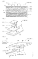
Fig. 1 illustrates a cross-sectional structure of a sensor unit of a fluorescent sensor in the related art. -
Fig. 2 is an exploded view for explaining the structure of the sensor unit of the fluorescent sensor in the related art. -
Fig. 3 illustrates a sensor system having a fluorescent sensor of a first embodiment. -
Fig. 4 is an exploded view for explaining the structure of the fluorescent sensor of the first embodiment. -
Fig. 5 is a schematic view showing a cross-sectional structure of a sensor unit of the fluorescent sensor of the first embodiment. -
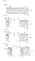
Fig. 6A is a schematic view showing a cross-sectional structure of the sensor unit in order to explain a method for manufacturing the fluorescent sensor of the first embodiment. -
Fig. 6B is a schematic view showing a cross-sectional structure of the sensor unit in order to explain the method for manufacturing the fluorescent sensor of the first embodiment. -
Fig. 6C is a schematic view showing a cross-sectional structure of the sensor unit in order to explain the method for manufacturing the fluorescent sensor of the first embodiment. -
Fig. 6D is a schematic view showing a cross-sectional structure of the sensor unit in order to explain the method for manufacturing the fluorescent sensor of the first embodiment. -
Fig. 6E is a schematic view showing a cross-sectional structure of the sensor unit in order to explain the method for manufacturing the fluorescent sensor of the first embodiment. -
Fig. 6F is a schematic view showing a cross-sectional structure of the sensor unit in order to explain the method for manufacturing the fluorescent sensor of the first embodiment. -
Fig. 6G is a schematic view showing a cross-sectional structure of the sensor unit in order to explain the method for manufacturing the fluorescent sensor of the first embodiment. -
Fig. 7 is a schematic view showing a cross-sectional structure of a sensor unit of a fluorescent sensor of a variation of the first embodiment. -
Fig. 8 is a schematic view showing a cross-sectional structure of a sensor unit of a fluorescent sensor of a second embodiment. - First, a
fluorescent sensor 30 and asensor system 1 according to the first embodiment of the present invention will be described. As shown inFig. 3 , thesensor system 1 includes thefluorescent sensor 30, amain body 40, and areceiver 45 which receives and records signals from themain body 40. The signals are transmitted or received between themain body 40 and thereceiver 45 in a wired or wireless manner. - The
fluorescent sensor 30 includes aneedle 34 which punctures a specimen, and aconnector 35 which is connected to a rear end of theneedle 34. Theneedle 34 includes anelongated needle body 33 and aneedle head 32 which includes a main functional unit, that is, asensor unit 10. Theneedle head 32, theneedle body 33, and theconnector 35 may be formed integrally by using the same material or may be formed separately and then connected together. - The
connector 35 is removably fitted into afitting section 41 of themain body 40. A plurality ofwires 51 to 54 extended from thesensor unit 10 of thefluorescent sensor 30 is electrically coupled with themain body 40 by mechanically fitting theconnector 35 to thefitting section 41 of themain body 40. - The
fluorescent sensor 30 is a needle-type sensor which can consecutively measure analyte density for a predetermined period, for example one week, after inserting thesensor unit 10 into a body. Alternatively, without inserting thesensor unit 10 into a body, extracted bodily fluid, or bodily fluid circulating in the body through a fluid channel outside the body, may be brought into contact with thesensor unit 10 outside the body. - The
main body 40 includes acontrol unit 42 which drives and controls thesensor unit 10, and aprocessing unit 43 which processes signals output from thesensor unit 10. Thecontrol unit 42 and theprocessing unit 43 each include a processing circuit such as a CPU, but both units may share the same CPU. Thecontrol unit 42 and/or theprocessing unit 43 may be arranged on theconnector 35 of thefluorescent sensor 30 or on thereceiver 45. - The
main body 40 further includes, for example, a radio antenna to transmit/receive radio signals to/from thereceiver 45 and a battery (not shown). In cases where themain body 40 transmits/receives the signals from thereceiver 45 with wire, themain body 40 includes a signal wire instead of a radio antenna. In cases where themain body 40 includes a memory unit having necessary capacity, thereceiver 45 may be omitted. - Next, the structure of the main functional unit, that is, the
sensor unit 10 of thefluorescent sensor 30 will be described with reference toFigs. 4 and5 . Each drawing is a schematic view for explanation, and is different from an actual unit in horizontal/vertical dimensional ratio and the like, and also there is a case where some components are not illustrated. A shown inFigs. 4 and5 is referred to as direction upward. - The
fluorescent sensor 30 includes, as main functional components, a detectingsubstrate 11, afilter layer 14, anindicator 17, alight blocking layer 18, and a light emitting diode (LED)chip 15 which is a luminous element chip. - In the detecting
substrate 11 including semiconductor such as silicon, a through-hole 21 is formed, which penetrates a first main surface 11SA and a second main surface 11SB. - In wall surfaces 22 of the through-
hole 21, a photo diode (PD)element 12 is formed, which is a photoelectric conversion element that converts fluorescence into electric signals. That is, thePD element 12 is placed so as to encircle theindicator 17 arranged inside the through-hole 21 so that a light-receiving surface faces theindicator 17. ThePD element 12 may be formed in all or part of fourwall surfaces 22 of the rectangular through-hole 21. - On the other hand, on the second main surface 11SB of the detecting
substrate 11,detection signal wires PD element 12. Thedetection signal wire 51 is coupled with a light-receiving unit of thePD element 12 through a low-resistance region 12S which is of the same semiconductor-impurity type as the light-receiving unit of thePD element 12. Thedetection signal wire 52 is coupled with a low-resistance region 12H which is of the same semiconductor-impurity type as the detectingsubstrate 11. - On the second main surface 11SB of the detecting
substrate 11,drive signal wires signal electrodes LED chip 15. - A transparent
protective layer 16 and afilter layer 14 are arranged so as to cover thePD element 12 formed in the wall surfaces 22. That is, theprotective layer 16 and thefilter layer 14 are arranged on the light-receiving surface side of thePD element 12 so as to cover thePD element 12. Thefilter layer 14 blocks excitation light having a wavelength, for example, of 375 nm and transmits fluorescence having a wavelength, for example, of 460 nm. - In the
fluorescent sensor 30, theLED chip 15 is coupled with the detectingsubstrate 11 through atransparent connection layer 13. The dimension of theLED chip 15 in a plan view is larger than the dimension of the opening of the second main surface 11SB of the through-hole 21. Accordingly, theLED chip 15 thoroughly covers a region just below the opening of the second main surface 11SB of the through-hole 21. In other words, a bottom surface of the through-hole 21 includes theconnection layer 13 which is on the top of theLED chip 15. - The
connection layer 13 is a protective layer which covers the surface of theLED chip 15 and the second main surface 11SB of the detectingsubstrate 11. Usable materials for theconnection layer 13 include organic resins such as an epoxy resin, a silicone resin, and a transparent amorphous fluorinated resin, and transparent inorganic materials such as a silicon oxide film and a silicon nitride film. Theconnection layer 13 is selected from materials having electric insulation properties, fluid barrier properties, and excellent transmission of excitation light. - The
connection layer 13 may have an opening in a region just below the opening of the second main surface 11SB of the through-hole 21. In this case, the bottom surface of the through-hole 21 will be the surface of theLED chip 15. Preferred materials for theconnection layer 13 include one which blocks excitation light. - The
indicator 17 arranged inside the through-hole 21 generates fluorescence of intensity corresponding to the density of theanalyte 2, by means of interaction with the enteredanalyte 2 and the excitation light. The thickness of theindicator 17 is about several tens of µm to several hundred µm. Theindicator 17 is provided with a base material including a fluorescent dye which generates fluorescence of intensity corresponding to an amount of theanalyte 2 having entered the indicator, that is, analyte density in a solution to be measured. - The
light blocking layer 18 covering the opening of the first main surface 11SA of the through-hole 21 has a thickness of about several tens of µm. Thelight blocking layer 18 prevents excitation light and fluorescence from leaking outside and also prevents outside light from entering inside. Further, thelight blocking layer 18 has analyte permeability and does not prevent theanalyte 2 from passing therethrough. - An anti-light-leaking
layer 19 arranged so as to cover the bottom surface (undersurface) and the side surface of theLED chip 15 prevents, from leaking outside, the excitation light emitted from the bottom and side surfaces and the excitation light reflected from the second main surface 11SB of the detectingsubstrate 11. That is, although the anti-light-leakinglayer 19 has a similar function to thelight blocking layer 18, analyte permeability is not necessary for the anti-light-leakinglayer 19. - Next, a method for manufacturing the
fluorescent sensor 30 will be briefly described with reference toFigs. 6A to 6G. Figs. 6A to 6G are partial sectional views showing a region of onesensor unit 10 of thefluorescent sensor 30, but in the actual process, a plurality of thesensor units 10 of thefluorescent sensor 30 is collectively manufactured as a wafer process. - First, as shown in
Fig. 6A , the low-resistance regions PD element 12 are formed on the second main surface 11SB of a silicon wafer (detecting substrate) 11W by implanting impurities, using an ordinary semiconductor process. - That is, the low-
resistance region 12S is formed by introducing impurities of the same semiconductor-impurity type as the light-receiving unit of thePD element 12, while the low-resistance region 12H is formed by introducing impurities of the same semiconductor-impurity type as asilicon wafer 11. For example, in cases where the light-receiving unit of the PD element is a P-type semiconductor, boron is introduced to the low-resistance region 12S, while phosphorous or arsenic is introduced to the low-resistance region 12H. - For materials of the detecting
substrate 11, a single-crystal silicon is preferable in order to form thePD element 12 in the surface thereof, but glass or ceramic may be employed as well. In cases where the detectingsubstrate 11 includes glass and the like, a photoelectric conversion element is formed as the wall surfaces 22 of the through-hole 21 are coated with a semiconductor layer such as polysilicon. - As a photoelectric conversion element, a photoconductor element or a photo transistor element may be employed as well.
- Next, as shown in
Fig. 6B , through amask layer 71 having an opening in a through-hole forming section, thesilicon wafer 11W is etched from the side of the second main surface 11SB to form the through-hole 21. Various known methods can be employed for etching. The low-resistance region 12S is removed by etching except for a region connected with thedetection signal wire 51. - A sectional configuration and measurement of the through-
hole 21 is designed according to the specification of thefluorescent sensor 30. The sectional measurement of the through-hole 21 is preferably shaped in an elongated configuration, such as 150 µm in lengthwise direction and 500 µm in crosswise direction, since thesensor unit 10 is arranged at the position of theneedle head 32. On the other hand, the sectional configuration (configuration in a plan view) of the through-hole 21 may be polygon, circle, ellipse or the like, but is preferably rectangle as it has high opening efficiency and is easy to process. - Next, as shown in
Fig. 6C , thePD element 12 as the light-receiving unit is formed in the wall surfaces 22 of the through-hole 21. That is, themask layer 71, in which a formation region of the through-hole 21 is an opening thereof, is arranged on thesilicon wafer 11W. Thesilicon wafer 11W is inclined at 5 to 30 degrees, and ion implantation is carried out at least from four directions. For example, in cases where thesilicon wafer 11W is of N-type, boron (B) is implanted at accelerating voltage of 10 to 200 keV, and in implantation amount of 1 × 10¹⁵ to 1 × 1016 cm-2. In this case, a thin oxide layer having a thickness of 10 to 100 nm may be placed on the wall surfaces 22 of the through-hole 21. By heat treatment after ion implantation, thePD element 12 connected to the low-resistance region 12S is formed in the wall surfaces 22. Themask layer 71 is removed after heat treatment. - As shown in
Fig. 6D , theprotective layer 16 and thefilter layer 14 are arranged in sequence by performing the CVD method or the like so as to cover thePD element 12 of the wall surfaces 22 of the through-hole 21 in thesilicon wafer 11W. - The
protective layer 16 is a single-layer film of an inorganic insulation layer such as a silicon oxide layer and a silicon nitride layer, or a multi-layer layer obtained by laminating the single-layer films. For theprotective layer 16, a layer having high transmission of fluorescence can be used, such as a silicon oxide layer, a silicon nitride layer, a multi-laminated layer including silicon oxide and silicon nitride layers, a silicone resin layer, or a transparent amorphous fluorinated resin layer. - The
filter layer 14 may be of multiple-interference type, but is preferably of absorption type such as a single-layer including silicon, a silicon carbide, an oxide silicon, a nitride silicon or organic materials, and a multi-layer obtained by laminating the single-layer. For example, a silicon layer and a silicon carbide layer have transmission of 10-5% or less at a wavelength of 375 nm, while having transmission of 10% or less at a wavelength of 460 nm. That is, the proportion of (transmission at excitation light wavelength/transmission at fluorescence wavelength) has selective permeability with a six-digit difference or more. Thefilter layer 14 may be a band pass filter which only transmits the fluorescence generated from theindicator 17. - The
filter layer 14 is preferably arranged not only on the wall surfaces 22 but also on the second main surface 11SB. Thefilter layer 14 arranged on the second main surface 11SB has an effect to lower noise level of thePD element 12 in order to prevent excitation light from entering the detectingsubstrate 11. - That is, the
fluorescent sensor 30 in which thefilter layer 14 is arranged on the second main surface 11SB has high sensitivity, since an S/N ratio of the detection signal output by thePD element 12 is high. - Next, as shown in
Fig. 6E , thedetection signal wires drive signal wires detection signal wires PD element 12, while thedrive signal wires LED chip 15 with drive signals. - Examples of materials used for the
detection signal wires signal wires interlayer insulation layer 59 include inorganic insulation materials such as a silicon oxide film or a silicon nitride film, and organic insulation materials such as polyimide. - In order to prevent the excitation light generated from the
LED chip 15 from entering the detectingsubstrate 11, thedetection signal wires drive signal wires - As shown in
Fig. 6E , thefluorescent sensor 30 has a multi-layer wire structure in which thedetection signal wires drive signal wires interlayer insulation layer 59. However, thedetection signal wires drive signal wires - In the case of the multi-layer wire structure, the
interlayer insulation layer 59 is formed between thedetection signal wires drive signal wires interlayer insulation layer 59 is also formed on the surface of thefilter layer 14 on the wall surfaces of the through-hole 21, theinterlayer insulation layer 59 preferably includes transparent materials such as oxide silicon similar to theprotective layer 16. Theinterlayer insulation layer 59 formed on the surface of thefilter layer 14 has a function to protect thefilter layer 14. - Next, as shown in
Fig. 6F , theLED chip 15 is coupled through theconnection layer 13 so as to cover the opening of the second main surface 11SB of the through-hole 21 of the detectingsubstrate 11. - A luminous element chip is not restricted to the
LED chip 15 and is selected from chips on which a luminous element is formed, such as an organic EL element, an inorganic EL element, and a laser diode element. TheLED chip 15 is preferable from the viewpoint that theLED chip 15 has fluorescence transmission, light generation efficiency, wide wavelength selectivity of excitation light and generates little light with a wavelength other than ultraviolet which is to be excitation light. - The
connection layer 13 is manufactured by applying, for example, a resin and hardening the resin. By the CVD method or the like, a transparent SiO2 layer or a nitride silicon layer may be arranged on the surface to be coated with a resin. In order to electrically couple thedrive signal electrodes LED chip 15 with thedrive signal wires - That is, when the
LED chip 15 is connected to the second main surface 11SB of the detectingsubstrate 11, thedrive signal electrodes LED chip 15 are simultaneously electrically coupled with thedrive signal wires LED chip 15 and the detecting substrate are physically connected and also electrically coupled with each other, thefluorescent sensor 30 is easy to manufacture. Theconnection layer 13 also has a function as a sealing member which seals the electrically coupled parts. - The anti-light-leaking
layer 19 is arranged on the undersurface and the side surfaces of theLED chip 15. The material for the anti-light-leakinglayer 19 may be the same as that for thelight blocking layer 18, or may be organic resins containing carbon black, metals, a multi-layer film or a compound film containing those materials. TheLED chip 15 on which the anti-light-leakinglayer 19 is arranged beforehand may be connected to the detectingsubstrate 11. - As for the anti-light-leaking
layer 19, when a metallic film having a high reflection ratio such as a film made of aluminum or silver is used, the anti-light-leakinglayer 19 can obtain a function as a reflection film for reflecting excitation light radiated from the bottom and side surfaces of theLED chip 15 in the direction upward or in the direction toward theindicator 17. - The anti-light-leaking
layer 19 may be arranged on the entire undersurface, the side surface, and the upper surface which is not covered with thelight blocking layer 18, of the detectingsubstrate 11. Further, a first light blocking layer covering theLED chip 15 and a second light blocking layer covering the detectingsubstrate 11 together with the first light blocking layer may be arranged as well (seeFig. 7 ). - Next, as shown in
Fig. 6G , thesilicon wafer 11W is inverted upside down and theindicator 17 is arranged inside thereof from the opening of the first main surface 11SA of the through-hole 21. - A fluorescent dye is selected according to the type of the
analyte 2. If the fluorescent dye reversibly converts the intensity of fluorescence generated according to the amount of theanalyte 2, the fluorescent dye can be used in any case. In order to measure sugars such as glucose, thefluorescent sensor 30 uses, as the fluorescent dye, a ruthenium organic complex, a fluorescent phenylboronic acid derivative, or a material to be reversibly bound with glucose such as fluorescein bound with protein. - The
indicator 17 includes, for example, as a base material, a hydrogel which easily becomes hydroscopic, and contains the fluorescent dye inside the hydrogel or contains the fluorescent dye bound with the hydrogel. Examples of components of the hydrogel that can be used include polysaccharides such as methylcellulose and dextran, acrylate hydrogel produced by polymerizing monomers such as (meth)acrylamide, methyl acrylamide and hydroxyethyl acrylate, or urethane hydrogel produced from polyethylene glycol and diisocyanate. - The
indicator 17 may be connected, through an adhesive layer including a silane coupling agent or the like, to the wall surfaces 22 of the through-hole 21, to thelight blocking layer 18 on the upper surface, or to theconnection layer 13 on the undersurface. In cases where a region of theconnection layer 13 just below the through-hole 21 has an opening, theindicator 17 may be connected to the surface of theLED chip 15 which includes the bottom surface of the through-hole 21. - The
indicator 17 may be produced by filling the through-hole 21 with an indicator including a gel skeleton formation material before polymerizing, and then polymerizing after covering the opening with thelight blocking layer 18. For example, a phosphate buffer solution including a fluorescent dye, a gel skeleton formation material, and a polymerization initiator are inserted into the through-hole 21 and after leaving the resultant under nitrogen atmosphere for one hour, theindicator 17 is produced. As for the fluorescent dye, 9,10-bis[N-[2-(5,5-dimethylborinane-2-yl)benzyl]-N-[6'-[(acryloyl polyethylene glycol-3400)carbonylamino]-n-hexylamino]methyl]-2-acetylanthracene(F-PEG-AAm) is used. As for the gel skeleton formation material, acrylamide is used. As for the polymerization initiator, sodium peroxydisulfate and N,N,N',N'-tetramethylethylenediamine is used. - Finally, the
light blocking layer 18 is arranged so as to cover the opening of the first main surface 11SA of the through-hole 21. Examples of materials used for thelight blocking layer 18 include a metallic or ceramic inorganic lamella which has a porous structure in submicron size, a composite structure including hydrogels mixed with carbon black in the base material of an organic polymer such as polyimide and polyurethane, a resin obtained by mixing carbon black into an analyte permeable polymer such as celluloses and polyacrylamide, and a resin obtained by laminating the above. - As the
wafer 11W is individually divided, a plurality of thesensor units 10 is integrally manufactured. As eachsensor unit 10 is connected to the head of theneedle body 33 separately produced and extended from theconnector 35, thefluorescent sensor 30 is completed. - A method for manufacturing the fluorescent sensor is not restricted thereto, and may include, for example, individually dividing the
silicon wafer 11W shown inFig. 6E and connecting theLED chip 15 and the like to each detectingsubstrate 11. - Moreover, the
silicon wafer 11W may be processed and connected to theconnector 35 such that an extending portion of the detectingsubstrate 11 includes theneedle body 33 of theneedle 34. - As described above, the wafer process enables collective mass production of the
fluorescent sensors 30. Accordingly, thefluorescent sensor 30 with stable quality can be provided at a low price. - Next, a motion of the
fluorescent sensor 30 will be described. - The
LED chip 15 pulse emits excitation light having a center wavelength of 375 nm, for example, once every 30 seconds. For example, a pulse current flowing into theLED chip 15 is from 1 mA to 100 mA, and a pulse width of emitted light is from 1 ms to 100 ms. - The excitation light generated from the
LED chip 15 passes through theconnection layer 13 and enters theindicator 17. Theindicator 17 generates fluorescence of intensity corresponding to the density of theanalyte 2. Theanalyte 2 passes through thelight blocking layer 18 and enters theindicator 17. The fluorescent dye of theindicator 17 generates fluorescence having a wavelength of 460 nm, for example, which is longer than excitation light having a wavelength of 375 nm. - A part of the fluorescence generated from the
indicator 17 passes through thefilter layer 14 and theprotective layer 16, and then enters thePD element 12. In thePD element 12, the fluorescence is photoelectrically converted, photogenically charged, and then output as detection signals. - In the
fluorescent sensor 30, theprocessing unit 43 of themain body 40 carries out processing based on detection signals, that is, a current resulted from photogenic charges from thePD element 12 or a voltage resulted from accumulated photogenic charges, and estimates the amount of analyte. - The
fluorescent sensor 30 detects fluorescence by thePD element 12 formed in the wall surfaces 22 encircling theindicator 17. In other words, among the fluorescence emitted from theindicator 17 in two vertical directions and in four directions of side surfaces, i.e., in six directions in total, thefluorescent sensor 30 detects the fluorescence emitted in the four directions. Accordingly, although thefluorescent sensor 30 is small, it has high detection sensitivity. Similarly, thesensor system 1 including thefluorescent sensor 30 has high detection sensitivity. - That is, the
fluorescent sensor 30 has theLED chip 15 adjacent to theindicator 17 and detects the fluorescence generated from theindicator 17 with thePD element 12 formed in theadjacent surface 22. Accordingly, thefluorescent sensor 30, in spite of its ultra-small size, has high detection sensitivity. Further, as a plurality of fluorescent sensors can be collectively manufactured by processing one detecting substrate, thefluorescent sensor 30 is easy to process and is economical. - In the
fluorescent sensor 30 of the first embodiment, the wall surfaces 22 of the through-hole 21 are substantially vertical to the first main surface 11SA (second main surface 11SB). To the contrary, as shown inFig. 7 , in afluorescent sensor 30A of asensor system 1A according to a variation of the first embodiment, wall surfaces 22A of a through-hole 21A of adetection substrate 11A in asensor unit 10A have a taper configuration, that is, the wall surface thereof is inclined at a predetermined angle θ relative to the main surface, and an opening of a first main surface 11SA is larger than an opening of a second main surface 11SB. The through-hole 21A whose wall surfaces 22A have a taper configuration can be formed by wet etching which employs tetramethylammonium hydroxide (TMAH) solution, potassium hydroxide (KOH) solution and the like. - For example, in cases where a silicon (100) surface is used for the
silicon wafer 11W, anisotropic etching is performed in which the etching rate of a (111) surface becomes slow compared to the (100) surface, and the wall surfaces 22A of the through-hole 21A will be the (111) surface and the angle θ will be 54.7 degrees. - As the through-
hole 21A whose wall surfaces 22A are inclined has a larger area to form thePD element 12A than the through-hole 21 whose wall surfaces 22 are vertical, the through-hole 21A has not only higher sensitivity but also higher productivity as thePD element 12A is easily formed in the wall surfaces 22A. When the inclination angle θ of the wall surfaces 22A is from 30 to 70 degrees, the above effect will be noticeable. - As shown in
Fig. 7 , in thefluorescent sensor 30A, aconnection layer 13A includes a light blocking material having almost the same opening as the opening of the second main surface 11SB of the through-hole 21A. The first anti-light-leakinglayer 19 includes aluminum having high reflection ratio. Further, a second anti-light-leakinglayer 19A including a carbon-containing resin with high light blocking effect covers thelight blocking layer 18 of theneedle head 32 except for the upper side thereof. - Next, a
sensor system 1B and afluorescent sensor 30B of the second embodiment will be described. As thefluorescent sensor 30B and the like are similar to thefluorescent sensor 30 and the like, the same components are denoted with the same symbols and the explanation of the components is omitted. - As shown in
Fig. 8 , in a detectingsubstrate 11B of asensor unit 10B in thefluorescent sensor 30B, aPD element 12B is formed in addition to thePD element 12 which is the first photoelectric conversion element for detecting fluorescence generated from theindicator 17. ThePD element 12B is a second photoelectric conversion element for detecting excitation light generated from anLED chip 15L. That is, a light-receiving unit of thefirst PD element 12 is formed in the wall surfaces 22 of the through-hole 21 of the detectingsubstrate 11B, and a light-receiving unit of thesecond PD element 12B is formed in the second main surface 11SB. The first and second photoelectric conversion elements are PD elements having the same structure. - The
LED chip 15L covers not only a region just below an opening of the second main surface 11SB of the through-hole 21 but also a region just below thesecond PD element 12B. That is, the dimension of theLED chip 15L in a plan view is large enough to cover the region just below the opening of the through-hole 21 and the region just below thePD element 12B. - The
filter layer 14 is not arranged on the surface of thePD element 12B. Accordingly, thePD element 12B outputs electric signals (detection signals) corresponding to the intensity of excitation light generated from theLED chip 15L. - A method for manufacturing the
fluorescent sensor 30B is similar to the method for manufacturing thefluorescent sensor 30. In the process shown inFig. 6A , the low-resistance regions PD element 12B is formed. ThePD element 12 in the wall surfaces of the through-hole 21 is formed in the process shown inFig. 6C similarly to thefluorescent sensor 30. - On the second main surface 11SB of the detecting
substrate 11B, adetection signal wire 55 is also arranged, which transmits detection signals output from thePD element 12B. Thedetection signal wire 52 connected to the low-resistance region 12H is a common wire of thePD element 12 and thePD element 12B. - The intensity of the fluorescence generated from the
indicator 17 increases or decreases as influenced not only by analyte density but also by the intensity of emitted excitation light. However, in thesensor system 1B, theprocessing unit 43 for processing the electric signals (detection signals) output from thefluorescent sensor 30B corrects the electric signals (detection signals) from thefirst PD element 12 based on electric signals from thesecond PD element 12B. - The
fluorescent sensor 30B and thesensor system 1B have the same effect as thefluorescent sensor 30, thesensor system 1 and the like. Further, thefluorescent sensor 30B and thesensor system 1B can carry out highly accurate measurement even when the intensity of the excitation light has been changed by luminous efficiency dispersion of theLED chip 15L or by excitation light amount drift during operation. - The
fluorescent sensor 30B can obtain the same effect as thefluorescent sensor 30A, by making the wall surfaces of the through-hole into a taper configuration. - In the above description, the
fluorescent sensor 30 and the like for detecting sugars such as glucose have been exemplified, but thefluorescent sensor 30 can be applied to various uses such as an enzyme sensor, a pH sensor, an immune sensor, and a microorganism sensor, depending on a fluorescent dye to be selected. For example, in order to measure hydrogen-ion concentration or carbon dioxide in vivo, a hydroxypyrene trisulfonic acid derivative and the like are employed as a fluorescent dye. In order to measure sugars, a phenyl boronic acid derivative having a fluorescence residue is employed as a fluorescent dye. In order to measure potassium ion, a crown ether derivative having a fluorescence residue is employed as a fluorescent dye. - That is, the present invention is not restricted to the embodiments and the variation described above, but can be modified and/or revised in various ways as long as the gist of the present invention is not changed.
- This application is based upon and claims the benefit of priority from Japanese Patent Application No.
2012-031964
Claims (8)
- A fluorescent sensor, comprising:a detecting substrate in which a photoelectric conversion element configured to convert fluorescence into an electric signal is formed in a wall surface of a through-hole which penetrates first and second main surfaces;an indicator arranged inside the through-hole and configured to generate the fluorescence of intensity corresponding to analyte density when the indicator receives excitation light;a filter layer which covers the photoelectric conversion element and is configured to transmit the fluorescence and block the excitation light;a light blocking layer which covers an opening of the first main surface of the through-hole, and through which the analyte passes; anda luminous element chip which covers a region just below an opening of the second main surface of the through-hole and is configured to generate the excitation light.
- The fluorescent sensor according to claim 1, wherein the fluorescent sensor is a needle-type sensor having, on a needle head, a sensor unit including the detecting substrate, the filter layer, the indicator, the light blocking layer, and the luminous element chip.
- The fluorescent sensor according to claim 2, wherein a detection signal wire connected to the photoelectric conversion element and a drive signal wire connected to the luminous element chip are arranged on the second main surface.
- The fluorescent sensor according to claim 3, wherein the filter layer is also arranged on the second main surface.
- The fluorescent sensor according to claim 4, wherein the wall surface of the through-hole has a taper configuration.
- The fluorescent sensor according to claim 1, wherein a second photoelectric conversion element is formed in the second main surface, and
the luminous element chip covers the region just below the opening of the second main surface and a region just below the second photoelectric conversion element. - The fluorescent sensor according to claim 6, wherein the electric signal from the photoelectric conversion element is corrected by using an electric signal from the second photoelectric conversion element.
- A sensor system, comprising:a needle-type sensor having, on a needle head:a detecting substrate having a first photoelectric conversion element configured to convert fluorescence into an electric signal in a wall surface of a through-hole which penetrates first and second main surfaces and a second photoelectric conversion element in the second main surface;an indicator arranged inside the through-hole and configured to react to an analyte and generate the fluorescence of intensity corresponding to the density of the analyte when the indicator receives excitation light;a light blocking layer which covers an opening of the first main surface of the through-hole, and through which the analyte passes; anda luminous element chip which covers the region just below the opening of the second main surface and a region just below the second photoelectric conversion element, and is configured to generate the excitation light; anda processing unit configured to correct the electric signal from the photoelectric conversion element by using an electric signal from the second photoelectric conversion element.
Applications Claiming Priority (2)
| Application Number | Priority Date | Filing Date | Title |
|---|---|---|---|
| JP2012031964 | 2012-02-16 | ||
| PCT/JP2013/051419 WO2013121850A1 (en) | 2012-02-16 | 2013-01-24 | Fluorescent sensor and sensor system |
Publications (2)
| Publication Number | Publication Date |
|---|---|
| EP2818849A1 true EP2818849A1 (en) | 2014-12-31 |
| EP2818849A4 EP2818849A4 (en) | 2015-10-07 |
Family
ID=48983971
Family Applications (1)
| Application Number | Title | Priority Date | Filing Date |
|---|---|---|---|
| EP13748980.3A Withdrawn EP2818849A4 (en) | 2012-02-16 | 2013-01-24 | Fluorescent sensor and sensor system |
Country Status (5)
| Country | Link |
|---|---|
| US (1) | US20140349383A1 (en) |
| EP (1) | EP2818849A4 (en) |
| JP (1) | JP6087337B2 (en) |
| CN (1) | CN104126113B (en) |
| WO (1) | WO2013121850A1 (en) |
Families Citing this family (7)
| Publication number | Priority date | Publication date | Assignee | Title |
|---|---|---|---|---|
| CN108878461A (en) * | 2017-05-08 | 2018-11-23 | 中芯国际集成电路制造(上海)有限公司 | Semiconductor devices and its manufacturing method |
| CN108712826B (en) * | 2018-08-09 | 2023-12-01 | 深圳凯世光研股份有限公司 | A PCB board Mark point identification device and its identification method |
| CN109103744A (en) * | 2018-09-03 | 2018-12-28 | 业成科技(成都)有限公司 | Light emitting device and its manufacturing method |
| CN109738403A (en) * | 2019-01-03 | 2019-05-10 | 必欧瀚生物技术(合肥)有限公司 | A kind of preparation method of fluorescence standard card and fluorescence standard card fluorescent film |
| CN115399760A (en) * | 2021-05-26 | 2022-11-29 | 南京微纳科技研究院有限公司 | Implantable probe and implantable sensor |
| CN114166805B (en) * | 2021-11-03 | 2024-01-30 | 格力电器(合肥)有限公司 | NTC temperature sensor detection method and device, NTC temperature sensor and manufacturing method |
| PT119433A (en) * | 2024-04-26 | 2025-10-27 | Univ Nova De Lisboa | Multilayer optical sensor for detecting pesticides in oil and detector device comprising the same. |
Family Cites Families (11)
| Publication number | Priority date | Publication date | Assignee | Title |
|---|---|---|---|---|
| US5894351A (en) * | 1997-05-13 | 1999-04-13 | Colvin, Jr.; Arthur E. | Fluorescence sensing device |
| US6197503B1 (en) * | 1997-11-26 | 2001-03-06 | Ut-Battelle, Llc | Integrated circuit biochip microsystem containing lens |
| CA2445127C (en) * | 2001-05-04 | 2011-12-13 | Sensors For Medicine And Science, Inc. | Electro-optical sensing device with reference channel |
| US6844563B2 (en) * | 2001-05-22 | 2005-01-18 | Matsushita Electric Industrial Co., Ltd. | Fluorescence detecting device with integrated circuit and photodiode, and detection method |
| JP2002350347A (en) * | 2001-05-22 | 2002-12-04 | Matsushita Electric Ind Co Ltd | Fluorescence detector |
| US20040161853A1 (en) * | 2003-02-13 | 2004-08-19 | Zhongping Yang | Implantable chemical sensor with rugged optical coupler |
| JP5076142B2 (en) * | 2006-12-29 | 2012-11-21 | 国立大学法人徳島大学 | Fluorometer |
| WO2010119916A1 (en) * | 2009-04-13 | 2010-10-21 | Olympus Corporation | Fluorescence sensor, needle-type fluorescence sensor, and method for measuring analyte |
| JP2012031964A (en) | 2010-08-02 | 2012-02-16 | Ntn Corp | Reverse input cutoff clutch |
| JP5638343B2 (en) * | 2010-10-25 | 2014-12-10 | テルモ株式会社 | Fluorescent sensor |
| JP2012247260A (en) * | 2011-05-26 | 2012-12-13 | Olympus Corp | Fluorescence sensor |
-
2013
- 2013-01-24 EP EP13748980.3A patent/EP2818849A4/en not_active Withdrawn
- 2013-01-24 WO PCT/JP2013/051419 patent/WO2013121850A1/en not_active Ceased
- 2013-01-24 JP JP2014500142A patent/JP6087337B2/en active Active
- 2013-01-24 CN CN201380009728.4A patent/CN104126113B/en active Active
-
2014
- 2014-08-12 US US14/457,628 patent/US20140349383A1/en not_active Abandoned
Also Published As
| Publication number | Publication date |
|---|---|
| HK1199659A1 (en) | 2015-07-10 |
| EP2818849A4 (en) | 2015-10-07 |
| CN104126113B (en) | 2016-10-19 |
| CN104126113A (en) | 2014-10-29 |
| JP6087337B2 (en) | 2017-03-01 |
| US20140349383A1 (en) | 2014-11-27 |
| JPWO2013121850A1 (en) | 2015-05-11 |
| WO2013121850A1 (en) | 2013-08-22 |
Similar Documents
| Publication | Publication Date | Title |
|---|---|---|
| US20140349383A1 (en) | Fluorescent sensor and sensor system | |
| JP5307901B2 (en) | Fluorescence sensor, needle-type fluorescence sensor, and analyte measurement method | |
| US8853649B2 (en) | Fluorescence sensor | |
| US20040161853A1 (en) | Implantable chemical sensor with rugged optical coupler | |
| CN109659377A (en) | Single-photon avalanche diode and production method, detector array, imaging sensor | |
| US9885661B2 (en) | Analyte detection method, fluorescence detection method, and fluorescence detection apparatus using same | |
| CN102110704A (en) | Image sensor and method of manufacturing the same, and sensor device | |
| US20220120684A1 (en) | Waveguide integration with optical coupling structures on light detection device | |
| CN103824813B (en) | A kind of single chip integrated micro-system of fluorescence analysis and preparation method thereof | |
| JP2015059869A (en) | Fluorescence sensor | |
| HK1199659B (en) | Fluorescent sensor and sensor system | |
| WO2013161989A1 (en) | Fluorescence sensor | |
| WO2014045762A1 (en) | Fluorescent light sensor and sensor system | |
| WO2014045387A1 (en) | Fluorescent sensor | |
| JP2013076592A (en) | Needle type sensor and method for manufacturing needle type sensor | |
| WO2014045386A1 (en) | Fluorescent sensor | |
| WO2013161991A1 (en) | Fluorescence sensor | |
| WO2013094562A1 (en) | Fluorescence sensor, sensor system, and fluorescence sensor correction method | |
| JP2012247260A (en) | Fluorescence sensor | |
| WO2014045384A1 (en) | Fluorescent sensor | |
| WO2013161990A1 (en) | Fluorescent light sensor | |
| HK40060156A (en) | Waveguide integration with optical coupling structures on light detection device | |
| WO2014045385A1 (en) | Fluorescent sensor | |
| MXPA99010459A (en) | Improved fluorescence sensing device | |
| CN104807792A (en) | Negative refractive index photonic crystal bioluminescence detector |
Legal Events
| Date | Code | Title | Description |
|---|---|---|---|
| PUAI | Public reference made under article 153(3) epc to a published international application that has entered the european phase |
Free format text: ORIGINAL CODE: 0009012 |
|
| 17P | Request for examination filed |
Effective date: 20140909 |
|
| AK | Designated contracting states |
Kind code of ref document: A1 Designated state(s): AL AT BE BG CH CY CZ DE DK EE ES FI FR GB GR HR HU IE IS IT LI LT LU LV MC MK MT NL NO PL PT RO RS SE SI SK SM TR |
|
| AX | Request for extension of the european patent |
Extension state: BA ME |
|
| DAX | Request for extension of the european patent (deleted) | ||
| RA4 | Supplementary search report drawn up and despatched (corrected) |
Effective date: 20150909 |
|
| RIC1 | Information provided on ipc code assigned before grant |
Ipc: G01N 21/77 20060101ALI20150903BHEP Ipc: G01N 21/64 20060101AFI20150903BHEP |
|
| STAA | Information on the status of an ep patent application or granted ep patent |
Free format text: STATUS: THE APPLICATION HAS BEEN WITHDRAWN |
|
| 18W | Application withdrawn |
Effective date: 20170331 |