EP2818323A1 - Stamping-face plate holder - Google Patents
Stamping-face plate holder Download PDFInfo
- Publication number
- EP2818323A1 EP2818323A1 EP14173899.7A EP14173899A EP2818323A1 EP 2818323 A1 EP2818323 A1 EP 2818323A1 EP 14173899 A EP14173899 A EP 14173899A EP 2818323 A1 EP2818323 A1 EP 2818323A1
- Authority
- EP
- European Patent Office
- Prior art keywords
- stamping
- face plate
- plate holder
- holding member
- paper board
- Prior art date
- Legal status (The legal status is an assumption and is not a legal conclusion. Google has not performed a legal analysis and makes no representation as to the accuracy of the status listed.)
- Granted
Links
Images



Classifications
-
- B—PERFORMING OPERATIONS; TRANSPORTING
- B23—MACHINE TOOLS; METAL-WORKING NOT OTHERWISE PROVIDED FOR
- B23Q—DETAILS, COMPONENTS, OR ACCESSORIES FOR MACHINE TOOLS, e.g. ARRANGEMENTS FOR COPYING OR CONTROLLING; MACHINE TOOLS IN GENERAL CHARACTERISED BY THE CONSTRUCTION OF PARTICULAR DETAILS OR COMPONENTS; COMBINATIONS OR ASSOCIATIONS OF METAL-WORKING MACHINES, NOT DIRECTED TO A PARTICULAR RESULT
- B23Q3/00—Devices holding, supporting, or positioning work or tools, of a kind normally removable from the machine
- B23Q3/18—Devices holding, supporting, or positioning work or tools, of a kind normally removable from the machine for positioning only
-
- B—PERFORMING OPERATIONS; TRANSPORTING
- B41—PRINTING; LINING MACHINES; TYPEWRITERS; STAMPS
- B41D—APPARATUS FOR THE MECHANICAL REPRODUCTION OF PRINTING SURFACES FOR STEREOTYPE PRINTING; SHAPING ELASTIC OR DEFORMABLE MATERIAL TO FORM PRINTING SURFACES
- B41D7/00—Shaping elastic or deformable material, e.g. rubber, plastics material, to form printing surfaces
-
- B—PERFORMING OPERATIONS; TRANSPORTING
- B41—PRINTING; LINING MACHINES; TYPEWRITERS; STAMPS
- B41J—TYPEWRITERS; SELECTIVE PRINTING MECHANISMS, i.e. MECHANISMS PRINTING OTHERWISE THAN FROM A FORME; CORRECTION OF TYPOGRAPHICAL ERRORS
- B41J2/00—Typewriters or selective printing mechanisms characterised by the printing or marking process for which they are designed
- B41J2/315—Typewriters or selective printing mechanisms characterised by the printing or marking process for which they are designed characterised by selective application of heat to a heat sensitive printing or impression-transfer material
-
- B—PERFORMING OPERATIONS; TRANSPORTING
- B41—PRINTING; LINING MACHINES; TYPEWRITERS; STAMPS
- B41J—TYPEWRITERS; SELECTIVE PRINTING MECHANISMS, i.e. MECHANISMS PRINTING OTHERWISE THAN FROM A FORME; CORRECTION OF TYPOGRAPHICAL ERRORS
- B41J2/00—Typewriters or selective printing mechanisms characterised by the printing or marking process for which they are designed
- B41J2/315—Typewriters or selective printing mechanisms characterised by the printing or marking process for which they are designed characterised by selective application of heat to a heat sensitive printing or impression-transfer material
- B41J2/32—Typewriters or selective printing mechanisms characterised by the printing or marking process for which they are designed characterised by selective application of heat to a heat sensitive printing or impression-transfer material using thermal heads
-
- B—PERFORMING OPERATIONS; TRANSPORTING
- B41—PRINTING; LINING MACHINES; TYPEWRITERS; STAMPS
- B41K—STAMPS; STAMPING OR NUMBERING APPARATUS OR DEVICES
- B41K1/00—Portable hand-operated devices without means for supporting or locating the articles to be stamped, i.e. hand stamps; Inking devices or other accessories therefor
- B41K1/02—Portable hand-operated devices without means for supporting or locating the articles to be stamped, i.e. hand stamps; Inking devices or other accessories therefor with one or more flat stamping surfaces having fixed images
-
- B—PERFORMING OPERATIONS; TRANSPORTING
- B41—PRINTING; LINING MACHINES; TYPEWRITERS; STAMPS
- B41K—STAMPS; STAMPING OR NUMBERING APPARATUS OR DEVICES
- B41K1/00—Portable hand-operated devices without means for supporting or locating the articles to be stamped, i.e. hand stamps; Inking devices or other accessories therefor
- B41K1/36—Details
- B41K1/38—Inking devices; Stamping surfaces
- B41K1/50—Stamping surfaces impregnated with ink, or made of material leaving a mark after stamping contact
-
- B—PERFORMING OPERATIONS; TRANSPORTING
- B41—PRINTING; LINING MACHINES; TYPEWRITERS; STAMPS
- B41K—STAMPS; STAMPING OR NUMBERING APPARATUS OR DEVICES
- B41K3/00—Apparatus for stamping articles having integral means for supporting the articles to be stamped
- B41K3/62—Details or accessories
Definitions
- the present invention relates to a stamping-face plate holder not expensive in producing costs and simple in configuration, used for making a stamping-face plate of a stamp.
- Japanese Unexamined Patent Publication No. Hei 07-251558 proposes a method of producing a stamp.
- a thermal printer having a thermal head is used, and a cassette case which contains a roll of a tape of sponge material for making a stamp plate is installed on the thermal printer, and a printing image entered to the thermal printer is printed on the material pulled out from the cassette case with the thermal head to make a stamping-face plate of a stamp.
- the cassette case containing the sponge material for making a stamp plate is used, and when all the sponge material for making a stamp plate has been used up, the cassette case will be a waste product, inviting a trouble that such waste product will raise commodity expenses.
- the thermal printer using the cassette case containing the material for making a stamp plate will be complex in mechanism and large in scale for making stamps of various sizes of stamping-face plates.
- the maximum size of material for making a stamp plate is used to make stamps of various sizes of stamping-face plates, excess of the material will also increase and such excess material will raise commodity expenses.
- Japanese Unexamined Patent Publication No. Hei 10-100464 discloses a device for making a stamp whose stamping-face plate consisting of an ink permeable portion and an ink non-permeable portion.
- a thermal head of the device has plural needle-like heating elements and the heating elements are selectively pressed on a porous sheet and heated to make the ink permeable portion and ink non-permeable portion of the stamping-face plate.
- the device disclosed in Japanese Unexamined Patent Publication No. Hei 10-100464 has a large-scale driving mechanism using a carriage for carrying the thermal head, which is impossible to meet a recent market demand for downsizing.
- edge heads are expansive compared with normal thermal heads. They are about three times as expansive as the normal heads. Generally, the device using the edge head will receive limitation in freedom for design.
- the present invention has been made to solve the problems involved in the conventional techniques and provides a stamping-face plate holder not expensive in producing costs and simple in configuration, used for making a stamping-face plate of a stamp.
- a stamping-face plate holder which comprises a plate holding member that detachably holds a stamping-face plate, the stamping-face plate including a porous material impregnated with ink, and a film that covers at least a portion of the stamping-face plate held in the plate holding member.
- FIG. 1 is a block diagram of a system configuration of a thermal printer for making a plate, which uses a stamping-face plate holder according to the first embodiment of the present invention.
- the thermal printer 1 comprises a central controlling circuit 2, a thermal head 3, a power source circuit 4, a motor driver 5, a stepping motor 6, a displaying device 7, a displaying-image controlling circuit 8, a memory controlling circuit 9, a user/interface controlling circuit 10, a USB controlling circuit 11, and Bluetooth (Registered Trademark) module/wireless LAN module 12.
- a central controlling circuit 2 a thermal head 3
- a power source circuit 4 a motor driver 5, a stepping motor 6, a displaying device 7, a displaying-image controlling circuit 8, a memory controlling circuit 9, a user/interface controlling circuit 10, a USB controlling circuit 11, and Bluetooth (Registered Trademark) module/wireless LAN module 12.
- all the displaying device 7, the displaying-image controlling circuit 8, the user/interface controlling circuit 10, USB controlling circuit 11, and Bluetooth (Registered Trademark) module/wireless LAN module 12 are not essential elements of the thermal printer 1.
- the thermal printer has to be directly or wirelessly connected with a personal computer (PC) 13, since a user operates on GUI (Graphical User Interface) of the personal computer 13 or a cellular phone terminal (not shown), the displaying-image controlling circuit 8 and the displaying device 7 are not essential elements for the thermal printer 1.
- PC personal computer
- GUI Graphic User Interface
- the central controlling circuit 2 controls the operation of the whole system.
- all the elements are connected only to the central controlling circuit 2, but these elements are connected to each other through a bus (not shown) for effecting data communication.
- the memory controlling circuit 9 contains devices such as ROM (Read Only Memory) and RAM (Random Access Memory), and controls these devices.
- the displaying device 7 is a displaying device such as LCD (Liquid Crystal Display), and the displaying-image controlling circuit 8 serves to transfer data to the displaying device 7 and also to control turn-on/turn-of f of a back-light operation of the displaying device 7.
- the user/interface controlling circuit 10 serves to control displaying of a menu image in accordance with information entered through an input device such as a keyboard, a mouse, a remote control device, a button, and touch panel.
- the power source circuit 4 consists of a power source IC (Integrated Circuit) and the like, and serves to supply the circuits with a required power.
- the thermal head 3 receives data and a printing signal output from the central controlling circuit 2 to control a built-in driver IC, thereby performing energization of printing dots.
- a printing medium such as a material of porous ethylene-vinyl acetate copolymer (hereinafter, referred to as "EVA"), then printing is performed on same printing medium.
- EVA porous ethylene-vinyl acetate copolymer
- the thermal head 3 has a resolution of 200 dots/25.4 mm and an effective printing width of 48 mm.
- the motor driver 5 receives a driving signal from output the central controlling circuit 2 to supply the stepping motor 6 with driving power. In practice, the motor driver 5 receives only an exciting signal from the central controlling circuit 2 and obtains actual power from the power source circuit 4.
- the central controlling circuit 2 counts the number of pulse signals supplied to the motor driver 5, thereby precisely confirming how much it has made the stepping motor 6 rotate, that is, how much or how long it has transported the printing medium.
- an one-two phase excitation driving system is employed for transporting the printing medium, and a gear ratio consists of 16 steps/line (0.125 mm). In other words, the printing medium is transported by 0.0078 mm/step.
- FIG. 2 (a) is an external perspective view of the thermal printer 1 according the first embodiment of the invention.
- FIG. 2 (b) is a sectional side view of the thermal printer 1 according the first embodiment of the invention.
- the thermal printer 1 has a printing-medium insertion opening 14 and a printing-medium discharge opening 16.
- the thermal printer 1 is shown in FIG. 2(a) , with a stamping-face plate holder 15 inserted into the printing-medium insertion opening 14 and with the leading end 15a of the stamping-face plate holder 15 coming out from the printing-medium discharge opening 16.
- the stamping-face plate holder 15 holds a stamping-face plate 17.
- the thermal printer 1 is shown in FIG. 2(b) , with the leading end 15a of the stamping-face plate holder 15 inserted into the printing-medium insertion opening 14. As shown in FIG. 2(b) , the leading end 15a of the stamping-face plate holder 15 has been inserted as far as to the position of the thermal head 18. Along a transporting course of the stamping-face plate holder 15, there are provided a sensor 19 and a platen roller 21.
- FIG. 3(a) is a plane view of the stamping-face plate holder 15 holding the stamping-face plate 17.
- FIG. 3(b) is a cross-sectional view of the stamping-face plate holder 15 taken along the line A-A' of FIG. 3(a).
- FIG. 3(c) is a rear view of the stamping-face plate holder 15.
- the stamping-face plate holder 15 serving as a holder that firmly holds the stamping-face plate 17 fixed at its central position.
- an arrow "a" indicates a direction in which the stamping-face plate holder 15 is inserted into the thermal printer 1.
- the stamping-face plate holder 15 consists of two thick paper boards (coated boards) 22 (top paper board 22a, bottom paper board 22b) integrated by adhering, as shown in FIG. 3 (b) .
- the stamping-face plate holder 15 has a cutout 25 for a sensor in its one lateral part (on the right side as seen in FIG. 3 (a) .
- the sensor 19 of the thermal printer 1 detects the cutout 25 of the stamping-face plate holder 15 to confirm a position for starting a printing operation and performing other controlling operations.
- a thermal printing operation for printing solid black data around on the leading end of the printing medium is performed based on the confirmation of the position for starting the printing operation.
- the thermal printing operation will be described in detail later. Since a controlling operation for confirming the position for starting the printing operation is not the substance of the present invention, and therefore further description thereof will not be made hereinafter.
- the top paper board 22a has a square recess 23 around at its central portion to receive the stamping-face plate 17 tightly therein.
- the stamping-face plate 17 is pressed into the recess 23 (hereinafter sometimes, referred to as the "positioning recess") to be held in position.
- the top paper board 22a has substantially the same thickness as the stamping-face plate 17 and is a little thinner than the stamping-face plate 17 within the range that no trouble is caused in the printing operation. This is because the printing operation is performed with the thermal head 18 pressed against onto the surface of the stamping-face plate 17 for enhancing the efficiency of heat conduction. It is also preferable that a difference in level between the top paper board 22a and the stamping-face plate 17 is not so large, to prevent the thermal head 18 from being caught by such difference during the printing operation.
- the stamping-face plate 17 is 1.5 mm in thickness and the top paper board 22a is 0.79 mm in thickness in the present embodiment.
- the bottom paper board 22b is made plain and also made to have the same external shape as the top paper board 22a.
- the bottom paper board 22b and the top paper board 22a are integrated together by adhering.
- the bottom paper board 22b supports the bottom surface of the stamping-face plate 17.
- the bottom paper board 22b is perforated (perforation 24) along the positioning recess 23 shown in FIG. 3(a) . At the top portion of the perforation 24 as seen in FIG.
- an arc-like cut in 24a is made and on the both sides of the cut in 24a, perforations 24b, 24b extending to the side edges of the bottom paper board 2 are made.
- the stamping-face plate 17 held in the stamping-face plate holder 15 is made of an ink-impregnated sponge body.
- the ethylene-vinyl acetate copolymer is used as a material of the sponge body.
- the surface of the top paper board 22a, and the top surface and sides of the stamping-face plate 17 exposing from the positioning recess 23 of the top paper board 22a are covered with a film 26.
- the film 26 is made of a base material such as PET (polyethylene terephthalate) and/or polyamide.
- the film 26 has a heat resistance, a heat conductivity and also a smoother surface.
- a material having a heat resistance to temperature higher than the melting point of the stamping-face plate 17 is used to make the film 26.
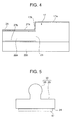
- FIG. 4 is an enlarged view showing the portion of the stamping-face plate holder 15 surrounded by the broken-line circle "a" in FIG. 3(b) . As shown in FIG. 4 , the top paper board 22a and the bottom paper board 22b are bonded together with a both-side adhesive sheet 27b.
- the film 26 covers the surface of the top paper board 22a excluding the portion corresponding to the positioning recess 23 where the stamping-face plate holder 15 is pressed into, and is bonded to said surface with a both-side adhesive sheet 27a.
- the film 26 covers the surface 17a and the side 17b of the stamping-face plate 17 exposing from the positioning recess 23 of the top paper board 22a but does not adhere to them. Therefore, when a plate making of the stamping-face plate 17 finishes as will be described later, the stamping-face plate 17 can be easily taken out from the stamping-face plate holder 15 by removing the bottom paper board 22b along the perforation 24 shown in FIG. 3(c) .
- the porous EVA is used to compose the stamping-face plate 17, and the surface of the porous EVA is heated with the thermal head to make the stamping-face plate of a stamp. Since the porous EVA (hereinafter, simply referred to as the "EVA") contains countless numbers of air bubbles, it is possible to impregnate EVA with liquid such as ink, just like sponges.
- EVA porous EVA
- EVA has a physical property of heat plasticity, and therefore, when EVA is heated, for instance, to 70 to 120 degrees centigrade, the heated portion softens and the portion which has softened once will harden when cooled down. The hardened portion loses air bubbles, turning to a non-porous portion and prevents liquid such as ink from passing through.
- this physical property (heat plasticity) of EVA is used.
- an arbitrary part of the surface of EVA (composing the stamping face of a stamp) is heated about 1 to 5 milliseconds by the thermal head, the arbitrary part of the surface of EVA (composing the stamping face of a stamp) turns to a non-porous part, preventing the ink impregnated therein from passing through.
- data of the seal impression drawn by the user represents a seal impression of 30 mm X 30 mm
- a seal impression to be subjected to the heating treatment by the thermal head has a size of 30 mm X 30 mm.
- stamping data which contains the seal impression edited by the user and further solid-black area surrounding said seal-impression is prepared in the present embodiment and used as data for making a plate of a seal impression.
- the solid-black area in the stamping data serves as an area for preventing the ink from seeping out.
- the data of the seal impression edited and produced by the user is subjected to the "black-white inverting process” and the “mirror-image inverting process” , and then the solid-black data is added to the processed seal-impression data, whereby the final stamping data to be supplied to the thermal printer is completed.
- EVA used for composing the stamping face of a stamp
- EVA is a material having 1.5 mm in thickness, and has a high elasticity coefficient and a high friction coefficient.
- the above difficulty in transporting EVA is a phenomenon that is caused even when the thermal head does not generate heat.
- the temperature of the thermal head rises to about 200 degrees centigrade within several milliseconds after it has started generating heat, and the surface of EVA has softened at the time when heated, and therefore the thermal head will sink in the softened EVA, preventing the stamping-face plate holder 15 with EVA (composing the stamping-face plate 17) held from moving anymore.
- the present invention has been made to provide the stamping-face plate holder 15, shown in FIGs. 2 (a) and 2(b) to FIG. 4 , which is used to make a stamping-face plate made of EVA.
- EVA is hard in transportation because of its flexibility and high friction coefficient.
- the thermal printer 1 provided with the normal thermal head, shown in FIG. 1 , FIG. 2(a) and FIG. 2(b) will be made small in size and cheap in manufacturing cost and uses the above stamping-face plate holder 15 to make a stamping-face plate made of EVA.
- stamping-face plate holder 15 in the first embodiment has been described with reference to FIGs. 3(a), 3(b), 3(c) and FIG. 4 in detail. Hereinafter, additional description of the stamping-face plate holder 15 will be given with respect to its functions and configuration.
- the stamping-face plate 17 is held in the positioning recess 23 of the top paper board 22a, supported from beneath by the bottom paper board 22b, and covered over with the film 26. Therefore, when held in the positioning recess 23 of the top paper board 22a, the stamping-face plate 17 is hard to be deformed even if it receives any external force.
- the stamping-face plate 17 can be transported as the user's intention and, also transported in the straight direction as user's intention.
- the film 26 has a heat-resisting property higher than the melting point of the stamping-face plate 17, that is, EVA.
- the film 26 covering over the plate 17 prevents the thermal head 18 from sinking into the plate 17, and allows the thermal head 18 to continue a heat-printing operation thereon smoothly, finishing making the stamping-face plate 17.
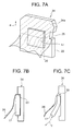
- FIG. 5 is a view showing a stamp consisting of a wood block with the stamping face attached, said stamping face being taken out from the stamping-face plate holder 15 after the making plate operation.
- the stamping-face plate 17 with the stamping face facing beneath is attached to the bottom of the wood block 30 with a both-side adhesive sheet 31.
- the wood block consists of a ball-like gripe 26 and a base block 29.
- the stamping-face portion of the stamp When the stamping-face portion of the stamp is dipped in ink for a given period of time, the ink impregnates into the stamping-face plate 17. After cleaning excessive ink on the stamping face, the user holds the ball-like gripe 26 to press the base block against the object. Then the ink seeps out from the stamping face to leave the seal impression on the object.
- the perforation 24 is made in the bottom paper board 22b along the positioning recess 23.
- the stamping-face plate 17 is taken out from the stamping-face plate holder 15, the user bends the bottom paper board 22b along the perforations 24b, 24b and grips the arc-like cut in 24a, striping off the portion surrounded by the perforation 24.
- both top paper board 22a and bottom paper board 22b in place of the perforation 24 of a four-sided figure.
- the user bends both the top and bottom paper boards 22a, 22b towards the top paper board side 22a.
- both the top and bottom paper boards 22a, 22b are cut and separated along the perforation 24b, but the film 26 still remains attached to the separated paper boards. Therefore, when the paper boards are further separated apart, the film 26 in the vicinity of the stamping-face plate 17 is peeled off from the top paper board 22a, allowing the user to take out the stamping-face plate 17 with the stamping face facing the user.
- the thick paper board (coated board) 22 from a single paper board instead of using two paper boards 22a, 22b and to provide at the center of the single paper board a concave portion for receiving and positioning the stamping-face plate 17.
- FIG. 6(a) is a plane view of the stamping-face plate holder 32 holding the stamping-face plate 17.
- FIG. 6(b) is a cross-sectional view of the stamping-face plate holder 32 taken along the line B-B' of FIG. 6(a).
- FIG. 6(c) is a rear view of the stamping-face plate holder 32.
- the stamping-face plate holder 32 serves as a holder and consists of a single paper board 22 which is provided with the positioning concave portion 33.
- the concave portion 33 holds and positions the stamping-face plate 17.
- stamping-face plate holder 32 In the stamping-face plate holder 32, only a single straight-line perforation 24b is made in place of the perforation of a four-sided figure ( FIG. 3(c) ) in the paper board 22, as shown in FIG. 6(a) and FIG. 6(c) .
- the end portion 32a of the stamping-face plate holder 32 is bent in the forward direction as indicated by an arrow "b" in FIG. 6(b) , the end portion 32a is cut and separated from the body of the stamping-face plate holder 32 along the perforation 24b.
- the film 26 in the vicinity of the stamping-face plate 17 is also peeled off from the paper board 22 together with the film 26 attached to the end portion 32a, allowing the user to take out the stamping-face plate 17 from the concave portion 33 of the stamping-face plate holder 32.
- FIGs. 7(a), 7(b) and 7(c) are views showing a configuration of a stamping-face plate holder in the third embodiment of the invention.
- the film 26 is bonded to the surface in the vicinity of the positioning recess 23 and/or the concave portion 33 with the both-side adhesive sheet 27b.
- the film 26 covers over the whole surface of the stamping-face plate holder 34, but the film 26 is bonded only to the surface of the front half portion 34a of the stamping-face plate holder 34 seen in the transport direction as indicated by an arrow "a" in FIG. 7 (a) with the both-side adhesive sheet 27b.
- the film 26 covers over the surface of the rear half portion of the stamping-face plate holder 34 but does not adhere to the portion.
- the user simply picks up at the end of the film 26 as shown in FIG. 7(b) , and can easily take out the stamping-face plate 17 from the stamping-face plate holder 34.
- stamping-face plate 17 can be replaced with another new plate, as indicated by an arrow "c" in FIG. 7(c) , the elements other than the stamping-face plate 17 can be used any number of times, and the stamping-face plate holder 34 can be made economical.
- the stamping-face plate holder consisting of a single paper board is shown in FIGs. 7(a), 7 (b) and 7(c) , but it is possible to use paper boards 22a, 22b to make the stamping-face plate holder and to provide the positioning recess 23 in place of the positioning concave portion 33.
- the positioning of the stamping-face plate 17 is not limited to those described herein, and any element which can fix the stamping-face plate 17 in place can be used in place of the positioning recess and the positioning concave portion.
- a hook-like gripper can be used as the positioning elements. It will be possible to use an adhesive material to detachably fix the two or four corners of the rear surface of the stamping-face plate 17 to the stamping-face plate holder 15.
- the size and configuration of the stamping-face plate holder 15 (32 and 34), and also the size and configuration of the stamping-face plate 17 are not restricted to those described in the embodiments of the invention, but may be arranged.
- the size of the stamping-face plate holder 15 (32 and 34) and the size of the stamping-face plate 17 in the direction perpendicular to the transporting direction (as indicated by the arrow "a" in FIG. 3 ) of the stamping-face plate holder 15 (32 and 34) is determined based on the configuration of the thermal printer 1, but the size of the stamping-face plate holder 15 (32 and 34) in its transporting direction (as indicated by the arrow "a” in FIG. 3 ) is not limited. Accordingly, there is no limitation in the size of the stamping-face plate 17 in the transporting direction (as indicated by the arrow "a” in FIG. 3 ) of the stamping-face plate holder 15 (32 and 34).
- the quality of material used for the stamping-face plate holder 15 is not limited to the coated board described in the embodiments, but any material can be used, which can hold the stamping-face plate 17 in place and transports the same steadily during the plate making.
- the stamping-face plate holder 15 is repeatedly used many times, and therefore, the material used to make the stamping- face plate holder 15 is selected placing priority on durability rather than on cheapness, different in other embodiments.
- the base material of the film 26 is not limited to PET (polyethylene terephthalate) and/or polyamide used in the embodiments, but any material which has a heat resistance to temperature higher than the melting point of the stamping-face plate 17 and has a heat conductivity required for the plate making and surface smoothness required for transporting the stamping-face plate holder 15 can be used as the base material of the film 26.
Landscapes
- Engineering & Computer Science (AREA)
- Mechanical Engineering (AREA)
- Manufacturing & Machinery (AREA)
- Manufacture Or Reproduction Of Printing Formes (AREA)
- Printing Plates And Materials Therefor (AREA)
Abstract
Description
- The present application is based upon and claims the benefit of priority from the prior Japanese Patent Application No.
2013-136947, filed June 28, 2013 - The present invention relates to a stamping-face plate holder not expensive in producing costs and simple in configuration, used for making a stamping-face plate of a stamp.
- In general, when affixing a seal on something, we used to use a stamp and put stamp ink on the stamping face of the stamp each time of affixing a seal. To avoid troublesome operation of putting the stamp ink on the stamp each time when affixing a seal, it is known to use a self-inking rubber stamp made of a material such as sponge rubber which is previously impregnated with stamp ink.
- For instance, Japanese Unexamined Patent Publication No.
Hei 07-251558 - In the technique proposed by Japanese Unexamined Patent Publication No.
Hei 07-251558 - The thermal printer using the cassette case containing the material for making a stamp plate will be complex in mechanism and large in scale for making stamps of various sizes of stamping-face plates. When the maximum size of material for making a stamp plate is used to make stamps of various sizes of stamping-face plates, excess of the material will also increase and such excess material will raise commodity expenses.
- Meanwhile, Japanese Unexamined Patent Publication No.
Hei 10-100464 - The device disclosed in Japanese Unexamined Patent Publication No.
Hei 10-100464 - Further, it is required to use an edge head as the thermal head, but the edge heads are expansive compared with normal thermal heads. They are about three times as expansive as the normal heads. Generally, the device using the edge head will receive limitation in freedom for design.
- The present invention has been made to solve the problems involved in the conventional techniques and provides a stamping-face plate holder not expensive in producing costs and simple in configuration, used for making a stamping-face plate of a stamp.
- According to one aspect of the invention, there is provided a stamping-face plate holder which comprises a plate holding member that detachably holds a stamping-face plate, the stamping-face plate including a porous material impregnated with ink, and a film that covers at least a portion of the stamping-face plate held in the plate holding member.
-
-
FIG. 1 is a block diagram of a system configuration of a thermal printer which uses a stamping-face plate holder to make a stamping-face plate, according to the first embodiment of the present invention. -
FIG. 2 (a) is an external perspective view of the thermal printer according the first embodiment of the invention. -
FIG. 2 (b) is a sectional side view of the thermal printer according the first embodiment of the invention. -
FIG. 3 (a) is a plane view of a stamping-face plate holder which holds the stamping-face plate. -
FIG. 3(b) is a cross-sectional view of the stamping-face plate holder taken along the line A-A' ofFIG. 3(a) . -
FIG. 3(c) is a rear view of the stamping-face plate holder. -
FIG. 4 is an enlarged view showing a portion surrounded by a broken-line circle "a" inFIG. 3(a) . -
FIG. 5 is a view showing a seal or stamp consisting of a wood block with the stamping-face plate attached, said stamping-face plate taken out from the finished stamping-face plate holder. -
FIG. 6(a) is a plane view of the stamping-face plate holder which holds the stamping-face plate (second embodiment) . -
FIG. 6 (b) is a cross-sectional view of the stamping-face plate holder taken along the line B-B' ofFIG. 6(a) (second embodiment). -
FIG. 6 (c) is a rear view of the stamping-face plate holder (second embodiment). -
FIGs. 7(a), 7(b) and 7(c) are views showing a stamping-face plate holder according to the third embodiment of the invention. - Now, the preferred embodiments of the present invention will be described with reference to the accompanying drawings in detail.
-
FIG. 1 is a block diagram of a system configuration of a thermal printer for making a plate, which uses a stamping-face plate holder according to the first embodiment of the present invention. - As shown in
FIG. 1 , thethermal printer 1 comprises a central controllingcircuit 2, athermal head 3, apower source circuit 4, amotor driver 5, astepping motor 6, a displayingdevice 7, a displaying-image controllingcircuit 8, amemory controlling circuit 9, a user/interface controlling circuit 10, aUSB controlling circuit 11, and Bluetooth (Registered Trademark) module/wireless LAN module 12. But, all the displayingdevice 7, the displaying-image controllingcircuit 8, the user/interface controlling circuit 10,USB controlling circuit 11, and Bluetooth (Registered Trademark) module/wireless LAN module 12 are not essential elements of thethermal printer 1. - For example, in the case where the thermal printer has to be directly or wirelessly connected with a personal computer (PC) 13, since a user operates on GUI (Graphical User Interface) of the
personal computer 13 or a cellular phone terminal (not shown), the displaying-image controllingcircuit 8 and the displayingdevice 7 are not essential elements for thethermal printer 1. - In the system configuration shown in
FIG. 1 , the central controllingcircuit 2 controls the operation of the whole system. InFIG. 2 , all the elements are connected only to the central controllingcircuit 2, but these elements are connected to each other through a bus (not shown) for effecting data communication. - The
memory controlling circuit 9 contains devices such as ROM (Read Only Memory) and RAM (Random Access Memory), and controls these devices. The displayingdevice 7 is a displaying device such as LCD (Liquid Crystal Display), and the displaying-image controllingcircuit 8 serves to transfer data to the displayingdevice 7 and also to control turn-on/turn-of f of a back-light operation of the displayingdevice 7. - The user/
interface controlling circuit 10 serves to control displaying of a menu image in accordance with information entered through an input device such as a keyboard, a mouse, a remote control device, a button, and touch panel. Thepower source circuit 4 consists of a power source IC (Integrated Circuit) and the like, and serves to supply the circuits with a required power. - The
thermal head 3 receives data and a printing signal output from the central controllingcircuit 2 to control a built-in driver IC, thereby performing energization of printing dots. When the printing dots of thethermal head 3 are energized and brought into contact with a printing medium such as a material of porous ethylene-vinyl acetate copolymer (hereinafter, referred to as "EVA"), then printing is performed on same printing medium. - In the system configuration of the present system, those that the peripheral circuits of the central controlling
circuit 2 receive from the central controllingcircuit 2 are only the data and the printing signal, and the peripheral circuits receive the power required for the printing operation from thepower source circuit 4. In addition, thethermal head 3 has a resolution of 200 dots/25.4 mm and an effective printing width of 48 mm. - The
motor driver 5 receives a driving signal from output the central controllingcircuit 2 to supply the steppingmotor 6 with driving power. In practice, themotor driver 5 receives only an exciting signal from the central controllingcircuit 2 and obtains actual power from thepower source circuit 4. - The central controlling
circuit 2 counts the number of pulse signals supplied to themotor driver 5, thereby precisely confirming how much it has made the steppingmotor 6 rotate, that is, how much or how long it has transported the printing medium. - In the
thermal printer 1 according to the present embodiment of the invention, an one-two phase excitation driving system is employed for transporting the printing medium, and a gear ratio consists of 16 steps/line (0.125 mm). In other words, the printing medium is transported by 0.0078 mm/step. -
FIG. 2 (a) is an external perspective view of thethermal printer 1 according the first embodiment of the invention.FIG. 2 (b) is a sectional side view of thethermal printer 1 according the first embodiment of the invention. As shown inFIG. 2(a) , thethermal printer 1 has a printing-medium insertion opening 14 and a printing-medium discharge opening 16. Thethermal printer 1 is shown inFIG. 2(a) , with a stamping-face plate holder 15 inserted into the printing-medium insertion opening 14 and with theleading end 15a of the stamping-face plate holder 15 coming out from the printing-medium discharge opening 16. The stamping-face plate holder 15 holds a stamping-face plate 17. - The
thermal printer 1 is shown inFIG. 2(b) , with theleading end 15a of the stamping-face plate holder 15 inserted into the printing-medium insertion opening 14. As shown inFIG. 2(b) , theleading end 15a of the stamping-face plate holder 15 has been inserted as far as to the position of thethermal head 18. Along a transporting course of the stamping-face plate holder 15, there are provided asensor 19 and aplaten roller 21. -
FIG. 3(a) is a plane view of the stamping-face plate holder 15 holding the stamping-face plate 17.FIG. 3(b) is a cross-sectional view of the stamping-face plate holder 15 taken along the line A-A' ofFIG. 3(a). FIG. 3(c) is a rear view of the stamping-face plate holder 15. As shown inFIG. 3(a) and FIG. 3(c) , the stamping-face plate holder 15 serving as a holder that firmly holds the stamping-face plate 17 fixed at its central position. InFIG. 3(a) , an arrow "a" indicates a direction in which the stamping-face plate holder 15 is inserted into thethermal printer 1. - The stamping-
face plate holder 15 consists of two thick paper boards (coated boards) 22 (top paper board 22a,bottom paper board 22b) integrated by adhering, as shown inFIG. 3 (b) . The stamping-face plate holder 15 has acutout 25 for a sensor in its one lateral part (on the right side as seen inFIG. 3 (a) . - When the stamping-
face plate holder 15 is inserted into thethermal printer 1, thesensor 19 of thethermal printer 1 detects thecutout 25 of the stamping-face plate holder 15 to confirm a position for starting a printing operation and performing other controlling operations. A thermal printing operation for printing solid black data around on the leading end of the printing medium is performed based on the confirmation of the position for starting the printing operation. The thermal printing operation will be described in detail later. Since a controlling operation for confirming the position for starting the printing operation is not the substance of the present invention, and therefore further description thereof will not be made hereinafter. - The
top paper board 22a has asquare recess 23 around at its central portion to receive the stamping-face plate 17 tightly therein. The stamping-face plate 17 is pressed into the recess 23 (hereinafter sometimes, referred to as the "positioning recess") to be held in position. - It is preferable that the
top paper board 22a has substantially the same thickness as the stamping-face plate 17 and is a little thinner than the stamping-face plate 17 within the range that no trouble is caused in the printing operation. This is because the printing operation is performed with thethermal head 18 pressed against onto the surface of the stamping-face plate 17 for enhancing the efficiency of heat conduction. It is also preferable that a difference in level between thetop paper board 22a and the stamping-face plate 17 is not so large, to prevent thethermal head 18 from being caught by such difference during the printing operation. - Just for information, the stamping-
face plate 17 is 1.5 mm in thickness and thetop paper board 22a is 0.79 mm in thickness in the present embodiment. - The
bottom paper board 22b is made plain and also made to have the same external shape as thetop paper board 22a. Thebottom paper board 22b and thetop paper board 22a are integrated together by adhering. When the stamping-face plate 17 is received in thepositioning recess 23 of thetop paper board 22a, thebottom paper board 22b supports the bottom surface of the stamping-face plate 17. As shown inFIG. 3(c) , thebottom paper board 22b is perforated (perforation 24) along thepositioning recess 23 shown inFIG. 3(a) . At the top portion of theperforation 24 as seen inFIG. 3(c) , an arc-like cut in 24a is made and on the both sides of the cut in 24a,perforations bottom paper board 2 are made. The stamping-face plate 17 held in the stamping-face plate holder 15 is made of an ink-impregnated sponge body. In the present embodiment, for example, the ethylene-vinyl acetate copolymer is used as a material of the sponge body. - As shown in
FIG. 3(b) , the surface of thetop paper board 22a, and the top surface and sides of the stamping-face plate 17 exposing from thepositioning recess 23 of thetop paper board 22a are covered with afilm 26. - The
film 26 is made of a base material such as PET (polyethylene terephthalate) and/or polyamide. Thefilm 26 has a heat resistance, a heat conductivity and also a smoother surface. A material having a heat resistance to temperature higher than the melting point of the stamping-face plate 17 is used to make thefilm 26. -
FIG. 4 is an enlarged view showing the portion of the stamping-face plate holder 15 surrounded by the broken-line circle "a" inFIG. 3(b) . As shown inFIG. 4 , thetop paper board 22a and thebottom paper board 22b are bonded together with a both-sideadhesive sheet 27b. - The
film 26 covers the surface of thetop paper board 22a excluding the portion corresponding to thepositioning recess 23 where the stamping-face plate holder 15 is pressed into, and is bonded to said surface with a both-sideadhesive sheet 27a. - Further, the
film 26 covers thesurface 17a and theside 17b of the stamping-face plate 17 exposing from thepositioning recess 23 of thetop paper board 22a but does not adhere to them. Therefore, when a plate making of the stamping-face plate 17 finishes as will be described later, the stamping-face plate 17 can be easily taken out from the stamping-face plate holder 15 by removing thebottom paper board 22b along theperforation 24 shown inFIG. 3(c) . - Now, the principle for making a stamping-face plate of a stamp in the present embodiment will be described briefly. As described above, the porous EVA is used to compose the stamping-
face plate 17, and the surface of the porous EVA is heated with the thermal head to make the stamping-face plate of a stamp. Since the porous EVA (hereinafter, simply referred to as the "EVA") contains countless numbers of air bubbles, it is possible to impregnate EVA with liquid such as ink, just like sponges. - Further, EVA has a physical property of heat plasticity, and therefore, when EVA is heated, for instance, to 70 to 120 degrees centigrade, the heated portion softens and the portion which has softened once will harden when cooled down. The hardened portion loses air bubbles, turning to a non-porous portion and prevents liquid such as ink from passing through.
- In the present embodiment, this physical property (heat plasticity) of EVA is used. When an arbitrary part of the surface of EVA (composing the stamping face of a stamp) is heated about 1 to 5 milliseconds by the thermal head, the arbitrary part of the surface of EVA (composing the stamping face of a stamp) turns to a non-porous part, preventing the ink impregnated therein from passing through.
- In other words, in a seal impression of a stamp, "the portions where the ink is allowed to pass through are not heated, and the portions where the ink is not allowed to pass through are heated by the thermal head. " In this way, the portions which allow the ink impregnated therein to seep out are formed in the seal impression.
- When this heating treatment by the thermal head is performed in place of the printing process executed in conventional thermal printers, white and black in stamping data representing the seal impression will be inverted.
- Using this phenomenon, when the white and black are turned over in accordance with the seal impression desired by a user and the surface of EVA is selectively heated, the ink impregnated in the heated portions is not allowed to pass through and the saturated ink is allowed to pass through in accordance with the seal impression formed with the not heated portions.
- From the portions not heated during the heating treatment performed on the surface of EVA, the ink impregnated therein can seep out. Therefore, the portions other than the portions of the seal impression that the user desires have to be heated to prevent the ink from seeping out there from.
- In general, it is inevitable in a mass production process that the central position of EVA (composing the stamping face of a stamp) is set a little out of the center line of the thermal head drawn on a design drawing, due to an assembly error. In practice, this discrepancy set in the production process between the central position of EVA and the center line of the thermal head can allow the ink to seep out from the portion that the user does not intend.
- More specifically, it is presumed that data of the seal impression drawn by the user represents a seal impression of 30
mm X 30 mm, and that a seal impression to be subjected to the heating treatment by the thermal head has a size of 30mm X 30 mm. - In the case where the position of EVA is set out of place by 1mm in a scanning direction, the center of the stamping face is not only set out of place by 1 mm but also the edge of EVA of 1 mm cannot be heated. As a result, the ink can seep out from there.
- To avoid the above trouble in the heating treatment by the thermal head, for example, stamping data which contains the seal impression edited by the user and further solid-black area surrounding said seal-impression is prepared in the present embodiment and used as data for making a plate of a seal impression. The solid-black area in the stamping data serves as an area for preventing the ink from seeping out.
- When a stamping face of 30
mm X 30 mm is provided to the users, the actual size of the stamping face will be (30 + a) mm X (30 + α) mm, where α = 1 mm to 2 mm. - What is to be edited and produced by the user is data of a seal impression to be stamped on an object. Therefore, in practice, the seal impression desired by the user is produced, and the mirror-image of the seal impression is inverted to produce data of the inverted mirror-image of the seal impression. Then, the data of the inverted mirror-image of the seal impression is used to make a plate of EVA (composing the stamping face of a stamp).
- In short, the data of the seal impression edited and produced by the user is subjected to the "black-white inverting process" and the "mirror-image inverting process" , and then the solid-black data is added to the processed seal-impression data, whereby the final stamping data to be supplied to the thermal printer is completed.
- By heating the surface of EVA (composing the stamping face of a stamp) based on the stamping data with the thermal head, it is possible to make a stamping-face plate having the seal impression unique to the user in a simple manner. The user bends the
bottom paper board 22b along theperforations FIG. 3 (c) ). Further, the user grips this arc-like cut in 24a to strip off the portion surrounded by theperforation 24, and can take out the completed stamping-face plate from the stamping-face plate holder 15. - EVA (used for composing the stamping face of a stamp) is a material having 1.5 mm in thickness, and has a high elasticity coefficient and a high friction coefficient. When the stamping-
face plate holder 15 with EVA (composing the stamping-face plate 17) held is inserted into thethermal printer 1 to be transported to position, the stamping-face plate holder 15 cannot be transported in a stable straight line because of great friction between the thermal head and EVA. - Even if the thermal printer is provided with guides for transporting the stamping-
face plate holder 15 smoothly and stably in a straight line, EVA can easily crook when the stamping-face plate holder 15 slightly turns the advancing direction because EVA is flexible and has an extremely large friction coefficient. - The above difficulty in transporting EVA is a phenomenon that is caused even when the thermal head does not generate heat. When the thermal head generates heat, the temperature of the thermal head rises to about 200 degrees centigrade within several milliseconds after it has started generating heat, and the surface of EVA has softened at the time when heated, and therefore the thermal head will sink in the softened EVA, preventing the stamping-
face plate holder 15 with EVA (composing the stamping-face plate 17) held from moving anymore. - As described above, in the system of using the edge head as the thermal head and in the system in which a carriage is installed in the head carrying mechanism, the above trouble will not be caused, but the above systems will invite another inconvenience that the mechanism will be large in size and costs of parts will increase.
- The present invention has been made to provide the stamping-
face plate holder 15, shown inFIGs. 2 (a) and2(b) to FIG. 4 , which is used to make a stamping-face plate made of EVA. As described above, EVA is hard in transportation because of its flexibility and high friction coefficient. More specifically, in the present embodiment of the present invention, thethermal printer 1 provided with the normal thermal head, shown inFIG. 1 ,FIG. 2(a) and FIG. 2(b) , will be made small in size and cheap in manufacturing cost and uses the above stamping-face plate holder 15 to make a stamping-face plate made of EVA. - The configuration of the stamping-
face plate holder 15 in the first embodiment has been described with reference toFIGs. 3(a), 3(b), 3(c) andFIG. 4 in detail. Hereinafter, additional description of the stamping-face plate holder 15 will be given with respect to its functions and configuration. - Four sides of the stamping-
face plate 17 held in thepositioning recess 23 of the stamping-face plate holder 15 are cut by a heat cutter. Therefore, the ink impregnated in the stamping-face plate 17 does not seep out from the four side surfaces. - The stamping-
face plate 17 is held in thepositioning recess 23 of thetop paper board 22a, supported from beneath by thebottom paper board 22b, and covered over with thefilm 26. Therefore, when held in thepositioning recess 23 of thetop paper board 22a, the stamping-face plate 17 is hard to be deformed even if it receives any external force. - Therefore, the stamping-
face plate 17 can be transported as the user's intention and, also transported in the straight direction as user's intention. Thefilm 26 has a heat-resisting property higher than the melting point of the stamping-face plate 17, that is, EVA. - Even though the surface of the stamping-
face plate 17 should be melted by thethermal head 18, thefilm 26 will not be melted. The friction between thethermal head 18 and thefilm 26 is extremely low. - Therefore, even though the surface of the stamping-
face plate 17 is melted and softened, thefilm 26 covering over theplate 17 prevents thethermal head 18 from sinking into theplate 17, and allows thethermal head 18 to continue a heat-printing operation thereon smoothly, finishing making the stamping-face plate 17. -
FIG. 5 is a view showing a stamp consisting of a wood block with the stamping face attached, said stamping face being taken out from the stamping-face plate holder 15 after the making plate operation. As shown inFIG. 5 , the stamping-face plate 17 with the stamping face facing beneath is attached to the bottom of thewood block 30 with a both-sideadhesive sheet 31. The wood block consists of a ball-like gripe 26 and abase block 29. - When the stamping-face portion of the stamp is dipped in ink for a given period of time, the ink impregnates into the stamping-
face plate 17. After cleaning excessive ink on the stamping face, the user holds the ball-like gripe 26 to press the base block against the object. Then the ink seeps out from the stamping face to leave the seal impression on the object. - In the first embodiment of the invention, the
perforation 24 is made in thebottom paper board 22b along thepositioning recess 23. When the stamping-face plate 17 is taken out from the stamping-face plate holder 15, the user bends thebottom paper board 22b along theperforations perforation 24. - In the second embodiment of the invention, only a straight-
line perforation 24b is made in bothtop paper board 22a andbottom paper board 22b in place of theperforation 24 of a four-sided figure. When taking out the stamping-face plate 17 from the stamping-face plate holder 15, the user bends both the top andbottom paper boards paper board side 22a. When bent, both the top andbottom paper boards perforation 24b, but thefilm 26 still remains attached to the separated paper boards. Therefore, when the paper boards are further separated apart, thefilm 26 in the vicinity of the stamping-face plate 17 is peeled off from thetop paper board 22a, allowing the user to take out the stamping-face plate 17 with the stamping face facing the user. - It is possible in the second embodiment of the invention to make the thick paper board (coated board) 22 from a single paper board instead of using two
paper boards face plate 17. -
FIG. 6(a) is a plane view of the stamping-face plate holder 32 holding the stamping-face plate 17.FIG. 6(b) is a cross-sectional view of the stamping-face plate holder 32 taken along the line B-B' ofFIG. 6(a). FIG. 6(c) is a rear view of the stamping-face plate holder 32. - As shown in
FIG. 6(b) , the stamping-face plate holder 32 serves as a holder and consists of asingle paper board 22 which is provided with the positioningconcave portion 33. As shown inFIG. 6 (a) and FIG. 6(b) , theconcave portion 33 holds and positions the stamping-face plate 17. - In the stamping-
face plate holder 32, only a single straight-line perforation 24b is made in place of the perforation of a four-sided figure (FIG. 3(c) ) in thepaper board 22, as shown inFIG. 6(a) and FIG. 6(c) . When theend portion 32a of the stamping-face plate holder 32 is bent in the forward direction as indicated by an arrow "b" inFIG. 6(b) , theend portion 32a is cut and separated from the body of the stamping-face plate holder 32 along theperforation 24b. When theend portion 32a is further separated away from the body, thefilm 26 in the vicinity of the stamping-face plate 17 is also peeled off from thepaper board 22 together with thefilm 26 attached to theend portion 32a, allowing the user to take out the stamping-face plate 17 from theconcave portion 33 of the stamping-face plate holder 32. -
FIGs. 7(a), 7(b) and 7(c) are views showing a configuration of a stamping-face plate holder in the third embodiment of the invention. In the stamping-face plate holders film 26 is bonded to the surface in the vicinity of thepositioning recess 23 and/or theconcave portion 33 with the both-sideadhesive sheet 27b. - But in the stamping-
face plate holder 34 in the third embodiment, thefilm 26 covers over the whole surface of the stamping-face plate holder 34, but thefilm 26 is bonded only to the surface of thefront half portion 34a of the stamping-face plate holder 34 seen in the transport direction as indicated by an arrow "a" inFIG. 7 (a) with the both-sideadhesive sheet 27b. Thefilm 26 covers over the surface of the rear half portion of the stamping-face plate holder 34 but does not adhere to the portion. - Therefore, when the plate making of the stamping-
face plate 17 has finished, the user simply picks up at the end of thefilm 26 as shown inFIG. 7(b) , and can easily take out the stamping-face plate 17 from the stamping-face plate holder 34. - Further, since the stamping-
face plate 17 can be replaced with another new plate, as indicated by an arrow "c" inFIG. 7(c) , the elements other than the stamping-face plate 17 can be used any number of times, and the stamping-face plate holder 34 can be made economical. The stamping-face plate holder consisting of a single paper board is shown inFIGs. 7(a), 7 (b) and 7(c) , but it is possible to usepaper boards positioning recess 23 in place of the positioningconcave portion 33. The positioning of the stamping-face plate 17 is not limited to those described herein, and any element which can fix the stamping-face plate 17 in place can be used in place of the positioning recess and the positioning concave portion. For example, a hook-like gripper can be used as the positioning elements. It will be possible to use an adhesive material to detachably fix the two or four corners of the rear surface of the stamping-face plate 17 to the stamping-face plate holder 15. - The size and configuration of the stamping-face plate holder 15 (32 and 34), and also the size and configuration of the stamping-
face plate 17 are not restricted to those described in the embodiments of the invention, but may be arranged. In particular, the size of the stamping-face plate holder 15 (32 and 34) and the size of the stamping-face plate 17 in the direction perpendicular to the transporting direction (as indicated by the arrow "a" inFIG. 3 ) of the stamping-face plate holder 15 (32 and 34) is determined based on the configuration of thethermal printer 1, but the size of the stamping-face plate holder 15 (32 and 34) in its transporting direction (as indicated by the arrow "a" inFIG. 3 ) is not limited. Accordingly, there is no limitation in the size of the stamping-face plate 17 in the transporting direction (as indicated by the arrow "a" inFIG. 3 ) of the stamping-face plate holder 15 (32 and 34). - The quality of material used for the stamping-
face plate holder 15 is not limited to the coated board described in the embodiments, but any material can be used, which can hold the stamping-face plate 17 in place and transports the same steadily during the plate making. - Particularly in the third embodiment of the invention, the stamping-
face plate holder 15 is repeatedly used many times, and therefore, the material used to make the stamping-face plate holder 15 is selected placing priority on durability rather than on cheapness, different in other embodiments. - The base material of the
film 26 is not limited to PET (polyethylene terephthalate) and/or polyamide used in the embodiments, but any material which has a heat resistance to temperature higher than the melting point of the stamping-face plate 17 and has a heat conductivity required for the plate making and surface smoothness required for transporting the stamping-face plate holder 15 can be used as the base material of thefilm 26. - Having described and illustrated the principles of the invention with reference to preferred embodiments of the invention, it should be apparent that the embodiments may be modified in arrangement and detail without departing from the principles disclosed herein and it is intended that the invention be concluded as including all such modifications and variations insofar as they come within the spirit and scope of such subject matter disclosed herein.
Claims (9)
- A stamping-face plate holder (15) comprising:a plate holding member (22) which detachably holds a stamping-face plate (17), the stamping-face plate (17) including a porous material impregnated with ink; anda film (26) which covers at least a portion of the stamping-face plate (17) held in the plate holding member (22) .
- The stamping-face plate holder (15) according to claim 1, wherein
the plate holding member (22) is formed with a positioning recess (23/33) for receiving and positioning the stamping-face plate (17). - The stamping-face plate holder (15) according to claim 2, wherein
the plate holding member (22) is formed with a perforation (24b) along at least one side of the positioning recess (23/33) and toward both sides of the plate holding member (22). - The stamping-face plate holder (15) according to claim 2, wherein
the plate holding member (22) is formed with a perforation (24) surrounding the positioning recess (23/33). - The stamping-face plate holder (15) according to any one of claims 1 to 4, wherein
the plate holding member (22) is made of a coated board. - The stamping-face plate holder (15) according to claim 5, wherein
the plate holding member (22) consists of at least a top paper board (22a) and a bottom paper board (22b), both boards having the same external shape and being integrated by adhering; and
the positioning recess (23) is formed in the top paper board (22a). - The stamping-face plate holder (15) according to any one of claims 1 to 6, wherein
the film (26) adheres to a surface of the plate holding member (22) surrounding the stamping-face plate (17) held in said plate holding member (22) and a portion of the film (26) covering the stamping-face plate (17) held in the plate holding member (22) does not adhere to said the stamping-face plate (17). - The stamping-face plate holder (15) according to any one of claims 1 to 6, wherein
a surface of the plate holding member (22) surrounding the stamping-face plate (17) held therein is divided into a first area and a second area; and
the film (26) covers and adheres to the first area and covers and does not adhere to the second area and the stamping- face plate (17) held in the plate holding member (22). - The stamping-face plate holder (15) according to any one of claims 1 to 8, wherein
the porous material of the stamping-face plate (17) is ethylene-vinyl acetate copolymer.
Applications Claiming Priority (1)
| Application Number | Priority Date | Filing Date | Title |
|---|---|---|---|
| JP2013136947A JP5812044B2 (en) | 2013-06-28 | 2013-06-28 | Stamp plate holder |
Publications (2)
| Publication Number | Publication Date |
|---|---|
| EP2818323A1 true EP2818323A1 (en) | 2014-12-31 |
| EP2818323B1 EP2818323B1 (en) | 2019-12-04 |
Family
ID=51176074
Family Applications (1)
| Application Number | Title | Priority Date | Filing Date |
|---|---|---|---|
| EP14173899.7A Active EP2818323B1 (en) | 2013-06-28 | 2014-06-25 | Stamping-face plate holder |
Country Status (4)
| Country | Link |
|---|---|
| US (1) | US9610665B2 (en) |
| EP (1) | EP2818323B1 (en) |
| JP (1) | JP5812044B2 (en) |
| CN (1) | CN104249575B (en) |
Families Citing this family (2)
| Publication number | Priority date | Publication date | Assignee | Title |
|---|---|---|---|---|
| JP5835294B2 (en) * | 2013-09-24 | 2015-12-24 | カシオ計算機株式会社 | Stamp holder |
| JP5958447B2 (en) * | 2013-11-06 | 2016-08-02 | カシオ計算機株式会社 | Stamp surface forming apparatus, stamp surface forming method, and stamp surface forming system |
Citations (6)
| Publication number | Priority date | Publication date | Assignee | Title |
|---|---|---|---|---|
| JPH07251558A (en) | 1993-12-28 | 1995-10-03 | Mitsubishi Pencil Co Ltd | Stamp manufacturing method |
| JPH10100464A (en) | 1996-10-01 | 1998-04-21 | Brother Ind Ltd | Printing plate manufacturing equipment |
| WO2002032668A1 (en) * | 2000-10-17 | 2002-04-25 | Humal Leo Henn | Method and apparatus for manufacturing of stamps from thermo-plastic micro porous material |
| JP2005161865A (en) * | 1995-08-10 | 2005-06-23 | Brother Ind Ltd | Stamp manufacturing method and apparatus |
| JP2009208294A (en) * | 2008-03-03 | 2009-09-17 | Shachihata Inc | Manufacturing equipment of porous stamp |
| JP2012153102A (en) * | 2011-01-28 | 2012-08-16 | Shachihata Inc | Method for manufacturing porous stamp |
Family Cites Families (12)
| Publication number | Priority date | Publication date | Assignee | Title |
|---|---|---|---|---|
| JP3212052B2 (en) * | 1993-10-28 | 2001-09-25 | ブラザー工業株式会社 | Plate making equipment |
| JPH10119403A (en) * | 1996-08-30 | 1998-05-12 | Seiko Epson Corp | Stamp material and stamp material set jig |
| US6276272B1 (en) * | 1996-10-01 | 2001-08-21 | Brother Kogyo Kabushiki Kaisha | Stamp plate producing apparatus for producing stamp plate used in a stamp device |
| JPH11138960A (en) * | 1997-11-12 | 1999-05-25 | Takasu Hirobumi | Stamp material for ink-permeable stamp and manufacture thereof |
| JP2000052631A (en) * | 1998-08-06 | 2000-02-22 | Riso Kagaku Corp | Stencil assembly for stencil printing |
| JP4168213B2 (en) | 1998-10-06 | 2008-10-22 | ブラザー工業株式会社 | Original sheet for creating stamps |
| JP2000211226A (en) * | 1999-01-20 | 2000-08-02 | Bando Chem Ind Ltd | Stamping material for stamp, stamp using the same, and manufacturing method thereof |
| JP4590725B2 (en) | 2000-12-07 | 2010-12-01 | ブラザー工業株式会社 | Plate making apparatus and attachment for plate making apparatus |
| JP2003154743A (en) * | 2001-11-19 | 2003-05-27 | Riso Kagaku Corp | Plate making method for simple stamp and simple stamp |
| US8777271B2 (en) * | 2008-12-18 | 2014-07-15 | Premier Print & Services Group, Inc. | Linerless packing and shipping label system |
| US9361811B2 (en) * | 2010-03-25 | 2016-06-07 | Emerald City Label, Inc. | Multi-layered label for a letter or package |
| JP6131538B2 (en) * | 2012-07-10 | 2017-05-24 | シヤチハタ株式会社 | Porous stamp material, method for producing the same, and stamp |
-
2013
- 2013-06-28 JP JP2013136947A patent/JP5812044B2/en active Active
-
2014
- 2014-06-25 US US14/314,946 patent/US9610665B2/en active Active
- 2014-06-25 CN CN201410290120.XA patent/CN104249575B/en active Active
- 2014-06-25 EP EP14173899.7A patent/EP2818323B1/en active Active
Patent Citations (6)
| Publication number | Priority date | Publication date | Assignee | Title |
|---|---|---|---|---|
| JPH07251558A (en) | 1993-12-28 | 1995-10-03 | Mitsubishi Pencil Co Ltd | Stamp manufacturing method |
| JP2005161865A (en) * | 1995-08-10 | 2005-06-23 | Brother Ind Ltd | Stamp manufacturing method and apparatus |
| JPH10100464A (en) | 1996-10-01 | 1998-04-21 | Brother Ind Ltd | Printing plate manufacturing equipment |
| WO2002032668A1 (en) * | 2000-10-17 | 2002-04-25 | Humal Leo Henn | Method and apparatus for manufacturing of stamps from thermo-plastic micro porous material |
| JP2009208294A (en) * | 2008-03-03 | 2009-09-17 | Shachihata Inc | Manufacturing equipment of porous stamp |
| JP2012153102A (en) * | 2011-01-28 | 2012-08-16 | Shachihata Inc | Method for manufacturing porous stamp |
Also Published As
| Publication number | Publication date |
|---|---|
| US20150001779A1 (en) | 2015-01-01 |
| EP2818323B1 (en) | 2019-12-04 |
| JP5812044B2 (en) | 2015-11-11 |
| CN104249575B (en) | 2017-04-12 |
| CN104249575A (en) | 2014-12-31 |
| US9610665B2 (en) | 2017-04-04 |
| JP2015009468A (en) | 2015-01-19 |
Similar Documents
| Publication | Publication Date | Title |
|---|---|---|
| JP6137074B2 (en) | Stamp surface forming apparatus and stamp surface forming method | |
| CN104608500B (en) | Print face forms device and print surface forming method | |
| EP2818323B1 (en) | Stamping-face plate holder | |
| CN104441928B (en) | Stamp-face platemaking device, medium holder, and medium holder manufacturing method | |
| EP0493965B1 (en) | Stamp device employing a heat sensitive stencil paper to be perforated by heat of a thermal head | |
| CN104441929B (en) | Stamp-face platemaking device, medium holder, and medium holder manufacturing method | |
| JP6044515B2 (en) | Stamp surface forming apparatus, stamp surface material holder, and stamp surface forming method | |
| JP2015098145A (en) | Print face formation device, print face material holder and print face forming method | |
| JP6330769B2 (en) | Stamp plate holder | |
| JP5835294B2 (en) | Stamp holder | |
| JP5958447B2 (en) | Stamp surface forming apparatus, stamp surface forming method, and stamp surface forming system | |
| JP2007041195A (en) | Label printing media | |
| JP6098558B2 (en) | Multicolor stamp manufacturing apparatus, multicolor stamp material, multicolor stamp manufacturing method, and multicolor stamp material manufacturing method | |
| JP2017056735A (en) | Stamp face forming apparatus and stamp face forming method | |
| JP2015178238A (en) | Stamp base having multi surfaces on which stamping surface is detachable | |
| JP2016175351A (en) | Image forming apparatus, printing apparatus, image forming method, and image forming program | |
| JP6183488B2 (en) | Stamp making apparatus, stamp material size detection method, and medium holder | |
| JP2016175296A (en) | Plate making medium | |
| JP6387705B2 (en) | Marking surface forming apparatus, marking surface forming method, and program | |
| JP2016175352A (en) | Stamping face material holder, stamping face plate-making device, stamping face plate-making method, and program | |
| JP2001183979A (en) | Label without mount |
Legal Events
| Date | Code | Title | Description |
|---|---|---|---|
| PUAI | Public reference made under article 153(3) epc to a published international application that has entered the european phase |
Free format text: ORIGINAL CODE: 0009012 |
|
| 17P | Request for examination filed |
Effective date: 20140625 |
|
| AK | Designated contracting states |
Kind code of ref document: A1 Designated state(s): AL AT BE BG CH CY CZ DE DK EE ES FI FR GB GR HR HU IE IS IT LI LT LU LV MC MK MT NL NO PL PT RO RS SE SI SK SM TR |
|
| AX | Request for extension of the european patent |
Extension state: BA ME |
|
| STAA | Information on the status of an ep patent application or granted ep patent |
Free format text: STATUS: EXAMINATION IS IN PROGRESS |
|
| 17Q | First examination report despatched |
Effective date: 20190117 |
|
| GRAP | Despatch of communication of intention to grant a patent |
Free format text: ORIGINAL CODE: EPIDOSNIGR1 |
|
| STAA | Information on the status of an ep patent application or granted ep patent |
Free format text: STATUS: GRANT OF PATENT IS INTENDED |
|
| INTG | Intention to grant announced |
Effective date: 20190625 |
|
| GRAS | Grant fee paid |
Free format text: ORIGINAL CODE: EPIDOSNIGR3 |
|
| GRAA | (expected) grant |
Free format text: ORIGINAL CODE: 0009210 |
|
| STAA | Information on the status of an ep patent application or granted ep patent |
Free format text: STATUS: THE PATENT HAS BEEN GRANTED |
|
| AK | Designated contracting states |
Kind code of ref document: B1 Designated state(s): AL AT BE BG CH CY CZ DE DK EE ES FI FR GB GR HR HU IE IS IT LI LT LU LV MC MK MT NL NO PL PT RO RS SE SI SK SM TR |
|
| REG | Reference to a national code |
Ref country code: GB Ref legal event code: FG4D |
|
| REG | Reference to a national code |
Ref country code: CH Ref legal event code: EP |
|
| REG | Reference to a national code |
Ref country code: AT Ref legal event code: REF Ref document number: 1208903 Country of ref document: AT Kind code of ref document: T Effective date: 20191215 |
|
| REG | Reference to a national code |
Ref country code: DE Ref legal event code: R096 Ref document number: 602014057712 Country of ref document: DE |
|
| REG | Reference to a national code |
Ref country code: IE Ref legal event code: FG4D |
|
| REG | Reference to a national code |
Ref country code: NL Ref legal event code: MP Effective date: 20191204 |
|
| REG | Reference to a national code |
Ref country code: LT Ref legal event code: MG4D |
|
| PG25 | Lapsed in a contracting state [announced via postgrant information from national office to epo] |
Ref country code: LV Free format text: LAPSE BECAUSE OF FAILURE TO SUBMIT A TRANSLATION OF THE DESCRIPTION OR TO PAY THE FEE WITHIN THE PRESCRIBED TIME-LIMIT Effective date: 20191204 Ref country code: SE Free format text: LAPSE BECAUSE OF FAILURE TO SUBMIT A TRANSLATION OF THE DESCRIPTION OR TO PAY THE FEE WITHIN THE PRESCRIBED TIME-LIMIT Effective date: 20191204 Ref country code: GR Free format text: LAPSE BECAUSE OF FAILURE TO SUBMIT A TRANSLATION OF THE DESCRIPTION OR TO PAY THE FEE WITHIN THE PRESCRIBED TIME-LIMIT Effective date: 20200305 Ref country code: ES Free format text: LAPSE BECAUSE OF FAILURE TO SUBMIT A TRANSLATION OF THE DESCRIPTION OR TO PAY THE FEE WITHIN THE PRESCRIBED TIME-LIMIT Effective date: 20191204 Ref country code: LT Free format text: LAPSE BECAUSE OF FAILURE TO SUBMIT A TRANSLATION OF THE DESCRIPTION OR TO PAY THE FEE WITHIN THE PRESCRIBED TIME-LIMIT Effective date: 20191204 Ref country code: NO Free format text: LAPSE BECAUSE OF FAILURE TO SUBMIT A TRANSLATION OF THE DESCRIPTION OR TO PAY THE FEE WITHIN THE PRESCRIBED TIME-LIMIT Effective date: 20200304 Ref country code: BG Free format text: LAPSE BECAUSE OF FAILURE TO SUBMIT A TRANSLATION OF THE DESCRIPTION OR TO PAY THE FEE WITHIN THE PRESCRIBED TIME-LIMIT Effective date: 20200304 Ref country code: FI Free format text: LAPSE BECAUSE OF FAILURE TO SUBMIT A TRANSLATION OF THE DESCRIPTION OR TO PAY THE FEE WITHIN THE PRESCRIBED TIME-LIMIT Effective date: 20191204 |
|
| PG25 | Lapsed in a contracting state [announced via postgrant information from national office to epo] |
Ref country code: HR Free format text: LAPSE BECAUSE OF FAILURE TO SUBMIT A TRANSLATION OF THE DESCRIPTION OR TO PAY THE FEE WITHIN THE PRESCRIBED TIME-LIMIT Effective date: 20191204 Ref country code: RS Free format text: LAPSE BECAUSE OF FAILURE TO SUBMIT A TRANSLATION OF THE DESCRIPTION OR TO PAY THE FEE WITHIN THE PRESCRIBED TIME-LIMIT Effective date: 20191204 |
|
| PG25 | Lapsed in a contracting state [announced via postgrant information from national office to epo] |
Ref country code: AL Free format text: LAPSE BECAUSE OF FAILURE TO SUBMIT A TRANSLATION OF THE DESCRIPTION OR TO PAY THE FEE WITHIN THE PRESCRIBED TIME-LIMIT Effective date: 20191204 |
|
| PG25 | Lapsed in a contracting state [announced via postgrant information from national office to epo] |
Ref country code: CZ Free format text: LAPSE BECAUSE OF FAILURE TO SUBMIT A TRANSLATION OF THE DESCRIPTION OR TO PAY THE FEE WITHIN THE PRESCRIBED TIME-LIMIT Effective date: 20191204 Ref country code: PT Free format text: LAPSE BECAUSE OF FAILURE TO SUBMIT A TRANSLATION OF THE DESCRIPTION OR TO PAY THE FEE WITHIN THE PRESCRIBED TIME-LIMIT Effective date: 20200429 Ref country code: NL Free format text: LAPSE BECAUSE OF FAILURE TO SUBMIT A TRANSLATION OF THE DESCRIPTION OR TO PAY THE FEE WITHIN THE PRESCRIBED TIME-LIMIT Effective date: 20191204 Ref country code: EE Free format text: LAPSE BECAUSE OF FAILURE TO SUBMIT A TRANSLATION OF THE DESCRIPTION OR TO PAY THE FEE WITHIN THE PRESCRIBED TIME-LIMIT Effective date: 20191204 Ref country code: RO Free format text: LAPSE BECAUSE OF FAILURE TO SUBMIT A TRANSLATION OF THE DESCRIPTION OR TO PAY THE FEE WITHIN THE PRESCRIBED TIME-LIMIT Effective date: 20191204 |
|
| PG25 | Lapsed in a contracting state [announced via postgrant information from national office to epo] |
Ref country code: IS Free format text: LAPSE BECAUSE OF FAILURE TO SUBMIT A TRANSLATION OF THE DESCRIPTION OR TO PAY THE FEE WITHIN THE PRESCRIBED TIME-LIMIT Effective date: 20200404 Ref country code: SK Free format text: LAPSE BECAUSE OF FAILURE TO SUBMIT A TRANSLATION OF THE DESCRIPTION OR TO PAY THE FEE WITHIN THE PRESCRIBED TIME-LIMIT Effective date: 20191204 Ref country code: SM Free format text: LAPSE BECAUSE OF FAILURE TO SUBMIT A TRANSLATION OF THE DESCRIPTION OR TO PAY THE FEE WITHIN THE PRESCRIBED TIME-LIMIT Effective date: 20191204 |
|
| REG | Reference to a national code |
Ref country code: DE Ref legal event code: R097 Ref document number: 602014057712 Country of ref document: DE |
|
| REG | Reference to a national code |
Ref country code: AT Ref legal event code: MK05 Ref document number: 1208903 Country of ref document: AT Kind code of ref document: T Effective date: 20191204 |
|
| PLBE | No opposition filed within time limit |
Free format text: ORIGINAL CODE: 0009261 |
|
| STAA | Information on the status of an ep patent application or granted ep patent |
Free format text: STATUS: NO OPPOSITION FILED WITHIN TIME LIMIT |
|
| PG25 | Lapsed in a contracting state [announced via postgrant information from national office to epo] |
Ref country code: DK Free format text: LAPSE BECAUSE OF FAILURE TO SUBMIT A TRANSLATION OF THE DESCRIPTION OR TO PAY THE FEE WITHIN THE PRESCRIBED TIME-LIMIT Effective date: 20191204 |
|
| 26N | No opposition filed |
Effective date: 20200907 |
|
| PG25 | Lapsed in a contracting state [announced via postgrant information from national office to epo] |
Ref country code: SI Free format text: LAPSE BECAUSE OF FAILURE TO SUBMIT A TRANSLATION OF THE DESCRIPTION OR TO PAY THE FEE WITHIN THE PRESCRIBED TIME-LIMIT Effective date: 20191204 Ref country code: PL Free format text: LAPSE BECAUSE OF FAILURE TO SUBMIT A TRANSLATION OF THE DESCRIPTION OR TO PAY THE FEE WITHIN THE PRESCRIBED TIME-LIMIT Effective date: 20191204 Ref country code: AT Free format text: LAPSE BECAUSE OF FAILURE TO SUBMIT A TRANSLATION OF THE DESCRIPTION OR TO PAY THE FEE WITHIN THE PRESCRIBED TIME-LIMIT Effective date: 20191204 |
|
| PG25 | Lapsed in a contracting state [announced via postgrant information from national office to epo] |
Ref country code: MC Free format text: LAPSE BECAUSE OF FAILURE TO SUBMIT A TRANSLATION OF THE DESCRIPTION OR TO PAY THE FEE WITHIN THE PRESCRIBED TIME-LIMIT Effective date: 20191204 Ref country code: IT Free format text: LAPSE BECAUSE OF FAILURE TO SUBMIT A TRANSLATION OF THE DESCRIPTION OR TO PAY THE FEE WITHIN THE PRESCRIBED TIME-LIMIT Effective date: 20191204 |
|
| REG | Reference to a national code |
Ref country code: CH Ref legal event code: PL |
|
| PG25 | Lapsed in a contracting state [announced via postgrant information from national office to epo] |
Ref country code: LU Free format text: LAPSE BECAUSE OF NON-PAYMENT OF DUE FEES Effective date: 20200625 |
|
| REG | Reference to a national code |
Ref country code: BE Ref legal event code: MM Effective date: 20200630 |
|
| PG25 | Lapsed in a contracting state [announced via postgrant information from national office to epo] |
Ref country code: LI Free format text: LAPSE BECAUSE OF NON-PAYMENT OF DUE FEES Effective date: 20200630 Ref country code: IE Free format text: LAPSE BECAUSE OF NON-PAYMENT OF DUE FEES Effective date: 20200625 Ref country code: CH Free format text: LAPSE BECAUSE OF NON-PAYMENT OF DUE FEES Effective date: 20200630 |
|
| PG25 | Lapsed in a contracting state [announced via postgrant information from national office to epo] |
Ref country code: BE Free format text: LAPSE BECAUSE OF NON-PAYMENT OF DUE FEES Effective date: 20200630 |
|
| PG25 | Lapsed in a contracting state [announced via postgrant information from national office to epo] |
Ref country code: TR Free format text: LAPSE BECAUSE OF FAILURE TO SUBMIT A TRANSLATION OF THE DESCRIPTION OR TO PAY THE FEE WITHIN THE PRESCRIBED TIME-LIMIT Effective date: 20191204 Ref country code: MT Free format text: LAPSE BECAUSE OF FAILURE TO SUBMIT A TRANSLATION OF THE DESCRIPTION OR TO PAY THE FEE WITHIN THE PRESCRIBED TIME-LIMIT Effective date: 20191204 Ref country code: CY Free format text: LAPSE BECAUSE OF FAILURE TO SUBMIT A TRANSLATION OF THE DESCRIPTION OR TO PAY THE FEE WITHIN THE PRESCRIBED TIME-LIMIT Effective date: 20191204 |
|
| PG25 | Lapsed in a contracting state [announced via postgrant information from national office to epo] |
Ref country code: MK Free format text: LAPSE BECAUSE OF FAILURE TO SUBMIT A TRANSLATION OF THE DESCRIPTION OR TO PAY THE FEE WITHIN THE PRESCRIBED TIME-LIMIT Effective date: 20191204 |
|
| PGFP | Annual fee paid to national office [announced via postgrant information from national office to epo] |
Ref country code: DE Payment date: 20250429 Year of fee payment: 12 |
|
| PGFP | Annual fee paid to national office [announced via postgrant information from national office to epo] |
Ref country code: GB Payment date: 20250501 Year of fee payment: 12 |
|
| PGFP | Annual fee paid to national office [announced via postgrant information from national office to epo] |
Ref country code: FR Payment date: 20250508 Year of fee payment: 12 |