EP2811665A1 - Wavelength selection switch system and method for controlling wavelength selection switch - Google Patents
Wavelength selection switch system and method for controlling wavelength selection switch Download PDFInfo
- Publication number
- EP2811665A1 EP2811665A1 EP13746863.3A EP13746863A EP2811665A1 EP 2811665 A1 EP2811665 A1 EP 2811665A1 EP 13746863 A EP13746863 A EP 13746863A EP 2811665 A1 EP2811665 A1 EP 2811665A1
- Authority
- EP
- European Patent Office
- Prior art keywords
- selection switch
- wavelength selection
- nonvolatile memory
- memory
- configuration information
- Prior art date
- Legal status (The legal status is an assumption and is not a legal conclusion. Google has not performed a legal analysis and makes no representation as to the accuracy of the status listed.)
- Withdrawn
Links
Images



Classifications
-
- H—ELECTRICITY
- H04—ELECTRIC COMMUNICATION TECHNIQUE
- H04Q—SELECTING
- H04Q11/00—Selecting arrangements for multiplex systems
- H04Q11/0001—Selecting arrangements for multiplex systems using optical switching
- H04Q11/0005—Switch and router aspects
-
- G—PHYSICS
- G02—OPTICS
- G02B—OPTICAL ELEMENTS, SYSTEMS OR APPARATUS
- G02B26/00—Optical devices or arrangements for the control of light using movable or deformable optical elements
- G02B26/08—Optical devices or arrangements for the control of light using movable or deformable optical elements for controlling the direction of light
- G02B26/0816—Optical devices or arrangements for the control of light using movable or deformable optical elements for controlling the direction of light by means of one or more reflecting elements
-
- H—ELECTRICITY
- H04—ELECTRIC COMMUNICATION TECHNIQUE
- H04J—MULTIPLEX COMMUNICATION
- H04J14/00—Optical multiplex systems
- H04J14/02—Wavelength-division multiplex systems
- H04J14/0201—Add-and-drop multiplexing
- H04J14/0202—Arrangements therefor
- H04J14/021—Reconfigurable arrangements, e.g. reconfigurable optical add/drop multiplexers [ROADM] or tunable optical add/drop multiplexers [TOADM]
- H04J14/0212—Reconfigurable arrangements, e.g. reconfigurable optical add/drop multiplexers [ROADM] or tunable optical add/drop multiplexers [TOADM] using optical switches or wavelength selective switches [WSS]
-
- H—ELECTRICITY
- H04—ELECTRIC COMMUNICATION TECHNIQUE
- H04Q—SELECTING
- H04Q11/00—Selecting arrangements for multiplex systems
- H04Q11/0001—Selecting arrangements for multiplex systems using optical switching
- H04Q11/0005—Switch and router aspects
- H04Q2011/0037—Operation
Definitions
- the present invention relates to a wavelength selection switch system including a wavelength selection switch used in an optical fiber communication system and its neighboring circuits, such as a control circuit, and a method of controlling a wavelength selection switch.
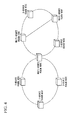
- FIG. 4 is a diagram illustrating a configuration of a photonic network.
- an optical node transmitting a signal converts the client signal to an optical signal, and transfers the converted optical signal to an optical node receiving the optical signal from the transmitting optical node, and the receiving optical node converts the optical signal to the client signal.
- a path from the transmitting node to the receiving node through which the optical signal passes is referred to as an optical bus.
- an ROADM (Reconfigurable Optical Add/Drop Multiplexer) node is used for the optical node.
- the ROADM node is a node capable of performing branching and insertion of the optical signal in units of wavelengths from a wavelength multiplexing (WDM: Wavelength Division Multiplexing) signal transferred from an adjacent ROADM node, and transferring the WDM signal to the adjacent ROADM node.
- WDM Wavelength Division Multiplexing
- a wavelength selection switch e.g., see Patent Document 1 has recently been used for the ROADM node.
- a wavelength selection switch that has been put to practical use, for example, includes nine input ports and one output port, and an interface that can set an optical signal output from the output port to any wavelength from any input port. Further, the wavelength selection switch has a function of setting an optical attenuation factor for each wavelength in order to equalize levels of the optical signals from the optical output ports.
- FIG. 5 is a diagram illustrating a configuration of an ROADM node including a wavelength selection switch.
- the ROADM node includes a wavelength selection switch (WSS) that switches a path of an optical signal, an optical amplifier, a transmitter that converts a client signal into an optical signal and transmits the optical signal, a receiver that receives the optical signal and converts the optical signal to a client signal, and an optical coupler.
- WSS wavelength selection switch
- the wavelength selection switch includes a wavelength separation element such as a diffraction grating that separates a path of a wavelength of a WDM signal from each port, and a number of movable mirrors that change the path of each wavelength. Movement of the mirror is realized through application of a voltage.
- a wavelength separation element such as a diffraction grating that separates a path of a wavelength of a WDM signal from each port, and a number of movable mirrors that change the path of each wavelength. Movement of the mirror is realized through application of a voltage.
- the wavelength selection switch needs to stably realize switching of an optical signal path in a steady state and attenuation factor adjustment for reduction of a level deviation between wavelengths at a wide range of environmental temperatures. Therefore, a control system having, for example, an external interface function for receiving control information of a relatively complicated control circuit having a temperature compensation function or the like and a wavelength selection switch, and a monitoring function of checking normality of an operation thereof is often built in the wavelength selection switch.
- FIG. 6 is a block diagram illustrating a configuration of a wavelength selection switch system.
- a wavelength selection switch system 1 includes mainly a digital circuit. Since driving of a mirror 21 in a wavelength selection switch 2 is performed through voltage control, a digital-analog conversion circuit (DAC) 32 is connected to the mirror 21 and an analog-digital conversion circuit (ADC) 33 is connected to a sensor part such as a temperature sensor 22 for temperature compensation, but all parts other than these are configured as digital circuits.
- DAC digital-analog conversion circuit
- ADC analog-digital conversion circuit
- a control circuit 31 including, for example, an FPGA (Field-Programmable Gate Array) provides instructions to calculate a driving voltage of the mirror 21 based on configuration information of the mirror 21 held in a nonvolatile memory 36 and a temperature of the wavelength selection switch from the temperature sensor 22 and to output the voltage to the DAC 32 when a supply voltage is supplied.
- FPGA Field-Programmable Gate Array
- a DAC or a plurality of DAC groups including 300 (100x3) output ports is used.
- processing operations (1) to (3) are repeated in which the control circuit 31 (1) reads mirror configuration information in the nonvolatile memory 36, (2) calculates a temperature compensation value using temperature information from the temperature sensor 22, and (3) instructs the DAC 32 to set a voltage. Further, the control circuit 31 performs rewriting of the nonvolatile memory 36 upon receiving a switch configuration instruction from an I/O port via an input and output interface 34, and controls an operation of the mirror 21 based on rewritten mirror configuration information after the rewriting.
- Patent Document 1 Japanese Unexamined Patent Application, First Publication No. 2006-86770
- the present invention has been made in view of such circumstances, and an object of the present invention is to provide a wavelength selection switch system and a method for controlling a wavelength selection switch which are capable of improving reliability of reading of configuration information.
- the present invention is characterized by including: a wavelength selection switch including an input port and an output port; a nonvolatile memory in which configuration information for controlling an operation of the wavelength selection switch is stored; a high-speed memory in which reading and writing is able to be performed at a higher speed than in the nonvolatile memory, and that stores a copy of the configuration information stored in the nonvolatile memory; and a control means that controls an operation of the wavelength selection switch based on the configuration information read from the high-speed memory, wherein the control means periodically reads the configuration information stored in the nonvolatile memory and writes a copy of the read configuration information to the high-speed memory.
- the present invention is characterized by further including: a normality confirmation means that confirms normality of data transferred between the control means and the nonvolatile memory and between the control means and the high-speed memory; a malfunction history writing means that writes malfunction history information to the nonvolatile memory when the normality is not able to be confirmed by the normality confirmation means; and a malfunction notification means which notifies the outside of information indicating occurrence of a malfunction when the normality is not able to be confirmed.
- the present invention is characterized in that the nonvolatile memory is a flash memory, and writing of the malfunction history information is performed by setting a bit of a predetermined address in the flash memory corresponding to a malfunction detection point to be 1 in advance, and setting the bit of the predetermined address to be 0 when the malfunction occurs.
- control means includes a first control circuit and a second control circuit, and when circuit information of one of the control circuits is rebuilt, the other control circuit controls the operation of the wavelength selection switch and rebuilds the circuit information of the control circuit to be rebuilt.
- the present invention is characterized by a method for controlling a wavelength selection switch system including: a wavelength selection switch including an input port and an output port; a nonvolatile memory in which configuration information for controlling an operation of the wavelength selection switch is stored; a high-speed memory in which reading and writing can be performed at a higher speed than in the nonvolatile memory, and that stores a copy of the configuration information stored in the nonvolatile memory; and a control means that controls an operation of the wavelength selection switch based on the configuration information read from the high-speed memory, wherein the method includes a step in which the control means periodically reads the configuration information stored in the nonvolatile memory and writes a copy of the read configuration information to the high-speed memory.
- the present invention is characterized by further including: a normality confirmation step for confirming normality of data transferred between the control means and the nonvolatile memory and between the control means and the high-speed memory; a malfunction history writing step for writing malfunction history information to the nonvolatile memory when the normality cannot be confirmed in the normality confirmation step; and a malfunction notification step for notifying the outside of information indicating occurrence of a malfunction when the normality cannot to be confirmed.
- the present invention is characterized in that the nonvolatile memory is a flash memory, and writing of the malfunction history information is performed by causing a bit of a predetermined address in the flash memory corresponding to a malfunction detection point to be 1 in advance, and causing the bit of the predetermined address to be 0 when the malfunction occurs.
- control means includes a first control circuit and a second control circuit
- method includes a step in which, when circuit information of one of control circuits is rebuilt, the other control circuit controls the operation of the wavelength selection switch and rebuilds the circuit information of the control circuit to be rebuilt.
- the configuration information stored in the nonvolatile memory is periodically read, the copy of the read configuration information is written to the high-speed memory, and the configuration information is read at a high speed from the high-speed memory to control the operation of the wavelength selection switch, an effect that reliability is improved in comparison with prior art can be achieved.
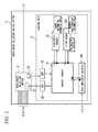
- FIG. 1 is a block diagram illustrating a configuration of the embodiment.
- the system illustrated in FIG. 1 differs from the conventional system in that a high-speed memory 35 is newly included.
- the high-speed memory is, for example, a volatile memory such as an SRAM, and is a memory faster than a nonvolatile memory 36 in reading and writing operations.
- the high-speed memory 35 is included, reading of the mirror configuration information in a nonvolatile memory in prior art is changed to reading of the mirror configuration information in the high-speed memory.
- a phenomenon called a soft error in which bit inversion occurs due to an influence of cosmic rays (e.g., neutron lines) when the high-speed memory 35 such as an SRAM is steadily used is known.
- the control circuit 31 periodically reading the mirror configuration information from the nonvolatile memory 36 such as a flash memory in which the soft error is negligible, and rewriting (copying) the mirror configuration information to the high-speed memory 35.
- a rewriting interval for example, is equal to or more than a reading interval of the mirror configuration information in the high-speed memory 35.
- the reading interval is several seconds
- the rewriting interval is several hundred seconds. Accordingly, it is possible to improve reliability since a probability of the mirror configuration information in which a soft error occurs being corrected before being read is improved.
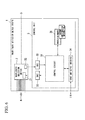
- FIG. 2 is a block diagram illustrating a configuration of the embodiment.
- the system illustrated in FIG. 2 differs from the system illustrated in FIG. 1 in that a control circuit 31 gives parity to a signal propagating through a signal line in a control unit 3 and checks when receiving the signal to detect a malfunction.
- • (black circle) indicates a parity-given point
- o (white circle) indicates a parity check point.
- malfunction history information is written to the flash memory 361 that is a nonvolatile memory.
- causes can be investigated when power is supplied after the malfunction occurs (usually, in a communication system, power is turned off when a malfunction occurs in order to perform replacement with a spare article).
- the flash memory 361 when used as a nonvolatile memory, the number of times of writing is limited and thus an idea is necessary. For example, when a malfunction such as peeling occurs in the signal line in the control unit 3, a parity error is detected each time data passes through the malfunction detection point (parity check point). If a malfunction history is written to the flash memory 361 directly after the detection, a limit of writing of the flash memory is immediately reached. In order to prevent this, when the malfunction is detected, an address in the flash memory 361 to which the malfunction history is to be written is first read. If the history has already been written, writing may not be performed. However, in order to make such a determination, a circuit scale increases and operation speed is likely to be sacrificed. Therefore, a method of preventing the sacrifice in operation speed using characteristics of the flash memory is applied.
- erasure is performed in units of blocks of the flash memory 361, all bits in the block are changed to 1, and then the data is written.
- the erasure in units of blocks in this case is limited and the number of erasures is about 100,000.
- the erasure of data is essential in writing "1" to the flash memory, but there is no limitation to change "1" to "0.”
- the flash memory 361 is subjected to block erasure, but when "0" is instructed to be written, "1" is changed to "0" only in the malfunction detection point without performing the block erasure. Therefore, a block to which the malfunction history is to be written is erased in advance, and all bits are set to be “1.” Then, when a malfunction occurs, a bit of a corresponding address of the flash memory 361 is set to be "0" to leave the malfunction history. Accordingly, a writing limitation of the flash memory 361 can be eliminated without determining whether writing is allowed.
- FIG. 3 is a block diagram illustrating a configuration of the embodiment.
- the same portions as those in the system illustrated in FIG. 2 are denoted with the same reference signs and description thereof is omitted.
- the system illustrated in FIG. 3 differs from the system illustrated in FIG. 2 in that the control circuit 31 is replaced with a first control circuit 311 and a second control circuit 312, and an output holding circuit 37 is provided between the first control circuit 311 and a DAC 32.
- the output holding circuit 37 holds an immediately previous output state during rebuilding of the first control circuit 311.
- circuit correction for a malfunction of the first control circuit 311 or circuit correction for function improvement is desired to be performed, it is difficult to perform circuit correction without affecting the optical signal passing through the wavelength selection switch 2 in the conventional wavelength selection switch system 1 and the wavelength selection switch systems 1 illustrated in Figs. 1 and 2 . Therefore, two control circuits (the first control circuit 311 and the second control circuit 312) are included and have a function of rebuilding the other control circuit. Circuit information of both the first control circuit 311 and the second control circuit 312 is held in the flash memory 361.
- the circuit information for the second control circuit 312 in the flash memory 361 is rewritten and then a rebuilding instruction is sent to the first control circuit 311.
- the first control circuit 311 resets the second control circuit 312 and writes the circuit information to perform rebuilding. Since the second control circuit 312 controls the mirror 21 of the wavelength selection switch 2 through the DAC 32, an instruction is issued so that an output is held in the output holding circuit 37 connected to the DAC 32 before the second control circuit 312 is reset.
- the output holding circuit 37 may be omitted.
- the circuit information of the first control circuit 311 and the second control circuit 312 may not be held in the flash memory 361, and a dedicated nonvolatile memory may be provided inside or outside the control unit 3.
- the number of control circuits may not be 2 but may be 3 or more, and the control circuit may include one control circuit and a rewritable ROM (read-only memory). When a ROM is used, a function unlikely to be rewritten may be stored in the ROM.
- first control circuit 311 and the second control circuit 312 one may include one control circuit having all functions and the other may include one small control circuit for holding an output to reduce costs, instead of each of the first control circuit 311 and the second control circuit 312 including a control circuit having all the functions, as illustrated in FIG. 3 .
- the wavelength selection switch 2 holds the output and does not affect a main signal even if the wavelength selection switch is not a self-holding type.
- a period of rewriting of the configuration information may be, for example, a period in which an FIT value is 100 or less based on a degree of soft error allowance, the period may be fixed, the period may be small in inverse proportion to an error occurrence probability, the period may be switched to a smaller period when the error occurrence probability exceeds a predetermined threshold, or rewriting may be performed at any time regardless of the rewriting period each time the error is detected.
- an FIT number may be enhanced as follows.
- Rewriting of the configuration information is performed in a period T 2 on a high-speed memory (SRAM) in which an average occurrence period of the soft error is T 1 .
- T 2 is determined to be 1/n of an average mirror control period. Since an error is included in data for mirror control in this condition when data is read immediately after the soft error occurs (before the configuration information is rewritten to correct the error), a probability that the soft error will occur within a certain period is T 2/ T 1 , and a probability that data will be referenced within the period is expressed using an equation below.
- T 2 / T 1 ⁇ 1 / T 2 ⁇ n 1 / T 1 ⁇ n
- the FIT number is 1/1000 of the FIT number when rewriting is not periodically performed.
- the rewriting period T 2 of the configuration information may be determined according to the FIT number per unit bit of the high-speed memory (SRAM), a memory scale, the average mirror control period, and a required FIT number.
- the wavelength selection switch system includes, in the path of the optical signal from the input port to the output port, the control circuit for setting, for each wavelength, a loss when the optical signal passes through the wavelength selection switch, the nonvolatile memory, and the high-speed memory (volatile memory) in which reading and writing of data can be performed at a higher speed than in the nonvolatile memory.
- the configuration information of the wavelength selection switch is held in the nonvolatile memory, this configuration information is copied to the high-speed memory, and the configuration information is read at a high speed.
- the wavelength selection switch can operate at a high speed and the held data is prevented from being destroyed due to an influence of cosmic rays or the like on the high-speed memory (volatile memory).
- the configuration information held in the nonvolatile memory is periodically rewritten to the high-speed memory in order to prevent a defect of the wavelength selection switch. Accordingly, it is possible to improve reliability of reading of the configuration information in comparison with a conventional wavelength selection switch.
- the configuration information used for control is copied to the high-speed memory such as an SRAM rather than the nonvolatile memory such as a flash memory and used, and the soft error with use of the high-speed memory is solved by periodical rewriting from the nonvolatile memory to the high-speed memory and parity checking. Therefore, it is possible to suppress occurrence of a soft error and a signal error caused by external noise or the like to maintain reliability while achieving a high-speed reading operation of the configuration information for control.
- ROADM Reconfigurable Optical Add/Drop Multiplexer
- this configuration is applicable to communication devices other than the wavelength selection switch, or devices other than the communication device.
- the configuration is applicable to a device necessarily requiring that the information stored in the memory can be read at a high speed and the information stored in the memory is prevented from being destroyed due to cosmic rays.
- the wavelength selection switch system according to the present invention is applicable to a device necessarily requiring that the information stored in the memory can be read at a high speed and the information stored in the memory is prevented from being destroyed due to cosmic rays or the like.
Landscapes
- Physics & Mathematics (AREA)
- Engineering & Computer Science (AREA)
- Computer Networks & Wireless Communication (AREA)
- Signal Processing (AREA)
- General Physics & Mathematics (AREA)
- Optics & Photonics (AREA)
- Optical Communication System (AREA)
- Mechanical Light Control Or Optical Switches (AREA)
Abstract
Description
- The present invention relates to a wavelength selection switch system including a wavelength selection switch used in an optical fiber communication system and its neighboring circuits, such as a control circuit, and a method of controlling a wavelength selection switch.
- Priority is claimed on Japanese Patent Application No.
2012-027248, February 10, 2012 - A photonic network including a plurality of optical nodes and optical fibers that connect the optical nodes is conventionally known.
FIG. 4 is a diagram illustrating a configuration of a photonic network. When a client signal is transferred through the photonic network, an optical node transmitting a signal converts the client signal to an optical signal, and transfers the converted optical signal to an optical node receiving the optical signal from the transmitting optical node, and the receiving optical node converts the optical signal to the client signal. A path from the transmitting node to the receiving node through which the optical signal passes is referred to as an optical bus. - In the photonic network illustrated in
FIG. 4 , an ROADM (Reconfigurable Optical Add/Drop Multiplexer) node is used for the optical node. The ROADM node is a node capable of performing branching and insertion of the optical signal in units of wavelengths from a wavelength multiplexing (WDM: Wavelength Division Multiplexing) signal transferred from an adjacent ROADM node, and transferring the WDM signal to the adjacent ROADM node. A wavelength selection switch (e.g., seePatent Document 1 has recently been used for the ROADM node. - A wavelength selection switch that has been put to practical use, for example, includes nine input ports and one output port, and an interface that can set an optical signal output from the output port to any wavelength from any input port. Further, the wavelength selection switch has a function of setting an optical attenuation factor for each wavelength in order to equalize levels of the optical signals from the optical output ports.
FIG. 5 is a diagram illustrating a configuration of an ROADM node including a wavelength selection switch. InFIG. 5 , the ROADM node includes a wavelength selection switch (WSS) that switches a path of an optical signal, an optical amplifier, a transmitter that converts a client signal into an optical signal and transmits the optical signal, a receiver that receives the optical signal and converts the optical signal to a client signal, and an optical coupler. - In an example, the wavelength selection switch includes a wavelength separation element such as a diffraction grating that separates a path of a wavelength of a WDM signal from each port, and a number of movable mirrors that change the path of each wavelength. Movement of the mirror is realized through application of a voltage.
- In this configuration, the wavelength selection switch needs to stably realize switching of an optical signal path in a steady state and attenuation factor adjustment for reduction of a level deviation between wavelengths at a wide range of environmental temperatures. Therefore, a control system having, for example, an external interface function for receiving control information of a relatively complicated control circuit having a temperature compensation function or the like and a wavelength selection switch, and a monitoring function of checking normality of an operation thereof is often built in the wavelength selection switch.
-
FIG. 6 is a block diagram illustrating a configuration of a wavelength selection switch system. In the wavelengthselection switch system 1 illustrated inFIG. 6 , an interface with the outside is a digital interface, and a wavelengthselection switch system 1 includes mainly a digital circuit. Since driving of amirror 21 in awavelength selection switch 2 is performed through voltage control, a digital-analog conversion circuit (DAC) 32 is connected to themirror 21 and an analog-digital conversion circuit (ADC) 33 is connected to a sensor part such as atemperature sensor 22 for temperature compensation, but all parts other than these are configured as digital circuits. In thecontrol unit 3 in the wavelengthselection switch system 1, acontrol circuit 31 including, for example, an FPGA (Field-Programmable Gate Array) provides instructions to calculate a driving voltage of themirror 21 based on configuration information of themirror 21 held in anonvolatile memory 36 and a temperature of the wavelength selection switch from thetemperature sensor 22 and to output the voltage to theDAC 32 when a supply voltage is supplied. - For example, in a structure in which a
mirror 21 for 100 wavelengths is included and control is performed with three electrodes per mirror, a DAC (or a plurality of DAC groups) including 300 (100x3) output ports is used. In a steady state, processing operations (1) to (3) are repeated in which the control circuit 31 (1) reads mirror configuration information in thenonvolatile memory 36, (2) calculates a temperature compensation value using temperature information from thetemperature sensor 22, and (3) instructs theDAC 32 to set a voltage. Further, thecontrol circuit 31 performs rewriting of thenonvolatile memory 36 upon receiving a switch configuration instruction from an I/O port via an input andoutput interface 34, and controls an operation of themirror 21 based on rewritten mirror configuration information after the rewriting. - [Patent Document 1] Japanese Unexamined Patent Application, First Publication No.
2006-86770 - Incidentally, in the communication system, it is very important to minimize malfunctions. However, in the wavelength
selection switch system 1 as described above, a large-scale circuit is necessary, and it is necessary to adopt a structure which increases reliability. For example, configuration information for driving themirror 21 through an I/O port is input to the input andoutput interface 34, but this information is held in thenonvolatile memory 36. It is necessary to read this configuration information at a high speed in order to frequently perform driving of themirror 21. - However, when a high-speed memory (a memory such as a volatile memory faster than a nonvolatile memory in reading and writing operations) such as an SRAM (Static Random Access Memory) from which mirror configuration information can be read at a high speed is used in place of the
nonvolatile memory 36, a soft error may be caused due to an influence of cosmic rays, and there is a problem in that a reliability degradation probability increases as a memory scale increases. Further, there is a problem in that thecontrol circuit 31 may potentially malfunction and may be likely to stop in operation since the control circuit itself is complicated. When these problems occur, it is necessary to investigate and isolate the problems to prevent the problems from recurring. However, when the communication system malfunctions, it may often be difficult to isolate a cause of the malfunction since recovery of functions of the system is preferential. - The present invention has been made in view of such circumstances, and an object of the present invention is to provide a wavelength selection switch system and a method for controlling a wavelength selection switch which are capable of improving reliability of reading of configuration information.
- The present invention is characterized by including: a wavelength selection switch including an input port and an output port; a nonvolatile memory in which configuration information for controlling an operation of the wavelength selection switch is stored; a high-speed memory in which reading and writing is able to be performed at a higher speed than in the nonvolatile memory, and that stores a copy of the configuration information stored in the nonvolatile memory; and a control means that controls an operation of the wavelength selection switch based on the configuration information read from the high-speed memory, wherein the control means periodically reads the configuration information stored in the nonvolatile memory and writes a copy of the read configuration information to the high-speed memory.
- The present invention is characterized by further including: a normality confirmation means that confirms normality of data transferred between the control means and the nonvolatile memory and between the control means and the high-speed memory; a malfunction history writing means that writes malfunction history information to the nonvolatile memory when the normality is not able to be confirmed by the normality confirmation means; and a malfunction notification means which notifies the outside of information indicating occurrence of a malfunction when the normality is not able to be confirmed.
- The present invention is characterized in that the nonvolatile memory is a flash memory, and writing of the malfunction history information is performed by setting a bit of a predetermined address in the flash memory corresponding to a malfunction detection point to be 1 in advance, and setting the bit of the predetermined address to be 0 when the malfunction occurs.
- The present invention is characterized in that the control means includes a first control circuit and a second control circuit, and when circuit information of one of the control circuits is rebuilt, the other control circuit controls the operation of the wavelength selection switch and rebuilds the circuit information of the control circuit to be rebuilt.
- The present invention is characterized by a method for controlling a wavelength selection switch system including: a wavelength selection switch including an input port and an output port; a nonvolatile memory in which configuration information for controlling an operation of the wavelength selection switch is stored; a high-speed memory in which reading and writing can be performed at a higher speed than in the nonvolatile memory, and that stores a copy of the configuration information stored in the nonvolatile memory; and a control means that controls an operation of the wavelength selection switch based on the configuration information read from the high-speed memory, wherein the method includes a step in which the control means periodically reads the configuration information stored in the nonvolatile memory and writes a copy of the read configuration information to the high-speed memory.
- The present invention is characterized by further including: a normality confirmation step for confirming normality of data transferred between the control means and the nonvolatile memory and between the control means and the high-speed memory; a malfunction history writing step for writing malfunction history information to the nonvolatile memory when the normality cannot be confirmed in the normality confirmation step; and a malfunction notification step for notifying the outside of information indicating occurrence of a malfunction when the normality cannot to be confirmed.
- The present invention is characterized in that the nonvolatile memory is a flash memory, and writing of the malfunction history information is performed by causing a bit of a predetermined address in the flash memory corresponding to a malfunction detection point to be 1 in advance, and causing the bit of the predetermined address to be 0 when the malfunction occurs.
- The present invention is characterized in that the control means includes a first control circuit and a second control circuit, and the method includes a step in which, when circuit information of one of control circuits is rebuilt, the other control circuit controls the operation of the wavelength selection switch and rebuilds the circuit information of the control circuit to be rebuilt.
- According to the present invention, since the high-speed memory in which reading and writing can be performed at a higher speed than a nonvolatile memory and that stores the copy of the configuration information stored in the nonvolatile memory is included, the configuration information stored in the nonvolatile memory is periodically read, the copy of the read configuration information is written to the high-speed memory, and the configuration information is read at a high speed from the high-speed memory to control the operation of the wavelength selection switch, an effect that reliability is improved in comparison with prior art can be achieved.
- In addition, even when a malfunction occurs, a cause can be isolated and the cause of the malfunction is easily investigated since the malfunction history information has been stored.
-
-
FIG. 1 is a block diagram illustrating a configuration of a first embodiment of the present invention. -
FIG. 2 is a block diagram illustrating a configuration of a second embodiment of the present invention. -
FIG. 3 is a block diagram illustrating a configuration of a third embodiment of the present invention. -
FIG. 4 is a diagram illustrating a configuration of a photonic network. -
FIG. 5 is a diagram illustrating a configuration of an ROADM node. -
FIG. 6 is a block diagram illustrating a configuration of a wavelength selection switch system according to prior art. - Hereinafter, a wavelength selection switch system according to a first embodiment of the present invention will be described with reference to the drawings.
FIG. 1 is a block diagram illustrating a configuration of the embodiment. InFIG. 1 , the same portions as those in a conventional system illustrated inFIG. 6 are denoted with the same reference signs and description thereof is omitted. The system illustrated inFIG. 1 differs from the conventional system in that a high-speed memory 35 is newly included. The high-speed memory is, for example, a volatile memory such as an SRAM, and is a memory faster than anonvolatile memory 36 in reading and writing operations. When the high-speed memory 35 is included, reading of the mirror configuration information in a nonvolatile memory in prior art is changed to reading of the mirror configuration information in the high-speed memory. Thus, it is possible to control themirror 21 at a high speed. - Further, a phenomenon called a soft error in which bit inversion occurs due to an influence of cosmic rays (e.g., neutron lines) when the high-
speed memory 35 such as an SRAM is steadily used is known. However, in the system illustrated inFIG. 1 , it is possible to reduce the influence of the soft error by thecontrol circuit 31 periodically reading the mirror configuration information from thenonvolatile memory 36 such as a flash memory in which the soft error is negligible, and rewriting (copying) the mirror configuration information to the high-speed memory 35. - A rewriting interval, for example, is equal to or more than a reading interval of the mirror configuration information in the high-
speed memory 35. When the reading interval is several seconds, the rewriting interval is several hundred seconds. Accordingly, it is possible to improve reliability since a probability of the mirror configuration information in which a soft error occurs being corrected before being read is improved. - Next, a wavelength selection switch system according to a second embodiment of the present invention will be described.
FIG. 2 is a block diagram illustrating a configuration of the embodiment. InFIG. 2 , the same portions as those in the system illustrated inFIG. 1 are denoted with the same reference signs and description thereof is omitted. The system illustrated inFIG. 2 differs from the system illustrated inFIG. 1 in that acontrol circuit 31 gives parity to a signal propagating through a signal line in acontrol unit 3 and checks when receiving the signal to detect a malfunction. InFIG. 2 , • (black circle) indicates a parity-given point, and o (white circle) indicates a parity check point. Furthermore, when a malfunction is detected, malfunction history information is written to theflash memory 361 that is a nonvolatile memory. By writing the malfunction history information to theflash memory 361, causes can be investigated when power is supplied after the malfunction occurs (usually, in a communication system, power is turned off when a malfunction occurs in order to perform replacement with a spare article). - However, when the
flash memory 361 is used as a nonvolatile memory, the number of times of writing is limited and thus an idea is necessary. For example, when a malfunction such as peeling occurs in the signal line in thecontrol unit 3, a parity error is detected each time data passes through the malfunction detection point (parity check point). If a malfunction history is written to theflash memory 361 directly after the detection, a limit of writing of the flash memory is immediately reached. In order to prevent this, when the malfunction is detected, an address in theflash memory 361 to which the malfunction history is to be written is first read. If the history has already been written, writing may not be performed. However, in order to make such a determination, a circuit scale increases and operation speed is likely to be sacrificed. Therefore, a method of preventing the sacrifice in operation speed using characteristics of the flash memory is applied. - When data is written to the
flash memory 361, erasure is performed in units of blocks of theflash memory 361, all bits in the block are changed to 1, and then the data is written. The erasure in units of blocks in this case is limited and the number of erasures is about 100,000. - The erasure of data is essential in writing "1" to the flash memory, but there is no limitation to change "1" to "0." When "1" is instructed to be written, the
flash memory 361 is subjected to block erasure, but when "0" is instructed to be written, "1" is changed to "0" only in the malfunction detection point without performing the block erasure. Therefore, a block to which the malfunction history is to be written is erased in advance, and all bits are set to be "1." Then, when a malfunction occurs, a bit of a corresponding address of theflash memory 361 is set to be "0" to leave the malfunction history. Accordingly, a writing limitation of theflash memory 361 can be eliminated without determining whether writing is allowed. - Next, a wavelength selection switch system according to a third embodiment of the present invention will be described.
FIG. 3 is a block diagram illustrating a configuration of the embodiment. InFIG. 3 , the same portions as those in the system illustrated inFIG. 2 are denoted with the same reference signs and description thereof is omitted. The system illustrated inFIG. 3 differs from the system illustrated inFIG. 2 in that thecontrol circuit 31 is replaced with afirst control circuit 311 and asecond control circuit 312, and anoutput holding circuit 37 is provided between thefirst control circuit 311 and aDAC 32. Theoutput holding circuit 37 holds an immediately previous output state during rebuilding of thefirst control circuit 311. - When circuit correction for a malfunction of the
first control circuit 311 or circuit correction for function improvement is desired to be performed, it is difficult to perform circuit correction without affecting the optical signal passing through thewavelength selection switch 2 in the conventional wavelengthselection switch system 1 and the wavelengthselection switch systems 1 illustrated inFigs. 1 and2 . Therefore, two control circuits (thefirst control circuit 311 and the second control circuit 312) are included and have a function of rebuilding the other control circuit. Circuit information of both thefirst control circuit 311 and thesecond control circuit 312 is held in theflash memory 361. - For example, when the
second control circuit 312 is repaired, the circuit information for thesecond control circuit 312 in theflash memory 361 is rewritten and then a rebuilding instruction is sent to thefirst control circuit 311. Thefirst control circuit 311 resets thesecond control circuit 312 and writes the circuit information to perform rebuilding. Since thesecond control circuit 312 controls themirror 21 of thewavelength selection switch 2 through theDAC 32, an instruction is issued so that an output is held in theoutput holding circuit 37 connected to theDAC 32 before thesecond control circuit 312 is reset. In addition, according to a type ofDAC 32, if the DAC has a specification that holds an immediately previous output voltage when there is no instruction, theoutput holding circuit 37 may be omitted. Further, the circuit information of thefirst control circuit 311 and thesecond control circuit 312 may not be held in theflash memory 361, and a dedicated nonvolatile memory may be provided inside or outside thecontrol unit 3. In addition, the number of control circuits may not be 2 but may be 3 or more, and the control circuit may include one control circuit and a rewritable ROM (read-only memory). When a ROM is used, a function unlikely to be rewritten may be stored in the ROM. - Further, between the
first control circuit 311 and thesecond control circuit 312, one may include one control circuit having all functions and the other may include one small control circuit for holding an output to reduce costs, instead of each of thefirst control circuit 311 and thesecond control circuit 312 including a control circuit having all the functions, as illustrated inFIG. 3 . In this case, there is an effect that, even when a large control circuit having all the functions is hung up due to an error or the like, thewavelength selection switch 2 holds the output and does not affect a main signal even if the wavelength selection switch is not a self-holding type. - Further, a period of rewriting of the configuration information may be, for example, a period in which an FIT value is 100 or less based on a degree of soft error allowance, the period may be fixed, the period may be small in inverse proportion to an error occurrence probability, the period may be switched to a smaller period when the error occurrence probability exceeds a predetermined threshold, or rewriting may be performed at any time regardless of the rewriting period each time the error is detected.
- Further, when the rewriting period for the configuration information is a period shorter than a mirror control period, an FIT number may be enhanced as follows.
- Rewriting of the configuration information is performed in a period T2 on a high-speed memory (SRAM) in which an average occurrence period of the soft error is T1. In addition, T2 is determined to be 1/n of an average mirror control period. Since an error is included in data for mirror control in this condition when data is read immediately after the soft error occurs (before the configuration information is rewritten to correct the error), a probability that the soft error will occur within a certain period is T2/T1, and a probability that data will be referenced within the period is expressed using an equation below.

- This is 1/n of 1/T1, which is an error occurrence probability when rewriting is not periodically performed. For example, if the configuration information is rewritten in a period of one second when the average mirror control period is 1000 seconds, the FIT number is 1/1000 of the FIT number when rewriting is not periodically performed. The rewriting period T2 of the configuration information may be determined according to the FIT number per unit bit of the high-speed memory (SRAM), a memory scale, the average mirror control period, and a required FIT number.
- Thus, the wavelength selection switch system according to the present invention includes, in the path of the optical signal from the input port to the output port, the control circuit for setting, for each wavelength, a loss when the optical signal passes through the wavelength selection switch, the nonvolatile memory, and the high-speed memory (volatile memory) in which reading and writing of data can be performed at a higher speed than in the nonvolatile memory. With the wavelength selection switch system according to the present invention, the configuration information of the wavelength selection switch is held in the nonvolatile memory, this configuration information is copied to the high-speed memory, and the configuration information is read at a high speed. Accordingly, the wavelength selection switch can operate at a high speed and the held data is prevented from being destroyed due to an influence of cosmic rays or the like on the high-speed memory (volatile memory). In other words, with the wavelength selection switch system according to the present invention, the configuration information held in the nonvolatile memory is periodically rewritten to the high-speed memory in order to prevent a defect of the wavelength selection switch. Accordingly, it is possible to improve reliability of reading of the configuration information in comparison with a conventional wavelength selection switch.
- As described above, in the wavelength selection switch system for an ROADM (Reconfigurable Optical Add/Drop Multiplexer), the configuration information used for control is copied to the high-speed memory such as an SRAM rather than the nonvolatile memory such as a flash memory and used, and the soft error with use of the high-speed memory is solved by periodical rewriting from the nonvolatile memory to the high-speed memory and parity checking. Therefore, it is possible to suppress occurrence of a soft error and a signal error caused by external noise or the like to maintain reliability while achieving a high-speed reading operation of the configuration information for control.
- Conventional solutions to the soft error of the configuration information include a method of correcting an error using an ECC (Error Check and Correct) memory, a method of performing majority decision from outputs of 3 redundant circuits, and the like. However, in the wavelength selection switch system described above, since a circuit and process are simple and the configuration information is periodically rewritten, an effect of a low error probability can be obtained.
- Further, while the configuration in which both the nonvolatile memory and the volatile memory are included in order to operate the
wavelength selection switch 2 at a high speed, the information stored in the memory can be read at a high speed, and the information stored in the memory can be prevented from being destroyed due to cosmic rays has been described above, this configuration is applicable to communication devices other than the wavelength selection switch, or devices other than the communication device. In other words, the configuration is applicable to a device necessarily requiring that the information stored in the memory can be read at a high speed and the information stored in the memory is prevented from being destroyed due to cosmic rays. - While the embodiments of the present invention have been described above with reference to the drawings, it is obvious that the present invention is not limited to the above embodiments. Accordingly, additions, omissions, substitutions, and other modifications of the components can be made without departing from the technical spirit and scope of the present invention.
- The wavelength selection switch system according to the present invention is applicable to a device necessarily requiring that the information stored in the memory can be read at a high speed and the information stored in the memory is prevented from being destroyed due to cosmic rays or the like.
-
- 1 wavelength selection switch system
- 2 wavelength selection switch
- 3 control unit
- 4 input port
- 5 output port
- 31 control circuit
- 32 DAC
- 33 ADC
- 34 input and output interface
- 35 high-speed memory
- 36 nonvolatile memory
- 311 first control circuit
- 312 second control circuit
- 361 flash memory
Claims (8)
- A wavelength selection switch system comprising:a wavelength selection switch including an input port and an output port;a nonvolatile memory in which configuration information for controlling an operation of the wavelength selection switch is stored;a high-speed memory in which reading and writing can be performed at a higher speed than in the nonvolatile memory, and that stores a copy of the configuration information stored in the nonvolatile memory; anda control unit that controls an operation of the wavelength selection switch based on the configuration information read from the high-speed memory,wherein the control unit periodically reads the configuration information stored in the nonvolatile memory and writes a copy of the read configuration information to the high-speed memory.
- The wavelength selection switch system according to claim 1, further comprising:a normality confirmation unit that confirms normality of data transferred between the control unit and the nonvolatile memory and between the control unit and the high-speed memory;a malfunction history writing unit that writes malfunction history information to the nonvolatile memory when the normality cannot to be confirmed by the normality confirmation unit; anda malfunction notification unit which notifies the outside of information indicating occurrence of a malfunction when the normality cannot to be confirmed.
- The wavelength selection switch system according to claim 2, wherein
the nonvolatile memory is a flash memory, and writing of the malfunction history information is performed by setting a bit of a predetermined address in the flash memory corresponding to a malfunction detection point to be 1 in advance, and setting the bit of the predetermined address to be 0 when the malfunction occurs. - The wavelength selection switch system according to any one of claims 1 to 3,
wherein the control unit includes a first control circuit and a second control circuit, and
when circuit information of the first control circuit is rebuilt, the second control circuit controls the operation of the wavelength selection switch and rebuilds the circuit information of the first control circuit to be rebuilt. - A method for controlling a wavelength selection switch system comprising:a wavelength selection switch including an input port and an output port;a nonvolatile memory in which configuration information for controlling an operation of the wavelength selection switch is stored;a high-speed memory in which reading and writing can be performed at a higher speed than in the nonvolatile memory, and that stores a copy of the configuration information stored in the nonvolatile memory; anda control unit that controls an operation of the wavelength selection switch based on the configuration information read from the high-speed memory,wherein the method includes a step in which the control unit periodically reads the configuration information stored in the nonvolatile memory and writes a copy of the read configuration information to the high-speed memory.
- The method for controlling a wavelength selection switch system according to claim 5, further comprising:a normality confirmation step for confirming normality of data transferred between the control unit and the nonvolatile memory and between the control unit and the high-speed memory;a malfunction history writing step for writing malfunction history information to the nonvolatile memory when the normality cannot be confirmed in the normality confirmation step; anda malfunction notification step for notifying the outside of information indicating occurrence of a malfunction when the normality cannot to be confirmed.
- The method for controlling a wavelength selection switch system according to claim 6, wherein the nonvolatile memory is a flash memory, and writing of the malfunction history information is performed by setting a bit of a predetermined address in the flash memory corresponding to a malfunction detection point to be 1 in advance, and setting the bit of the predetermined address to be 0 when the malfunction occurs.
- The method for controlling a wavelength selection switch system according to any one of claims 5 to 7,
wherein the control unit includes a first control circuit and a second control circuit, and
the method includes a step in which, when circuit information of the first control circuit is rebuilt, the second control circuit controls the operation of the wavelength selection switch and rebuilds the circuit information of the first control circuit to be rebuilt.
Applications Claiming Priority (2)
| Application Number | Priority Date | Filing Date | Title |
|---|---|---|---|
| JP2012027248A JP5303753B2 (en) | 2012-02-10 | 2012-02-10 | Wavelength selective switch system and method for controlling wavelength selective switch |
| PCT/JP2013/052562 WO2013118700A1 (en) | 2012-02-10 | 2013-02-05 | Wavelength selection switch system and method for controlling wavelength selection switch |
Publications (2)
| Publication Number | Publication Date |
|---|---|
| EP2811665A1 true EP2811665A1 (en) | 2014-12-10 |
| EP2811665A4 EP2811665A4 (en) | 2015-07-08 |
Family
ID=48947463
Family Applications (1)
| Application Number | Title | Priority Date | Filing Date |
|---|---|---|---|
| EP13746863.3A Withdrawn EP2811665A4 (en) | 2012-02-10 | 2013-02-05 | WAVE LENGTH SELECTION SWITCH SYSTEM AND METHOD FOR CONTROLLING WAVE LENGTH SELECTION SWITCH |
Country Status (5)
| Country | Link |
|---|---|
| US (1) | US9294826B2 (en) |
| EP (1) | EP2811665A4 (en) |
| JP (1) | JP5303753B2 (en) |
| CN (1) | CN104254986B (en) |
| WO (1) | WO2013118700A1 (en) |
Families Citing this family (8)
| Publication number | Priority date | Publication date | Assignee | Title |
|---|---|---|---|---|
| JP6337571B2 (en) * | 2014-03-28 | 2018-06-06 | 富士通株式会社 | Optical amplifier |
| US9288558B2 (en) * | 2014-03-28 | 2016-03-15 | Infinera Corporation | System for translating instructions in a switch node |
| KR102507302B1 (en) | 2018-01-22 | 2023-03-07 | 삼성전자주식회사 | Storage device and method of operating the storage device |
| CN111837348B (en) | 2018-03-13 | 2022-09-20 | 日本电气株式会社 | Optical transmission device and optical transmission method |
| CN111694782B (en) * | 2020-05-23 | 2022-03-04 | 苏州浪潮智能科技有限公司 | Device and method for realizing automatic switching of trusted platform module |
| JP7584993B2 (en) * | 2020-10-28 | 2024-11-18 | 株式会社河合楽器製作所 | Musical sound generating device and method for controlling the same |
| CN115696099A (en) * | 2021-07-26 | 2023-02-03 | 中兴通讯股份有限公司 | Service recovery method, device and computer storage medium |
| US20250119670A1 (en) * | 2023-10-05 | 2025-04-10 | Ciena Corporation | Reconfigurable mesh interconnect for hybrid electrical-optical connectivity between regional data centers |
Family Cites Families (9)
| Publication number | Priority date | Publication date | Assignee | Title |
|---|---|---|---|---|
| JP3597548B2 (en) * | 1993-11-26 | 2004-12-08 | 富士通株式会社 | Digital signal processor |
| JP2003131895A (en) * | 2001-10-29 | 2003-05-09 | Hitachi Ltd | Device with built-in memory |
| JP2006086770A (en) | 2004-09-16 | 2006-03-30 | Nikon Corp | Optical module system |
| JP4719193B2 (en) * | 2007-07-31 | 2011-07-06 | 日本電信電話株式会社 | Light switch |
| CN101222277B (en) * | 2008-02-02 | 2012-05-30 | 烽火通信科技股份有限公司 | WSS type ROADM transmission equipment and optical channel power automatic equalization method of WSS type ROADM transmission equipment |
| WO2009122516A1 (en) * | 2008-03-31 | 2009-10-08 | 富士通株式会社 | Mirror apparatus, optical switch, optical node apparatus, and mirror device controlling method |
| JP5134114B2 (en) * | 2010-05-28 | 2013-01-30 | 日本電信電話株式会社 | Wavelength selective switch and control method thereof |
| JP5213911B2 (en) | 2010-06-08 | 2013-06-19 | 株式会社日立製作所 | Optical repeater system |
| US9078054B2 (en) * | 2012-10-15 | 2015-07-07 | Sumitomo Electric Industries, Ltd. | Optical module used in optical communication systems, method of updating firmware of optical module used in optical communication systems, and trouble tracing system |
-
2012
- 2012-02-10 JP JP2012027248A patent/JP5303753B2/en active Active
-
2013
- 2013-02-05 CN CN201380008245.2A patent/CN104254986B/en active Active
- 2013-02-05 WO PCT/JP2013/052562 patent/WO2013118700A1/en not_active Ceased
- 2013-02-05 EP EP13746863.3A patent/EP2811665A4/en not_active Withdrawn
- 2013-02-05 US US14/376,786 patent/US9294826B2/en active Active
Also Published As
| Publication number | Publication date |
|---|---|
| US9294826B2 (en) | 2016-03-22 |
| JP5303753B2 (en) | 2013-10-02 |
| CN104254986A (en) | 2014-12-31 |
| CN104254986B (en) | 2016-09-07 |
| WO2013118700A1 (en) | 2013-08-15 |
| US20150030327A1 (en) | 2015-01-29 |
| EP2811665A4 (en) | 2015-07-08 |
| JP2013165386A (en) | 2013-08-22 |
Similar Documents
| Publication | Publication Date | Title |
|---|---|---|
| US9294826B2 (en) | Wavelength selection switch system and method for controlling wavelength selection switch | |
| US20170063449A1 (en) | Dynamic link repair from lane failure with minimal link down-time while sparing fault channels | |
| KR20150040537A (en) | Semiconductor memory device and semiconductor system having the same | |
| CN103731198A (en) | Optical module used in optical communication systems, method of updating firmware of optical module used in optical communication systems, and trouble tracing system | |
| CN111090545A (en) | Method, device and medium for recovering failed CPLD | |
| JP4929783B2 (en) | Power monitoring device | |
| TWI608489B (en) | Non-volatile semiconductor memory device and its test method | |
| US9053245B2 (en) | Partial redundancy for I/O modules or channels in distributed control systems | |
| JP2018181206A (en) | Data processing device, data processing method, and program | |
| JP6524126B2 (en) | Memory control device and memory control method | |
| EP2831877B1 (en) | On-the-fly trimmable sense amplifier | |
| WO2016010521A1 (en) | Partial redundancy for i/o modules or channels in distributed control systems | |
| KR101137771B1 (en) | Self-repairable digital circuit system and digital circuit self-repairing method inspired from endocrine cellular communication | |
| US20020062458A1 (en) | Semiconductor integrated circuit device | |
| KR102928888B1 (en) | Apparatus for monitoring memory state using ecc information and its method | |
| JP4351189B2 (en) | Optical transmission line monitoring method, optical transmission line monitoring program, and optical transmission line monitoring apparatus | |
| US8903248B2 (en) | Transmission apparatus and method for controlling the transmission apparatus | |
| EP0766174B1 (en) | Memory device having improved yield and reliability | |
| JP2007265056A (en) | Programmable logic device configuration device | |
| US9208040B2 (en) | Repair control logic for safe memories having redundant elements | |
| WO2014141455A1 (en) | Field-programmable gate array circuit | |
| JP5364008B2 (en) | Protective relay device | |
| JP6194679B2 (en) | Data correction circuit and data correction method | |
| WO2026042163A1 (en) | Failure monitoring device and failure monitoring method | |
| US20210319845A1 (en) | Microchip level shared array repair |
Legal Events
| Date | Code | Title | Description |
|---|---|---|---|
| PUAI | Public reference made under article 153(3) epc to a published international application that has entered the european phase |
Free format text: ORIGINAL CODE: 0009012 |
|
| 17P | Request for examination filed |
Effective date: 20140805 |
|
| AK | Designated contracting states |
Kind code of ref document: A1 Designated state(s): AL AT BE BG CH CY CZ DE DK EE ES FI FR GB GR HR HU IE IS IT LI LT LU LV MC MK MT NL NO PL PT RO RS SE SI SK SM TR |
|
| AX | Request for extension of the european patent |
Extension state: BA ME |
|
| DAX | Request for extension of the european patent (deleted) | ||
| RA4 | Supplementary search report drawn up and despatched (corrected) |
Effective date: 20150609 |
|
| RIC1 | Information provided on ipc code assigned before grant |
Ipc: G02B 26/08 20060101ALI20150602BHEP Ipc: H04B 10/03 20130101AFI20150602BHEP Ipc: H04Q 11/00 20060101ALI20150602BHEP Ipc: H04J 14/02 20060101ALI20150602BHEP Ipc: H04B 10/27 20130101ALI20150602BHEP Ipc: G06F 12/16 20060101ALI20150602BHEP |
|
| GRAP | Despatch of communication of intention to grant a patent |
Free format text: ORIGINAL CODE: EPIDOSNIGR1 |
|
| STAA | Information on the status of an ep patent application or granted ep patent |
Free format text: STATUS: GRANT OF PATENT IS INTENDED |
|
| INTG | Intention to grant announced |
Effective date: 20170816 |
|
| STAA | Information on the status of an ep patent application or granted ep patent |
Free format text: STATUS: THE APPLICATION IS DEEMED TO BE WITHDRAWN |
|
| 18D | Application deemed to be withdrawn |
Effective date: 20180103 |