EP2808708A1 - Optical element, projection optical system, and object detector - Google Patents
Optical element, projection optical system, and object detector Download PDFInfo
- Publication number
- EP2808708A1 EP2808708A1 EP14170143.3A EP14170143A EP2808708A1 EP 2808708 A1 EP2808708 A1 EP 2808708A1 EP 14170143 A EP14170143 A EP 14170143A EP 2808708 A1 EP2808708 A1 EP 2808708A1
- Authority
- EP
- European Patent Office
- Prior art keywords
- optical element
- plane
- light
- optical system
- light beam
- Prior art date
- Legal status (The legal status is an assumption and is not a legal conclusion. Google has not performed a legal analysis and makes no representation as to the accuracy of the status listed.)
- Granted
Links
Images




Classifications
-
- G—PHYSICS
- G02—OPTICS
- G02B—OPTICAL ELEMENTS, SYSTEMS OR APPARATUS
- G02B3/00—Simple or compound lenses
- G02B3/02—Simple or compound lenses with non-spherical faces
- G02B3/06—Simple or compound lenses with non-spherical faces with cylindrical or toric faces
-
- G—PHYSICS
- G02—OPTICS
- G02B—OPTICAL ELEMENTS, SYSTEMS OR APPARATUS
- G02B19/00—Condensers, e.g. light collectors or similar non-imaging optics
- G02B19/0004—Condensers, e.g. light collectors or similar non-imaging optics characterised by the optical means employed
- G02B19/0009—Condensers, e.g. light collectors or similar non-imaging optics characterised by the optical means employed having refractive surfaces only
- G02B19/0014—Condensers, e.g. light collectors or similar non-imaging optics characterised by the optical means employed having refractive surfaces only at least one surface having optical power
-
- G—PHYSICS
- G02—OPTICS
- G02B—OPTICAL ELEMENTS, SYSTEMS OR APPARATUS
- G02B19/00—Condensers, e.g. light collectors or similar non-imaging optics
- G02B19/0033—Condensers, e.g. light collectors or similar non-imaging optics characterised by the use
- G02B19/0047—Condensers, e.g. light collectors or similar non-imaging optics characterised by the use for use with a light source
- G02B19/0052—Condensers, e.g. light collectors or similar non-imaging optics characterised by the use for use with a light source the light source comprising a laser diode
-
- G—PHYSICS
- G02—OPTICS
- G02B—OPTICAL ELEMENTS, SYSTEMS OR APPARATUS
- G02B27/00—Optical systems or apparatus not provided for by any of the groups G02B1/00 - G02B26/00, G02B30/00
- G02B27/09—Beam shaping, e.g. changing the cross-sectional area, not otherwise provided for
- G02B27/0927—Systems for changing the beam intensity distribution, e.g. Gaussian to top-hat
-
- G—PHYSICS
- G02—OPTICS
- G02B—OPTICAL ELEMENTS, SYSTEMS OR APPARATUS
- G02B27/00—Optical systems or apparatus not provided for by any of the groups G02B1/00 - G02B26/00, G02B30/00
- G02B27/09—Beam shaping, e.g. changing the cross-sectional area, not otherwise provided for
- G02B27/0938—Using specific optical elements
- G02B27/095—Refractive optical elements
- G02B27/0955—Lenses
- G02B27/0966—Cylindrical lenses
-
- G—PHYSICS
- G02—OPTICS
- G02B—OPTICAL ELEMENTS, SYSTEMS OR APPARATUS
- G02B27/00—Optical systems or apparatus not provided for by any of the groups G02B1/00 - G02B26/00, G02B30/00
- G02B27/09—Beam shaping, e.g. changing the cross-sectional area, not otherwise provided for
- G02B27/0938—Using specific optical elements
- G02B27/095—Refractive optical elements
- G02B27/0972—Prisms
-
- G—PHYSICS
- G02—OPTICS
- G02B—OPTICAL ELEMENTS, SYSTEMS OR APPARATUS
- G02B5/00—Optical elements other than lenses
- G02B5/001—Axicons, waxicons, reflaxicons
Definitions
- the present invention relates to an optical element, a projection optical system that includes the optical element, and an object detector that includes the projection optical system.
- Object detectors including a light source and a projection optical system, for detecting the presence of an object and the distance between a vehicle and the object, are known.
- the projection optical system includes optical elements that alter the state of the light beam emitted from the light source, and that irradiate an object to be detected with the light beam.
- vehicle-installed laser radars are known as an example of object detectors.
- a vehicle-installed laser radar detects the presence of an object in the direction of travel of a vehicle, or detects the distance between the vehicle and the object.
- an object is irradiated with the laser light that is emitted from a light source and has passed through optical elements. Then, the light reflected or dispersed from the object is detected by a photodetector. By so doing, the laser radar detects the presence of an object existing in a specified area, or detects the distance between the vehicle and the object.
- JP-2009-103529-A discloses an example of a laser radar that is not provided with a deflector such as a rotating mirror.
- the laser radar disclosed in JP-2009-103529-A scans a specified area by alternately turning on two or more light sources that are arranged in the scanning direction.
- JP-2009-103529-A does not disclose the technique of using optical elements to irradiate a projection area with light beam having a desired intensity distribution (including even intensity distribution).
- the present invention aims at providing optical elements that irradiate a projection area with light having a desired intensity distribution.
- the present invention described herein provide an optical element including an incidence plane, and an exit plane including a plurality of planes that are jointed together.
- the incidence plane has a shape based on an angle of divergence of light beam incident upon the incidence plane and irradiation coverage of light beam exiting from the exit plane.
- a projection area can be irradiated with light having a desired intensity distribution.
- FIG. 1 is an XY-plan view of an object detector 10 according to an example embodiment of the present invention
- FIG. 2 is a ZX-plan view of the object detector 10.
- the object detector 10 includes a projection optical system 11 and a light-receptive optical system 12.
- X-axis indicates the direction in which a laser diode (LD) emits light beam (light flux), and that Y-axis and Z-axis are perpendicular to the X-axis. Moreover, it is assumed in FIG. 1 that Y-axis indicates the horizontal direction, and Z-axis indicates the vertical direction.
- LD laser diode
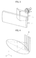
- FIG. 3 is a perspective view of the projection optical system 11.
- the projection optical system 11 according to an example embodiment of the present invention includes an LD, a first optical element L11, and a second optical element L12.
- the projection optical system 11 alters the state of the light beam emitted from the LD, and irradiates an object to be detected with the light beam.
- distance d1 between the light-emitting point of the LD and the incidence plane of the first optical element L11 is 10mm
- distance d2 between the exit plane of the first optical element L11 and the incidence plane of the second optical element L12 is 10mm.
- the size of the first optical element L11 is described below with reference to FIGS. 1 and 2 .
- the center thickness t1 is 3mm
- the edge thickness t2 is 1.1mm.
- the outer dimensions w1 in the horizontal direction is 12mm
- the outer dimensions h1 in the vertical direction is 8mm.
- the radius of curvature of the incidence plane is -10mm.
- the size of the second optical element L12 is described below with reference to FIGS. 1 and 2 .
- the center thickness t3 is 3mm
- the edge thickness t4 is 2.3mm.
- the outer dimensions w2 in the horizontal direction is 22mm
- the outer dimensions h2 in the vertical direction is 10mm.
- the radius of curvature of the exit plane is -18mm.
- the light-receptive optical system 12 includes a photodiode (PD) and a third optical element L13.
- the LD is an example of a light source according to an embodiment of the present invention.
- LDs emit light with the Gaussian intensity distribution.
- LDs have wavelength suitable for object detection, for example, an infrared area of 905nm.
- FIG. 4 is a schematic diagram of a LD according to an example embodiment of the present invention.
- the angle of divergence in the horizontal direction (Y-axis direction) is different from the angle of divergence in the vertical direction (Z-axis direction) in the LD.
- the angle of divergence in the horizontal direction (Y-axis direction) is greater than the angle of divergence in the vertical direction (Z-axis direction) in the LD.
- the angle of divergence in the horizontal direction may be less than the angle of divergence in the vertical direction (Z-axis direction) in the LD.
- the LD may include a plurality of light emitting devices or a single light emitting device.
- the first optical element L11 is an optical element according to the first embodiment of the present invention.
- the projection optical system 11 distributes the light beam emitted from the LD over irradiation coverage with even intensity distribution that is broad in the horizontal direction.
- irradiation coverage indicates an area with a specified distance from the projection optical system 11, and the area is irradiated with the light beam from the projection optical system 11 with specified light intensity.
- Even intensity distribution indicates that the dispersion of light intensity distribution is within a specified range in the irradiation coverage, and that there is no peak of light intensity.
- the first optical element L11 distribute the light beam in the horizontal direction and compensate for the shortage of light supply at an area with angle from the center (i.e., outer area of the irradiation coverage).
- FIG. 5 is an XY-plan view of an optical element according to an example embodiment of the present invention.
- the shape of the first optical element L11 is determined in view of the relationship between an irradiation area of the LD and the irradiation coverage required of the first optical element L11.
- the first optical element L11 includes an incidence plane S11 and an exit plane S12.
- the incidence plane S11 and the exit plane S12 are refractive in one direction only (in the horizontal direction only in the present embodiment).
- the incidence plane S11 and the exit plane S12 extend with the same shape in one direction (in the vertical direction in the present embodiment).
- the basic form e.g., concave surface, convex surface, and plane surface
- the profile such as radius of curvature of the incidence plane S11 are determined based on the angle of divergence of the light beam incident upon the incidence plane S11 and the irradiation coverage of the light beam exiting from the exit plane S12.
- the incidence plane S11 maybe curved to have an aspherical surface.
- the incidence plane S11 is shaped to have a concave surface opposite the LD, such that the light beam emitted from the LD is refracted to the center of light emission to compensate for shortage of light quantity in outer areas of the irradiation coverage.
- the exit plane S12 is composed of a plurality of planes (for example, two planes) that are jointed together.
- the exit plane S12 is shaped to have a gable roof where the jointed portions of the planes look like ridgelines. Due to such an arrangement, it becomes possible for the exit plane S12 to converge the light beam emitted from the LD around the center of light emission into one direction (i.e., the horizontal direction in the present embodiment).
- FIG. 6 illustrates the shape of the exit plane S12, according to an example embodiment of the present invention.
- the joint angle of the exit plane S12 is set such that the light beam incident on the joint of the two planes of the exit plane S12 from the LD irradiates the irradiation coverage at a certain distance to its edges.
- Equation 1 The shape of the exit plane S12 is expressed in Equation 1 below.
- Equation 2 the shape of the exit plane S12 can be expressed as follows.
- ⁇ tan - 1 ⁇ sin ⁇ / n - n ⁇ ⁇ cos ⁇
- Table 1 shows the relationship between the shape of the incidence plane S11 and the shape of the exit plane S12.
- the combination of the incidence plane S11 and the exit plane S12 in regard to refractive power may be selected from twelve patterns of A-X, A-Y, A-Z, B-X, B-Y, B-Z, C-X, C-Y, C-Z, D-X, D-Y, and D-Z.
- FIG. 7 is an XY-plan view illustrating an example of the shape of the second optical element L12, according to an example embodiment of the present invention.
- the second optical element L12 receives the light beam exiting from the first optical element L11, and irradiates the irradiation coverage with the light beam.
- the second optical element L12 is, for example, a cylindrical lens that is refractive such that the first optical element L11 will not be refractive.
- the second optical element L12 compensates for the lack of refractive power of the first optical element L11 such that the irradiation coverage is irradiated with the light beam of desired intensity, and adjusts the intensity distribution of light emission. For this reason, the second optical element L12 should be refractive in at least one of the horizontal and vertical directions. In FIG. 7 , the second optical element L12 is refractive in Y-direction.
- the second optical element L12 may have a different shape as long as it is shaped to compensate for the lack of refractive power of the first optical element L11 and to adjust the intensity distribution of light emission.
- the second optical element L12 has a plane surface on the incidence plane S13, and has a convex surface on the exit plane S14. Moreover, the second optical element L12 extends (sweeps) with the same shape in one direction (in the direction of Y-axis in FIG. 7 ).
- the shape of the second optical element L12 is not limited to that of the incidence plane S13 or the exit plane S14.
- the incidence plane S13 may have a concave surface.
- Table 2 depicts the relationship between shape of the first optical element L11 and the shape of the second optical element L12.
- Table 2 Optical Element First Optical Element Second Optical Element Horizontal Direction o - o - o - o Vertical Direction - o o - - o o Combination of Shape having Light-gathering Power P Q R S T U V
- the combinations of the shapes of the first optical element L11 having light-gathering power and the shapes of the second optical element L12 having light-gathering power may be selected from twelve patterns of P-T, P-U, P-V, Q-T, Q-U, Q-V, R-T, R-U, R-V, S-T, S-U, and S-V.
- FIG. 8 is a schematic diagram illustrating examples of the intensity distribution formed by the projection optical system 11, according to an example embodiment of the present invention.
- the vertical axis indicates the angle between the irradiation coverage and the center of light emission, and the vertical axis indicates the intensity of light emission.
- the projection optical system 11 may achieve uniform intensity distribution of light emission over the irradiation coverage. As depicted in (b) of FIG. 8 , the projection optical system 11 may also increase the intensity of light emission at edges of the irradiation coverage. As depicted in (c) of FIG. 8 , the projection optical system 11 may increase the intensity of light emission at a center portion of the irradiation coverage. In other words, the projection optical system 11 can achieve a desired intensity distribution like (b) and (c) of FIG. 8 depending on the configuration.
- a desired intensity distribution including uniform intensity distribution can be achieved in the irradiation coverage.
- the third optical element L13 receives the light beam that is reflected or dispersed at an object placed within the irradiation coverage, and forms an usage on the light receiving surface of a PD.
- the PD is a photodetector that receives the light beam that is reflected or dispersed at an object placed within the irradiation coverage and is shaped by the third optical element L13, and that detects the object placed within the irradiation coverage.
- the PD may be an Avalanche photodiode (APD) or a normal pin PD.
- APD Avalanche photodiode
- FIG. 9 is an XY-plan view illustrating the light-receptive area of the light-receptive optical system 12, according to an example embodiment of the present invention.
- FIG. 10 is an ZX-plan view illustrating the light-receptive area of the light-receptive optical system 12, according to an example embodiment of the present invention.
- the PD is composed of an array of photodiodes. As illustrated in FIGS. 9 and 10 , the sensor of the PD is wider in the horizontal direction than in the vertical direction. Thus, the acceptance angle (i.e., light-receptive area) is greater in the horizontal direction.
- FIG. 11 is a schematic diagram illustrating the relationship between the intensity distribution formed by the projection optical system 11 and the light-receptive area of the PD, according to an example embodiment of the present invention. As illustrated in FIG. 11 , the light-receptive area of the PD is divided into sections for each array. Accordingly, the positions of the irradiation coverage from which light is reflected can be determined.
- FIG. 12 is an XY-plan view of a projection optical system, according to an example embodiment of the present invention.
- FIG. 13 is a ZX-plan view of the projection optical system 21 of FIG. 12 .
- FIG. 14 is a perspective view of the projection optical system 21 of FIG. 12 .
- the arrangement of the first optical element L21 and the second optical element L22 in the projection optical system 21 is different from that of the projection optical system 11 described above.
- the second optical element L22 shapes the light beam emitted from the LD.
- the first optical element L21 then shapes the light beam emitted from the second optical element L22, and a desired intensity distribution including uniform intensity distribution can be achieved in the irradiation coverage.
- distance d3 between the light-emitting point of the LD and the incidence plane of the second optical element L22 is 3mm
- distance d4 between the exit plane of the second optical element L22 and the incidence plane of the first optical element L21 is 11.5mm.
- the size of the first optical element L21 is described below with reference to FIGS. 12 and 13 .
- the center thickness t6 is 4mm
- the edge thickness t7 is 2.1mm.
- the outer dimensions w4 in the horizontal direction is 14mm
- the outer dimensions h4 in the vertical direction is 6mm.
- the radius of curvature of the incidence plane is -9mm.
- the size of the second optical element L22 is described below with reference to FIGS. 12 and 13 .
- the center thickness t5 is 3.5mm
- the edge thickness t8 is 2.1mm.
- the outer dimensions w3 in the horizontal direction is 6mm
- the outer dimensions h3 in the vertical direction is 4mm.
- the radii of curvature of the exit plane are -7.5mm and -3.5mm, on the horizontal and vertical planes, respectively.
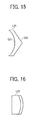
- FIG. 15 is an XY-plan view of the first optical element L21, according to an example embodiment of the present invention.
- the shape of the first optical element L21 is determined in view of the relationship between the light beam shaped by the second optical element L22 and the irradiation coverage required of the first optical element L21.
- the first optical element L21 distribute the light beam in the horizontal direction and compensate for the shortage of light quantity at an area with angle from the center (i.e., outer area of the irradiation coverage).
- the first optical element L21 includes an incidence plane S21 and an exit plane S22.
- the incidence plane S21 and the exit plane S22 have shape for changing the direction of travel of the light beam in one direction only (in the horizontal direction only in the present embodiment).
- the incidence plane S21 and the exit plane S22 extend (sweeps) with the same shape in one direction (in the vertical direction in the present embodiment).
- the basic form and the profile such as radius of curvature of the incidence plane S21 are determined based on the angle of divergence of the light beam incident upon the incidence plane S21 and the irradiation coverage of the light beam exiting from the exit plane S22.
- the incidence plane S21 may be curved to have an aspherical surface.
- the incidence plane S21 is shaped to have a concave surface opposite the second optical element L22, such that the light beam emitted from the second optical element L22 is refracted to the center of light emission to compensate for shortage of light quantity in outer areas of the irradiation coverage.
- the exit plane S22 is also composed of a plurality of planes (for example, two planes) that are jointed together. Due to such an arrangement, it becomes possible for the exit plane S22 to converge the light beam exiting from the second optical element L22 into one direction (i.e., the horizontal direction in the present embodiment).
- Equation 4 tan - 1 ⁇ sin ⁇ / n - n ⁇ ⁇ cos ⁇
- the combination of the shape of the incidence plane S21 and the shape of the exit plane S22 may be selected from twelve patterns of A-X, A-Y, A-Z, B-X, B-Y, B-Z, C-X, C-Y, C-Z, D-X, D-Y, and D-Z depicted in Table 1.
- FIG. 16 is an XY-plan view of the second optical element L22 provided for the projection optical system 21.
- the second optical element L22 receives the light beam emitted from the LD, and emits the shaped light beam to the first optical element L21.
- the second optical element L22 is, for example, a toroidal lens that is refractive in a plurality of directions. Note that the shape of the second optical element L22 is not limited to a toroidal shape, but may have a different shape as long as it is shaped to effectively deliver the light from the LD to the first optical element L21.
- the second optical element L22 compensates for the lack of refractive power of the first optical element L21 such that the irradiation coverage is irradiated with the light beam of desired intensity, and adjusts the intensity distribution of light emission. For this reason, the second optical element L22 should be refractive in both the horizontal and vertical directions.
- the second optical element L22 has a plane surface on an incidence plane S23, and has a convex surface on an exit plane S24 where the curvature in the horizontal direction is different from the curvature in the vertical direction.
- the shape of the second optical element L22 is not limited to the shape of the incidence plane S23 and the exit plane S24 described above.
- the incidence plane S23 may have a concave surface.
- Table 3 depicts the relationship between the shape of the first optical element L21 and the shape of the second optical element L22.
- Table 3 Optical Element First Optical Element Second Optical Element Horizontal Direction o - o - o - o Vertical Direction - o o - - o o Combination of shape having light-gathering power P Q R S T U V
- the combinations of the shapes of the first optical element L11 having light-gathering power and the shapes of the second optical element L12 having light-gathering power may be selected from twelve patterns of P-T, P-U, P-V, Q-T, Q-U, Q-V, R-T, R-U, R-V, S-T, S-U, and S-V.
- the projection optical system 21 may achieve uniform intensity distribution of light emission over the irradiation coverage. As depicted in (b) of FIG. 8 , the projection optical system 21 may increase the intensity of light emission at edges of the irradiation coverage. As depicted in (c) of FIG. 8 , the projection optical system 21 may increase the intensity of light emission at a center portion of the irradiation coverage. In other words, the projection optical system 21 can achieve a desired intensity distribution like (b) and (c) of FIG. 8 depending on the configuration.
- a desired intensity distribution including uniform intensity distribution can be achieved in the irradiation coverage.
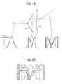
- FIG. 17 is a schematic diagram illustrating the differences between the intensity distribution of the light beam that is about to enter the first optical element L11 and the intensity distribution of the light beam that has entered the incidence plane S11. As illustrated in FIG. 17 , intensity distribution b of the light beam that has entered the incidence plane S11 has an intensity distribution of light emission with a wider angle in comparison to intensity distribution a that is about to enter the first optical element L11.
- FIG. 18 is a schematic diagram illustrating the intensity distribution of the light beam exiting from the first optical element L11. As illustrated in FIG. 18 , the light beam exiting from the first optical element L11 has intensity distribution of light emission with a wider angle. In other words, according to the first optical element L11, a desired intensity distribution can be generated by changing the light-gathering power on the incidence plane S11 to vary the light quantity around the center of light emission.
- FIG. 19 is an XY-plan view illustrating a comparative example of an optical element.
- an optical element L31 according to the comparative example has the shape of the exit plane S 12 of the first optical element L11 on the LD side.
- the incidence plane S31 of the optical element L31 has the shape of the exit plane S12 of the first optical element L11.
- the exit plane S32 of the optical element L31 has the shape of the incidence plane S11 of the first optical element L11.
- intensity distribution c of the light beam that is about to enter the first optical element L31, intensity distribution d of the light beam that has entered the incidence plane S31, and intensity distribution e of the light beam that has exited the exit plane S32 are illustrated.
- a comparison of intensity distributions c, d, and e shows an increase in intensity distribution e on the periphery of the irradiation coverage.
- FIG. 20 is a schematic diagram illustrating the intensity distribution of the light beam exiting from the optical element L31. As illustrated in FIG. 20 , the optical element L31 fails to achieve a desired intensity distribution including uniform intensity distribution in the irradiation coverage.
Landscapes
- Physics & Mathematics (AREA)
- General Physics & Mathematics (AREA)
- Optics & Photonics (AREA)
- Optical Radar Systems And Details Thereof (AREA)
- Optical Elements Other Than Lenses (AREA)
- Lenses (AREA)
Abstract
Description
- The present invention relates to an optical element, a projection optical system that includes the optical element, and an object detector that includes the projection optical system.
- Object detectors including a light source and a projection optical system, for detecting the presence of an object and the distance between a vehicle and the object, are known. The projection optical system includes optical elements that alter the state of the light beam emitted from the light source, and that irradiate an object to be detected with the light beam.
- For example, vehicle-installed laser radars are known as an example of object detectors. A vehicle-installed laser radar detects the presence of an object in the direction of travel of a vehicle, or detects the distance between the vehicle and the object.
- In such a laser radar, an object is irradiated with the laser light that is emitted from a light source and has passed through optical elements. Then, the light reflected or dispersed from the object is detected by a photodetector. By so doing, the laser radar detects the presence of an object existing in a specified area, or detects the distance between the vehicle and the object.
-
JP-2009-103529-A JP-2009-103529-A - However,
JP-2009-103529-A - The present invention aims at providing optical elements that irradiate a projection area with light having a desired intensity distribution.
- The present invention described herein provide an optical element including an incidence plane, and an exit plane including a plurality of planes that are jointed together. The incidence plane has a shape based on an angle of divergence of light beam incident upon the incidence plane and irradiation coverage of light beam exiting from the exit plane.
- According to the present invention, a projection area can be irradiated with light having a desired intensity distribution.
- A more complete appreciation of exemplary embodiments and the many attendant advantages thereof will be readily obtained as the same becomes better understood by reference to the following detailed description when considered in connection with the accompanying drawings.
-
FIG. 1 is an XY-plan view of an object detector according to an example embodiment of the present invention. -
FIG. 2 is a ZX-plan view of the object detector ofFIG. 1 , according to an example embodiment of the present invention. -
FIG. 3 is a perspective view of a projection optical system, according to an example embodiment of the present invention. -
FIG. 4 is a schematic diagram of a laser diode according to an example embodiment of the present invention. -
FIG. 5 is an XY-plan view of an optical element according to an example embodiment of the present invention. -
FIG 6 illustrates the shape of an exit plane of the optical element ofFIG. 5 , according to an example embodiment of the present invention. -
FIG. 7 is an XY-plan view illustrating an example of the shape of the second optical element, according to an example embodiment of the present invention. -
FIG. 8 is a schematic diagram illustrating examples of the intensity distribution formed by a projection optical system, according to an example embodiment of the present invention. -
FIG. 9 is an XY-plan view illustrating the light-receptive area of a light-receptive optical system of an object detector, according to an example embodiment of the present invention. -
FIG. 10 is a ZX-plan view illustrating the light-receptive area of a light-receptive optical system of an object detector, according to an example embodiment of the present invention. -
FIG. 11 is a schematic diagram illustrating the relationship between the intensity distribution formed by a projection optical system and the light-receptive area of a photodiode, according to an example embodiment of the present invention. -
FIG. 12 is an XY-plan view of a projection optical system, according to another example embodiment of the present invention. -
FIG. 13 is a ZX-plan view of the projection optical system ofFIG. 12 , according to another example embodiment of the present invention. -
FIG. 14 is a perspective view of the projection optical system ofFIG. 12 , according to another example embodiment of the present invention. -
FIG. 15 is an XY-plan view of an optical element according to another example embodiment of the present invention. -
FIG. 16 is an XY-plan view of a second optical element provided for the projection optical system ofFIG. 12 , according to another example embodiment of the present invention. -
FIG. 17 is a schematic diagram illustrating the differences between the intensity distribution of the light beam that is about to enter a first optical element provided for a projection optical system and the intensity distribution of the light beam that has entered the incidence plane of the first optical element, according to another example embodiment of the present invention. -
FIG. 18 is a schematic diagram illustrating the intensity distribution of the light beam exiting from the first optical element provided for a projection optical system, according to another example embodiment of the present invention. -
FIG. 19 is an XY-plan view illustrating a comparative example of an optical element. -
FIG. 20 is a schematic diagram illustrating the intensity distribution of the light beam exiting from the optical element ofFIG. 19 . - The accompanying drawings are intended to depict exemplary embodiments of the present disclosure and should not be interpreted to limit the scope thereof. The accompanying drawings are not to be considered as drawn to scale unless explicitly noted.
- The terminology used herein is for the purpose of describing particular embodiments only and is not intended to be limiting of the present invention. As used herein, the singular forms "a", "an" and "the" are intended to include the plural forms as well, unless the context clearly indicates otherwise. It will be further understood that the terms "includes" and/or "including", when used in this specification, specify the presence of stated features, integers, steps, operations, elements, and/or components, but do not preclude the presence or addition of one or more other features, integers, steps, operations, elements, components, and/or groups thereof.
- In describing example embodiments shown in the drawings, specific terminology is employed for the sake of clarity. However, the present disclosure is not intended to be limited to the specific terminology so selected and it is to be understood that each specific element includes all technical equivalents that have the same structure, operate in a similar manner, and achieve a similar result.
- An optical element, projection optical system, and object detector according to example embodiments of the present invention will be described below with reference to the drawings.
- Firstly, an object detector according to an example embodiment of the present invention is described.
-
FIG. 1 is an XY-plan view of anobject detector 10 according to an example embodiment of the present invention, andFIG. 2 is a ZX-plan view of theobject detector 10. As illustrated inFIGS. 1 and 2 , theobject detector 10 includes a projectionoptical system 11 and a light-receptiveoptical system 12. - In
FIG. 1 , it is assumed that X-axis indicates the direction in which a laser diode (LD) emits light beam (light flux), and that Y-axis and Z-axis are perpendicular to the X-axis. Moreover, it is assumed inFIG. 1 that Y-axis indicates the horizontal direction, and Z-axis indicates the vertical direction. -
FIG. 3 is a perspective view of the projectionoptical system 11. The projectionoptical system 11 according to an example embodiment of the present invention includes an LD, a first optical element L11, and a second optical element L12. - The projection
optical system 11 alters the state of the light beam emitted from the LD, and irradiates an object to be detected with the light beam. - The arrangement of the projection
optical system 11 is described below with reference toFIG. 1 . In the projectionoptical system 11, distance d1 between the light-emitting point of the LD and the incidence plane of the first optical element L11 is 10mm, and distance d2 between the exit plane of the first optical element L11 and the incidence plane of the second optical element L12 is 10mm. - Next, the size of the first optical element L11 is described below with reference to
FIGS. 1 and 2 . In the first optical element L11, the center thickness t1 is 3mm, and the edge thickness t2 is 1.1mm. The outer dimensions w1 in the horizontal direction is 12mm, and the outer dimensions h1 in the vertical direction is 8mm. The radius of curvature of the incidence plane is -10mm. - Next, the size of the second optical element L12 is described below with reference to
FIGS. 1 and 2 . In the second optical element L12, the center thickness t3 is 3mm, and the edge thickness t4 is 2.3mm. The outer dimensions w2 in the horizontal direction is 22mm, and the outer dimensions h2 in the vertical direction is 10mm. The radius of curvature of the exit plane is -18mm. - The light-receptive
optical system 12 includes a photodiode (PD) and a third optical element L13. - Next, the configuration of the projection
optical system 11 is described. - The LD is an example of a light source according to an embodiment of the present invention. Generally, LDs emit light with the Gaussian intensity distribution. Moreover, LDs have wavelength suitable for object detection, for example, an infrared area of 905nm.
-
FIG. 4 is a schematic diagram of a LD according to an example embodiment of the present invention. In the LD, the angle of divergence in the horizontal direction (Y-axis direction) is different from the angle of divergence in the vertical direction (Z-axis direction) in the LD. As illustrated inFIG. 4 , the angle of divergence in the horizontal direction (Y-axis direction) is greater than the angle of divergence in the vertical direction (Z-axis direction) in the LD. - However, the angle of divergence in the horizontal direction (Y-axis direction) may be less than the angle of divergence in the vertical direction (Z-axis direction) in the LD. Moreover, the LD may include a plurality of light emitting devices or a single light emitting device.
- Next, the first optical element L11 is described below. The first optical element L11 is an optical element according to the first embodiment of the present invention.
- When an object is to be detected, the projection
optical system 11 distributes the light beam emitted from the LD over irradiation coverage with even intensity distribution that is broad in the horizontal direction. Note that the term irradiation coverage indicates an area with a specified distance from the projectionoptical system 11, and the area is irradiated with the light beam from the projectionoptical system 11 with specified light intensity. - Even intensity distribution indicates that the dispersion of light intensity distribution is within a specified range in the irradiation coverage, and that there is no peak of light intensity.
- In other words, when irradiation coverage is irradiated with light beam with even intensity distribution, it is required that the first optical element L11 distribute the light beam in the horizontal direction and compensate for the shortage of light supply at an area with angle from the center (i.e., outer area of the irradiation coverage).
-
FIG. 5 is an XY-plan view of an optical element according to an example embodiment of the present invention. The shape of the first optical element L11 is determined in view of the relationship between an irradiation area of the LD and the irradiation coverage required of the first optical element L11. - The first optical element L11 includes an incidence plane S11 and an exit plane S12. Here, the incidence plane S11 and the exit plane S12 are refractive in one direction only (in the horizontal direction only in the present embodiment). In other words, the incidence plane S11 and the exit plane S12 extend with the same shape in one direction (in the vertical direction in the present embodiment).
- The basic form (e.g., concave surface, convex surface, and plane surface) and the profile such as radius of curvature of the incidence plane S11 are determined based on the angle of divergence of the light beam incident upon the incidence plane S11 and the irradiation coverage of the light beam exiting from the exit plane S12. The incidence plane S11 maybe curved to have an aspherical surface.
- The incidence plane S11 is shaped to have a concave surface opposite the LD, such that the light beam emitted from the LD is refracted to the center of light emission to compensate for shortage of light quantity in outer areas of the irradiation coverage.
- The exit plane S12 is composed of a plurality of planes (for example, two planes) that are jointed together. In other words, the exit plane S12 is shaped to have a gable roof where the jointed portions of the planes look like ridgelines. Due to such an arrangement, it becomes possible for the exit plane S12 to converge the light beam emitted from the LD around the center of light emission into one direction (i.e., the horizontal direction in the present embodiment).
-
FIG. 6 illustrates the shape of the exit plane S12, according to an example embodiment of the present invention. As illustrated inFIG. 6 , the joint angle of the exit plane S12 is set such that the light beam incident on the joint of the two planes of the exit plane S12 from the LD irradiates the irradiation coverage at a certain distance to its edges. - The shape of the exit plane S12 is expressed in
Equation 1 below.
, where α indicates the angle between each of the planes that form the exit plane and a plane perpendicular to the direction of travel of the light incident on the incidence plane, θ
indicates half the glancing angle of an end of the irradiation coverage that is away from the center of light emission by a specified distance, n indicates the reflective index of the first optical element, and n' indicates the reflective index of a medium other than the first optical element.Equation 1 is modified as follows.

- According to
Equations 
- When the medium outside the first optical element is air, the reflective index n'=1. Thus,
Equation 4 is modified as below.
- Table 1 shows the relationship between the shape of the incidence plane S11 and the shape of the exit plane S12.
- In Table 1, "o" indicates that the surface is shaped to alter the direction of travel of the light beam that has reached the incidence plane or exit plane, and "-" indicates that the surface is not shaped to alter the direction of travel of the light beam that has reached the incidence plane or exit plane. The same applies to Tables 2 and 3 described below.
[Table 1] Plane Incident Plane Exit Plane Horizontal Direction o - o - o - o Vertical Direction - o o - - o o Combination of Shape A B C D X Y Z - As shown in Table 1, it is assumed in the first optical element L11 that the combinations of shape for altering the direction of travel of the light beam incident on the incidence plane S11 are referred to as A, B, and C, and that the combinations of shape for altering the direction of travel of the light beam incident on the exit plane S12 are referred to as X, Y, and Z.
- The combination of the incidence plane S11 and the exit plane S12 in regard to refractive power may be selected from twelve patterns of A-X, A-Y, A-Z, B-X, B-Y, B-Z, C-X, C-Y, C-Z, D-X, D-Y, and D-Z.
-
FIG. 7 is an XY-plan view illustrating an example of the shape of the second optical element L12, according to an example embodiment of the present invention. The second optical element L12 receives the light beam exiting from the first optical element L11, and irradiates the irradiation coverage with the light beam. The second optical element L12 is, for example, a cylindrical lens that is refractive such that the first optical element L11 will not be refractive. - Here, the second optical element L12 compensates for the lack of refractive power of the first optical element L11 such that the irradiation coverage is irradiated with the light beam of desired intensity, and adjusts the intensity distribution of light emission. For this reason, the second optical element L12 should be refractive in at least one of the horizontal and vertical directions. In
FIG. 7 , the second optical element L12 is refractive in Y-direction. - Note that the second optical element L12 may have a different shape as long as it is shaped to compensate for the lack of refractive power of the first optical element L11 and to adjust the intensity distribution of light emission.
- The second optical element L12 has a plane surface on the incidence plane S13, and has a convex surface on the exit plane S14. Moreover, the second optical element L12 extends (sweeps) with the same shape in one direction (in the direction of Y-axis in
FIG. 7 ). - Note that the shape of the second optical element L12 is not limited to that of the incidence plane S13 or the exit plane S14. For example, the incidence plane S13 may have a concave surface.
- Table 2 depicts the relationship between shape of the first optical element L11 and the shape of the second optical element L12.
[Table 2] Optical Element First Optical Element Second Optical Element Horizontal Direction o - o - o - o Vertical Direction - o o - - o o Combination of Shape having Light-gathering Power P Q R S T U V - As shown in Table 2, it is assumed in the projection
optical system 11 that the combinations of shape having light-gathering power in the horizontal and vertical directions of the first optical element L11 are referred to as P, Q, R, and S, and that the combinations of shape having light-gathering power in the horizontal and vertical directions of the second optical element L12 are referred to as T, U, and V. - The combinations of the shapes of the first optical element L11 having light-gathering power and the shapes of the second optical element L12 having light-gathering power may be selected from twelve patterns of P-T, P-U, P-V, Q-T, Q-U, Q-V, R-T, R-U, R-V, S-T, S-U, and S-V.
-
FIG. 8 is a schematic diagram illustrating examples of the intensity distribution formed by the projectionoptical system 11, according to an example embodiment of the present invention. InFIG. 8 , the vertical axis indicates the angle between the irradiation coverage and the center of light emission, and the vertical axis indicates the intensity of light emission. - As depicted in (a) of
FIG. 8 , the projectionoptical system 11 may achieve uniform intensity distribution of light emission over the irradiation coverage. As depicted in (b) ofFIG. 8 , the projectionoptical system 11 may also increase the intensity of light emission at edges of the irradiation coverage. As depicted in (c) ofFIG. 8 , the projectionoptical system 11 may increase the intensity of light emission at a center portion of the irradiation coverage. In other words, the projectionoptical system 11 can achieve a desired intensity distribution like (b) and (c) ofFIG. 8 depending on the configuration. - According to the projection
optical system 11, a desired intensity distribution including uniform intensity distribution can be achieved in the irradiation coverage. - The third optical element L13 receives the light beam that is reflected or dispersed at an object placed within the irradiation coverage, and forms an usage on the light receiving surface of a PD.
- The PD is a photodetector that receives the light beam that is reflected or dispersed at an object placed within the irradiation coverage and is shaped by the third optical element L13, and that detects the object placed within the irradiation coverage.
- The PD may be an Avalanche photodiode (APD) or a normal pin PD.
-
FIG. 9 is an XY-plan view illustrating the light-receptive area of the light-receptiveoptical system 12, according to an example embodiment of the present invention.FIG. 10 is an ZX-plan view illustrating the light-receptive area of the light-receptiveoptical system 12, according to an example embodiment of the present invention. InFIGS. 9 and 10 , the PD is composed of an array of photodiodes. As illustrated inFIGS. 9 and 10 , the sensor of the PD is wider in the horizontal direction than in the vertical direction. Thus, the acceptance angle (i.e., light-receptive area) is greater in the horizontal direction. -
FIG. 11 is a schematic diagram illustrating the relationship between the intensity distribution formed by the projectionoptical system 11 and the light-receptive area of the PD, according to an example embodiment of the present invention. As illustrated inFIG. 11 , the light-receptive area of the PD is divided into sections for each array. Accordingly, the positions of the irradiation coverage from which light is reflected can be determined. - Next, a projection optical system according to another embodiment of the present invention is described, mainly concerning the differences from the previously described embodiment.
-
FIG. 12 is an XY-plan view of a projection optical system, according to an example embodiment of the present invention.FIG. 13 is a ZX-plan view of the projectionoptical system 21 ofFIG. 12 .FIG. 14 is a perspective view of the projectionoptical system 21 ofFIG. 12 . As illustrated inFIGS. 12 ,13, and 14 , the arrangement of the first optical element L21 and the second optical element L22 in the projectionoptical system 21 is different from that of the projectionoptical system 11 described above. - In other words, in the projection
optical system 21, the second optical element L22 shapes the light beam emitted from the LD. According to the projectionoptical system 21, the first optical element L21 then shapes the light beam emitted from the second optical element L22, and a desired intensity distribution including uniform intensity distribution can be achieved in the irradiation coverage. - The arrangement of the projection
optical system 21 is described below with reference toFIG. 12 . In the projectionoptical system 21, distance d3 between the light-emitting point of the LD and the incidence plane of the second optical element L22 is 3mm, and distance d4 between the exit plane of the second optical element L22 and the incidence plane of the first optical element L21 is 11.5mm. - Next, the size of the first optical element L21 is described below with reference to
FIGS. 12 and13 . In the first optical element L21, the center thickness t6 is 4mm, and the edge thickness t7 is 2.1mm. The outer dimensions w4 in the horizontal direction is 14mm, and the outer dimensions h4 in the vertical direction is 6mm. The radius of curvature of the incidence plane is -9mm. - Next, the size of the second optical element L22 is described below with reference to
FIGS. 12 and13 . In the second optical element L22, the center thickness t5 is 3.5mm, and the edge thickness t8 is 2.1mm. The outer dimensions w3 in the horizontal direction is 6mm, and the outer dimensions h3 in the vertical direction is 4mm. The radii of curvature of the exit plane are -7.5mm and -3.5mm, on the horizontal and vertical planes, respectively. - Next, the first optical element L21 that is an optical element according to another embodiment of the present invention is described.
-
FIG. 15 is an XY-plan view of the first optical element L21, according to an example embodiment of the present invention. The shape of the first optical element L21 is determined in view of the relationship between the light beam shaped by the second optical element L22 and the irradiation coverage required of the first optical element L21. - In other words, in a similar manner to the first optical element L11 described above, it is required that the first optical element L21 distribute the light beam in the horizontal direction and compensate for the shortage of light quantity at an area with angle from the center (i.e., outer area of the irradiation coverage).
- The first optical element L21 includes an incidence plane S21 and an exit plane S22. Here, the incidence plane S21 and the exit plane S22 have shape for changing the direction of travel of the light beam in one direction only (in the horizontal direction only in the present embodiment). In other words, the incidence plane S21 and the exit plane S22 extend (sweeps) with the same shape in one direction (in the vertical direction in the present embodiment).
- In a similar manner to the first optical element L11 described above, the basic form and the profile such as radius of curvature of the incidence plane S21 are determined based on the angle of divergence of the light beam incident upon the incidence plane S21 and the irradiation coverage of the light beam exiting from the exit plane S22. The incidence plane S21 may be curved to have an aspherical surface.
- The incidence plane S21 is shaped to have a concave surface opposite the second optical element L22, such that the light beam emitted from the second optical element L22 is refracted to the center of light emission to compensate for shortage of light quantity in outer areas of the irradiation coverage.
- In a similar manner to the first optical element L11 described above, the exit plane S22 is also composed of a plurality of planes (for example, two planes) that are jointed together. Due to such an arrangement, it becomes possible for the exit plane S22 to converge the light beam exiting from the second optical element L22 into one direction (i.e., the horizontal direction in the present embodiment).
- In a similar manner to the first optical element L11 described above, the shape of the exit plane S22 is expressed as
Equation 4 below.
- In a similar manner to the first optical element L11 described above, the combination of the shape of the incidence plane S21 and the shape of the exit plane S22 may be selected from twelve patterns of A-X, A-Y, A-Z, B-X, B-Y, B-Z, C-X, C-Y, C-Z, D-X, D-Y, and D-Z depicted in Table 1.
-
FIG. 16 is an XY-plan view of the second optical element L22 provided for the projectionoptical system 21. The second optical element L22 receives the light beam emitted from the LD, and emits the shaped light beam to the first optical element L21. The second optical element L22 is, for example, a toroidal lens that is refractive in a plurality of directions. Note that the shape of the second optical element L22 is not limited to a toroidal shape, but may have a different shape as long as it is shaped to effectively deliver the light from the LD to the first optical element L21. - Here, the second optical element L22 compensates for the lack of refractive power of the first optical element L21 such that the irradiation coverage is irradiated with the light beam of desired intensity, and adjusts the intensity distribution of light emission. For this reason, the second optical element L22 should be refractive in both the horizontal and vertical directions.
- For example, the second optical element L22 has a plane surface on an incidence plane S23, and has a convex surface on an exit plane S24 where the curvature in the horizontal direction is different from the curvature in the vertical direction.
- Note that the shape of the second optical element L22 is not limited to the shape of the incidence plane S23 and the exit plane S24 described above. For example, the incidence plane S23 may have a concave surface.
- Relationship between Shape of First Optical Element and Shape of Second Optical Element
- Table 3 depicts the relationship between the shape of the first optical element L21 and the shape of the second optical element L22.
[Table 3] Optical Element First Optical Element Second Optical Element Horizontal Direction o - o - o - o Vertical Direction - o o - - o o Combination of shape having light-gathering power P Q R S T U V - As shown in Table 3, it is assumed in the projection
optical system 21 that the combinations of shape having light-gathering power in the horizontal and vertical directions of the first optical element L21 are referred to as P, Q, R, and S, and that the combinations of shape having light-gathering power in the horizontal and vertical directions of the second optical element L22 are referred to as T, U, and V. - The combinations of the shapes of the first optical element L11 having light-gathering power and the shapes of the second optical element L12 having light-gathering power may be selected from twelve patterns of P-T, P-U, P-V, Q-T, Q-U, Q-V, R-T, R-U, R-V, S-T, S-U, and S-V.
- In a similar manner to the projection
optical system 11 described above, as depicted in (a) ofFIG. 8 , the projectionoptical system 21 may achieve uniform intensity distribution of light emission over the irradiation coverage. As depicted in (b) ofFIG. 8 , the projectionoptical system 21 may increase the intensity of light emission at edges of the irradiation coverage. As depicted in (c) ofFIG. 8 , the projectionoptical system 21 may increase the intensity of light emission at a center portion of the irradiation coverage. In other words, the projectionoptical system 21 can achieve a desired intensity distribution like (b) and (c) ofFIG. 8 depending on the configuration. - According to the projection
optical system 21, a desired intensity distribution including uniform intensity distribution can be achieved in the irradiation coverage. - Next, changes in the intensity distribution due to the shape of the incidence plane of the first optical element L11 are described.
-
FIG. 17 is a schematic diagram illustrating the differences between the intensity distribution of the light beam that is about to enter the first optical element L11 and the intensity distribution of the light beam that has entered the incidence plane S11. As illustrated inFIG. 17 , intensity distribution b of the light beam that has entered the incidence plane S11 has an intensity distribution of light emission with a wider angle in comparison to intensity distribution a that is about to enter the first optical element L11. -
FIG. 18 is a schematic diagram illustrating the intensity distribution of the light beam exiting from the first optical element L11. As illustrated inFIG. 18 , the light beam exiting from the first optical element L11 has intensity distribution of light emission with a wider angle. In other words, according to the first optical element L11, a desired intensity distribution can be generated by changing the light-gathering power on the incidence plane S11 to vary the light quantity around the center of light emission. - Next, a comparative example of an optical element according to an embodiment of the present invention is described.
-
FIG. 19 is an XY-plan view illustrating a comparative example of an optical element. As illustrated inFIG. 19 , an optical element L31 according to the comparative example has the shape of the exit plane S 12 of the first optical element L11 on the LD side. - In other words, the incidence plane S31 of the optical element L31 has the shape of the exit plane S12 of the first optical element L11. Moreover, the exit plane S32 of the optical element L31 has the shape of the incidence plane S11 of the first optical element L11.
- In
FIG. 19 , intensity distribution c of the light beam that is about to enter the first optical element L31, intensity distribution d of the light beam that has entered the incidence plane S31, and intensity distribution e of the light beam that has exited the exit plane S32 are illustrated. A comparison of intensity distributions c, d, and e shows an increase in intensity distribution e on the periphery of the irradiation coverage. -
FIG. 20 is a schematic diagram illustrating the intensity distribution of the light beam exiting from the optical element L31. As illustrated inFIG. 20 , the optical element L31 fails to achieve a desired intensity distribution including uniform intensity distribution in the irradiation coverage. - Numerous additional modifications and variations are possible in light of the above teachings. It is therefore to be understood that within the scope of the appended claims, the disclosure of the present invention may be practiced otherwise than as specifically described herein. For example, elements and/or features of different illustrative embodiments may be combined with each other and/or substituted for each other within the scope of this disclosure and appended claims.
Claims (10)
- An optical element (L11, L21) comprising:an incidence plane (S11, S21); andan exit plane (S12, S22) including a plurality of planes that are jointed together, characterized in thatthe incidence plane (S11, S21) has a shape defined based on an angle of divergence of light beam incident upon the incidence plane (S11, S21) and irradiation coverage of light beam exiting from the exit plane (S12, S22).
- The optical element (L11, L21) according to claim 1, wherein the exit plane (S12, S22) satisfies

, where α indicates an angle between each of the planes that form the exit plane (S12, S22) and a plane perpendicular to a direction of travel of light incident on the incidence plane (S11, S21), θ indicates a half-angle of the irradiation coverage, n indicates a reflective index of the optical element (L11, L21), and n' indicates a reflective index of a medium other than the optical element (L11, L21). - The optical element (L11, L21) according to claim 1 or 2, wherein the incidence plane (S11, S21) and the exit plane (S12, S22) are refractive in one direction only.
- The optical element (L11, L21) according to claim 3, wherein the incidence plane (S11, S21) and the exit plane (S12, S22) extend with a same shape in the direction that the incidence plane and the exit plane are retractive.
- A projection optical system (11, 21) comprising an optical element (L11, L21) on which light emitted from a light source (LD) is incident, the optical element (L11, L21) being the optical element (L11, L21) according to any one of claims 1 to 4.
- The projection optical system (11,21) according to claim 5, further comprising a second optical element (L12, L22) to which light emitted from the optical element (L11, L21) is incident, the second optical element (L12, L22) being refractive such that the optical element (L11, L21) is not refractive.
- The projection optical system (11, 21) according to claim 6, wherein the second optical element (L12, L22) is a cylindrical lens.
- The projection optical system (11, 21) according to claim 5, further comprising a second optical element (L12, L22) to which light emitted from the light source (LD) is incident, the second optical element (L12, L22) being refractive in a plurality of directions.
- The projection optical system (11,21) according to claim 8, wherein the second optical element (L12, L22) is a toroidal lens
- An object detector comprising:a light source (LD); anda projection optical system (11, 21) including an optical element (L11, L21) to alter a state of light beam emitted from the light source (LD), and to irradiate an object to be detected with the light beam, the projection optical system (11, 21) being the projection optical system (11,21) according to any one of claims 5 to 9.
Applications Claiming Priority (1)
| Application Number | Priority Date | Filing Date | Title |
|---|---|---|---|
| JP2013113986A JP6172448B2 (en) | 2013-05-30 | 2013-05-30 | Optical element, projection optical system, object detection device |
Publications (2)
| Publication Number | Publication Date |
|---|---|
| EP2808708A1 true EP2808708A1 (en) | 2014-12-03 |
| EP2808708B1 EP2808708B1 (en) | 2022-10-19 |
Family
ID=50943056
Family Applications (1)
| Application Number | Title | Priority Date | Filing Date |
|---|---|---|---|
| EP14170143.3A Active EP2808708B1 (en) | 2013-05-30 | 2014-05-28 | Optical element, projection optical system, and object detector |
Country Status (2)
| Country | Link |
|---|---|
| EP (1) | EP2808708B1 (en) |
| JP (1) | JP6172448B2 (en) |
Cited By (5)
| Publication number | Priority date | Publication date | Assignee | Title |
|---|---|---|---|---|
| WO2017041915A1 (en) * | 2015-09-08 | 2017-03-16 | Huf Hülsbeck & Fürst Gmbh & Co. Kg | Sensor system of a sensor device of a motor vehicle |
| US9880264B2 (en) | 2014-10-06 | 2018-01-30 | Ricoh Company, Ltd. | Projection optical system and object detection device |
| CN109521573A (en) * | 2019-01-02 | 2019-03-26 | 苏州天准科技股份有限公司 | The linear laser hot spot longitudinal light method of 3d linear laser scanning survey equipment |
| WO2020038067A1 (en) * | 2018-08-22 | 2020-02-27 | Oppo广东移动通信有限公司 | Laser projection module and control method therefor, and depth image acquisition apparatus and electronic device |
| CN111443495A (en) * | 2020-05-23 | 2020-07-24 | 江苏珠峰光电科技有限公司 | Transmission type integrator for forming uniform line light spots |
Families Citing this family (7)
| Publication number | Priority date | Publication date | Assignee | Title |
|---|---|---|---|---|
| JP2015111090A (en) | 2013-11-05 | 2015-06-18 | 株式会社リコー | Object detection device |
| JP6340851B2 (en) | 2014-03-19 | 2018-06-13 | 株式会社リコー | Object detection device and sensing device |
| JP6362027B2 (en) | 2014-05-13 | 2018-07-25 | 株式会社リコー | Object detection device and sensing device |
| JP6660584B2 (en) * | 2015-11-25 | 2020-03-11 | 株式会社リコー | Object detection device |
| JP6933045B2 (en) | 2017-08-18 | 2021-09-08 | 株式会社リコー | Object detection device, sensing device, mobile device and object detection method |
| KR102137177B1 (en) * | 2019-03-20 | 2020-07-24 | 국방과학연구소 | Beam scanning range expander and optical phased array system |
| JP7367656B2 (en) * | 2020-11-03 | 2023-10-24 | 株式会社デンソー | light detection device |
Citations (7)
| Publication number | Priority date | Publication date | Assignee | Title |
|---|---|---|---|---|
| GB482202A (en) * | 1936-09-24 | 1938-03-24 | Richard Edmund Reason | Improvements in optical scale-reading apparatus |
| US2759393A (en) * | 1952-10-25 | 1956-08-21 | Eastman Kodak Co | Optical aligners employing axicons |
| GB2220502A (en) * | 1988-07-09 | 1990-01-10 | Exitech Ltd | Excimer laser beam homogenizer system |
| US5109161A (en) * | 1989-10-14 | 1992-04-28 | Canon Kabushiki Kaisha | Light emitter and optical system for a distance measuring device |
| WO1995018984A1 (en) * | 1994-01-07 | 1995-07-13 | Coherent, Inc. | Apparatus for creating a square or rectangular laser beam with a uniform intensity profile |
| WO2004102230A1 (en) * | 2003-05-13 | 2004-11-25 | Carl Zeiss Smt Ag | Polarization-optimized axicon system, and an illuminating system for microlithographic projection system having such an axicon system |
| JP2009103529A (en) | 2007-10-22 | 2009-05-14 | Denso Corp | Laser beam irradiation device |
Family Cites Families (12)
| Publication number | Priority date | Publication date | Assignee | Title |
|---|---|---|---|---|
| US3551036A (en) * | 1965-10-25 | 1970-12-29 | Comitetul De Stat Pentru Cultu | Method and apparatus for stereoscopic photography |
| GB1549613A (en) * | 1975-12-23 | 1979-08-08 | Plessey Co Ltd | Optical system for producing an area of light of even dispersion of illumination |
| JPH0815412A (en) * | 1994-06-28 | 1996-01-19 | Nikon Corp | Beam projection optical system |
| JPH0829726A (en) * | 1994-07-13 | 1996-02-02 | Nikon Corp | Beam shaping optics |
| JPH10186115A (en) * | 1996-12-20 | 1998-07-14 | Sharp Corp | Laser beam generating optical element and laser beam generating device |
| US7167322B2 (en) * | 2005-05-03 | 2007-01-23 | Industrial Technology Research Institute | Beam shaping apparatus |
| JP4631553B2 (en) * | 2005-06-03 | 2011-02-16 | パナソニック電工株式会社 | Optical components |
| KR100624052B1 (en) * | 2005-06-22 | 2006-09-15 | 주식회사 나노포토닉스 | An optical component comprising a lens having at least one aspherical refractive surface |
| JP2008071856A (en) * | 2006-09-13 | 2008-03-27 | Epson Imaging Devices Corp | Light source, lighting device, liquid crystal device and electronic device |
| JP5799211B2 (en) * | 2009-04-24 | 2015-10-21 | パナソニックIpマネジメント株式会社 | Distance image sensor |
| RU2010147573A (en) * | 2010-11-23 | 2012-05-27 | ООО "Научно-техническое объединение "ИРЭ-Полюс" (RU) | LASER SPOT CONFIGURATOR AND METHOD OF LASER PROCESSING OF CONSTRUCTION MATERIAL ON ITS BASIS |
| US9347644B2 (en) * | 2011-04-22 | 2016-05-24 | Sharp Kabushiki Kaisha | Lens and light source unit |
-
2013
- 2013-05-30 JP JP2013113986A patent/JP6172448B2/en active Active
-
2014
- 2014-05-28 EP EP14170143.3A patent/EP2808708B1/en active Active
Patent Citations (7)
| Publication number | Priority date | Publication date | Assignee | Title |
|---|---|---|---|---|
| GB482202A (en) * | 1936-09-24 | 1938-03-24 | Richard Edmund Reason | Improvements in optical scale-reading apparatus |
| US2759393A (en) * | 1952-10-25 | 1956-08-21 | Eastman Kodak Co | Optical aligners employing axicons |
| GB2220502A (en) * | 1988-07-09 | 1990-01-10 | Exitech Ltd | Excimer laser beam homogenizer system |
| US5109161A (en) * | 1989-10-14 | 1992-04-28 | Canon Kabushiki Kaisha | Light emitter and optical system for a distance measuring device |
| WO1995018984A1 (en) * | 1994-01-07 | 1995-07-13 | Coherent, Inc. | Apparatus for creating a square or rectangular laser beam with a uniform intensity profile |
| WO2004102230A1 (en) * | 2003-05-13 | 2004-11-25 | Carl Zeiss Smt Ag | Polarization-optimized axicon system, and an illuminating system for microlithographic projection system having such an axicon system |
| JP2009103529A (en) | 2007-10-22 | 2009-05-14 | Denso Corp | Laser beam irradiation device |
Cited By (6)
| Publication number | Priority date | Publication date | Assignee | Title |
|---|---|---|---|---|
| US9880264B2 (en) | 2014-10-06 | 2018-01-30 | Ricoh Company, Ltd. | Projection optical system and object detection device |
| WO2017041915A1 (en) * | 2015-09-08 | 2017-03-16 | Huf Hülsbeck & Fürst Gmbh & Co. Kg | Sensor system of a sensor device of a motor vehicle |
| CN108139466A (en) * | 2015-09-08 | 2018-06-08 | 胡夫·许尔斯贝克和福斯特有限及两合公司 | The sensing system of the sensor device of motor vehicle |
| WO2020038067A1 (en) * | 2018-08-22 | 2020-02-27 | Oppo广东移动通信有限公司 | Laser projection module and control method therefor, and depth image acquisition apparatus and electronic device |
| CN109521573A (en) * | 2019-01-02 | 2019-03-26 | 苏州天准科技股份有限公司 | The linear laser hot spot longitudinal light method of 3d linear laser scanning survey equipment |
| CN111443495A (en) * | 2020-05-23 | 2020-07-24 | 江苏珠峰光电科技有限公司 | Transmission type integrator for forming uniform line light spots |
Also Published As
| Publication number | Publication date |
|---|---|
| JP6172448B2 (en) | 2017-08-02 |
| JP2014232265A (en) | 2014-12-11 |
| EP2808708B1 (en) | 2022-10-19 |
Similar Documents
| Publication | Publication Date | Title |
|---|---|---|
| EP2808708A1 (en) | Optical element, projection optical system, and object detector | |
| US9880264B2 (en) | Projection optical system and object detection device | |
| US9285266B2 (en) | Object detector including a light source with light emitting region of a first size in a first direction and a second size in a second direction | |
| KR101946870B1 (en) | LIDAR light-emitting system improved pattern rotation | |
| KR102235710B1 (en) | Scanning lidar having optical structures with transmission receiving single lens | |
| KR101687994B1 (en) | LIDAR light-emitting system | |
| KR102626258B1 (en) | Optical designs and detector designs for improved resolution in LiDAR systems | |
| US9316495B2 (en) | Distance measurement apparatus | |
| US10996322B2 (en) | Lidar sensor | |
| KR101850068B1 (en) | Detecting device for lidar light source without rotation | |
| US20160377706A1 (en) | Liquid crystal waveguide steered active situational awareness sensor | |
| KR20170069702A (en) | Scanning lidar having optical structures that share a transmission receiving lens | |
| KR20210124341A (en) | Light source device, detection device, and electronic device | |
| JP6584370B2 (en) | Optical radar device for vehicles | |
| US10802115B2 (en) | Light projecting and receiving device, and laser radar device provided with same | |
| JP2022522858A (en) | Optical system of lidar transmitter and receiver | |
| JP7354451B2 (en) | Transmission unit and LIDAR device with optical homogenizer | |
| CN107787426B (en) | Light module for a vehicle headlamp | |
| CN108663757B (en) | Light-emitting angle control device | |
| KR101814129B1 (en) | Optical Apparatus for Lidar System | |
| KR102435908B1 (en) | Optical system for exposing 2d light sheet and 3d light diffusion | |
| CN114488080A (en) | Light homogenizing sheet, light emitting unit for laser radar and laser radar | |
| US20220196803A1 (en) | Lidar sensor | |
| US20250164613A1 (en) | Distance measuring device | |
| US20120300489A1 (en) | Light Generator |
Legal Events
| Date | Code | Title | Description |
|---|---|---|---|
| PUAI | Public reference made under article 153(3) epc to a published international application that has entered the european phase |
Free format text: ORIGINAL CODE: 0009012 |
|
| 17P | Request for examination filed |
Effective date: 20140528 |
|
| AK | Designated contracting states |
Kind code of ref document: A1 Designated state(s): AL AT BE BG CH CY CZ DE DK EE ES FI FR GB GR HR HU IE IS IT LI LT LU LV MC MK MT NL NO PL PT RO RS SE SI SK SM TR |
|
| AX | Request for extension of the european patent |
Extension state: BA ME |
|
| STAA | Information on the status of an ep patent application or granted ep patent |
Free format text: STATUS: EXAMINATION IS IN PROGRESS |
|
| 17Q | First examination report despatched |
Effective date: 20190214 |
|
| GRAP | Despatch of communication of intention to grant a patent |
Free format text: ORIGINAL CODE: EPIDOSNIGR1 |
|
| STAA | Information on the status of an ep patent application or granted ep patent |
Free format text: STATUS: GRANT OF PATENT IS INTENDED |
|
| INTG | Intention to grant announced |
Effective date: 20220629 |
|
| GRAS | Grant fee paid |
Free format text: ORIGINAL CODE: EPIDOSNIGR3 |
|
| GRAA | (expected) grant |
Free format text: ORIGINAL CODE: 0009210 |
|
| STAA | Information on the status of an ep patent application or granted ep patent |
Free format text: STATUS: THE PATENT HAS BEEN GRANTED |
|
| AK | Designated contracting states |
Kind code of ref document: B1 Designated state(s): AL AT BE BG CH CY CZ DE DK EE ES FI FR GB GR HR HU IE IS IT LI LT LU LV MC MK MT NL NO PL PT RO RS SE SI SK SM TR |
|
| REG | Reference to a national code |
Ref country code: GB Ref legal event code: FG4D |
|
| REG | Reference to a national code |
Ref country code: CH Ref legal event code: EP |
|
| REG | Reference to a national code |
Ref country code: IE Ref legal event code: FG4D |
|
| REG | Reference to a national code |
Ref country code: DE Ref legal event code: R096 Ref document number: 602014085244 Country of ref document: DE |
|
| REG | Reference to a national code |
Ref country code: AT Ref legal event code: REF Ref document number: 1525898 Country of ref document: AT Kind code of ref document: T Effective date: 20221115 |
|
| REG | Reference to a national code |
Ref country code: LT Ref legal event code: MG9D |
|
| REG | Reference to a national code |
Ref country code: NL Ref legal event code: MP Effective date: 20221019 |
|
| REG | Reference to a national code |
Ref country code: AT Ref legal event code: MK05 Ref document number: 1525898 Country of ref document: AT Kind code of ref document: T Effective date: 20221019 |
|
| PG25 | Lapsed in a contracting state [announced via postgrant information from national office to epo] |
Ref country code: NL Free format text: LAPSE BECAUSE OF FAILURE TO SUBMIT A TRANSLATION OF THE DESCRIPTION OR TO PAY THE FEE WITHIN THE PRESCRIBED TIME-LIMIT Effective date: 20221019 |
|
| PG25 | Lapsed in a contracting state [announced via postgrant information from national office to epo] |
Ref country code: SE Free format text: LAPSE BECAUSE OF FAILURE TO SUBMIT A TRANSLATION OF THE DESCRIPTION OR TO PAY THE FEE WITHIN THE PRESCRIBED TIME-LIMIT Effective date: 20221019 Ref country code: PT Free format text: LAPSE BECAUSE OF FAILURE TO SUBMIT A TRANSLATION OF THE DESCRIPTION OR TO PAY THE FEE WITHIN THE PRESCRIBED TIME-LIMIT Effective date: 20230220 Ref country code: NO Free format text: LAPSE BECAUSE OF FAILURE TO SUBMIT A TRANSLATION OF THE DESCRIPTION OR TO PAY THE FEE WITHIN THE PRESCRIBED TIME-LIMIT Effective date: 20230119 Ref country code: LT Free format text: LAPSE BECAUSE OF FAILURE TO SUBMIT A TRANSLATION OF THE DESCRIPTION OR TO PAY THE FEE WITHIN THE PRESCRIBED TIME-LIMIT Effective date: 20221019 Ref country code: FI Free format text: LAPSE BECAUSE OF FAILURE TO SUBMIT A TRANSLATION OF THE DESCRIPTION OR TO PAY THE FEE WITHIN THE PRESCRIBED TIME-LIMIT Effective date: 20221019 Ref country code: ES Free format text: LAPSE BECAUSE OF FAILURE TO SUBMIT A TRANSLATION OF THE DESCRIPTION OR TO PAY THE FEE WITHIN THE PRESCRIBED TIME-LIMIT Effective date: 20221019 Ref country code: AT Free format text: LAPSE BECAUSE OF FAILURE TO SUBMIT A TRANSLATION OF THE DESCRIPTION OR TO PAY THE FEE WITHIN THE PRESCRIBED TIME-LIMIT Effective date: 20221019 |
|
| PG25 | Lapsed in a contracting state [announced via postgrant information from national office to epo] |
Ref country code: RS Free format text: LAPSE BECAUSE OF FAILURE TO SUBMIT A TRANSLATION OF THE DESCRIPTION OR TO PAY THE FEE WITHIN THE PRESCRIBED TIME-LIMIT Effective date: 20221019 Ref country code: PL Free format text: LAPSE BECAUSE OF FAILURE TO SUBMIT A TRANSLATION OF THE DESCRIPTION OR TO PAY THE FEE WITHIN THE PRESCRIBED TIME-LIMIT Effective date: 20221019 Ref country code: LV Free format text: LAPSE BECAUSE OF FAILURE TO SUBMIT A TRANSLATION OF THE DESCRIPTION OR TO PAY THE FEE WITHIN THE PRESCRIBED TIME-LIMIT Effective date: 20221019 Ref country code: IS Free format text: LAPSE BECAUSE OF FAILURE TO SUBMIT A TRANSLATION OF THE DESCRIPTION OR TO PAY THE FEE WITHIN THE PRESCRIBED TIME-LIMIT Effective date: 20230219 Ref country code: HR Free format text: LAPSE BECAUSE OF FAILURE TO SUBMIT A TRANSLATION OF THE DESCRIPTION OR TO PAY THE FEE WITHIN THE PRESCRIBED TIME-LIMIT Effective date: 20221019 Ref country code: GR Free format text: LAPSE BECAUSE OF FAILURE TO SUBMIT A TRANSLATION OF THE DESCRIPTION OR TO PAY THE FEE WITHIN THE PRESCRIBED TIME-LIMIT Effective date: 20230120 |
|
| P01 | Opt-out of the competence of the unified patent court (upc) registered |
Effective date: 20230525 |
|
| REG | Reference to a national code |
Ref country code: DE Ref legal event code: R097 Ref document number: 602014085244 Country of ref document: DE |
|
| PG25 | Lapsed in a contracting state [announced via postgrant information from national office to epo] |
Ref country code: SM Free format text: LAPSE BECAUSE OF FAILURE TO SUBMIT A TRANSLATION OF THE DESCRIPTION OR TO PAY THE FEE WITHIN THE PRESCRIBED TIME-LIMIT Effective date: 20221019 Ref country code: RO Free format text: LAPSE BECAUSE OF FAILURE TO SUBMIT A TRANSLATION OF THE DESCRIPTION OR TO PAY THE FEE WITHIN THE PRESCRIBED TIME-LIMIT Effective date: 20221019 Ref country code: EE Free format text: LAPSE BECAUSE OF FAILURE TO SUBMIT A TRANSLATION OF THE DESCRIPTION OR TO PAY THE FEE WITHIN THE PRESCRIBED TIME-LIMIT Effective date: 20221019 Ref country code: DK Free format text: LAPSE BECAUSE OF FAILURE TO SUBMIT A TRANSLATION OF THE DESCRIPTION OR TO PAY THE FEE WITHIN THE PRESCRIBED TIME-LIMIT Effective date: 20221019 Ref country code: CZ Free format text: LAPSE BECAUSE OF FAILURE TO SUBMIT A TRANSLATION OF THE DESCRIPTION OR TO PAY THE FEE WITHIN THE PRESCRIBED TIME-LIMIT Effective date: 20221019 |
|
| PLBE | No opposition filed within time limit |
Free format text: ORIGINAL CODE: 0009261 |
|
| STAA | Information on the status of an ep patent application or granted ep patent |
Free format text: STATUS: NO OPPOSITION FILED WITHIN TIME LIMIT |
|
| PG25 | Lapsed in a contracting state [announced via postgrant information from national office to epo] |
Ref country code: SK Free format text: LAPSE BECAUSE OF FAILURE TO SUBMIT A TRANSLATION OF THE DESCRIPTION OR TO PAY THE FEE WITHIN THE PRESCRIBED TIME-LIMIT Effective date: 20221019 Ref country code: AL Free format text: LAPSE BECAUSE OF FAILURE TO SUBMIT A TRANSLATION OF THE DESCRIPTION OR TO PAY THE FEE WITHIN THE PRESCRIBED TIME-LIMIT Effective date: 20221019 |
|
| 26N | No opposition filed |
Effective date: 20230720 |
|
| PG25 | Lapsed in a contracting state [announced via postgrant information from national office to epo] |
Ref country code: SI Free format text: LAPSE BECAUSE OF FAILURE TO SUBMIT A TRANSLATION OF THE DESCRIPTION OR TO PAY THE FEE WITHIN THE PRESCRIBED TIME-LIMIT Effective date: 20221019 |
|
| REG | Reference to a national code |
Ref country code: CH Ref legal event code: PL |
|
| PG25 | Lapsed in a contracting state [announced via postgrant information from national office to epo] |
Ref country code: MC Free format text: LAPSE BECAUSE OF FAILURE TO SUBMIT A TRANSLATION OF THE DESCRIPTION OR TO PAY THE FEE WITHIN THE PRESCRIBED TIME-LIMIT Effective date: 20221019 |
|
| REG | Reference to a national code |
Ref country code: BE Ref legal event code: MM Effective date: 20230531 |
|
| PG25 | Lapsed in a contracting state [announced via postgrant information from national office to epo] |
Ref country code: MC Free format text: LAPSE BECAUSE OF FAILURE TO SUBMIT A TRANSLATION OF THE DESCRIPTION OR TO PAY THE FEE WITHIN THE PRESCRIBED TIME-LIMIT Effective date: 20221019 Ref country code: LU Free format text: LAPSE BECAUSE OF NON-PAYMENT OF DUE FEES Effective date: 20230528 Ref country code: LI Free format text: LAPSE BECAUSE OF NON-PAYMENT OF DUE FEES Effective date: 20230531 Ref country code: CH Free format text: LAPSE BECAUSE OF NON-PAYMENT OF DUE FEES Effective date: 20230531 |
|
| REG | Reference to a national code |
Ref country code: IE Ref legal event code: MM4A |
|
| PG25 | Lapsed in a contracting state [announced via postgrant information from national office to epo] |
Ref country code: IE Free format text: LAPSE BECAUSE OF NON-PAYMENT OF DUE FEES Effective date: 20230528 |
|
| PG25 | Lapsed in a contracting state [announced via postgrant information from national office to epo] |
Ref country code: IE Free format text: LAPSE BECAUSE OF NON-PAYMENT OF DUE FEES Effective date: 20230528 |
|
| PG25 | Lapsed in a contracting state [announced via postgrant information from national office to epo] |
Ref country code: IT Free format text: LAPSE BECAUSE OF FAILURE TO SUBMIT A TRANSLATION OF THE DESCRIPTION OR TO PAY THE FEE WITHIN THE PRESCRIBED TIME-LIMIT Effective date: 20221019 Ref country code: BE Free format text: LAPSE BECAUSE OF NON-PAYMENT OF DUE FEES Effective date: 20230531 |
|
| PG25 | Lapsed in a contracting state [announced via postgrant information from national office to epo] |
Ref country code: BG Free format text: LAPSE BECAUSE OF FAILURE TO SUBMIT A TRANSLATION OF THE DESCRIPTION OR TO PAY THE FEE WITHIN THE PRESCRIBED TIME-LIMIT Effective date: 20221019 |
|
| PG25 | Lapsed in a contracting state [announced via postgrant information from national office to epo] |
Ref country code: BG Free format text: LAPSE BECAUSE OF FAILURE TO SUBMIT A TRANSLATION OF THE DESCRIPTION OR TO PAY THE FEE WITHIN THE PRESCRIBED TIME-LIMIT Effective date: 20221019 |
|
| PGFP | Annual fee paid to national office [announced via postgrant information from national office to epo] |
Ref country code: DE Payment date: 20250521 Year of fee payment: 12 |
|
| PGFP | Annual fee paid to national office [announced via postgrant information from national office to epo] |
Ref country code: GB Payment date: 20250521 Year of fee payment: 12 |
|
| PGFP | Annual fee paid to national office [announced via postgrant information from national office to epo] |
Ref country code: FR Payment date: 20250528 Year of fee payment: 12 |
|
| PG25 | Lapsed in a contracting state [announced via postgrant information from national office to epo] |
Ref country code: CY Free format text: LAPSE BECAUSE OF FAILURE TO SUBMIT A TRANSLATION OF THE DESCRIPTION OR TO PAY THE FEE WITHIN THE PRESCRIBED TIME-LIMIT; INVALID AB INITIO Effective date: 20140528 |
|
| PG25 | Lapsed in a contracting state [announced via postgrant information from national office to epo] |
Ref country code: HU Free format text: LAPSE BECAUSE OF FAILURE TO SUBMIT A TRANSLATION OF THE DESCRIPTION OR TO PAY THE FEE WITHIN THE PRESCRIBED TIME-LIMIT; INVALID AB INITIO Effective date: 20140528 |
|
| PG25 | Lapsed in a contracting state [announced via postgrant information from national office to epo] |
Ref country code: TR Free format text: LAPSE BECAUSE OF FAILURE TO SUBMIT A TRANSLATION OF THE DESCRIPTION OR TO PAY THE FEE WITHIN THE PRESCRIBED TIME-LIMIT Effective date: 20221019 |