EP2808056B1 - Optical stimulation device - Google Patents
Optical stimulation device Download PDFInfo
- Publication number
- EP2808056B1 EP2808056B1 EP13169700.5A EP13169700A EP2808056B1 EP 2808056 B1 EP2808056 B1 EP 2808056B1 EP 13169700 A EP13169700 A EP 13169700A EP 2808056 B1 EP2808056 B1 EP 2808056B1
- Authority
- EP
- European Patent Office
- Prior art keywords
- support
- optical
- stimulation device
- neuron
- stimulation
- Prior art date
- Legal status (The legal status is an assumption and is not a legal conclusion. Google has not performed a legal analysis and makes no representation as to the accuracy of the status listed.)
- Active
Links
- 230000003287 optical effect Effects 0.000 title claims description 115
- 230000000638 stimulation Effects 0.000 title claims description 44
- 239000000523 sample Substances 0.000 claims description 74
- XUIMIQQOPSSXEZ-UHFFFAOYSA-N Silicon Chemical compound [Si] XUIMIQQOPSSXEZ-UHFFFAOYSA-N 0.000 claims description 8
- 229910052710 silicon Inorganic materials 0.000 claims description 8
- 239000010703 silicon Substances 0.000 claims description 8
- 239000000758 substrate Substances 0.000 claims description 6
- 230000008878 coupling Effects 0.000 claims description 4
- 238000010168 coupling process Methods 0.000 claims description 4
- 238000005859 coupling reaction Methods 0.000 claims description 4
- 239000013013 elastic material Substances 0.000 claims description 4
- 210000004027 cell Anatomy 0.000 description 16
- 230000008901 benefit Effects 0.000 description 15
- 210000004556 brain Anatomy 0.000 description 14
- 239000013307 optical fiber Substances 0.000 description 12
- 210000002569 neuron Anatomy 0.000 description 7
- 239000002184 metal Substances 0.000 description 5
- 229910052751 metal Inorganic materials 0.000 description 5
- 238000001727 in vivo Methods 0.000 description 4
- 238000005286 illumination Methods 0.000 description 3
- 238000000338 in vitro Methods 0.000 description 3
- 238000000034 method Methods 0.000 description 3
- 230000000694 effects Effects 0.000 description 2
- 238000010438 heat treatment Methods 0.000 description 2
- 238000003780 insertion Methods 0.000 description 2
- 230000037431 insertion Effects 0.000 description 2
- 239000011810 insulating material Substances 0.000 description 2
- 230000000451 tissue damage Effects 0.000 description 2
- 231100000827 tissue damage Toxicity 0.000 description 2
- 239000002131 composite material Substances 0.000 description 1
- 239000000835 fiber Substances 0.000 description 1
- 239000000463 material Substances 0.000 description 1
- 230000001537 neural effect Effects 0.000 description 1
- 210000000056 organ Anatomy 0.000 description 1
- 230000037361 pathway Effects 0.000 description 1
- 229920000642 polymer Polymers 0.000 description 1
- 238000007781 pre-processing Methods 0.000 description 1
- 230000008569 process Effects 0.000 description 1
- 239000004065 semiconductor Substances 0.000 description 1
- 238000005389 semiconductor device fabrication Methods 0.000 description 1
- 230000008685 targeting Effects 0.000 description 1
Images


Classifications
-
- A—HUMAN NECESSITIES
- A61—MEDICAL OR VETERINARY SCIENCE; HYGIENE
- A61B—DIAGNOSIS; SURGERY; IDENTIFICATION
- A61B5/00—Measuring for diagnostic purposes; Identification of persons
- A61B5/24—Detecting, measuring or recording bioelectric or biomagnetic signals of the body or parts thereof
-
- A—HUMAN NECESSITIES
- A61—MEDICAL OR VETERINARY SCIENCE; HYGIENE
- A61B—DIAGNOSIS; SURGERY; IDENTIFICATION
- A61B5/00—Measuring for diagnostic purposes; Identification of persons
- A61B5/40—Detecting, measuring or recording for evaluating the nervous system
- A61B5/4058—Detecting, measuring or recording for evaluating the nervous system for evaluating the central nervous system
- A61B5/4064—Evaluating the brain
-
- A—HUMAN NECESSITIES
- A61—MEDICAL OR VETERINARY SCIENCE; HYGIENE
- A61N—ELECTROTHERAPY; MAGNETOTHERAPY; RADIATION THERAPY; ULTRASOUND THERAPY
- A61N5/00—Radiation therapy
- A61N5/06—Radiation therapy using light
- A61N5/0601—Apparatus for use inside the body
-
- A—HUMAN NECESSITIES
- A61—MEDICAL OR VETERINARY SCIENCE; HYGIENE
- A61N—ELECTROTHERAPY; MAGNETOTHERAPY; RADIATION THERAPY; ULTRASOUND THERAPY
- A61N5/00—Radiation therapy
- A61N5/06—Radiation therapy using light
- A61N5/0613—Apparatus adapted for a specific treatment
- A61N5/0622—Optical stimulation for exciting neural tissue
-
- G—PHYSICS
- G01—MEASURING; TESTING
- G01N—INVESTIGATING OR ANALYSING MATERIALS BY DETERMINING THEIR CHEMICAL OR PHYSICAL PROPERTIES
- G01N33/00—Investigating or analysing materials by specific methods not covered by groups G01N1/00 - G01N31/00
- G01N33/48—Biological material, e.g. blood, urine; Haemocytometers
- G01N33/50—Chemical analysis of biological material, e.g. blood, urine; Testing involving biospecific ligand binding methods; Immunological testing
- G01N33/5005—Chemical analysis of biological material, e.g. blood, urine; Testing involving biospecific ligand binding methods; Immunological testing involving human or animal cells
- G01N33/5091—Chemical analysis of biological material, e.g. blood, urine; Testing involving biospecific ligand binding methods; Immunological testing involving human or animal cells for testing the pathological state of an organism
-
- A—HUMAN NECESSITIES
- A61—MEDICAL OR VETERINARY SCIENCE; HYGIENE
- A61B—DIAGNOSIS; SURGERY; IDENTIFICATION
- A61B2562/00—Details of sensors; Constructional details of sensor housings or probes; Accessories for sensors
- A61B2562/16—Details of sensor housings or probes; Details of structural supports for sensors
- A61B2562/164—Details of sensor housings or probes; Details of structural supports for sensors the sensor is mounted in or on a conformable substrate or carrier
-
- A—HUMAN NECESSITIES
- A61—MEDICAL OR VETERINARY SCIENCE; HYGIENE
- A61B—DIAGNOSIS; SURGERY; IDENTIFICATION
- A61B2562/00—Details of sensors; Constructional details of sensor housings or probes; Accessories for sensors
- A61B2562/16—Details of sensor housings or probes; Details of structural supports for sensors
- A61B2562/166—Details of sensor housings or probes; Details of structural supports for sensors the sensor is mounted on a specially adapted printed circuit board
-
- A—HUMAN NECESSITIES
- A61—MEDICAL OR VETERINARY SCIENCE; HYGIENE
- A61B—DIAGNOSIS; SURGERY; IDENTIFICATION
- A61B5/00—Measuring for diagnostic purposes; Identification of persons
- A61B5/40—Detecting, measuring or recording for evaluating the nervous system
-
- A—HUMAN NECESSITIES
- A61—MEDICAL OR VETERINARY SCIENCE; HYGIENE
- A61B—DIAGNOSIS; SURGERY; IDENTIFICATION
- A61B5/00—Measuring for diagnostic purposes; Identification of persons
- A61B5/68—Arrangements of detecting, measuring or recording means, e.g. sensors, in relation to patient
- A61B5/6846—Arrangements of detecting, measuring or recording means, e.g. sensors, in relation to patient specially adapted to be brought in contact with an internal body part, i.e. invasive
- A61B5/6867—Arrangements of detecting, measuring or recording means, e.g. sensors, in relation to patient specially adapted to be brought in contact with an internal body part, i.e. invasive specially adapted to be attached or implanted in a specific body part
- A61B5/6868—Brain
-
- A—HUMAN NECESSITIES
- A61—MEDICAL OR VETERINARY SCIENCE; HYGIENE
- A61N—ELECTROTHERAPY; MAGNETOTHERAPY; RADIATION THERAPY; ULTRASOUND THERAPY
- A61N1/00—Electrotherapy; Circuits therefor
- A61N1/02—Details
- A61N1/04—Electrodes
- A61N1/05—Electrodes for implantation or insertion into the body, e.g. heart electrode
- A61N1/0526—Head electrodes
- A61N1/0529—Electrodes for brain stimulation
-
- A—HUMAN NECESSITIES
- A61—MEDICAL OR VETERINARY SCIENCE; HYGIENE
- A61N—ELECTROTHERAPY; MAGNETOTHERAPY; RADIATION THERAPY; ULTRASOUND THERAPY
- A61N1/00—Electrotherapy; Circuits therefor
- A61N1/02—Details
- A61N1/04—Electrodes
- A61N1/05—Electrodes for implantation or insertion into the body, e.g. heart electrode
- A61N1/0551—Spinal or peripheral nerve electrodes
-
- A—HUMAN NECESSITIES
- A61—MEDICAL OR VETERINARY SCIENCE; HYGIENE
- A61N—ELECTROTHERAPY; MAGNETOTHERAPY; RADIATION THERAPY; ULTRASOUND THERAPY
- A61N5/00—Radiation therapy
- A61N5/06—Radiation therapy using light
- A61N2005/0632—Constructional aspects of the apparatus
-
- A—HUMAN NECESSITIES
- A61—MEDICAL OR VETERINARY SCIENCE; HYGIENE
- A61N—ELECTROTHERAPY; MAGNETOTHERAPY; RADIATION THERAPY; ULTRASOUND THERAPY
- A61N5/00—Radiation therapy
- A61N5/06—Radiation therapy using light
- A61N2005/0635—Radiation therapy using light characterised by the body area to be irradiated
- A61N2005/0643—Applicators, probes irradiating specific body areas in close proximity
Definitions
- the invention is related to devices for the stimulation of cells.
- the invention is related to compact and reusable neuro-stimuiation devices for the optical stimulation of biological cells such as nervous tissue.
- the invention is related to in-vivo and in-vitro devices for such purposes.
- Optical stimulation of neurons in the brain based on optogenetic targeting of specific neurons is the next big thing in neuroscience.
- the technique makes it possible to stimulate specific neurons by light of a certain wavelength.
- Different stimulation devices are on the market today. However, these devices have some limitations.
- a first group of state of the art stimulation devices uses probes with optical stimulation sites located on the probes, optically connected to optical fibers. These probes are inserted in the brain and the optical stimulation sites are used to stimulate particular areas of the brain. To couple light into the probe, optical fibers are attached to the probe.
- the use of optical fibers poses problems as they are bulky.
- a first problem is the compactness of the device which is reduced due to the attachment of optical fibers to a probe. The problem increases when multiple optical fibers are connected to the probe to stimulate nervous tissue with light of multiple wavelengths.
- a second problem is the connectivity between the probe and the optical fiber. It requires a special connection in order to couple light efficiently in the probe (e.g. the angle in which the light enters the probe needs to be correct). Thus, specific, bulky connectors are necessary which increase the size and the cost of the device.
- a second group of state of the art stimulation devices uses probes with optical sources positioned on the probes.
- the light of the optical source is coupled into the probes to stimulate specific regions of the brain.
- the problem with these devices is undesired heating, which is generated by the optical source.
- the optical sources are positioned on the probes, the neurprobes tend to heat up.
- nervous tissue near the probe tends to heat up, resulting in tissue damage and unwanted side effects.
- optical neural stimulation devices A different issue which arises with current state of the art optical neural stimulation devices is the reusability factor.
- Current optical probes are usually used only once and cannot be reused. After stimulation, the probe is disposed.
- US Patent Application 2011/0122366 A1 describes a single-fiber multi-spot laser probe for ophthalmic endoiliumination.
- the ophthalmic endoilluminator includes a light source, a first optical assembly, an optical coupling element, and an optical fiber having an optical grating located distally on the optical fiber, the optical fiber optically coupled to the optical coupling element.
- a neuro-stimulation device is presented according to claim 1.
- the neuroprobe may further comprises: a tip; a shaft comprising at least one electrode and at least one optical stimulation site which is optically connected to the at least one grating coupler; and wherein the at least one grating coupler is mounted on a head which is mounted on the first support and the head further comprises at least one bondpad electrically connected to the at least one electrode. While only the head of the probe is mounted to the first support, the shaft of the probe may be inserted in the human body or brain while the rest of the device remains outside of the body. As an advantage, this allows the device to be used as an in-vivo device.
- the neuroprobe may further comprises: a silicon substrate; an interconnection layer; at least one electrode electrically connected to at least one bondpad via the interconnection layer; at least one optical stimulation site optically connected to the at least one grating coupler via the interconnection layer.
- the device allows cells or tissue to be placed on top of the probe for stimulation or recording purposes.
- the device may be used as an in-vitro device.
- the first support may further comprises an electrical connector which is electrically connected to at least one bondpad of the probe.
- the electrical connector allows the probe to be connected to another device for read-out of electrical signals from the probe.
- the second support may further comprises an optical connector electrically connected to the at least one optical source for powering and/or controlling the at least one optical source.
- the optical connector allows connecting the at least one optical source to an external device for controlling the at least one optical source.
- the at least one means for detachably attaching the first support to the second support is a bolt and a nut.
- the first or the second support may further comprises at least one guiding means for aligning the position of the at least one grating coupler with the position of the at least one optical source.
- the at least one guiding means is used to align the first support with the second support to align the position of the at least one grating coupler with the position of the at least one optical source.
- the device further comprises an interface fitting located in between the first support and the second support; the interface fitting comprising at least one through-hole aligned on one side of the interface fitting with one of the at least one grating coupler and on the other side of the interface fitting with one of the at least one optical source .
- the interface fitting is used to align grating couplers with optical sources on a one-to-one basis to avoid cross-illumination between optical sources. As an advantage, multiple optical sources may be used.
- the interface fitting features a cut-out for providing space for bond wires on the first support.
- the cut-out provides space e.g. for bond wires which may present on the first support.
- the first support may be attached to the second support in a very compact manner.
- the device further comprises a gasket fitting located in between the first support and the second support; the gasket fitting comprising at least one through-hole aligned on one side of the gasket fitting with one of the at least one grating coupler and on the other side of the gasket fitting with one of the at least one optical source.
- the gasket fitting ensures a perfect fitting between the interface fitting and the second support.
- the neuroprobe is glued to the first support.
- the first support and/or the second support and/or the interface fitting are printed circuit boards.
- the gasket fitting is fabricated from an elastic material. Due to the elastic material the gasket fitting is flexible. As an advantage, a perfect and tight fitting between the interface fitting and the second support is possible.
- the at least one optical source is a LED.
- the neuron-stimulation device may be used as a bio-probe, a neuroprobe or a biosensor.
- the neuron-stimulation device may be used for the stimulation of biological cells such as neurons in the brain, biological cells in the body.
- a PCB this is defined as a printed circuit board.
- a printed circuit board is used to mechanically support and electrically connect electronic components using conductive pathways, tracks or signal traces etched from e.g. copper sheets laminated onto a non-conductive substrate.
- a bondpad this is defined as an electrically conductive, e.g. metallized, area on a surface of a semiconductor device to which connections can be made.
- wire bonding this is defined as a technique for making interconnections between an integrated circuit (IC) and a printed circuit board (PCB) during semiconductor device fabrication.
- the interconnection itself can be defined as “a bond wire”.
- Wire bonding can also be used to make an electrical connection between two nodes on a PCB.
- a probe this is defined as a device to stimulate biological cells.
- a bio-probe this is defined as a probe which may be inserted in the body for the stimulation of e.g. organ tissue. Such a bio-probe may be used e.g. to relieve pain.
- the bio-probe may be an electrical or an optical stimulation device or a combination thereof.
- a neuroprobe this is defined as a probe which may be inserted in the brain for the stimulation of nervous tissue. Such a neuroprobe may be also used to record data from neurons in the brain.
- the neuroprobe may be an electrical or an optical stimulation device or a combination thereof.
- a post this is defined as a piece fixed firmly in an upright position which may be used as a stay or support.
- the device presented in this disclosure may be used to optically stimulate biological cells.
- the device may be used to stimulate nervous tissue in the brain or cells in the body.
- the device may also be used to record electrochemical activity from biological cells such as neurons in the brain after or during optical stimulation.
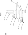
- a stimulation device 100 comprising: a probe 103 attached to a first support 101, the probe 103 comprising at least one grating coupler 121 for coupling light into the probe 103; and at least one optical source 107 for providing an optical stimulation signal mounted on a second support 102; and at least one means for detachably attaching the first support 101 to the second support 102; and wherein the position of the at least one optical source 107 is aligned with the position of the at least one grating coupler 121 to allow light emitted from the at least one optical source 107 to be received by the at least one grating coupler 121.
- the probe may be a bio-probe, a neuroprobe such as a silicon neuroprobe, or a biosensor.
- Figures 1 , 2 , 3 , 4 illustrate different views of an example embodiment:
- the first support 101 comprises the probe 123 which is attached to a first side 104 of the first support 101.
- the probe 103 is glued to the first support 101.
- the probe 103 comprises grating couplers 121 which are facing away from the first side 104 of the first support 101.
- the grating couplers 121 are used to couple light from one or more optical sources 107 into the probe 103.
- the optical sources 107 are mounted onto the second support 102.
- the optical sources 107 may be LEDs.
- the first support 101 can be attached to the second support 102 by using a means for detachably attaching the first support 101 to the second support 102.
- the means for detachably attaching the first support 101 to the second support 102 may be a nut 111 and a bolt 110.
- the first and second support 101, 102 may feature a through-hole 109, 126, 131 allowing insertion of the bolt 110 through both supports 101, 102.
- Multiple through-holes 109, 126, 131 may be present if multiple nuts 111 and bolts 110 are used to attach both supports 101, 102 to each other.
- the first support 101 can be detached from the second support 102, which allows re-use of the second support 102 while the first support 101 can be disposed of.
- this reduces costs as expensive electronic parts (e.g. optical sources 107 on the second support 102) may be reused instead of being disposed of.
- the optical sources 107 are part of the stimulation device 100 no bulky optical fibers need to be attached to the device 100 for providing optical signals which may limit the compactness of the device.
- the device 100 may be very compact.
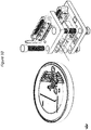
- Figure 7 illustrates the compactness of the device 100 by comparing it with a one euro coin. Also, in contrast with the use of optical fibers, no care should be taken towards the angle of the optical signal entering the device as the optical sources 107 are fixed on the second support 102.
- the position of one optical source 107 is aligned with the position of one grating coupler 121. This allows light emitted by the optical source 107 to be received by the grating coupler 121 to which it is aligned. As an advantage, a more intense optical signal may be received by the grating coupler 121.
- each optical source 107 is associated with a different grating coupler 121 on the probe 103.
- One optical sources 107 can only be associated with one grating coupler 121.
- the first and/or second supports 101, 102 are printed circuit boards.
- the use of printed circuit boards allows the addition of other electronic components on both supports 101, 102 which may be electrically interconnected using wire bonding.
- a processor or other components may be mounted on the first support 101 enabling e.g. pre-processing of data sensed by electrodes on the probe 103.
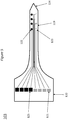
- the probe 103 further comprises: a tip 124; a shaft 119 comprising at least one electrode 122 and at least one optical stimulation site 123, the optical stimulation site 123 being optically connected to the at least one grating coupler 121; and wherein the at least one grating coupler 121 is mounted on a head 120 and wherein the head 120 is mounted on the first support 101 and wherein the head further comprises at least one bondpad 125 electrically connected to the at least one electrode 122.
- Figure 5 illustrates an embodiment of a probe 103.
- the probe 103 may be used as in-vivo device wherein the shaft 119 of the probe 103 may be inserted in the human body or brain to stimulate tissue or cells.
- the shaft 119 of the probe 103 may comprise one or more optical stimulation sites 123 which may be used to optically stimulate biological cells such as neurons.
- an optical waveguide may be embedded in the probe 103 connecting each stimulation site 123 optically to a different grating coupler 121.
- One or more grating couplers 121 are present on the head 120 of the probe 103.
- the shaft 119 of the probe 103 may comprise one or more electrodes 122 (e.g. metal electrodes) which may be used to record biological signals from cells.
- the electrodes 122 are electrically connected to bondpads 125 located on the head of the probe via a metal wire which may be embedded in the probe 103.
- the head 120 of the probe 103 is attached to the first support 101. This allows the shaft 119 to be inserted in the body or in the brain while the first support 101, the second support 102 and the head 120 remain external to the body or brain.
- the device may be used as an in-vivo device.
- the tip 124 of the probe 103 may be a sharp tip.
- the probe 103 may comprise: a silicon substrate; an interconnection layer; at least one electrode 122 electrically connected to at least one bondpad 125 via the interconnection layer; at least one optical stimulation site 123 optically connected to the at least one grating coupler 121 via the interconnection layer.
- the probe may comprise -a silicon substrate, atop the silicon substrate an interconnection layer may be present, atop the interconnection layer grating couplers, optical stimulation sites and electrodes may be present.
- the interconnection layer may comprise electrical and optical connections and may function as an interconnection between electrical components and between optical components.
- the at least one grating coupler 121 may be optically connected to the at least one optical stimulation site 123 via an optical waveguide which may be part of the interconnection layer.
- the at least one bondpad 125 may be electrically connected to the at least one electrode 122 via metal wires which may be part of the interconnection layer.
- the probe 103 may be attached (e.g.
- the probe 103 may be a micro-chip (e.g. a silicon chip). This extends the use of the device to in vitro applications. The device may be used to grow cells or place a tissue slice on the probe 103 and stimulate/record the cells or tissue slice.
- the first support 101 further comprises an electrical connector 106 located on the first support 101 and electrically connected to the at least one bondpad 125 of the probe 103.
- the electrical connector 106 may be mounted on the first support 101. If the probe 103 is a micro-chip (e.g. a biosensor), the electrical connector 106 may be at least one external bondpad 132 which may be electrically connected to at least one bondpad 125 of the micro-chip via metal wires which may be embedded in the first support 101.
- the electrical connector 106 may be used to connect an external registration device which receives, records and/or processes signals from biological cells, sensed by electrodes present on the probe 103.
- the external registration device may be a computing unit.
- the electrical connector 106 may be electrically connected to bondpads 125 of the probe 103 via bond wires.
- the bondwires may be -embedded in the first support 101.
- the electrical connector 106 is mounted on the side of the first support 101 opposite to the first side 104 of the first support 101. The location of the electrical connector 106 may be determined and changed to increase the compactness of the device 100.
- the second support 102 further comprises an optical connector 108 electrically connected to the at least one optical source 107 for powering and/or controlling the at least one optical source 107.
- the optical connector 108 may be electrically connected to the optical sources 107 via bond wires.
- the optical connector 108 may be used to power and/or to control the optical sources 107.
- the optical connector 108 may be connected to an external device suitable for generating the signals for driving and/or powering the optical sources 107, e.g. an electric signal generator.
- the optical connector 108 may be mounted on the first side 105 of the second support 102.
- the location of the optical connector 108 may be determined and changed to increase the compactness of the device 100, e.g. the optical connector 108 may be mounted on the side opposite to the first side 105 of the second support 102.
- the first or the second support 101, 102 further comprises at least one guiding means 113, 128 for aligning the position of the at least one grating coupler 121 with the position of the at least one optical source 107.
- the guiding means 113 are one or more posts which are positioned on the first or the second supports 101, 102.
- the posts may be fabricated from a sturdy material such as a metal.
- the guiding means 113 are used to ease aligning the position of the grating couplers 121 of the probe 103 with the position of the optical sources 107 of the second support 102.
- the guiding means 113 may be positioned on the second support 102 wherein the first support 101 features a corresponding through-hole 112 to allow inserting the guiding means through the through-hole 112.
- the position of the guiding means 113 are determined to automatically align the position of the optical sources 107 with the position of the grating couplers 121 when the first support 101 is attached to the second support 102.
- the guiding means 113 are inserted through their corresponding through-holes 112. Thereafter, the first support 101 may be attached to the second support 102.
- the stimulation device 100 further comprises an interface fitting 114 located in between the first support 101 and the second support 102; the interface fitting 114 comprises at least one through-hole 115 of which the position is aligned on one side of the interface fitting 114 with one of the at least one grating coupler 121 and on the other side of the interface fitting 114 with one of the at least one optical source 107.
- the through holes 115 in the interface fitting 114 confine the light emitted by optical sources 107 resulting in an aligned optical signal being received by grating couplers 121. Also, cross illumination between different optical sources is avoided. The interface fitting 114 ensures that cross-illumination between optical sources 107 is avoided. As an advantage, multiple optical sources 107 may be used. Each grating coupler 121 is allowed to receive light from one corresponding optical source 107. To avoid light from other optical sources 107 different from its corresponding optical source 107 being received by a grating coupler 121, the interface fitting 114 is placed in between the first and the second support 101, 102.
- a through-hole 115 is present in the interface fitting 114.
- the position of the through-hole 115 corresponds on one side of the interface fitting 114 with a grating coupler 121 and on the opposite side with its corresponding optical source 107.
- the interface fitting 114 may be a printed circuit board. According to another embodiment, the interface fitting 114 may be fabricated from a thermal insulating material (e.g. a thermal insulating polymer composite material). The thermal insulating material may be used to isolate the probe 103 from any heat which may be generated by optical sources 107.
- a distance equal to the thickness of the interface fitting 114 is created between the first support 101 and the second support 102. As an advantage, the distance ensures that heat which may be generated by the optical sources 107 is not transferred to the probe 103 which minimizes tissue damage in the brain caused by the heating up of the probe 103.
- the interface fitting 114 features a cut-out 116 for providing space for bond wires on the first support 101.
- the interface fitting 114 is positioned in between the first support 101 and the second support 102.
- the interface fitting 114 may feature a cut-out 116 or an opening to avoid bond wires which connect the electrical connector 106 to the probe 103 and which are present on the first side 104 of the first support 101, being covered or squeezed by the interface fitting 114. As an advantage, this allows the device to be more compact.
- the interface fitting 114 may further comprise other through-holes 130 to accommodate a means for attaching the first support 101 to the second 102 support and/or to accommodate a guiding means.
- the stimulation device 100 further comprises a gasket fitting 117 located in between the first support 101 and the second support 102; the gasket fitting 117 comprises at least one through-hole 118 of which the position is aligned on one side of the gasket fitting 117 with one of the at least one grating coupler 121 and on the other side of the gasket fitting 117 with one the at least one optical source 107.
- the gasket fitting 117 is fabricated from a flexible or elastic material.
- the gasket fitting 117 may be located in between the first support 101 and the interface fitting 114.
- light from optical sources 107 is not diffused when reaching grating couplers 121.
- the gasket fitting 117 features through-holes 118 of which the number and position correspond to the number and position of through-holes 115 of the interface fitting 114.
- the gasket fitting 117 may further comprise other through-holes 129 to accommodate a means for attaching the first 101 to the second 102 support and/or to accommodate a guiding means.
Landscapes
- Health & Medical Sciences (AREA)
- Life Sciences & Earth Sciences (AREA)
- Engineering & Computer Science (AREA)
- Biomedical Technology (AREA)
- General Health & Medical Sciences (AREA)
- Pathology (AREA)
- Animal Behavior & Ethology (AREA)
- Veterinary Medicine (AREA)
- Public Health (AREA)
- Molecular Biology (AREA)
- Neurology (AREA)
- Biophysics (AREA)
- Physics & Mathematics (AREA)
- Radiology & Medical Imaging (AREA)
- Nuclear Medicine, Radiotherapy & Molecular Imaging (AREA)
- Medical Informatics (AREA)
- Immunology (AREA)
- Heart & Thoracic Surgery (AREA)
- Surgery (AREA)
- Neurosurgery (AREA)
- Physiology (AREA)
- Chemical & Material Sciences (AREA)
- Hematology (AREA)
- Urology & Nephrology (AREA)
- Psychology (AREA)
- Cell Biology (AREA)
- Microbiology (AREA)
- Biotechnology (AREA)
- Tropical Medicine & Parasitology (AREA)
- Food Science & Technology (AREA)
- Medicinal Chemistry (AREA)
- Analytical Chemistry (AREA)
- Biochemistry (AREA)
- General Physics & Mathematics (AREA)
- Measurement Of The Respiration, Hearing Ability, Form, And Blood Characteristics Of Living Organisms (AREA)
Description
- The invention is related to devices for the stimulation of cells. In particular, the invention is related to compact and reusable neuro-stimuiation devices for the optical stimulation of biological cells such as nervous tissue. The invention is related to in-vivo and in-vitro devices for such purposes.
- Optical stimulation of neurons in the brain based on optogenetic targeting of specific neurons is the next big thing in neuroscience. The technique makes it possible to stimulate specific neurons by light of a certain wavelength. Different stimulation devices are on the market today. However, these devices have some limitations.
- A first group of state of the art stimulation devices uses probes with optical stimulation sites located on the probes, optically connected to optical fibers. These probes are inserted in the brain and the optical stimulation sites are used to stimulate particular areas of the brain. To couple light into the probe, optical fibers are attached to the probe. The use of optical fibers poses problems as they are bulky. A first problem is the compactness of the device which is reduced due to the attachment of optical fibers to a probe. The problem increases when multiple optical fibers are connected to the probe to stimulate nervous tissue with light of multiple wavelengths. A second problem is the connectivity between the probe and the optical fiber. It requires a special connection in order to couple light efficiently in the probe (e.g. the angle in which the light enters the probe needs to be correct). Thus, specific, bulky connectors are necessary which increase the size and the cost of the device.
- A second group of state of the art stimulation devices uses probes with optical sources positioned on the probes. The light of the optical source is coupled into the probes to stimulate specific regions of the brain. The problem with these devices is undesired heating, which is generated by the optical source. As the optical sources are positioned on the probes, the neurprobes tend to heat up. As a result, nervous tissue near the probe tends to heat up, resulting in tissue damage and unwanted side effects.
- A different issue which arises with current state of the art optical neural stimulation devices is the reusability factor. Current optical probes are usually used only once and cannot be reused. After stimulation, the probe is disposed.
-
US Patent Application 2011/0122366 A1 describes a single-fiber multi-spot laser probe for ophthalmic endoiliumination. The ophthalmic endoilluminator includes a light source, a first optical assembly, an optical coupling element, and an optical fiber having an optical grating located distally on the optical fiber, the optical fiber optically coupled to the optical coupling element. - There is a need for stimulation devices which can overcome at least one of the drawbacks mentioned above.
- The invention is defined by the claims. Aspects, embodiments and examples disclosed herein which do not fall within the scope of the appended claims do not form part of the invention, and are merely provided for illustrative purposes.
- In a first aspect of the invention, a neuro-stimulation device is presented according to claim 1.
- According to an example embodiment, the neuroprobe may further comprises: a tip; a shaft comprising at least one electrode and at least one optical stimulation site which is optically connected to the at least one grating coupler; and wherein the at least one grating coupler is mounted on a head which is mounted on the first support and the head further comprises at least one bondpad electrically connected to the at least one electrode. While only the head of the probe is mounted to the first support, the shaft of the probe may be inserted in the human body or brain while the rest of the device remains outside of the body. As an advantage, this allows the device to be used as an in-vivo device.
- According to an example embodiment, the neuroprobe may further comprises: a silicon substrate; an interconnection layer; at least one electrode electrically connected to at least one bondpad via the interconnection layer; at least one optical stimulation site optically connected to the at least one grating coupler via the interconnection layer. The device allows cells or tissue to be placed on top of the probe for stimulation or recording purposes. As an advantage, the device may be used as an in-vitro device.
- According to an example embodiment, the first support may further comprises an electrical connector which is electrically connected to at least one bondpad of the probe. The electrical connector allows the probe to be connected to another device for read-out of electrical signals from the probe.
- According to an example embodiment, the second support may further comprises an optical connector electrically connected to the at least one optical source for powering and/or controlling the at least one optical source. The optical connector allows connecting the at least one optical source to an external device for controlling the at least one optical source. As an advantage, the device is compact as no optical fibers need to be attached to the device.
- According to an example embodiment, the at least one means for detachably attaching the first support to the second support is a bolt and a nut.
- According to an example embodiment, the first or the second support may further comprises at least one guiding means for aligning the position of the at least one grating coupler with the position of the at least one optical source. The at least one guiding means is used to align the first support with the second support to align the position of the at least one grating coupler with the position of the at least one optical source. As an advantage, light emitted by the at least one optical source is not diffused before reaching the at least one grating coupler.
- According to an example embodiment, the device further comprises an interface fitting located in between the first support and the second support; the interface fitting comprising at least one through-hole aligned on one side of the interface fitting with one of the at least one grating coupler and on the other side of the interface fitting with one of the at least one optical source . The interface fitting is used to align grating couplers with optical sources on a one-to-one basis to avoid cross-illumination between optical sources. As an advantage, multiple optical sources may be used.
- According to an example embodiment, the interface fitting features a cut-out for providing space for bond wires on the first support. The cut-out provides space e.g. for bond wires which may present on the first support. As an advantage, the first support may be attached to the second support in a very compact manner.
- According to an example embodiment, the device further comprises a gasket fitting located in between the first support and the second support; the gasket fitting comprising at least one through-hole aligned on one side of the gasket fitting with one of the at least one grating coupler and on the other side of the gasket fitting with one of the at least one optical source. The gasket fitting ensures a perfect fitting between the interface fitting and the second support.
- According to an example embodiment, the neuroprobe is glued to the first support.
- According to an example embodiment, the first support and/or the second support and/or the interface fitting are printed circuit boards.
- According to an example embodiment, the gasket fitting is fabricated from an elastic material. Due to the elastic material the gasket fitting is flexible. As an advantage, a perfect and tight fitting between the interface fitting and the second support is possible.
- According to an example embodiment, the at least one optical source is a LED.
- The neuron-stimulation device may be used as a bio-probe, a neuroprobe or a biosensor.
- The neuron-stimulation device may be used for the stimulation of biological cells such as neurons in the brain, biological cells in the body.
-
-
Figure 1 illustrates a 2D side view of a de-assembled embodiment using a neuroprobe -
Figure 2 illustrates a 2D backside view of a de-assembled embodiment using a neuroprobe -
Figure 3 illustrates a 3D frontside view of an embodiment using a neuroprobe -
Figure 4 illustrates a 3D frontside view of an embodiment using a neuroprobe -
Figure 5 illustrates an embodiment of a probe -
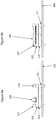
Figure 6 illustrates a 3D frontside view of an embodiment using a micro-chip -
Figure 7 illustrates a 3D frontside view of a de-assembled embodiment using a micro-chip -
Figure 8a illustrates a 2D backside view -of a de-assembled embodiment using a micro-chip -
Figure 8b illustrates a 2D frontside view -of a de-assembled embodiment using a micro-chip -
Figure 9a illustrates a 2D backside view -of an assembled embodiment using a micro-chip -
Figure 9b illustrates a 2D frontside view -of an assembled embodiment using a micro-chip -
Figure 10 illustrates the compactness of the device - Where in embodiments of the present disclosure reference is made to "a PCB", this is defined as a printed circuit board. A printed circuit board is used to mechanically support and electrically connect electronic components using conductive pathways, tracks or signal traces etched from e.g. copper sheets laminated onto a non-conductive substrate.
- Where in embodiments of the present disclosure reference is made to "a bondpad", this is defined as an electrically conductive, e.g. metallized, area on a surface of a semiconductor device to which connections can be made.
- Where in embodiments of the present disclosure reference is made to "wire bonding", this is defined as a technique for making interconnections between an integrated circuit (IC) and a printed circuit board (PCB) during semiconductor device fabrication. The interconnection itself can be defined as "a bond wire". Wire bonding can also be used to make an electrical connection between two nodes on a PCB.
- Where in embodiments of the present disclosure reference is made to "a probe", this is defined as a device to stimulate biological cells.
- Where in embodiments of the present disclosure reference is made to "a bio-probe", this is defined as a probe which may be inserted in the body for the stimulation of e.g. organ tissue. Such a bio-probe may be used e.g. to relieve pain. The bio-probe may be an electrical or an optical stimulation device or a combination thereof.
- Where in embodiments of the present disclosure reference is made to "a neuroprobe", this is defined as a probe which may be inserted in the brain for the stimulation of nervous tissue. Such a neuroprobe may be also used to record data from neurons in the brain. The neuroprobe may be an electrical or an optical stimulation device or a combination thereof.
- Where in embodiments of the present disclosure reference is made to "a post", this is defined as a piece fixed firmly in an upright position which may be used as a stay or support.
- The device presented in this disclosure may be used to optically stimulate biological cells. The device may be used to stimulate nervous tissue in the brain or cells in the body. The device may also be used to record electrochemical activity from biological cells such as neurons in the brain after or during optical stimulation.
- In a first example, a
stimulation device 100 is presented comprising: aprobe 103 attached to afirst support 101, theprobe 103 comprising at least onegrating coupler 121 for coupling light into theprobe 103; and at least oneoptical source 107 for providing an optical stimulation signal mounted on asecond support 102; and at least one means for detachably attaching thefirst support 101 to thesecond support 102; and wherein the position of the at least oneoptical source 107 is aligned with the position of the at least onegrating coupler 121 to allow light emitted from the at least oneoptical source 107 to be received by the at least onegrating coupler 121. - According to an example embodiment invention, the probe may be a bio-probe, a neuroprobe such as a silicon neuroprobe, or a biosensor.
-
Figures 1 ,2 ,3 ,4 illustrate different views of an example embodiment: -
Figure 1 illustrates a side-view of an embodiment of ade-assembled stimulation device 100. Illustrated are: anelectrical connector 106 and aprobe 103 located on anfirst support 101; anoptical connector 108 andoptical sources 107 located on ansecond support 102; aninterface fitting 114; a gasket fitting 117; abolt 110; anut 111 and a guidingpost 113. -
Figure 2 illustrates a backside view of an embodiment of ade-assembled stimulation device 100. Illustrated are: anelectrical connector 106 and aprobe 103 withgrating couplers 121 located on anfirst support 101; anoptical connector 108 located on ansecond support 102; aninterface fitting 114 with cut-out 116; a gasket fitting 117; anut 111; abolt 110 and a guidingpost 113. -
Figure 3 illustrates a 3D view of the backside of a de--assembledstimulation device 100. Illustrated are: anelectrical connector 106 and aprobe 103 located on anfirst support 101 with through-holes 109; anoptical connector 108 located on ansecond support 102 with a trough-hole 126 suitable for receiving abolt 110; aninterface fitting 114 with a cut-out 116; a gasket fitting 117; twobolts posts -
Figure 4 illustrates a 3D view of the frontside of a de--assembledstimulation device 100. Illustrated are: twobolts posts electrical connector 106 and aprobe 103 located on anfirst support 101 with through-holes 109; anoptical connector 108 andoptical sources 107 located on ansecond support 102 with throughholes holes interface fitting 114 with throughholes - The
first support 101 comprises theprobe 123 which is attached to afirst side 104 of thefirst support 101. According to an embodiment, theprobe 103 is glued to thefirst support 101. Theprobe 103 comprisesgrating couplers 121 which are facing away from thefirst side 104 of thefirst support 101. Thegrating couplers 121 are used to couple light from one or moreoptical sources 107 into theprobe 103. Theoptical sources 107 are mounted onto thesecond support 102. According to an embodiment, theoptical sources 107 may be LEDs. Thefirst support 101 can be attached to thesecond support 102 by using a means for detachably attaching thefirst support 101 to thesecond support 102. According to an embodiment, the means for detachably attaching thefirst support 101 to thesecond support 102 may be anut 111 and abolt 110. When anut 111 and abolt 110 are used, the first andsecond support hole bolt 110 through bothsupports holes multiple nuts 111 andbolts 110 are used to attach bothsupports - The
first support 101 can be detached from thesecond support 102, which allows re-use of thesecond support 102 while thefirst support 101 can be disposed of. As an advantage, this reduces costs as expensive electronic parts (e.g.optical sources 107 on the second support 102) may be reused instead of being disposed of. This in contrast with state of the art devices which cannot be de-assembled and therefore their reusability is limited. As theoptical sources 107 are part of thestimulation device 100 no bulky optical fibers need to be attached to thedevice 100 for providing optical signals which may limit the compactness of the device. As an advantage, thedevice 100 may be very compact.Figure 7 illustrates the compactness of thedevice 100 by comparing it with a one euro coin. Also, in contrast with the use of optical fibers, no care should be taken towards the angle of the optical signal entering the device as theoptical sources 107 are fixed on thesecond support 102. - When the
first support 101 is attached to thesecond support 102, the position of oneoptical source 107 is aligned with the position of onegrating coupler 121. This allows light emitted by theoptical source 107 to be received by thegrating coupler 121 to which it is aligned. As an advantage, a more intense optical signal may be received by thegrating coupler 121. When multipleoptical sources 107 are present on thesecond support 102, eachoptical source 107 is associated with a differentgrating coupler 121 on theprobe 103. Oneoptical sources 107 can only be associated with one gratingcoupler 121. - According to an embodiment, the first and/or
second supports supports first support 101 enabling e.g. pre-processing of data sensed by electrodes on theprobe 103. - According to an embodiment, the
probe 103 further comprises: atip 124; ashaft 119 comprising at least oneelectrode 122 and at least oneoptical stimulation site 123, theoptical stimulation site 123 being optically connected to the at least onegrating coupler 121; and wherein the at least onegrating coupler 121 is mounted on ahead 120 and wherein thehead 120 is mounted on thefirst support 101 and wherein the head further comprises at least onebondpad 125 electrically connected to the at least oneelectrode 122.Figure 5 illustrates an embodiment of aprobe 103. - The
probe 103 may be used as in-vivo device wherein theshaft 119 of theprobe 103 may be inserted in the human body or brain to stimulate tissue or cells. - The
shaft 119 of theprobe 103 may comprise one or moreoptical stimulation sites 123 which may be used to optically stimulate biological cells such as neurons. According to an embodiment, an optical waveguide may be embedded in theprobe 103 connecting eachstimulation site 123 optically to a differentgrating coupler 121. One or moregrating couplers 121 are present on thehead 120 of theprobe 103. Additionally, theshaft 119 of theprobe 103 may comprise one or more electrodes 122 (e.g. metal electrodes) which may be used to record biological signals from cells. Theelectrodes 122 are electrically connected to bondpads 125 located on the head of the probe via a metal wire which may be embedded in theprobe 103. - The
head 120 of theprobe 103 is attached to thefirst support 101. This allows theshaft 119 to be inserted in the body or in the brain while thefirst support 101, thesecond support 102 and thehead 120 remain external to the body or brain. As an advantage, the device may be used as an in-vivo device. To ease insertion, thetip 124 of theprobe 103 may be a sharp tip. - According to an embodiment, the
probe 103 may comprise: a silicon substrate; an interconnection layer; at least oneelectrode 122 electrically connected to at least onebondpad 125 via the interconnection layer; at least oneoptical stimulation site 123 optically connected to the at least onegrating coupler 121 via the interconnection layer. - The probe may comprise -a silicon substrate, atop the silicon substrate an interconnection layer may be present, atop the interconnection layer grating couplers, optical stimulation sites and electrodes may be present. The interconnection layer may comprise electrical and optical connections and may function as an interconnection between electrical components and between optical components. The at least one
grating coupler 121 may be optically connected to the at least oneoptical stimulation site 123 via an optical waveguide which may be part of the interconnection layer. The at least onebondpad 125 may be electrically connected to the at least oneelectrode 122 via metal wires which may be part of the interconnection layer. Theprobe 103 may be attached (e.g. glued) to thefirst support 101 such that the at least oneelectrode 122, the at least onegrating coupler 121 and the at least oneoptical stimulation site 123 are facing away from thefirst support 101 to allow recording and stimulation of biological cells or slices of biological tissue placed or grown on the silicon chip. Such an embodiment is illustrated inFigures 6 ,7 ,8a, 8b ,9a and 9b . Theprobe 103 may be a micro-chip (e.g. a silicon chip). This extends the use of the device to in vitro applications. The device may be used to grow cells or place a tissue slice on theprobe 103 and stimulate/record the cells or tissue slice. - According to an embodiment, the
first support 101 further comprises anelectrical connector 106 located on thefirst support 101 and electrically connected to the at least onebondpad 125 of theprobe 103. Theelectrical connector 106 may be mounted on thefirst support 101. If theprobe 103 is a micro-chip (e.g. a biosensor), theelectrical connector 106 may be at least oneexternal bondpad 132 which may be electrically connected to at least onebondpad 125 of the micro-chip via metal wires which may be embedded in thefirst support 101. - The
electrical connector 106 may be used to connect an external registration device which receives, records and/or processes signals from biological cells, sensed by electrodes present on theprobe 103. The external registration device may be a computing unit. Theelectrical connector 106 may be electrically connected to bondpads 125 of theprobe 103 via bond wires. The bondwires may be -embedded in thefirst support 101. According to an embodiment, theelectrical connector 106 is mounted on the side of thefirst support 101 opposite to thefirst side 104 of thefirst support 101. The location of theelectrical connector 106 may be determined and changed to increase the compactness of thedevice 100. - According to an embodiment, the
second support 102 further comprises anoptical connector 108 electrically connected to the at least oneoptical source 107 for powering and/or controlling the at least oneoptical source 107. - The
optical connector 108 may be electrically connected to theoptical sources 107 via bond wires. Theoptical connector 108 may be used to power and/or to control theoptical sources 107. Theoptical connector 108 may be connected to an external device suitable for generating the signals for driving and/or powering theoptical sources 107, e.g. an electric signal generator. According to an embodiment, theoptical connector 108 may be mounted on thefirst side 105 of thesecond support 102. The location of theoptical connector 108 may be determined and changed to increase the compactness of thedevice 100, e.g. theoptical connector 108 may be mounted on the side opposite to thefirst side 105 of thesecond support 102. - According to an embodiment, the first or the
second support grating coupler 121 with the position of the at least oneoptical source 107. - According to an embodiment, the guiding means 113 are one or more posts which are positioned on the first or the
second supports grating couplers 121 of theprobe 103 with the position of theoptical sources 107 of thesecond support 102. The guiding means 113 may be positioned on thesecond support 102 wherein thefirst support 101 features a corresponding through-hole 112 to allow inserting the guiding means through the through-hole 112. When guiding means 113 are used, the position of the guiding means 113 are determined to automatically align the position of theoptical sources 107 with the position of thegrating couplers 121 when thefirst support 101 is attached to thesecond support 102. Before attaching thefirst support 101 to thesecond support 102, the guiding means 113 are inserted through their corresponding through-holes 112. Thereafter, thefirst support 101 may be attached to thesecond support 102. - According to an embodiment, the
stimulation device 100 further comprises aninterface fitting 114 located in between thefirst support 101 and thesecond support 102; the interface fitting 114 comprises at least one through-hole 115 of which the position is aligned on one side of the interface fitting 114 with one of the at least onegrating coupler 121 and on the other side of the interface fitting 114 with one of the at least oneoptical source 107. - The through
holes 115 in the interface fitting 114 confine the light emitted byoptical sources 107 resulting in an aligned optical signal being received by gratingcouplers 121. Also, cross illumination between different optical sources is avoided. Theinterface fitting 114 ensures that cross-illumination betweenoptical sources 107 is avoided. As an advantage, multipleoptical sources 107 may be used. Eachgrating coupler 121 is allowed to receive light from one correspondingoptical source 107. To avoid light from otheroptical sources 107 different from its correspondingoptical source 107 being received by agrating coupler 121, the interface fitting 114 is placed in between the first and thesecond support optical source 107 and its correspondinggrating coupler 121, a through-hole 115 is present in theinterface fitting 114. The position of the through-hole 115 corresponds on one side of the interface fitting 114 with agrating coupler 121 and on the opposite side with its correspondingoptical source 107. - According to an embodiment, the interface fitting 114 may be a printed circuit board. According to another embodiment, the interface fitting 114 may be fabricated from a thermal insulating material (e.g. a thermal insulating polymer composite material). The thermal insulating material may be used to isolate the
probe 103 from any heat which may be generated byoptical sources 107. By using the interface fitting 114, a distance equal to the thickness of the interface fitting 114 is created between thefirst support 101 and thesecond support 102. As an advantage, the distance ensures that heat which may be generated by theoptical sources 107 is not transferred to theprobe 103 which minimizes tissue damage in the brain caused by the heating up of theprobe 103. - According to an embodiment, the interface fitting 114 features a cut-out 116 for providing space for bond wires on the
first support 101. - The
interface fitting 114 is positioned in between thefirst support 101 and thesecond support 102. Theinterface fitting 114 may feature a cut-out 116 or an opening to avoid bond wires which connect theelectrical connector 106 to theprobe 103 and which are present on thefirst side 104 of thefirst support 101, being covered or squeezed by theinterface fitting 114. As an advantage, this allows the device to be more compact. Theinterface fitting 114 may further comprise other through-holes 130 to accommodate a means for attaching thefirst support 101 to the second 102 support and/or to accommodate a guiding means. - According to an embodiment, the
stimulation device 100 further comprises a gasket fitting 117 located in between thefirst support 101 and thesecond support 102; the gasket fitting 117 comprises at least one through-hole 118 of which the position is aligned on one side of the gasket fitting 117 with one of the at least onegrating coupler 121 and on the other side of the gasket fitting 117 with one the at least oneoptical source 107. - According to an embodiment, the gasket fitting 117 is fabricated from a flexible or elastic material. The gasket fitting 117 may be located in between the
first support 101 and theinterface fitting 114. As the gasket fitting 117 is flexible, it ensures a good and tight fitting between theinterface fitting 114 and thefirst support 101 when thefirst support 101 is attached to thesecond support 102. As an advantage, light fromoptical sources 107 is not diffused when reachinggrating couplers 121. The gasket fitting 117 features through-holes 118 of which the number and position correspond to the number and position of through-holes 115 of theinterface fitting 114. The gasket fitting 117 may further comprise other through-holes 129 to accommodate a means for attaching the first 101 to the second 102 support and/or to accommodate a guiding means.
Claims (14)
- A neuro-stimulation device (100) comprising:- a neuroprobe (103) attached to a first support (101), the neuroprobe (103) comprising a plurality of grating couplers (121) for coupling light into the neuroprobe (103); and- a plurality of optical sources (107) for providing an optical stimulation signal, mounted on a second support (102); and- at least one means for detachably attaching the first support (101) to the second support (102); andwherein the position of each optical source (107) is aligned with the position of a different grating coupler (121) to allow light emitted from each optical source (107) to be received by a grating coupler (121) ; and
wherein the neuroprobe (103) comprises a plurality of optical stimulation sites (123), each optical stimulation site (123) being optically connected to a different grating coupler (121). - The neuron-stimulation device (100) according to claim 1 wherein the neuroprobe (103) further comprises:- a tip (124);- a shaft (119) comprising at least one electrode (122) and the plurality of optical stimulation sites (123); and- wherein the plurality of grating couplers (121) are mounted on a head (120) which is mounted on the first support (101) and the head further comprises at least one bondpad (125) electrically connected to the at least one electrode (122).
- The neuron-stimulation device (100) according to claim 1 wherein the probe (103) further comprises:- a silicon substrate;- an interconnection layer;- at least one electrode (122) electrically connected to at least one bondpad (125) via the interconnection layer;- wherein each optical stimulation site (123) is optically connected to a different grating coupler (121) via the interconnection layer.
- A neuron-stimulation device (100) according to any of the preceding claims, wherein the first support (101) further comprises an electrical connector (106) which is electrically connected to the at least one bondpad (125) of the neuroprobe (103).
- A neuron-stimulation device (100) according to any of the preceding claims, wherein the second support (102) further comprises an optical connector (108) electrically connected to the plurality of optical sources (107) for powering and/or controlling the plurality of optical sources (107).
- The neuron-stimulation device (100) according to any of the preceding claims, wherein the at least one means for detachably attaching the first support (101) to the second support (102) is a bolt (110) and a nut (111).
- The neuron-stimulation device (100) according to any of the preceding claims, wherein the first or the second support (101, 102) further comprises at least one guiding means (113) for aligning the position of the plurality of grating couplers (121) with the position of the plurality of optical sources (107).
- The neuron-stimulation device (100) according to any of the preceding claims, further comprising an interface fitting (114) located in between the first support (101) and the second support (102); the interface fitting (114) comprising a plurality of through-holes (115), each through-hole (115) aligned on one side of the interface fitting (114) with one of the plurality of grating couplers (121) and on the other side of the interface fitting (114) with one of the plurality of optical sources (107) .
- The neuron-stimulation device (100) according to claim 8 wherein the interface fitting (114) features a cut-out (116) for providing space for bond wires on the first support (101).
- The neuron-stimulation device (100) according to any of the preceding claims, further comprising an gasket fitting (117) located in between the first support (101) and the second support (102); the gasket fitting (117) comprising a plurality of through-holes (118), each through-hole (118) aligned on one side of the gasket fitting (117) with one of the plurality of grating couplers (121) and on the other side of the gasket fitting (117) with one of the plurality of optical sources (107).
- The neuron-stimulation device (100) according to any of the preceding claims wherein the neuroprobe (103) is glued to the first support (101).
- The neuron-stimulation device (100) according to any of the preceding claims wherein the first support (101) and/or the second support (102) and/or the interface fitting (114) are printed circuit boards.
- The neuron-stimulation device (100) according to any of the preceding claims wherein the gasket fitting (117) is fabricated from an elastic material.
- The neuron-stimulation device (100) according to any of the preceding claims wherein the plurality of optical sources (107) are LEDs.
Priority Applications (2)
| Application Number | Priority Date | Filing Date | Title |
|---|---|---|---|
| EP13169700.5A EP2808056B1 (en) | 2013-05-29 | 2013-05-29 | Optical stimulation device |
| US14/289,876 US10159419B2 (en) | 2013-05-29 | 2014-05-29 | Optical stimulation device |
Applications Claiming Priority (1)
| Application Number | Priority Date | Filing Date | Title |
|---|---|---|---|
| EP13169700.5A EP2808056B1 (en) | 2013-05-29 | 2013-05-29 | Optical stimulation device |
Publications (2)
| Publication Number | Publication Date |
|---|---|
| EP2808056A1 EP2808056A1 (en) | 2014-12-03 |
| EP2808056B1 true EP2808056B1 (en) | 2020-04-15 |
Family
ID=48537823
Family Applications (1)
| Application Number | Title | Priority Date | Filing Date |
|---|---|---|---|
| EP13169700.5A Active EP2808056B1 (en) | 2013-05-29 | 2013-05-29 | Optical stimulation device |
Country Status (2)
| Country | Link |
|---|---|
| US (1) | US10159419B2 (en) |
| EP (1) | EP2808056B1 (en) |
Families Citing this family (1)
| Publication number | Priority date | Publication date | Assignee | Title |
|---|---|---|---|---|
| US10722729B2 (en) | 2017-01-11 | 2020-07-28 | International Business Machines Corporation | Probe for localized neural optogenetics stimulation and neurochemistry recordings |
Family Cites Families (50)
| Publication number | Priority date | Publication date | Assignee | Title |
|---|---|---|---|---|
| US5135590A (en) * | 1991-05-24 | 1992-08-04 | At&T Bell Laboratories | Optical fiber alignment method |
| US5337391A (en) * | 1993-05-03 | 1994-08-09 | Motorola, Inc. | Optoelectronic sub-module and method of making same |
| JP2000516719A (en) * | 1996-08-16 | 2000-12-12 | ツェプトゼンス アクチエンゲゼルシャフト | Photodetector |
| US8688188B2 (en) * | 1998-04-30 | 2014-04-01 | Abbott Diabetes Care Inc. | Analyte monitoring device and methods of use |
| US9066695B2 (en) * | 1998-04-30 | 2015-06-30 | Abbott Diabetes Care Inc. | Analyte monitoring device and methods of use |
| US6175752B1 (en) * | 1998-04-30 | 2001-01-16 | Therasense, Inc. | Analyte monitoring device and methods of use |
| US8465425B2 (en) * | 1998-04-30 | 2013-06-18 | Abbott Diabetes Care Inc. | Analyte monitoring device and methods of use |
| US7555333B2 (en) * | 2000-06-19 | 2009-06-30 | University Of Washington | Integrated optical scanning image acquisition and display |
| US7146221B2 (en) * | 2001-11-16 | 2006-12-05 | The Regents Of The University Of California | Flexible electrode array for artifical vision |
| US20060293727A1 (en) * | 2002-05-09 | 2006-12-28 | Greg Spooner | System and method for treating exposed tissue with light emitting diodes |
| US20030233138A1 (en) * | 2002-06-12 | 2003-12-18 | Altus Medical, Inc. | Concentration of divergent light from light emitting diodes into therapeutic light energy |
| WO2004067162A2 (en) * | 2003-01-30 | 2004-08-12 | Ciphergen Biosystems Inc. | Apparatus for microfluidic processing and reading of biochip arrays |
| US7338836B2 (en) * | 2003-11-05 | 2008-03-04 | California Institute Of Technology | Method for integrating pre-fabricated chip structures into functional electronic systems |
| TWI268787B (en) * | 2004-12-30 | 2006-12-21 | Ind Tech Res Inst | Light therapeutic device |
| EP1853190A4 (en) * | 2005-03-02 | 2008-08-13 | Meridian Co Ltd | Adipose resolve apparatus for low-power laser |
| US20060217787A1 (en) * | 2005-03-23 | 2006-09-28 | Eastman Kodak Company | Light therapy device |
| US8744570B2 (en) * | 2009-01-23 | 2014-06-03 | Lockheed Martin Corporation | Optical stimulation of the brainstem and/or midbrain, including auditory areas |
| US8792978B2 (en) * | 2010-05-28 | 2014-07-29 | Lockheed Martin Corporation | Laser-based nerve stimulators for, E.G., hearing restoration in cochlear prostheses and method |
| US8012189B1 (en) * | 2007-01-11 | 2011-09-06 | Lockheed Martin Corporation | Method and vestibular implant using optical stimulation of nerves |
| US8498699B2 (en) * | 2008-10-03 | 2013-07-30 | Lockheed Martin Company | Method and nerve stimulator using simultaneous electrical and optical signals |
| US8160696B2 (en) * | 2008-10-03 | 2012-04-17 | Lockheed Martin Corporation | Nerve stimulator and method using simultaneous electrical and optical signals |
| US20080131834A1 (en) * | 2006-12-04 | 2008-06-05 | Techlight Systems Llc | Photocatalysis process toothbrush |
| US8523925B2 (en) * | 2007-01-17 | 2013-09-03 | Lerner Medical Devices, Inc. | Fiber optic phototherapy device |
| US8523926B2 (en) * | 2007-01-19 | 2013-09-03 | Joseph Neev | Devices and methods for generation of subsurface microdisruptions for biomedical applications |
| US8731673B2 (en) * | 2007-02-26 | 2014-05-20 | Sapiens Steering Brain Stimulation B.V. | Neural interface system |
| EP1985579B1 (en) * | 2007-04-27 | 2018-01-10 | IMEC vzw | Connecting scheme for the orthogonal assembly of microstructures |
| US20120123508A1 (en) * | 2010-11-12 | 2012-05-17 | Massachusetts Institute Of Technology | Methods and apparatus for wireless control of biological tissue |
| US20080306576A1 (en) * | 2007-05-09 | 2008-12-11 | Massachusetts Institute Of Technology | Optical Cell Control Prosthetics |
| US8910638B2 (en) * | 2007-05-09 | 2014-12-16 | Massachusetts Institute Of Technology | Methods and apparatus for high-throughput neural screening |
| US7566173B2 (en) * | 2007-07-09 | 2009-07-28 | Alcon, Inc. | Multi-spot ophthalmic laser probe |
| US9011508B2 (en) * | 2007-11-30 | 2015-04-21 | Lockheed Martin Corporation | Broad wavelength profile to homogenize the absorption profile in optical stimulation of nerves |
| US9289142B2 (en) * | 2008-03-24 | 2016-03-22 | Neuronexus Technologies, Inc. | Implantable electrode lead system with a three dimensional arrangement and method of making the same |
| US8168939B2 (en) * | 2008-07-09 | 2012-05-01 | Luxtera, Inc. | Method and system for a light source assembly supporting direct coupling to an integrated circuit |
| DE102009025407B4 (en) * | 2009-06-18 | 2020-07-09 | Forschungszentrum Jülich GmbH | Device for stimulating neuronal tissue using optical stimuli |
| WO2010151636A2 (en) * | 2009-06-24 | 2010-12-29 | SoundBeam LLC | Optical cochlear stimulation devices and methods |
| US8263986B2 (en) * | 2009-07-02 | 2012-09-11 | The Royal Institution For The Advancement Of Learning/Mcgill University | Optically interrogated solid state biosensors incorporating porous materials—devices |
| US8870857B2 (en) * | 2009-11-05 | 2014-10-28 | Greatbatch Ltd. | Waveguide neural interface device |
| US20130046148A1 (en) * | 2009-11-09 | 2013-02-21 | Prashant Tathireddy | Three Dimensional Penetrating Optical-Electrical Neural Interface for Selective Stimulation and Recording |
| CA2779511C (en) * | 2009-11-24 | 2018-01-02 | Alcon Research Ltd. | Single-fiber multi-spot laser probe for ophthalmic endoillumination |
| KR101296833B1 (en) * | 2009-12-08 | 2013-08-14 | 한국전자통신연구원 | Silicon Photonics Chip |
| US20110224554A1 (en) * | 2010-03-12 | 2011-09-15 | Optomak Inc. | Optogenetic Fiber Optic Cannula and Adapted Fiber Optic Connector |
| US8469610B2 (en) * | 2011-01-18 | 2013-06-25 | Avago Technologies General Ip (Singapore) Pte. Ltd. | Optical connection system with plug having optical turn |
| US9192314B2 (en) * | 2011-03-29 | 2015-11-24 | The Charles Stark Draper Laboratory, Inc. | Probe for neural recording and optical spectroscopic interrogation |
| US9801559B2 (en) * | 2011-07-25 | 2017-10-31 | Diagnostic Biochips, Inc. | Integrated optical neural probe |
| US9248269B2 (en) * | 2011-07-25 | 2016-02-02 | Neuronexus Technologies, Inc. | Neural device with modular electrode array |
| WO2013016391A1 (en) * | 2011-07-25 | 2013-01-31 | Neuronexus Technologies, Inc. | Neuromodulation transfection system with means for active fluid delivery and a method for its use |
| US20130085398A1 (en) * | 2011-09-26 | 2013-04-04 | California Institute Of Technology | Brain-machine interface based on photonic neural probe arrays |
| US9285554B2 (en) * | 2012-02-10 | 2016-03-15 | International Business Machines Corporation | Through-substrate optical coupling to photonics chips |
| US9486641B2 (en) * | 2013-03-16 | 2016-11-08 | Lawrence Livermore National Security, Llc | Incorporating an optical waveguide into a neural interface |
| US10695581B2 (en) * | 2015-06-19 | 2020-06-30 | The Regents Of The University Of Michigan | Multicolor neural optoelectrode |
-
2013
- 2013-05-29 EP EP13169700.5A patent/EP2808056B1/en active Active
-
2014
- 2014-05-29 US US14/289,876 patent/US10159419B2/en active Active
Non-Patent Citations (1)
| Title |
|---|
| None * |
Also Published As
| Publication number | Publication date |
|---|---|
| EP2808056A1 (en) | 2014-12-03 |
| US10159419B2 (en) | 2018-12-25 |
| US20140356892A1 (en) | 2014-12-04 |
Similar Documents
| Publication | Publication Date | Title |
|---|---|---|
| US7706853B2 (en) | Near infrared spectroscopy device with reusable portion | |
| US9662494B2 (en) | Probe, especially a probe for neural applications | |
| US6661161B1 (en) | Piezoelectric biological sound monitor with printed circuit board | |
| CN110785205B (en) | Implantable electrode coupled to an optoelectronic device | |
| Alt et al. | Let there be light—optoprobes for neural implants | |
| JP6464321B2 (en) | Electronic circuit unit, imaging unit and endoscope | |
| Schwaerzle et al. | Compact silicon-based optrode with integrated laser diode chips, SU-8 waveguides and platinum electrodes for optogenetic applications | |
| US20180169431A1 (en) | Flexible LED Light Pad For Phototherapy | |
| EP2947486A1 (en) | Optical transmission module and imaging device | |
| Schwaerzle et al. | Ultracompact optrode with integrated laser diode chips and SU-8 waveguides for optogenetic applications | |
| US10335603B2 (en) | Medical devices including flexible circuit bodies with exposed portions of circuit traces attached to electrical contacts of components | |
| Schwaerzle et al. | Miniaturized 3× 3 optical fiber array for optogenetics with integrated 460 nm light sources and flexible electrical interconnection | |
| Ji et al. | Flexible Optoelectric Neural Interface Integrated Wire-Bonding $\mu $ LEDs and Microelectrocorticography for Optogenetics | |
| EP2808056B1 (en) | Optical stimulation device | |
| CN101837167A (en) | Phototherapy device | |
| US11444056B2 (en) | Sandwich assembly scheme for thin film electrode array and integrated circuits on both sides of printed circuit board (PCB) and method of manufacture | |
| Park et al. | The first neural probe integrated with light source (blue laser diode) for optical stimulation and electrical recording | |
| US11986351B2 (en) | Flexible electric circuit for ultrasound catheters and related devices and methods | |
| US12023507B2 (en) | Systems and methods for flexible, high-density opto-electronic arrays | |
| EP1434209A3 (en) | Laser diode module with integrated drive chip and optical pickup apparatus adopting the same |
Legal Events
| Date | Code | Title | Description |
|---|---|---|---|
| PUAI | Public reference made under article 153(3) epc to a published international application that has entered the european phase |
Free format text: ORIGINAL CODE: 0009012 |
|
| 17P | Request for examination filed |
Effective date: 20130529 |
|
| AK | Designated contracting states |
Kind code of ref document: A1 Designated state(s): AL AT BE BG CH CY CZ DE DK EE ES FI FR GB GR HR HU IE IS IT LI LT LU LV MC MK MT NL NO PL PT RO RS SE SI SK SM TR |
|
| AX | Request for extension of the european patent |
Extension state: BA ME |
|
| R17P | Request for examination filed (corrected) |
Effective date: 20150602 |
|
| RBV | Designated contracting states (corrected) |
Designated state(s): AL AT BE BG CH CY CZ DE DK EE ES FI FR GB GR HR HU IE IS IT LI LT LU LV MC MK MT NL NO PL PT RO RS SE SI SK SM TR |
|
| RAP1 | Party data changed (applicant data changed or rights of an application transferred) |
Owner name: IMEC VZW Owner name: KATHOLIEKE UNIVERSITEIT LEUVEN |
|
| STAA | Information on the status of an ep patent application or granted ep patent |
Free format text: STATUS: EXAMINATION IS IN PROGRESS |
|
| 17Q | First examination report despatched |
Effective date: 20190103 |
|
| RIC1 | Information provided on ipc code assigned before grant |
Ipc: A61B 5/00 20060101ALI20190911BHEP Ipc: A61B 5/04 20060101ALI20190911BHEP Ipc: A61N 5/06 20060101AFI20190911BHEP |
|
| GRAP | Despatch of communication of intention to grant a patent |
Free format text: ORIGINAL CODE: EPIDOSNIGR1 |
|
| STAA | Information on the status of an ep patent application or granted ep patent |
Free format text: STATUS: GRANT OF PATENT IS INTENDED |
|
| INTG | Intention to grant announced |
Effective date: 20191105 |
|
| RAP1 | Party data changed (applicant data changed or rights of an application transferred) |
Owner name: IMEC VZW Owner name: KATHOLIEKE UNIVERSITEIT LEUVEN |
|
| RIN1 | Information on inventor provided before grant (corrected) |
Inventor name: MUSA, SILKE Inventor name: HOFFMAN, LUIS DIEGO LEON Inventor name: BRAEKEN, DRIES |
|
| GRAS | Grant fee paid |
Free format text: ORIGINAL CODE: EPIDOSNIGR3 |
|
| GRAA | (expected) grant |
Free format text: ORIGINAL CODE: 0009210 |
|
| STAA | Information on the status of an ep patent application or granted ep patent |
Free format text: STATUS: THE PATENT HAS BEEN GRANTED |
|
| AK | Designated contracting states |
Kind code of ref document: B1 Designated state(s): AL AT BE BG CH CY CZ DE DK EE ES FI FR GB GR HR HU IE IS IT LI LT LU LV MC MK MT NL NO PL PT RO RS SE SI SK SM TR |
|
| REG | Reference to a national code |
Ref country code: CH Ref legal event code: EP Ref country code: GB Ref legal event code: FG4D |
|
| REG | Reference to a national code |
Ref country code: DE Ref legal event code: R096 Ref document number: 602013067866 Country of ref document: DE |
|
| REG | Reference to a national code |
Ref country code: IE Ref legal event code: FG4D |
|
| REG | Reference to a national code |
Ref country code: AT Ref legal event code: REF Ref document number: 1256549 Country of ref document: AT Kind code of ref document: T Effective date: 20200515 |
|
| PGFP | Annual fee paid to national office [announced via postgrant information from national office to epo] |
Ref country code: GB Payment date: 20200525 Year of fee payment: 8 |
|
| REG | Reference to a national code |
Ref country code: NL Ref legal event code: MP Effective date: 20200415 |
|
| REG | Reference to a national code |
Ref country code: LT Ref legal event code: MG4D |
|
| PG25 | Lapsed in a contracting state [announced via postgrant information from national office to epo] |
Ref country code: NO Free format text: LAPSE BECAUSE OF FAILURE TO SUBMIT A TRANSLATION OF THE DESCRIPTION OR TO PAY THE FEE WITHIN THE PRESCRIBED TIME-LIMIT Effective date: 20200715 Ref country code: GR Free format text: LAPSE BECAUSE OF FAILURE TO SUBMIT A TRANSLATION OF THE DESCRIPTION OR TO PAY THE FEE WITHIN THE PRESCRIBED TIME-LIMIT Effective date: 20200716 Ref country code: IS Free format text: LAPSE BECAUSE OF FAILURE TO SUBMIT A TRANSLATION OF THE DESCRIPTION OR TO PAY THE FEE WITHIN THE PRESCRIBED TIME-LIMIT Effective date: 20200815 Ref country code: FI Free format text: LAPSE BECAUSE OF FAILURE TO SUBMIT A TRANSLATION OF THE DESCRIPTION OR TO PAY THE FEE WITHIN THE PRESCRIBED TIME-LIMIT Effective date: 20200415 Ref country code: SE Free format text: LAPSE BECAUSE OF FAILURE TO SUBMIT A TRANSLATION OF THE DESCRIPTION OR TO PAY THE FEE WITHIN THE PRESCRIBED TIME-LIMIT Effective date: 20200415 Ref country code: LT Free format text: LAPSE BECAUSE OF FAILURE TO SUBMIT A TRANSLATION OF THE DESCRIPTION OR TO PAY THE FEE WITHIN THE PRESCRIBED TIME-LIMIT Effective date: 20200415 Ref country code: PT Free format text: LAPSE BECAUSE OF FAILURE TO SUBMIT A TRANSLATION OF THE DESCRIPTION OR TO PAY THE FEE WITHIN THE PRESCRIBED TIME-LIMIT Effective date: 20200817 Ref country code: NL Free format text: LAPSE BECAUSE OF FAILURE TO SUBMIT A TRANSLATION OF THE DESCRIPTION OR TO PAY THE FEE WITHIN THE PRESCRIBED TIME-LIMIT Effective date: 20200415 |
|
| REG | Reference to a national code |
Ref country code: AT Ref legal event code: MK05 Ref document number: 1256549 Country of ref document: AT Kind code of ref document: T Effective date: 20200415 |
|
| PG25 | Lapsed in a contracting state [announced via postgrant information from national office to epo] |
Ref country code: BG Free format text: LAPSE BECAUSE OF FAILURE TO SUBMIT A TRANSLATION OF THE DESCRIPTION OR TO PAY THE FEE WITHIN THE PRESCRIBED TIME-LIMIT Effective date: 20200715 Ref country code: HR Free format text: LAPSE BECAUSE OF FAILURE TO SUBMIT A TRANSLATION OF THE DESCRIPTION OR TO PAY THE FEE WITHIN THE PRESCRIBED TIME-LIMIT Effective date: 20200415 Ref country code: RS Free format text: LAPSE BECAUSE OF FAILURE TO SUBMIT A TRANSLATION OF THE DESCRIPTION OR TO PAY THE FEE WITHIN THE PRESCRIBED TIME-LIMIT Effective date: 20200415 Ref country code: LV Free format text: LAPSE BECAUSE OF FAILURE TO SUBMIT A TRANSLATION OF THE DESCRIPTION OR TO PAY THE FEE WITHIN THE PRESCRIBED TIME-LIMIT Effective date: 20200415 |
|
| PG25 | Lapsed in a contracting state [announced via postgrant information from national office to epo] |
Ref country code: AL Free format text: LAPSE BECAUSE OF FAILURE TO SUBMIT A TRANSLATION OF THE DESCRIPTION OR TO PAY THE FEE WITHIN THE PRESCRIBED TIME-LIMIT Effective date: 20200415 |
|
| REG | Reference to a national code |
Ref country code: DE Ref legal event code: R097 Ref document number: 602013067866 Country of ref document: DE |
|
| PG25 | Lapsed in a contracting state [announced via postgrant information from national office to epo] |
Ref country code: LI Free format text: LAPSE BECAUSE OF NON-PAYMENT OF DUE FEES Effective date: 20200531 Ref country code: AT Free format text: LAPSE BECAUSE OF FAILURE TO SUBMIT A TRANSLATION OF THE DESCRIPTION OR TO PAY THE FEE WITHIN THE PRESCRIBED TIME-LIMIT Effective date: 20200415 Ref country code: MC Free format text: LAPSE BECAUSE OF FAILURE TO SUBMIT A TRANSLATION OF THE DESCRIPTION OR TO PAY THE FEE WITHIN THE PRESCRIBED TIME-LIMIT Effective date: 20200415 Ref country code: EE Free format text: LAPSE BECAUSE OF FAILURE TO SUBMIT A TRANSLATION OF THE DESCRIPTION OR TO PAY THE FEE WITHIN THE PRESCRIBED TIME-LIMIT Effective date: 20200415 Ref country code: SM Free format text: LAPSE BECAUSE OF FAILURE TO SUBMIT A TRANSLATION OF THE DESCRIPTION OR TO PAY THE FEE WITHIN THE PRESCRIBED TIME-LIMIT Effective date: 20200415 Ref country code: DK Free format text: LAPSE BECAUSE OF FAILURE TO SUBMIT A TRANSLATION OF THE DESCRIPTION OR TO PAY THE FEE WITHIN THE PRESCRIBED TIME-LIMIT Effective date: 20200415 Ref country code: IT Free format text: LAPSE BECAUSE OF FAILURE TO SUBMIT A TRANSLATION OF THE DESCRIPTION OR TO PAY THE FEE WITHIN THE PRESCRIBED TIME-LIMIT Effective date: 20200415 Ref country code: RO Free format text: LAPSE BECAUSE OF FAILURE TO SUBMIT A TRANSLATION OF THE DESCRIPTION OR TO PAY THE FEE WITHIN THE PRESCRIBED TIME-LIMIT Effective date: 20200415 Ref country code: CZ Free format text: LAPSE BECAUSE OF FAILURE TO SUBMIT A TRANSLATION OF THE DESCRIPTION OR TO PAY THE FEE WITHIN THE PRESCRIBED TIME-LIMIT Effective date: 20200415 Ref country code: CH Free format text: LAPSE BECAUSE OF NON-PAYMENT OF DUE FEES Effective date: 20200531 Ref country code: ES Free format text: LAPSE BECAUSE OF FAILURE TO SUBMIT A TRANSLATION OF THE DESCRIPTION OR TO PAY THE FEE WITHIN THE PRESCRIBED TIME-LIMIT Effective date: 20200415 |
|
| PLBE | No opposition filed within time limit |
Free format text: ORIGINAL CODE: 0009261 |
|
| STAA | Information on the status of an ep patent application or granted ep patent |
Free format text: STATUS: NO OPPOSITION FILED WITHIN TIME LIMIT |
|
| PG25 | Lapsed in a contracting state [announced via postgrant information from national office to epo] |
Ref country code: PL Free format text: LAPSE BECAUSE OF FAILURE TO SUBMIT A TRANSLATION OF THE DESCRIPTION OR TO PAY THE FEE WITHIN THE PRESCRIBED TIME-LIMIT Effective date: 20200415 Ref country code: SK Free format text: LAPSE BECAUSE OF FAILURE TO SUBMIT A TRANSLATION OF THE DESCRIPTION OR TO PAY THE FEE WITHIN THE PRESCRIBED TIME-LIMIT Effective date: 20200415 |
|
| REG | Reference to a national code |
Ref country code: BE Ref legal event code: MM Effective date: 20200531 |
|
| 26N | No opposition filed |
Effective date: 20210118 |
|
| PG25 | Lapsed in a contracting state [announced via postgrant information from national office to epo] |
Ref country code: LU Free format text: LAPSE BECAUSE OF NON-PAYMENT OF DUE FEES Effective date: 20200529 |
|
| PG25 | Lapsed in a contracting state [announced via postgrant information from national office to epo] |
Ref country code: IE Free format text: LAPSE BECAUSE OF NON-PAYMENT OF DUE FEES Effective date: 20200529 |
|
| PG25 | Lapsed in a contracting state [announced via postgrant information from national office to epo] |
Ref country code: BE Free format text: LAPSE BECAUSE OF NON-PAYMENT OF DUE FEES Effective date: 20200531 Ref country code: SI Free format text: LAPSE BECAUSE OF FAILURE TO SUBMIT A TRANSLATION OF THE DESCRIPTION OR TO PAY THE FEE WITHIN THE PRESCRIBED TIME-LIMIT Effective date: 20200415 |
|
| GBPC | Gb: european patent ceased through non-payment of renewal fee |
Effective date: 20210529 |
|
| PG25 | Lapsed in a contracting state [announced via postgrant information from national office to epo] |
Ref country code: GB Free format text: LAPSE BECAUSE OF NON-PAYMENT OF DUE FEES Effective date: 20210529 |
|
| PG25 | Lapsed in a contracting state [announced via postgrant information from national office to epo] |
Ref country code: TR Free format text: LAPSE BECAUSE OF FAILURE TO SUBMIT A TRANSLATION OF THE DESCRIPTION OR TO PAY THE FEE WITHIN THE PRESCRIBED TIME-LIMIT Effective date: 20200415 Ref country code: MT Free format text: LAPSE BECAUSE OF FAILURE TO SUBMIT A TRANSLATION OF THE DESCRIPTION OR TO PAY THE FEE WITHIN THE PRESCRIBED TIME-LIMIT Effective date: 20200415 Ref country code: CY Free format text: LAPSE BECAUSE OF FAILURE TO SUBMIT A TRANSLATION OF THE DESCRIPTION OR TO PAY THE FEE WITHIN THE PRESCRIBED TIME-LIMIT Effective date: 20200415 |
|
| PG25 | Lapsed in a contracting state [announced via postgrant information from national office to epo] |
Ref country code: MK Free format text: LAPSE BECAUSE OF FAILURE TO SUBMIT A TRANSLATION OF THE DESCRIPTION OR TO PAY THE FEE WITHIN THE PRESCRIBED TIME-LIMIT Effective date: 20200415 |
|
| P01 | Opt-out of the competence of the unified patent court (upc) registered |
Effective date: 20230513 |
|
| PGFP | Annual fee paid to national office [announced via postgrant information from national office to epo] |
Ref country code: DE Payment date: 20240418 Year of fee payment: 12 |
|
| PGFP | Annual fee paid to national office [announced via postgrant information from national office to epo] |
Ref country code: FR Payment date: 20240418 Year of fee payment: 12 |