EP2806470A1 - Licht emittierende Halbleitervorrichtung mit in einem Hohlraum eines Substrats der Vorrichtung geformter Linsenstruktur - Google Patents
Licht emittierende Halbleitervorrichtung mit in einem Hohlraum eines Substrats der Vorrichtung geformter Linsenstruktur Download PDFInfo
- Publication number
- EP2806470A1 EP2806470A1 EP14169226.9A EP14169226A EP2806470A1 EP 2806470 A1 EP2806470 A1 EP 2806470A1 EP 14169226 A EP14169226 A EP 14169226A EP 2806470 A1 EP2806470 A1 EP 2806470A1
- Authority
- EP
- European Patent Office
- Prior art keywords
- substrate
- cavity
- lens
- lens structure
- semiconductor optical
- Prior art date
- Legal status (The legal status is an assumption and is not a legal conclusion. Google has not performed a legal analysis and makes no representation as to the accuracy of the status listed.)
- Withdrawn
Links
Images






Classifications
-
- H—ELECTRICITY
- H10—SEMICONDUCTOR DEVICES; ELECTRIC SOLID-STATE DEVICES NOT OTHERWISE PROVIDED FOR
- H10H—INORGANIC LIGHT-EMITTING SEMICONDUCTOR DEVICES HAVING POTENTIAL BARRIERS
- H10H20/00—Individual inorganic light-emitting semiconductor devices having potential barriers, e.g. light-emitting diodes [LED]
- H10H20/80—Constructional details
- H10H20/85—Packages
-
- H—ELECTRICITY
- H10—SEMICONDUCTOR DEVICES; ELECTRIC SOLID-STATE DEVICES NOT OTHERWISE PROVIDED FOR
- H10H—INORGANIC LIGHT-EMITTING SEMICONDUCTOR DEVICES HAVING POTENTIAL BARRIERS
- H10H20/00—Individual inorganic light-emitting semiconductor devices having potential barriers, e.g. light-emitting diodes [LED]
- H10H20/80—Constructional details
- H10H20/85—Packages
- H10H20/855—Optical field-shaping means, e.g. lenses
-
- H—ELECTRICITY
- H01—ELECTRIC ELEMENTS
- H01S—DEVICES USING THE PROCESS OF LIGHT AMPLIFICATION BY STIMULATED EMISSION OF RADIATION [LASER] TO AMPLIFY OR GENERATE LIGHT; DEVICES USING STIMULATED EMISSION OF ELECTROMAGNETIC RADIATION IN WAVE RANGES OTHER THAN OPTICAL
- H01S5/00—Semiconductor lasers
- H01S5/10—Construction or shape of the optical resonator, e.g. extended or external cavity, coupled cavities, bent-guide, varying width, thickness or composition of the active region
- H01S5/18—Surface-emitting [SE] lasers, e.g. having both horizontal and vertical cavities
- H01S5/183—Surface-emitting [SE] lasers, e.g. having both horizontal and vertical cavities having only vertical cavities, e.g. vertical cavity surface-emitting lasers [VCSEL]
- H01S5/18386—Details of the emission surface for influencing the near- or far-field, e.g. a grating on the surface
- H01S5/18388—Lenses
-
- H—ELECTRICITY
- H10—SEMICONDUCTOR DEVICES; ELECTRIC SOLID-STATE DEVICES NOT OTHERWISE PROVIDED FOR
- H10H—INORGANIC LIGHT-EMITTING SEMICONDUCTOR DEVICES HAVING POTENTIAL BARRIERS
- H10H20/00—Individual inorganic light-emitting semiconductor devices having potential barriers, e.g. light-emitting diodes [LED]
- H10H20/01—Manufacture or treatment
- H10H20/011—Manufacture or treatment of bodies, e.g. forming semiconductor layers
- H10H20/018—Bonding of wafers
-
- H—ELECTRICITY
- H10—SEMICONDUCTOR DEVICES; ELECTRIC SOLID-STATE DEVICES NOT OTHERWISE PROVIDED FOR
- H10H—INORGANIC LIGHT-EMITTING SEMICONDUCTOR DEVICES HAVING POTENTIAL BARRIERS
- H10H20/00—Individual inorganic light-emitting semiconductor devices having potential barriers, e.g. light-emitting diodes [LED]
- H10H20/80—Constructional details
- H10H20/81—Bodies
- H10H20/819—Bodies characterised by their shape, e.g. curved or truncated substrates
-
- H—ELECTRICITY
- H01—ELECTRIC ELEMENTS
- H01S—DEVICES USING THE PROCESS OF LIGHT AMPLIFICATION BY STIMULATED EMISSION OF RADIATION [LASER] TO AMPLIFY OR GENERATE LIGHT; DEVICES USING STIMULATED EMISSION OF ELECTROMAGNETIC RADIATION IN WAVE RANGES OTHER THAN OPTICAL
- H01S5/00—Semiconductor lasers
- H01S5/02—Structural details or components not essential to laser action
- H01S5/0206—Substrates, e.g. growth, shape, material, removal or bonding
- H01S5/0207—Substrates having a special shape
-
- H—ELECTRICITY
- H01—ELECTRIC ELEMENTS
- H01S—DEVICES USING THE PROCESS OF LIGHT AMPLIFICATION BY STIMULATED EMISSION OF RADIATION [LASER] TO AMPLIFY OR GENERATE LIGHT; DEVICES USING STIMULATED EMISSION OF ELECTROMAGNETIC RADIATION IN WAVE RANGES OTHER THAN OPTICAL
- H01S5/00—Semiconductor lasers
- H01S5/02—Structural details or components not essential to laser action
- H01S5/0206—Substrates, e.g. growth, shape, material, removal or bonding
- H01S5/0213—Sapphire, quartz or diamond based substrates
-
- H—ELECTRICITY
- H01—ELECTRIC ELEMENTS
- H01S—DEVICES USING THE PROCESS OF LIGHT AMPLIFICATION BY STIMULATED EMISSION OF RADIATION [LASER] TO AMPLIFY OR GENERATE LIGHT; DEVICES USING STIMULATED EMISSION OF ELECTROMAGNETIC RADIATION IN WAVE RANGES OTHER THAN OPTICAL
- H01S5/00—Semiconductor lasers
- H01S5/02—Structural details or components not essential to laser action
- H01S5/022—Mountings; Housings
- H01S5/0233—Mounting configuration of laser chips
- H01S5/0234—Up-side down mountings, e.g. Flip-chip, epi-side down mountings or junction down mountings
-
- H—ELECTRICITY
- H01—ELECTRIC ELEMENTS
- H01S—DEVICES USING THE PROCESS OF LIGHT AMPLIFICATION BY STIMULATED EMISSION OF RADIATION [LASER] TO AMPLIFY OR GENERATE LIGHT; DEVICES USING STIMULATED EMISSION OF ELECTROMAGNETIC RADIATION IN WAVE RANGES OTHER THAN OPTICAL
- H01S5/00—Semiconductor lasers
- H01S5/02—Structural details or components not essential to laser action
- H01S5/022—Mountings; Housings
- H01S5/0235—Method for mounting laser chips
- H01S5/02355—Fixing laser chips on mounts
- H01S5/0237—Fixing laser chips on mounts by soldering
-
- H—ELECTRICITY
- H10—SEMICONDUCTOR DEVICES; ELECTRIC SOLID-STATE DEVICES NOT OTHERWISE PROVIDED FOR
- H10H—INORGANIC LIGHT-EMITTING SEMICONDUCTOR DEVICES HAVING POTENTIAL BARRIERS
- H10H20/00—Individual inorganic light-emitting semiconductor devices having potential barriers, e.g. light-emitting diodes [LED]
- H10H20/01—Manufacture or treatment
- H10H20/036—Manufacture or treatment of packages
- H10H20/0363—Manufacture or treatment of packages of optical field-shaping means
Definitions
- Thefield relates generally to semiconductor devices, and more particularly to semiconductor optical emitting devices.
- GaN gallium nitride
- surface emitting lasers and laser diodes based on GaN have come into widespread use in numerous applications, including traffic lights and other types of solid-state lighting, indoor and outdoor electronic displays, backlighting for liquid crystal displays, and many others.
- These GaN-based devices have a number of significant advantages, such as good optical beam characteristics and ease of batch fabrication and packaging.Other types of semiconductor optical emitting devices provide similar advantages using other semiconductor materials.
- a semiconductor optical emitting device comprises an at least partially transparent substrate, an active semiconductor structure arranged on a first side of the substrate, and a lens structure formed at least partially within a cavity on a second side of the substrate. Light generated by the active semiconductor structure is emitted through the substrate and the lens structure.
- the cavity may comprise a bottom surface and a plurality of sidewalls, with the plurality of sidewalls extending upward from the bottom surface to an upper surface of the second side of the substrate, although numerous other cavity shapes are possible.
- the bottom surface may be convex or concave.
- the bottom surface and the plurality of sidewalls may form a portion of a sphere with a plane parallel to the upper surface of the second side of the substrate.
- the semiconductor optical emitting device may be implemented in the form of a surface emitting laser or a light emitting diode, or in other forms.
- One or more surface emitting lasers, light emitting diodes or other semiconductor optical emitting devices may be implemented with associated control circuitry in a lighting system, an electronic display or another type of system or device.
- multiple semiconductor optical emitting devices may be combined in the form of an array having associated control circuitry and implemented in a lighting system, an electronic display or another type of system or device.
- Embodimentsof the invention will be illustrated herein in conjunction with exemplary surface emitting lasers (SELs)each of which includes at least one lens structure formed in a cavity of a substrate. It should be understood, however, that embodiments of the invention can be implemented using a wide variety of alternative types and configurations of semiconductor optical emitting devices, including, for example, light emitting diodes (LEDs).
- SELs surface emitting lasers
- LEDs light emitting diodes
- FIG. 1 shows an exemplary semiconductor optical emitting device in the form of an SEL 100.
- the SEL 100 comprises an active semiconductor structure 102 arranged on a first side of a sapphire substrate 104.
- the active semiconductor structure 102 in this embodiment illustratively comprises a GaN SEL structure, but numerous other semiconductor materials and configurations can be used in otherembodiments.
- the GaN SEL structure may be epitaxially grown or otherwise formed on the sapphire substrate using well-known techniques.
- the sapphire substrate 104 is substantially transparent at one or more wavelengths of the light generated by the active semiconductor structure 102, and is an example of what is more generally referred to herein as an "at least partially transparent substrate.” Such a substrate may be substantially transparent for a particular range of wavelengths that encompass typical wavelengths of light generated by the active semiconductor structure 102. A wide variety of different types of substrates suitable for having cavities formed therein using etching or other processing operations may be used in other embodiments. Accordingly, use of a sapphire substrate is not required.
- a second side of the sapphire substrate 104 in this embodiment has a cavity formed therein.
- a lens structure 106 is formed in the cavity in FIG. 1 .
- the first and second sides of the sapphire substrate 104 as illustrated in the figure correspond to respective lower and upper primary surfaces of the substrate, and may also be referred to as respective front and back sides of the substrate, although the term "side" as used in this context is intended to be broadly construed so as to encompass other substrate arrangements relative to the active semiconductor structure 102 and lens structure 106.
- the cavity may be a variety of different shapes and configurations, and the lens structure 106 may be one of or a combination of a variety of lens types.
- the lens structure may be a microlens with a diameter less than one millimeter and as small as a few ⁇ m.
- the size of the lens structure used in a particular embodiment may be selected based in part on a size of the sapphire substrate 104 and/or the active semiconductor structure 102.
- the SEL 100 further comprises a submount 108 configured to support the active semiconductor structure 102 and its associated substrate 104.Part of an upper surface of the submount 108 underlies an active region stripe of the active semiconductor structure 102.
- This arrangement of active semiconductor structure 102, substrate 104 and submount 108 is an example of a flip-chip configuration of an SEL. Although such flip-chip configurations can provide enhanced thermal management and optical coupling of light emission, other types and arrangements of semiconductor optical emitting device packaging can be used.
- Light is generated in the SEL 100 via the active region stripe of the active semiconductor structure 102, although numerous other light generation arrangements may be used in other embodiments. At least a portion of the light generated by the active semiconductor structure 102 is emitted through the substrate 104 from the first side of the substrate to the second side of the substrate through the lens structure 106.
- the lens structure 106 in FIG. 1 comprises a plano-convex cylindrical lens. However, as will be detailed below, a number of other lens types may be used.
- the submount 108 supports the active semiconductor structure 102 and the substrate 104.
- Multiple contacts 110 and 116 are formed on an upper surface of the submount 108 for coupling via solder bumps 112 and 118 to corresponding contacts 114 and 120on a lower surface of the active semiconductor structure 102.
- the contacts formed on the upper surface of the submount 108 include first and second submount contacts 110-1 and 110-2 coupled via respective solder bumps 112-1 and 112-2 to respective n-contacts 114-1 and 114-2 of the active semiconductor structure 102, and a third contact 116coupled via solder bump 118 to a p-contact 120 of the active semiconductor structure 102.
- the p-contact 120 is formed integrally with or otherwise associated with a reflector of the active semiconductor structure.
- the above-noted reflector is generally arranged to reflect light generated in the active region stripe away from the lower surface of the active semiconductor structure 102 and back toward the substrate 104.
- the SEL 100 is exemplary only, and other types of SEL structures or more generally semiconductor optical emitting devices may be used.
- the SEL structure used as an active semiconductor structure in FIG. 1 could be replaced in other embodiments with other types of semiconductor laser structures as well as LED structures.
- the lens structure 106 may be formed in a cavity formed by etching through a patterned opening in a passivation layer formed on the second side of the substrate 104, as will now be described with reference to FIGS. 2 through 11 .
- FIG. 2 shows the active semiconductor structure 102 attached to the first side of the sapphire substrate 104 with the sapphire substrate being of a particular initial thickness, in this example approximately 400 micrometers ( ⁇ m). It is assumed that the GaN SEL structure is formed by growing multiple GaN layers epitaxially on the sapphire substrate using metal organic vapor deposition (MOCVD). Similar techniques may be used to form other types of active semiconductor structures, such as LED structures.
- MOCVD metal organic vapor deposition
- the second side of the sapphire substrate 104 is then ground down to a desired thickness, in thisexample approximately 200 ⁇ m, resulting in the structure shown in FIG. 3 .
- a desired thickness in thisexample approximately 200 ⁇ m
- the first and second sides of the substrate 104 are also referred to herein as front and back sides, respectively.
- a back side grinding process is assumed to be applied in order to reduce the thickness of the substrate in the manner shown in FIG. 3 .
- the desired thickness in this example is approximately 200 ⁇ m, numerous other thicknesses may be used. It should therefore be appreciated that thicknesses and other dimensions referred to herein are exemplary only.
- the desired thickness of the substrate 104 as illustrated in FIG. 3 may be selected based on a particular type of lens structure which will be formed within a cavity in the substrate. For example, the desired thickness may be selected such that a designated minimum amount of substrate material remains after formation of one or more cavities in the substrate in order to reduce the mean free path and improve light extraction.
- a GaN buffer layer of the active semiconductor structure 102 may be used as an etch stop to provide additional reduction in the mean free path.
- Passivation layers 400A and 400B are then formed on the upper and lowersurfaces of the FIG. 3 structure, as illustrated in FIG. 4 .
- Such layers may be deposited, for example, using plasma-enhanced chemical vapor deposition (PECVD).
- PECVD plasma-enhanced chemical vapor deposition
- the passivation layers may be approximately 1.0 to 2.0 ⁇ m thick and formed from silicon dioxide (SiO 2 ), although other thicknesses and materials could be used.
- a patterned opening 500 is formed in the passivation layer 400B that overlies the second side of the substrate 104, as shown in FIG. 5 .
- This may involve, for example, etching the passivation layer 400B into stripe masks using conventional wet etching techniques, such as a buffer-oxide-etch (BOE) process.
- the shape of the opening 500 may vary depending on the cavity to be formed in the substrate 104.
- the opening may be a rectangular pattern, a circular pattern, or various other patterns.
- the opening 500 is a square pattern with a size of 500 ⁇ m x 500 ⁇ m for formation of a cylindrical type lens 106 as shown in FIG. 1 . It is important to note, however, that various other sizes and geometries may be used in other embodiments.
- a circular opening in the passivation layer 400B may be formed.
- a cavity 600 is then etched into the second side of the substrate 104 through the patterned opening in the passivation layer 400B, as illustrated in FIG. 6 .
- the cavity 600 is illustrated as an inverted mesa.
- the etch profile may be aligned along the ⁇ 1-100> sapphire orientation for a symmetrical mesa cavity. Other orientations, however, may be used in other embodiments. For a ⁇ 11-20> sapphire orientation, an asymmetrical cavity geometry may be etched.
- the cavity 600 may be formed by wet etching with a mixed solution of H 2 SO 4 :H 3 PO 4 in a ratio of 3:1.
- a suitable etch temperature is approximately 270 to 300 °C.Wet etching of this type at 300 °C for 12 hoursresults in a cavity depth of approximately 160 to 170 ⁇ m.
- Process parameters such as etch time and temperature, solutions, passivation layer thickness and patterned opening size can be varied to alter the depth, width and shape of the cavity 600.
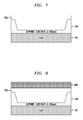
- the passivation layers 400A and 400B are removed after etching the cavity 600, and a volume of resin material 700 is deposited in the cavity 600 as shown in FIG. 7 .
- the resin material 700 is deposited by spinning on and planarizing an appropriate resin material.
- Poly methyl methacrylate (PMMA) is one example of an appropriate resin material. Embodiments, however, are not limited solely to the use of PMMA as a resin material. Instead, various other resin materials may be utilized.
- the cavity 600 defines a location for the lens structure 106 to be formed by reflowing the volume of resin material 700 deposited in the cavity 600.
- a layer of photoresist is spun on as shown in FIG. 8 .
- the photoresist 800 is patterned as shown in FIG. 9 .
- Reactive ion etching (RIE) or another suitable process is utilized to remove the remaining photoresist 800 and resin material 700 left open as shown in FIG. 10 .
- RIE reactive ion etching
- the next step is to reflow the resin material 700 to form the lens structure 106 as shown in FIG. 11 .
- the lens structure 106 is a plano-convex cylindrical lens.
- the processing steps described above, however, may be modified in a suitable manner to form other lens types and geometries, examples of which are described below.
- the n-contacts and p-contact are formed on the active semiconductor structure 102.
- a well-step-coverage SiO 2 passivation layer could be deposited by PECVD to preserve the active region sidewalls. Photolithography and wet etching processes can then be used to define the solder bump patterns.
- the solder bumps which may comprise tin (Sn),would then be electroplated onto the contacts.
- the cavity formed in substrate 104 may take on a wide variety of different shapes in other embodiments. Examples of the different cavity shapes and lens structures which may be formed therein are shown and described in conjunction with the cross-sectional views of FIGS. 12-20 .
- FIG. 12 illustrates a plano-concave cylindrical lens structure 1206 in the cavity 600 described above. If the cavity 600 were formed in a circular opening rather than a square opening 500 or other rectangular opening, the plano-concave cylindrical lens structure 1206 would be a plano-concave spherical lens structure.
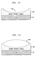
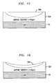
- FIG. 13 shows a substrate 1304 with a cavity 1300 formed in a circular opening.
- the cavity 1300 has a curved shape.
- the curved shape is defined by a concave bottom surface and curved sidewalls which extend upwards from edges of the bottom surface to an upper surface of the second side of the substrate 1304.
- the shape of the cavity 1300 defines a portion of a sphere with a plane parallel to the upper surface of the second side of the substrate 1304.
- FIG. 14 illustrates a biconvex lens structure 1406 formed in the cavity 1300
- FIG. 15 illustrates a plano-convex lens structure 1506 formed in the cavity 1300
- FIG. 16 illustrates a concavoconvex, periscopic convex, converging meniscus lens structure 1606 formed in the cavity 1300.
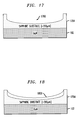
- FIG. 17 shows a substrate 1704 with a cavity 1700 formed in a circular opening.
- the cavity 1700 has a concave bottom surface and a plurality of sidewalls which extend upward from edges of the bottom surface to an upper surface of the second side of the substrate 1704.
- FIG. 17 illustrates sidewalls which are substantially perpendicular to the upper surface of the substrate 1704. In other embodiments, the sidewalls may be angled in a non-perpendicular fashion.
- FIG. 18 shows a convexoconcave, periscopic concave, diverging meniscus lens structure 1806 formed in the cavity 1700.
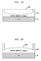
- FIG. 19 shows a convex cylindrical lens structure 1906 formed in a cavity with a cross-sectional shape similar to that of cavity 1700.
- the cavity in FIG. 19 is formed in a rectangular opening in the substrate 1904, rather than the circular opening as in FIG. 17 .
- the convex cylindrical lens structure 1906 is shown with the convex side of the lens structure facing towards the active semiconductor structure 102, rather than away from the active semiconductor structure 102 as in FIG. 1 and FIG. 11 .
- the convex side of the cylindrical lens structure 1906 in FIG. 19 is considered to be “face-down” while the convex side of the cylindrical lens structure 106 in FIG. 11 is considered to be “face-up.”
- various other lens structures described herein may similarly be formed “face-down” or “face-up” depending on the shape of a particular cavity.
- FIG. 20 shows a substrate 2004 with a cavity 2000 formed in a circular opening.
- the cavity 2000 has a convex bottom surface and a plurality of sidewalls which extend upward from edges of the bottom surface to an upper surface of the second side of the substrate 2004.
- FIG. 20 illustrates sidewalls which are substantially perpendicular to the upper surface of the substrate 2004. In other embodiments, the sidewalls may be angled in a non-perpendicular fashion.
- FIG. 21 shows a biconcave lens structure 2106 formed in the cavity 2000.
- lens structures may be formed in a face-down or face-up manner.
- a plano-concave lens structure may be formed in the cavity 2000 with the concave side of the lens facing towards the active semiconductor structure 102.
- Various other lens structures may be formed in the cavity 2000, including various meniscus lens structures and a concave cylindrical lens, where the concave side of the cylindrical lens faces towards the active semiconductor structure 102.
- a cavity may have stepped sidewalls, such that lens structures of varying diameters and/or varying types may be formed in the cavity.
- the term cavity as used herein is intended to be broadly construed so as to encompass these and other arrangements.
- lens structures can be utilized to focus light along desired paths.
- the particular cavity shapes and lens structures formed in a given semiconductor optical emitting device may be selected based on a particular application or intended use.
- Embodiments of the invention allow the formation of complex or compound lens structures within a cavity of the substrate.
- Complex and compound lens structures include a number of non-hemispherical lens structures such as those described above.
- the use of compound lens structures provides a number of distinct advantages relative to conventional techniques, including but not limited to: the formation of complex shapes and patterns of lens structures, improved optical characteristics such as reduced aberrations, suppressing internal reflections, and improved external quantum efficiency and optical coupling of light emitted from a semiconductor optical emitting device.
- FIG. 22 shows a top-down view of a wafer 2200.
- the wafer 2200 has an active semiconductor structure 2202 on which substrates 2204-1, 2204-2 and 2204-3 are formed.
- the substrates 2204-1, 2204-2 and 2204-3 each have a cavity in which lens structures 2206-1, 2206-2 and 2206-3 are formed, respectively.
- the cavities are defined to run a length of the wafer 2200 and are truncated before reaching the edge of the wafer 2200.
- the wafer 2200 may be separated into a number of individual die.
- FIG. 23 shows a top-down view of a single die formed from the wafer 2200.
- the left and right edges of the lens structure 106 are defined by the cavity in which the lens structure 106 is formed, while the top and bottom edges of the lens structure 106 are defined during separation of the wafer 2200 into the single die shown in FIG. 23 .
- the lens structure 106 may be formed by depositing a resin material into a cavity and reflowing the resin material to obtain the convex cylindrical lens geometry.
- the reflow process will pull the resin material deposited in the cavity toward edges of the cavity.
- the long trough cavities shown in the wafer 2200 of FIG. 22 are used to accurately achieve,for example, a convex or concave surface geometry over the length of the trough cavity before dicing or otherwise separating the wafer 2200 into individual die.
- the edges of the lens structure may be defined solely by the cavity in which it is formed.
- FIG. 24 shows a top-down view of a cylindrical lens structure 2406 formed in a rectangular cavity of a substrate 2404. The left, right, top and bottom edges of the cylindrical lens structure are defined by the rectangular cavity of the substrate 2404 in which the lens structure 2406 is formed.
- FIG. 25 shows a top-down view of a spherical lens structure 2506 formed in a circular cavity of a substrate 2504. The edges of the spherical lens structure 2506 are defined by the circular cavity of the substrate 2504 in which the lens structure 2506 is formed.
- the spherical lens may be one of a number of spherical geometries including but not limited to biconvex, biconcave, plano-convex, plano-concave and meniscus geometries.
- FIG. 26 shows a substrate 2604 with a number of lens structures formed in cavities therein.
- the substrate 2604 has four distinct cavities in which lens structures 2606-1 through 2606-4 are formed.
- a combination of cylindrical lens structures 2606-1 and 2606-2 and spherical lens structures 2606-3 and 2606-4 are formed.
- Various other combinations are possible, including a substrate with more or less than four cavities, as well as more or less than two different cavity shapes.
- a given cavity may be shaped such that two or more lens structures are formed in a single cavity.
- semiconductor optical emitting devices such as those described above can be implemented in the form of integrated circuits.
- identical die are typically formed in a repeated pattern on a surface of a semiconductor wafer.
- Each die includes circuitry as described herein, and may include other structures or circuits.
- the individual die are cut or diced from the wafer, then packaged as an integrated circuit.
- One skilled in the art would know how to dice wafers and package die to produce integrated circuits. Integrated circuits so manufactured are considered embodiments of the invention.
- FIG. 27 shows one example of an integrated circuit embodiment of the invention.
- an integrated circuit 2700 comprises an array 2702 of SELs 100 each configured as previously described in conjunction with FIG. 1 .
- Control circuitry 2704 is coupled to the array 2702 of SELsand is configured to controlgeneration of light by those SELs.
- the integrated circuit 2700 may be implemented in a lighting system, an electronic display or another type of system or device.
- a given optical emitting device integrated circuit 2700 may be incorporated into a processing device 2800 as illustrated in FIG. 28 .
- a processing device may comprise a laptop or tablet computer, a mobile telephone, an e-reader or another type of processing device that utilizes one or more SEL integrated circuits to provide back lighting or for other functions.
- the optical emitting device integrated circuit 2700 is coupled to a processor 2810 that controls generation of light by the corresponding array of SELs.
- the processor 2810 may comprise, for example, a microprocessor, an application-specific integrated circuit (ASIC), a field-programmable gate array (FPGA), a central processing unit (CPU), an arithmetic logic unit (ALU), a digital signal processor (DSP), or other similar processing device component, as well as other types and arrangements of circuitry, in any combination.
- ASIC application-specific integrated circuit
- FPGA field-programmable gate array
- CPU central processing unit
- ALU arithmetic logic unit
- DSP digital signal processor
- the processor 2810 is coupled to a memory 2812.
- the memory 2812 stores software code for execution by the processor 2810 in implementing portions of the functionality of the processing device 2800.
- a given such memory that stores software code for execution by a corresponding processor is an example of what is more generally referred to herein as a computer-readable medium or other type of computer program product having computer program code embodied therein, and may comprise, for example, electronic memory such as random access memory (RAM) or read-only memory (ROM), magnetic memory, optical memory, or other types of storage devices in any combination.
- the processor may comprise portions or combinations of a microprocessor, ASIC, FPGA, CPU, ALU, DSP or other circuitry. Such circuitry components utilized to implement the processor may comprise one or more integrated circuits.
- integrated circuit 2700 and processing device 2800 as shown in respective FIGS. 27 and 28 are exemplary only, and in other embodiments integrated circuits and processing devices may include other elements in addition to or in place of those specifically shown, including one or more elements of a type commonly found in conventional implementations of such circuits and devices.
Landscapes
- Physics & Mathematics (AREA)
- Condensed Matter Physics & Semiconductors (AREA)
- General Physics & Mathematics (AREA)
- Electromagnetism (AREA)
- Optics & Photonics (AREA)
- Led Device Packages (AREA)
- Led Devices (AREA)
- Semiconductor Lasers (AREA)
Applications Claiming Priority (1)
| Application Number | Priority Date | Filing Date | Title |
|---|---|---|---|
| US13/898,964 US20140348197A1 (en) | 2013-05-21 | 2013-05-21 | Semiconductor optical emitting device with lens structure formed in a cavity of a substrate of the device |
Publications (1)
| Publication Number | Publication Date |
|---|---|
| EP2806470A1 true EP2806470A1 (de) | 2014-11-26 |
Family
ID=50732957
Family Applications (1)
| Application Number | Title | Priority Date | Filing Date |
|---|---|---|---|
| EP14169226.9A Withdrawn EP2806470A1 (de) | 2013-05-21 | 2014-05-21 | Licht emittierende Halbleitervorrichtung mit in einem Hohlraum eines Substrats der Vorrichtung geformter Linsenstruktur |
Country Status (6)
| Country | Link |
|---|---|
| US (1) | US20140348197A1 (de) |
| EP (1) | EP2806470A1 (de) |
| JP (1) | JP2014229897A (de) |
| KR (1) | KR20140136858A (de) |
| CN (1) | CN104184043A (de) |
| TW (1) | TW201445841A (de) |
Cited By (1)
| Publication number | Priority date | Publication date | Assignee | Title |
|---|---|---|---|---|
| WO2020136349A1 (fr) * | 2018-12-28 | 2020-07-02 | Aledia | Dispositif optoélectronique à diode électroluminescente micrométrique ou nanométrique surmontée d'une lentille optique |
Families Citing this family (5)
| Publication number | Priority date | Publication date | Assignee | Title |
|---|---|---|---|---|
| WO2016146658A1 (en) | 2015-03-16 | 2016-09-22 | Plessey Semiconductors Limited | Light emitting diode chip and a method for the manufacture of a light emitting diode chip |
| CA2995815C (en) * | 2015-06-22 | 2021-08-24 | The Brigham And Women's Hospital, Inc | Home evaluation of the quality of semen samples |
| JP2017059742A (ja) * | 2015-09-18 | 2017-03-23 | 株式会社デンソー | 発光装置 |
| DE102019100410A1 (de) * | 2019-01-09 | 2020-07-09 | Osram Opto Semiconductors Gmbh | Volumenemitter und Verfahren zu dessen Herstellung |
| CN113748360A (zh) * | 2020-01-16 | 2021-12-03 | 索尼半导体解决方案公司 | 光源装置、光源装置的制造方法以及电子设备 |
Citations (5)
| Publication number | Priority date | Publication date | Assignee | Title |
|---|---|---|---|---|
| JPS5669879A (en) * | 1979-11-12 | 1981-06-11 | Toshiba Corp | Semiconductor luminous device with lens |
| US20080179615A1 (en) * | 2007-01-26 | 2008-07-31 | Chi-Hung Kao | Light-emitting diode device |
| US20080197365A1 (en) * | 2007-02-16 | 2008-08-21 | Yu-Nung Shen | Light emitting device |
| US20130048940A1 (en) * | 2011-08-26 | 2013-02-28 | Micron Technology, Inc. | Solid state radiation transducers and methods of manufacturing |
| KR20130038558A (ko) * | 2011-10-10 | 2013-04-18 | 엘지이노텍 주식회사 | 발광소자 |
Family Cites Families (4)
| Publication number | Priority date | Publication date | Assignee | Title |
|---|---|---|---|---|
| US5718830A (en) * | 1996-02-15 | 1998-02-17 | Lucent Technologies Inc. | Method for making microlenses |
| JP2006179511A (ja) * | 2004-12-20 | 2006-07-06 | Sumitomo Electric Ind Ltd | 発光装置 |
| JP2007080996A (ja) * | 2005-09-13 | 2007-03-29 | Sony Corp | GaN系半導体発光素子及びその製造方法 |
| CN107256915A (zh) * | 2009-09-18 | 2017-10-17 | 天空公司 | 发光二极管器件 |
-
2013
- 2013-05-21 US US13/898,964 patent/US20140348197A1/en not_active Abandoned
- 2013-11-12 TW TW102141125A patent/TW201445841A/zh unknown
- 2013-12-03 CN CN201310637389.6A patent/CN104184043A/zh active Pending
- 2013-12-06 KR KR20130151479A patent/KR20140136858A/ko not_active Withdrawn
-
2014
- 2014-02-07 JP JP2014021979A patent/JP2014229897A/ja active Pending
- 2014-05-21 EP EP14169226.9A patent/EP2806470A1/de not_active Withdrawn
Patent Citations (5)
| Publication number | Priority date | Publication date | Assignee | Title |
|---|---|---|---|---|
| JPS5669879A (en) * | 1979-11-12 | 1981-06-11 | Toshiba Corp | Semiconductor luminous device with lens |
| US20080179615A1 (en) * | 2007-01-26 | 2008-07-31 | Chi-Hung Kao | Light-emitting diode device |
| US20080197365A1 (en) * | 2007-02-16 | 2008-08-21 | Yu-Nung Shen | Light emitting device |
| US20130048940A1 (en) * | 2011-08-26 | 2013-02-28 | Micron Technology, Inc. | Solid state radiation transducers and methods of manufacturing |
| KR20130038558A (ko) * | 2011-10-10 | 2013-04-18 | 엘지이노텍 주식회사 | 발광소자 |
Cited By (3)
| Publication number | Priority date | Publication date | Assignee | Title |
|---|---|---|---|---|
| WO2020136349A1 (fr) * | 2018-12-28 | 2020-07-02 | Aledia | Dispositif optoélectronique à diode électroluminescente micrométrique ou nanométrique surmontée d'une lentille optique |
| FR3091413A1 (fr) * | 2018-12-28 | 2020-07-03 | Aledia | Dispositif optoélectronique à diode électroluminescente micrométrique ou nanométrique surmontée d’une lentille optique |
| US12414416B2 (en) | 2018-12-28 | 2025-09-09 | Aledia | Optoelectronic device with micrometric or nanometric light-emitting diode on which an optical lens is mounted |
Also Published As
| Publication number | Publication date |
|---|---|
| US20140348197A1 (en) | 2014-11-27 |
| JP2014229897A (ja) | 2014-12-08 |
| KR20140136858A (ko) | 2014-12-01 |
| CN104184043A (zh) | 2014-12-03 |
| TW201445841A (zh) | 2014-12-01 |
Similar Documents
| Publication | Publication Date | Title |
|---|---|---|
| KR102075172B1 (ko) | 금속화된 측벽을 가진 반도체 발광 디바이스 | |
| EP2806470A1 (de) | Licht emittierende Halbleitervorrichtung mit in einem Hohlraum eines Substrats der Vorrichtung geformter Linsenstruktur | |
| TWI870017B (zh) | 發光元件 | |
| US10381507B2 (en) | Light emitting diode chip and a method for the manufacture of a light emitting diode chip | |
| US9461204B2 (en) | Light-emitting devices on textured substrates | |
| EP2943986B1 (de) | Leuchtdiode mit ausgeformtem aufwachssubstrat zur horizontalemission und verfahren zu seiner herstellung | |
| EP3149781B1 (de) | Lichtemittierende vorrichtung mit strukturiertem substrat | |
| EP2408025A1 (de) | Leuchtdiode und verfahren zu ihrer herstellung | |
| EP2672790A2 (de) | Vorrichtungsmodul | |
| CN111164766A (zh) | 一种制作半导体发光元件的方法 | |
| CN109791962A (zh) | 氮化物半导体紫外线发光元件的制造方法和氮化物半导体紫外线发光元件 | |
| WO2017154975A1 (ja) | 半導体発光装置 | |
| EP2626916A1 (de) | Lichtemittierende diode und herstellungsverfahren dafür | |
| US9105807B2 (en) | Semiconductor optical emitting device with grooved substrate providing multiple angled light emission paths | |
| CN106505130A (zh) | 一种led芯片的图形化基板及其制备方法 | |
| EP2943985B1 (de) | Geformte led für effizientere lichtauskopplung | |
| KR101766588B1 (ko) | 수직형 발광다이오드 소자 및 이의 제조방법 | |
| CN118073495A (zh) | 一种发光二极管及其制备方法、显示面板 |
Legal Events
| Date | Code | Title | Description |
|---|---|---|---|
| PUAI | Public reference made under article 153(3) epc to a published international application that has entered the european phase |
Free format text: ORIGINAL CODE: 0009012 |
|
| 17P | Request for examination filed |
Effective date: 20140521 |
|
| AK | Designated contracting states |
Kind code of ref document: A1 Designated state(s): AL AT BE BG CH CY CZ DE DK EE ES FI FR GB GR HR HU IE IS IT LI LT LU LV MC MK MT NL NO PL PT RO RS SE SI SK SM TR |
|
| AX | Request for extension of the european patent |
Extension state: BA ME |
|
| STAA | Information on the status of an ep patent application or granted ep patent |
Free format text: STATUS: THE APPLICATION IS DEEMED TO BE WITHDRAWN |
|
| 18D | Application deemed to be withdrawn |
Effective date: 20150527 |