EP2806444B1 - Vorrichtung und Verfahren zur Unterbrechung des Stroms in einem Leistungsübertragungs- oder Verteilungssystem - Google Patents
Vorrichtung und Verfahren zur Unterbrechung des Stroms in einem Leistungsübertragungs- oder Verteilungssystem Download PDFInfo
- Publication number
- EP2806444B1 EP2806444B1 EP14168486.0A EP14168486A EP2806444B1 EP 2806444 B1 EP2806444 B1 EP 2806444B1 EP 14168486 A EP14168486 A EP 14168486A EP 2806444 B1 EP2806444 B1 EP 2806444B1
- Authority
- EP
- European Patent Office
- Prior art keywords
- current
- sic mosfet
- time point
- sic
- circuit breaker
- Prior art date
- Legal status (The legal status is an assumption and is not a legal conclusion. Google has not performed a legal analysis and makes no representation as to the accuracy of the status listed.)
- Active
Links
Images


Classifications
-
- H—ELECTRICITY
- H03—ELECTRONIC CIRCUITRY
- H03K—PULSE TECHNIQUE
- H03K17/00—Electronic switching or gating, i.e. not by contact-making and –breaking
- H03K17/51—Electronic switching or gating, i.e. not by contact-making and –breaking characterised by the components used
- H03K17/56—Electronic switching or gating, i.e. not by contact-making and –breaking characterised by the components used by the use, as active elements, of semiconductor devices
- H03K17/687—Electronic switching or gating, i.e. not by contact-making and –breaking characterised by the components used by the use, as active elements, of semiconductor devices the devices being field-effect transistors
- H03K17/6871—Electronic switching or gating, i.e. not by contact-making and –breaking characterised by the components used by the use, as active elements, of semiconductor devices the devices being field-effect transistors the output circuit comprising more than one controlled field-effect transistor
-
- H—ELECTRICITY
- H01—ELECTRIC ELEMENTS
- H01H—ELECTRIC SWITCHES; RELAYS; SELECTORS; EMERGENCY PROTECTIVE DEVICES
- H01H9/00—Details of switching devices, not covered by groups H01H1/00 - H01H7/00
- H01H9/54—Circuit arrangements not adapted to a particular application of the switching device and for which no provision exists elsewhere
- H01H9/548—Electromechanical and static switch connected in series
-
- H—ELECTRICITY
- H01—ELECTRIC ELEMENTS
- H01H—ELECTRIC SWITCHES; RELAYS; SELECTORS; EMERGENCY PROTECTIVE DEVICES
- H01H33/00—High-tension or heavy-current switches with arc-extinguishing or arc-preventing means
- H01H33/02—Details
- H01H33/59—Circuit arrangements not adapted to a particular application of the switch and not otherwise provided for, e.g. for ensuring operation of the switch at a predetermined point in the AC cycle
- H01H33/596—Circuit arrangements not adapted to a particular application of the switch and not otherwise provided for, e.g. for ensuring operation of the switch at a predetermined point in the AC cycle for interrupting DC
-
- H—ELECTRICITY
- H02—GENERATION; CONVERSION OR DISTRIBUTION OF ELECTRIC POWER
- H02H—EMERGENCY PROTECTIVE CIRCUIT ARRANGEMENTS
- H02H3/00—Emergency protective circuit arrangements for automatic disconnection directly responsive to an undesired change from normal electric working condition with or without subsequent reconnection ; integrated protection
- H02H3/08—Emergency protective circuit arrangements for automatic disconnection directly responsive to an undesired change from normal electric working condition with or without subsequent reconnection ; integrated protection responsive to excess current
- H02H3/087—Emergency protective circuit arrangements for automatic disconnection directly responsive to an undesired change from normal electric working condition with or without subsequent reconnection ; integrated protection responsive to excess current for DC applications
-
- H—ELECTRICITY
- H03—ELECTRONIC CIRCUITRY
- H03K—PULSE TECHNIQUE
- H03K17/00—Electronic switching or gating, i.e. not by contact-making and –breaking
- H03K17/12—Modifications for increasing the maximum permissible switched current
- H03K17/122—Modifications for increasing the maximum permissible switched current in field-effect transistor switches
-
- H—ELECTRICITY
- H03—ELECTRONIC CIRCUITRY
- H03K—PULSE TECHNIQUE
- H03K17/00—Electronic switching or gating, i.e. not by contact-making and –breaking
- H03K17/51—Electronic switching or gating, i.e. not by contact-making and –breaking characterised by the components used
- H03K17/56—Electronic switching or gating, i.e. not by contact-making and –breaking characterised by the components used by the use, as active elements, of semiconductor devices
- H03K17/72—Electronic switching or gating, i.e. not by contact-making and –breaking characterised by the components used by the use, as active elements, of semiconductor devices having more than two PN junctions; having more than three electrodes; having more than one electrode connected to the same conductivity region
- H03K17/725—Electronic switching or gating, i.e. not by contact-making and –breaking characterised by the components used by the use, as active elements, of semiconductor devices having more than two PN junctions; having more than three electrodes; having more than one electrode connected to the same conductivity region for AC voltages or currents
Definitions
- Embodiments of the invention relate generally to devices and methods to break current, and in particular, to direct current (DC) circuit breakers applied in high-voltage direct current (HVDC) systems, medium-voltage direct current (MVDC) power transmission or distribution systems, or the like.
- DC direct current
- HVDC or MVDC systems In recent years, the interest in HVDC or MVDC systems has been revived. In those HVDC or MVDC systems, DC circuit breakers are necessary to make the HVDC or MVDC systems more flexible and reliable for many applications such as multi-terminal HVDC grids, MVDC power distribution for subsea electrification, and marine MVDC power transmission and so on.
- the DC circuit breakers need to be developed and validated at full scale to operate a multi-terminal HVDC or MVDC grid protection for fast interruption time and low loss.
- a DC circuit breaker consists of silicon insulated gate bipolar transistors (IGBTs), which are controlled to interrupt HVDC or MVDC currents within a few milliseconds.
- IGBTs silicon insulated gate bipolar transistors
- the traditional silicon IGBTs may consume lots of energy during the energy transmission process, which decreases efficiency.
- heat sinks need to be arranged on the silicon IGBTs.
- WO 2011/057675 discloses a breaking device for HVDC transmission lines comprising an auxiliary breaker in series with a high speed switch and in parallel with a main breaker.
- the auxiliary breaker includes one or more power semiconductor switches.
- a direct current (DC) circuit breaker having capabilities of low conduction loss and faster switching speed for power transmission or distribution system.
- the DC circuit breaker includes a current sensor for sensing current of a system, a controller, a physical switch, and multiple switch modules.
- the multiple switch modules are electrically coupled to the current sensor and the physical switch in series.
- Each switch module includes multiple base elements electrically coupled in parallel.
- Each base element includes a first silicon carbide (SiC) metal-oxide-semiconductor field-effect transistor (MOSFET) and a second SiC MOSFET electrically coupled in an opposite series connection mode.
- the first and second SiC MOSFETs are configured in a synchronous rectification mode by channel reverse conduction control.
- the controller controls the multiple switch modules to connect current in the system, and break current of the multiple switch modules according to sensed current signals from the current sensor.
- a current connecting method for the DC circuit breaker includes turning on the physical switch at a first time point; turning on the first SiC MOSFET of each base element at a second time point after a predetermined time interval from the first time point; and turning on the second SiC MOSFET of each base element at a third time point after a predetermined time interval from the second time point.
- the current direction is from the first SiC MOSFET to the second SiC MOSFET of each base element.
- a current breaking method for the DC circuit breaker includes turning off the first SiC MOSFET of each base element at a first time point; turning off the physical switch at a second time point after a predetermined time interval from the first time point; and turning off the second SiC MOSFET of each base element at a third time point after a predetermined time interval from the second time point.
- the current direction is from the first SiC MOSFET to the second SiC MOSFET of each base element.
- Embodiments of the invention relate to a direct current (DC) circuit breaker for power transmission or distribution system.
- the DC circuit breaker includes a current sensor for sensing current of a system, a controller, a physical switch, and multiple switch modules.
- the multiple switch modules are electrically coupled to the current sensor and the physical switch in series.
- Each switch module includes multiple base elements electrically coupled in parallel.
- Each base element includes a first silicon carbide (SiC) metal-oxide-semiconductor field-effect transistor (MOSFET) and a second SiC MOSFET electrically coupled in an opposite series connection mode.
- the first and second SiC MOSFETs are configured in a synchronous rectification mode by channel reverse conduction control.
- the controller controls the multiple switch modules to connect current in the system, and break current of the multiple switch modules according to sensed current signals from the current sensor.
- FIG. 1 a block diagram of a DC circuit breaker 100 according to one embodiment is shown.
- the DC circuit breaker 100 can be applied in any power transmission or distribution systems, such as high-voltage direct current (HVDC) systems, medium-voltage direct current (MVDC) systems, etc., to break current when the current flowing therein is not within a predetermined range or when the power transmission systems fall into some situations which need to quickly cut the current off.
- HVDC high-voltage direct current
- MVDC medium-voltage direct current
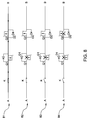
- the DC circuit breaker 100 includes two terminals 'A' and 'B', a mechanical switch K, a current limiter L, a current sensor CS, a current breaking unit 120, and a controller 140.
- the current limiter L is an inductor.
- the controller 140 may be any type of programmable devices, such as a micro-controller, a micro control unit (MCU), a digital signal processor (DSP), etc.
- the two terminals 'A' and 'B' are used to electrically couple the DC circuit breaker 100 into a current transmission line of a power transmission system (not shown).
- the current sensor CS is used to sense current flowing through the DC circuit breaker 100.
- the controller 140 is used to receive sensed current signals from the current sensor CS and control the mechanical switch K and the current breaking unit 120 according to the sensed current signals. In a normal working status, the controller 140 switches the mechanical switch K and the current breaking unit 120 on to ensure the current can be transmitted through the DC circuit breaker 100. In an abnormal working status, for example when the sensed current signal is greater than a predetermined maximum value, such as 2kA, the controller 140 switches the mechanical switch K and the current breaking unit 120 off to interrupt the current flowing through the DC circuit breaker 100.
- the current breaking unit 120 is used to provide a fast current interruption and the mechanical switch K is used to provide a physical current interruption. In some embodiments, the mechanical switch K also can be controlled manually.
- the current breaking unit 120 includes at least one switch module 12 electrically coupled in series.
- the number of the series-connected switch modules 12 is determined according to the current value flowing through the DC circuit breaker 100. When the current flowing through the DC circuit breaker 100 is getting greater, the number of the series-connected switch modules 12 is getting greater accordingly, and vice versa.
- Each switch module 12 further electrically couples to a non-linear resister R in parallel. The non-linear resister R can help balance the voltage sharing, as well as absorb the fault current breaking energy. Every switch module 12 has a similar function; therefore only one switch module 12 will be described in detail in the following paragraphs.
- the switch module 12 may include a plurality of base elements 122 electrically coupled in parallel.
- the number of the parallel-connected base elements 122 is also determined according to the current value flowing through the DC circuit breaker 100.
- the illustrated embodiment shows an exemplary embodiment which includes three parallel-connected base elements 122. Every base element 122 has a similar function; therefore only one base element 122 will be described in detail in the following paragraphs.
- the base element 122 includes a first silicon carbide (SiC) metal-oxide-semiconductor field-effect transistor (MOSFET) Q1 and a second SiC MOSFET Q2 electrically coupled in an opposite series connection mode.
- the first SiC MOSFET Q1 further includes a free-wheeling diode D1.
- the second SiC MOSFET Q2 further includes a free-wheeling diode D2.
- the drain terminal of the first SiC MOSFET Q1 is connected to a first terminal 'a'
- the source terminal of the first SiC MOSFET Q1 is connected to the source terminal of the second SiC MOSFET Q2
- the gate terminal of the first SiC MOSFET Q1 is used to receive control commands from the controller 140
- the cathode of the diode D1 is connected to the drain terminal of the first SiC MOSFET Q1
- the anode of the diode D1 is connected to the source terminal of the first SiC MOSFET Q1.
- the drain terminal of the second SiC MOSFET Q2 is connected to a second terminal 'b', the gate terminal of the second SiC MOSFET Q2 is used to receive control commands from the controller 140, the cathode of the diode D2 is connected to the drain terminal of the second SiC MOSFET Q2, the anode of the diode D2 is connected to the source terminal of the second SiC MOSFET Q2.
- there may be more first SiC MOSFETs Q1 connected in series to handle a greater current or there may be more second SiC MOSFETs Q2 connected in series to handle a greater current.
- the number of the first SiC MOSFETs Q1 and the number of the second SiC MOSFET Q2 may vary according to actual current requirements.
- the diode D1 and D2 can either be SiC MOSFET parasitical diodes or external paralleled diodes.
- the controller 140 outputs control commands to the mechanical switch K and the switch modules 12 according to predetermined programs.
- the controller 140 outputs those control commands according to a startup signal from the power transmission or distribution system.
- a flowchart of a DC current connecting method 30 for the switch modules 12 and the mechanical switch K is shown in FIG. 3 as an exemplary embodiment.
- the current direction is from the terminal 'A' to 'B'.
- the DC current connecting method 30 includes the following steps.
- step 31 the mechanical switch K is turned on at a first time point T1 according to a control command S K shown as a command wave 41 in FIG. 4 .
- This mechanical switch K is used to provide a physical connection between the two terminals 'A' and 'B'. In other embodiments, the mechanical switch K may be other types of physical switches.
- a physical connection between the two terminals 'A' and 'B' is finished firstly.
- FIG. 5 an initial status 51 is shown, and a status 52 of the step 31 is shown. In the initial status 51, the mechanical switch K and the switch modules 12 are opened. In this status 52, the mechanical switch K is turned on, but due to the MOSFETs Q1 and Q2 are not turned on, there is no current flowing through the DC circuit breaker 100 yet.
- step 32 after a predetermined time interval from the first time point T1, such as after about 1 microseconds to 1000 microseconds, all of the first SiC MOSFETs Q1 are turned on at a second time point T2 according to a control command S Q1 shown as a command wave 42 in FIG. 4 .
- a status 53 of the step 32 is shown. In this status 53, the mechanical switch K is turned on, the first SiC MOSFETs Q1 are turned on as well, but the second SiC MOSFETs Q2 are not turned on yet.
- the current will pass through the mechanical switch K, pass through the first SiC MOSFETs Q1 from the drain terminal to the source terminal thereof, and pass through the diode D2 of the second SiC MOSFETs Q2 (see arrows from 'A' to 'B').
- the power loss may be large in the second SiC MOSFETs Q2 because of the diode D2 may consume power greater.
- this SiC MOSFET configuration only consumes about 0.2-0.5 times power loss.
- the switch response speed of the SiC MOSFEF configuration is faster about 5-10 times compared with the conventional Si IGBT configuration.
- step 33 after a predetermined time interval from the second time point T2, such as after about 1 microseconds to 1000 microseconds, all of the second SiC MOSFETs Q2 are turned on at a third time point T3 according to a control command S Q2 shown as a command wave 43 in FIG. 4 .
- a status 54 of the step 33 is shown. In this status 54, the mechanical switch K is turned on, the first SiC MOSFETs Q1 are turned on, and the second SiC MOSFETs Q2 are turned on as well.
- the current will pass through the mechanical switch K, pass through the first SiC MOSFETs Q1 from the drain terminal to the source terminal thereof, and pass through the second SiC MOSFETs Q2 from the source terminal to the drain terminal thereof (see arrows from 'A' to 'B').
- This is due to the SiC MOSFETs having synchronous rectification (SR) mode by a channel reverse conduction control, which can operate current through the SiC MOSFETs along a less loss channel, which may further reduce about 17% power loss after performing this step 33.
- SR synchronous rectification
- each of the SiC MOSFETs Q1 and Q2 can be a reversed channel conduction from the drain terminal to the source terminal or from the source terminal to the drain terminal but not passing through the diodes D1 and D2, which can make the current pass through the less-loss device channel. Therefore, compared with the conventional DC circuit breakers, the SiC MOSFETs Q1 and Q2 will consume less energy during the conduction process. Thus, by using the SiC MOSFETs Q1 and Q2 instead of the conventional semiconductor switches, such as silicon IGBTs, the energy transfer efficiency is increased.
- the SiC MOSFETs Q1 and Q2 consume less energy, the heat generated by the SiC MOSFETs Q1 and Q2 is less than the heat generated by the conventional semiconductor switches. Furthermore, the SiC MOSFET can handle higher operation temperature (such as bigger than 175 degrees Celsius). Therefore, the number or volume of the heat sinks (not shown) arranged on the SiC MOSFETs Q1 and Q2 may be less than the number or volume of the heat sinks that are required for a conventional semiconductor switches.
- step 32 and step 33 is reversed.
- the second SiC MOSFETs Q2 are turned on first and then the first SiC MOSFETs Q1 are turned on.
- the controller 140 outputs control commands to the mechanical switch K and the switch modules 12 according to predetermined programs.
- the controller 140 outputs those control commands according to the current sensing signals sensed by the current sensor CS, for example when a current sensing signal is greater than a predetermined value.
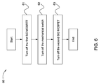
- a flowchart of a DC current breaking method 60 for the switch modules 12 and the mechanical switch K is shown in FIG. 6 as an exemplary embodiment. Herein, the current direction is from the terminal 'A' to 'B'.
- the DC current breaking method 60 includes the following steps.
- step 61 the first SiC MOSFETs Q1 is turned off at a fourth time point T4 according to the control command S Q1 shown as a command wave 72 in FIG. 7 .
- a normal working status 81 (same as the status 54 shown in FIG. 5 ) is shown, and a status 82 of the step 61 is shown.
- the SiC MOSFETs Q1 are turned off, therefore the current is interrupted immediately. Due to the switch time of the SiC MOSFET is very short, may be take only a few milliseconds, which can satisfy the quick switch requirement of the power transmission or distribution system.
- step 62 after a predetermined time interval from the fourth time point T4, such as after about 1 microseconds to 1000 microseconds, the mechanical switch K is turned off at a fifth time point T5 according to the control command S K shown in FIG. 7 . After the mechanical switch K is turned off, the physical connection between the two terminals 'A' and 'B' is cut off. Referring to FIG. 8 , a status 83 of the step 62 is shown. In this status 52, the mechanical switch K is turned off, and the first MOSFETs Q1 are turned off.
- step 63 after a predetermined time interval from the fifth time point T5, such as after about 1 microseconds to 1000 microseconds, all of the second SiC MOSFETs Q2 are turned off at a sixth time point T6 according to the control command S Q2 showing in FIG. 7 .
- a status 84 of the step 63 is shown.
- the mechanical switch K is turned off, the first SiC MOSFETs Q1 is turned off, and the second SiC MOSFETs Q2 is turned off as well. Therefore, the current connecting points are all cut off finally and back to the initial status 51.
- the power transmission system can be recovered according to the control performed by the DC current connecting method 30.
- step 61 and step 63 is reversed.
- the second SiC MOSFETs Q2 is turned off firstly and then the first SiC MOSFETs Q1 is turned off after the mechanical switch K is turned off.
Landscapes
- Engineering & Computer Science (AREA)
- Power Engineering (AREA)
- Driving Mechanisms And Operating Circuits Of Arc-Extinguishing High-Tension Switches (AREA)
- Keying Circuit Devices (AREA)
Claims (15)
- Gleichstrom(DC)-Unterbrecher (100), der aufweist:einen Stromsensor (CS) zur Erfassung eines Stroms eines Systems;eine Steuereinrichtung (140);einen physischen Schalter (K), der mit dem Stromsensor (CS) in Reihe elektrisch verbunden ist; undein erstes Schaltmodul (12), das mit dem physischen Schalter (K) in Reihe elektrisch verbunden ist, wobei das erste Schaltmodul (12) ein erstes Basiselement (122) aufweist;dadurch gekennzeichnet, dass das erste Basiselement (122) aufweist:einen ersten Siliziumkarbid(SiC)-Metall-Oxid-Halbleiter-Feldeffektortransistor (MOSFET) (Q1); undeinen zweiten SiC-MOSFET (Q2), der mit dem ersten SiC-MOSFET (Q1) in einem gegensinnig in Reihe geschalteten Modus elektrisch verbunden ist;wobei der erste und der zweite SiC-MOSFET (Q1, Q2) durch eine Kanalrückwärtsleitungssteuerung in einem synchronen Gleichrichtungsmodus konfiguriert sind; undwobei die Steuerung (140) eingerichtet ist, um den ersten und den zweiten SiC-MOSFET (Q1, Q2) zu steuern, um entsprechend erfassten Stromsignalen von dem Stromsensor (CS) Strom in dem System anzuschließen und Strom des ersten und des zweiten SiC-MOSFET (Q1, Q2) zu unterbrechen, wobei die Stromrichtung von dem ersten SiC-MOSFET (Q1) zu dem zweiten SiC-MOSFET (Q2) des ersten Basiselementes (122) verläuft.
- DC-Unterbrecher (100) nach Anspruch 1, der ferner ein oder mehrere zweite Schaltmodule (12) aufweist, die mit dem ersten Schaltmodul (12) in Reihe elektrisch verbunden sind, wobei jedes zweite Schaltmodul (12) die gleiche Konfiguration mit dem ersten Schaltmodul (12) aufweist.
- DC-Unterbrecher (100) nach Anspruch 1 oder Anspruch 2, wobei das erste Schaltmodul (12) ferner ein oder mehrere zweite Basiselemente (122) aufweist, die mit dem ersten Basiselement (122) elektrisch parallel geschaltet sind, wobei jedes zweite Basiselement (122) die gleiche Konfiguration mit dem ersten Basiselement (122) aufweist.
- DC-Unterbrecher (100) nach einem beliebigen vorhergehenden Anspruch, wobei der physische Schalter ein mechanischer Schalter (K) ist.
- DC-Unterbrecher (100) nach einem beliebigen vorhergehenden Anspruch, wobei der physische Schalter (K) durch die Steuerung (140) gesteuert ist.
- DC-Unterbrecher (100) nach einem beliebigen vorhergehenden Anspruch, der ferner einen Strombegrenzer (L) aufweist, der mit dem ersten Schaltmodul (12) in Reihe elektrisch verbunden ist.
- DC-Unterbrecher (100) nach Anspruch 6, wobei der Strombegrenzer eine Spule (L) ist.
- DC-Unterbrecher (100) nach einem beliebigen vorhergehenden Anspruch, der ferner einen nicht linearen Widerstand (R) aufweist, der mit dem ersten Schaltmodul (12) elektrisch parallel geschaltet ist.
- DC-Unterbrecher (100) nach einem beliebigen vorhergehenden Anspruch, wobei das erste Basiselement (122) ferner einen oder mehrere SiC-MOSFETs aufweist, die mit dem ersten SiC-MOSFET (Q1) mit der gleichen Stromrichtung elektrisch verbunden sind.
- DC-Unterbrecher (100) nach einem beliebigen vorhergehenden Anspruch, wobei das erste Basiselement (122) ferner einen oder mehrere SiC-MOSFETs aufweist, die mit dem zweiten SiC-MOSFET (Q2) mit der gleichen Stromrichtung elektrisch verbunden sind.
- DC-Unterbrecher (100) nach einem beliebigen vorhergehenden Anspruch, wobei ein Drain-Anschluss des ersten SiC-MOSFETs (Q1) mit einem ersten Anschluss ("a") verbunden ist, ein Source-Anschluss des ersten SiC-MOSFETs (Q1) mit einem Source-Anschluss des zweiten SiC-MOSFETs (Q2) verbunden ist, ein Gate-Anschluss des ersten SiC-MOSFETs (Q1) verwendet wird, um Steuerbefehle von der Steuerung (140) zu empfangen, eine Kathode einer ersten Diode (D1) mit dem Drain-Anschluss des ersten SiC-MOSFETs (Q1) verbunden ist, eine Anode der erste Diode (D1) mit dem Source-Anschluss des ersten SiC-MOSFETs (Q1) verbunden ist, ein Drain-Anschluss des zweiten SiC-MOSFETs (Q2) mit einem zweiten Anschluss ("b") verbunden ist, ein Gate-Anschluss des zweiten SiC-MOSFETs (Q2) verwendet wird, um Steuerbefehle von der Steuerung (140) zu empfangen, eine Kathode einer zweiten Diode (D2) mit dem Drain-Anschluss des zweiten SiC-MOSFETs (Q2) verbunden ist, eine Anode der zweiten Diode (D2) mit dem Source-Anschluss des zweiten SiC-MOSFETs (Q2) verbunden ist.
- Stromanschlussverfahren für den DC-Unterbrecher nach einem beliebigen vorhergehenden Anspruch, wobei das Verfahren die Schritte aufweist:Einschalten des physischen Schalters (K) in einem ersten Zeitpunkt;Einschalten des ersten SiC-MOSFETS (Q1) des ersten Basiselementes (122) in einem zweiten Zeitpunkt nach einem vorbestimmten Zeitintervall ausgehend von dem ersten Zeitpunkt; undEinschalten des zweiten SiC-MOSFETS (Q2) des ersten Basiselementes (122) in einem dritten Zeitpunkt nach einem vorbestimmten Zeitintervall ausgehend von dem zweiten Zeitpunkt;wobei die Stromrichtung von dem ersten SiC-MOSFET (Q1) zu dem zweiten SiC-MOSFET (Q2) des ersten Basiselementes (122) verläuft.
- Stromanschlussverfahren nach Anspruch 12, wobei das Zeitintervall zwischen dem ersten Zeitpunkt und dem zweiten Zeitpunkt von etwa 1 Mikrosekunde bis etwa 1000 Mikrosekunden beträgt und/oder das Zeitintervall zwischen dem zweiten Zeitpunkt und dem dritten Zeitpunkt von etwa 1 Mikrosekunde bis etwa 1000 Mikrosekunden beträgt.
- Stromunterbrechungsverfahren für den DC-Unterbrecher nach einem beliebigen der Ansprüche 1 bis 11, wobei das Verfahren die Schritte aufweist:Abschalten des ersten SiC-MOSFETs (Q1) des ersten Basiselementes (122) in einem ersten Zeitpunkt;Abschalten des physischen Schalters (K) in einem zweiten Zeitpunkt nach einem vorbestimmten Zeitintervall ausgehend von dem ersten Zeitpunkt; undAbschalten des zweiten SiC-MOSFETs (Q2) des ersten Basiselementes (122) in einem dritten Zeitpunkt nach einem vorbestimmten Zeitintervall ausgehend von dem zweiten Zeitpunkt;wobei die Stromrichtung von dem ersten SiC-MOSFET (Q1) zu dem zweiten SiC-MOSFET (Q2) des ersten Basiselementes (122) verläuft.
- Stromunterbrechungsverfahren nach Anspruch 14, wobei das Zeitintervall zwischen dem ersten Zeitpunkt und dem zweiten Zeitpunkt von etwa 1 Mikrosekunde bis etwa 1000 Mikrosekunden beträgt und/oder das Zeitintervall zwischen dem zweiten Zeitpunkt und dem dritten Zeitpunkt von etwa 1 Mikrosekunde bis zu etwa 1000 Mikrosekunden beträgt.
Applications Claiming Priority (1)
| Application Number | Priority Date | Filing Date | Title |
|---|---|---|---|
| CN201310188777.0A CN104184108B (zh) | 2013-05-21 | 2013-05-21 | 直流断路器及其控制方法 |
Publications (2)
| Publication Number | Publication Date |
|---|---|
| EP2806444A1 EP2806444A1 (de) | 2014-11-26 |
| EP2806444B1 true EP2806444B1 (de) | 2016-09-14 |
Family
ID=50721654
Family Applications (1)
| Application Number | Title | Priority Date | Filing Date |
|---|---|---|---|
| EP14168486.0A Active EP2806444B1 (de) | 2013-05-21 | 2014-05-15 | Vorrichtung und Verfahren zur Unterbrechung des Stroms in einem Leistungsübertragungs- oder Verteilungssystem |
Country Status (5)
| Country | Link |
|---|---|
| US (1) | US10187056B2 (de) |
| EP (1) | EP2806444B1 (de) |
| CN (1) | CN104184108B (de) |
| CA (1) | CA2851011A1 (de) |
| IN (1) | IN2014CH02426A (de) |
Families Citing this family (19)
| Publication number | Priority date | Publication date | Assignee | Title |
|---|---|---|---|---|
| CN103684002B (zh) * | 2012-09-24 | 2016-12-21 | 通用电气公司 | 能量转换系统 |
| CN104348342B (zh) * | 2013-08-02 | 2019-05-31 | 通用电气公司 | 电能变换系统和方法 |
| US9343897B2 (en) * | 2014-07-07 | 2016-05-17 | General Electric Company | Circuit breaker system and method |
| KR102167948B1 (ko) | 2014-12-31 | 2020-10-20 | 엘에스일렉트릭(주) | 직류차단기 및 이의 차단방법 |
| CN104600693B (zh) * | 2015-01-07 | 2017-01-18 | 中国科学院电工研究所 | 用于直流电网的储能—断路器 |
| CN106253243B (zh) * | 2016-08-09 | 2018-09-28 | 南京南瑞继保电气有限公司 | 一种高压直流断路器的合闸控制方法 |
| CN106230413A (zh) * | 2016-08-18 | 2016-12-14 | 平高集团有限公司 | 一种混合型高压直流断路器及其功率单元 |
| DE102016117003A1 (de) * | 2016-09-09 | 2018-03-15 | Eaton Industries (Austria) Gmbh | Schutzschaltgerät |
| CN107171292B (zh) * | 2017-07-12 | 2019-06-07 | 重庆大学 | 一种基于SiC MOSFET直流固态断路器抑制关断过电压的装置 |
| US10171069B1 (en) | 2018-01-26 | 2019-01-01 | General Electric Company | Switch controller for adaptive reverse conduction control in switch devices |
| WO2019169041A1 (en) * | 2018-02-27 | 2019-09-06 | Ideal Power Inc. | Hvdc/mvdc systems and methods with low-loss fully-bidirectional bjt circuit breakers |
| GB2574038A (en) * | 2018-05-24 | 2019-11-27 | Entrust Microgrid Llp | Two-stage switching mechanism for use in a DC circuit |
| KR102652596B1 (ko) * | 2018-08-27 | 2024-04-01 | 엘에스일렉트릭(주) | 양방향 반도체 차단기 |
| CN110854829B (zh) * | 2019-12-06 | 2024-12-17 | 华北电力科学研究院有限责任公司 | 直流断路器主动保护系统 |
| EP3879548B1 (de) * | 2020-03-10 | 2022-12-21 | ABB Schweiz AG | Fehlerstrombegrenzerschutzschalter |
| US12160096B2 (en) | 2020-04-14 | 2024-12-03 | Drexel University | Solid-state circuit breaker based on a wireless coupling and resonant circuit for MVDC systems |
| WO2022194442A1 (de) * | 2021-03-18 | 2022-09-22 | Preh Gmbh | Vorrichtung zur sicherung eines aus einer gleichspannungsquelle gespeisten elektrischen verbrauchers gegen einen überstrom |
| CN113437731B (zh) * | 2021-07-14 | 2023-03-14 | 东北林业大学 | 一种基于高速机械开关的限流型混合直流断路器 |
| JP2025056473A (ja) * | 2023-09-27 | 2025-04-08 | 株式会社村田製作所 | 電源装置及びプログラム |
Family Cites Families (18)
| Publication number | Priority date | Publication date | Assignee | Title |
|---|---|---|---|---|
| US5339210A (en) | 1992-07-22 | 1994-08-16 | General Electric Company | DC circuit interrupter |
| US5463252A (en) | 1993-10-01 | 1995-10-31 | Westinghouse Electric Corp. | Modular solid state relay |
| SE510597C2 (sv) * | 1997-03-24 | 1999-06-07 | Asea Brown Boveri | Anläggning för överföring av elektrisk effekt |
| US6952335B2 (en) * | 2002-03-22 | 2005-10-04 | Virginia Tech Intellectual Properties, Inc. | Solid-state DC circuit breaker |
| US20060238936A1 (en) * | 2005-04-25 | 2006-10-26 | Blanchard Richard A | Apparatus and method for transient blocking employing relays |
| NO329609B1 (no) | 2008-02-19 | 2010-11-22 | Wartsila Norway As | Elektronisk DC-kretsbryter |
| US8729739B2 (en) * | 2010-04-28 | 2014-05-20 | The United States Of America As Represented By The Secretary Of The Navy | Bi-directional circuit breaker |
| US8742628B2 (en) * | 2009-04-30 | 2014-06-03 | The United States Of America As Represented By The Secretary Of The Army | Solid state circuit breaker |
| US8004806B2 (en) | 2009-05-04 | 2011-08-23 | United Silicon Carbide, Inc. | Solid-state disconnect device |
| CN102549907B (zh) | 2009-07-31 | 2015-01-21 | 阿尔斯通技术有限公司 | 具有主动故障电流限制的变换器 |
| ES2420531T3 (es) | 2009-08-13 | 2013-08-23 | Abb Research Ltd. | Disyuntor híbrido |
| EP2494571B1 (de) | 2009-10-27 | 2013-12-11 | ABB Technology AG | Hochspannungs-gleichstrom-schutzschalter und steuervorrichtung für einen hochspannungs-gleichstrom-schutzschalter |
| AU2009355281B2 (en) * | 2009-11-16 | 2014-01-16 | Hitachi Energy Ltd | Device and method to break the current of a power transmission or distribution line and current limiting arrangement |
| ES2503557T3 (es) * | 2010-05-11 | 2014-10-07 | Abb Technology Ag | Disyuntor de corriente continua de alta tensión |
| WO2011157306A1 (en) | 2010-06-14 | 2011-12-22 | Abb Research Ltd | Breaker failure protection of hvdc circuit breakers |
| EP2639805B1 (de) | 2010-12-23 | 2014-12-10 | ABB Technology AG | Verfahren, Schutzschalter und Schalteinheit zum Abschalten von Hochspannungsgleichströmen |
| US8890019B2 (en) | 2011-02-05 | 2014-11-18 | Roger Webster Faulkner | Commutating circuit breaker |
| US20140029152A1 (en) * | 2012-03-30 | 2014-01-30 | Semisouth Laboratories, Inc. | Solid-state circuit breakers |
-
2013
- 2013-05-21 CN CN201310188777.0A patent/CN104184108B/zh active Active
-
2014
- 2014-05-08 CA CA 2851011 patent/CA2851011A1/en not_active Abandoned
- 2014-05-15 IN IN2426CH2014 patent/IN2014CH02426A/en unknown
- 2014-05-15 EP EP14168486.0A patent/EP2806444B1/de active Active
- 2014-05-21 US US14/283,333 patent/US10187056B2/en active Active
Non-Patent Citations (1)
| Title |
|---|
| None * |
Also Published As
| Publication number | Publication date |
|---|---|
| CA2851011A1 (en) | 2014-11-21 |
| EP2806444A1 (de) | 2014-11-26 |
| CN104184108B (zh) | 2018-08-10 |
| IN2014CH02426A (de) | 2015-07-03 |
| CN104184108A (zh) | 2014-12-03 |
| US20140346891A1 (en) | 2014-11-27 |
| US10187056B2 (en) | 2019-01-22 |
Similar Documents
| Publication | Publication Date | Title |
|---|---|---|
| EP2806444B1 (de) | Vorrichtung und Verfahren zur Unterbrechung des Stroms in einem Leistungsübertragungs- oder Verteilungssystem | |
| US7741883B2 (en) | Method of switching and switching device for solid state power controller applications | |
| CN110808572B (zh) | 开关装置 | |
| US11025245B2 (en) | Power conversion device | |
| US9755630B2 (en) | Solid-state circuit breakers and related circuits | |
| EP2916440B1 (de) | Elektronische schaltung | |
| US9543751B2 (en) | Self-powered DC solid state circuit breakers | |
| EP3468026B1 (de) | Stromwandler | |
| EP3029821B1 (de) | Halbleiterbauelement und stromumwandlungsvorrichtung | |
| CN109950866B (zh) | 电流切断器 | |
| CN107579649B (zh) | 用于功率开关管的驱动装置 | |
| CN105474545A (zh) | 半导体开关串 | |
| CN104348360A (zh) | 电压转换控制器及电压转换电路 | |
| EP3357160A1 (de) | Halbleiterschaltstrang | |
| WO2015090365A1 (en) | Integrated series converter and circuit breaker in a power system | |
| CN110661236B (zh) | 断路器装置及系统 | |
| Sander et al. | A novel current-injection based design for HVDC circuit breakers | |
| EP3057232A1 (de) | Schutzschaltervorrichtung | |
| CN113544953A (zh) | 开关的驱动装置 | |
| EP3343583A1 (de) | Gleichstromschutzschalter | |
| US20130114314A1 (en) | Converter system and power electronic system comprising such converter systems | |
| CN107408897B (zh) | 电力变换装置以及电动机装置 | |
| CN104885363A (zh) | 半导体开关设备 | |
| JP6447944B2 (ja) | 電力変換装置、及びそれを用いたパワーコンディショナ | |
| Prigmore et al. | An IGCT-based electronic circuit breaker design for a 12.47 kV distribution system |
Legal Events
| Date | Code | Title | Description |
|---|---|---|---|
| PUAI | Public reference made under article 153(3) epc to a published international application that has entered the european phase |
Free format text: ORIGINAL CODE: 0009012 |
|
| 17P | Request for examination filed |
Effective date: 20140515 |
|
| AK | Designated contracting states |
Kind code of ref document: A1 Designated state(s): AL AT BE BG CH CY CZ DE DK EE ES FI FR GB GR HR HU IE IS IT LI LT LU LV MC MK MT NL NO PL PT RO RS SE SI SK SM TR |
|
| AX | Request for extension of the european patent |
Extension state: BA ME |
|
| R17P | Request for examination filed (corrected) |
Effective date: 20150513 |
|
| RBV | Designated contracting states (corrected) |
Designated state(s): AL AT BE BG CH CY CZ DE DK EE ES FI FR GB GR HR HU IE IS IT LI LT LU LV MC MK MT NL NO PL PT RO RS SE SI SK SM TR |
|
| GRAP | Despatch of communication of intention to grant a patent |
Free format text: ORIGINAL CODE: EPIDOSNIGR1 |
|
| RIC1 | Information provided on ipc code assigned before grant |
Ipc: H01H 9/54 20060101AFI20160309BHEP Ipc: H01H 33/59 20060101ALI20160309BHEP Ipc: H03K 17/687 20060101ALN20160309BHEP |
|
| INTG | Intention to grant announced |
Effective date: 20160406 |
|
| RIC1 | Information provided on ipc code assigned before grant |
Ipc: H03K 17/687 20060101ALN20160329BHEP Ipc: H01H 9/54 20060101AFI20160329BHEP Ipc: H01H 33/59 20060101ALI20160329BHEP |
|
| GRAJ | Information related to disapproval of communication of intention to grant by the applicant or resumption of examination proceedings by the epo deleted |
Free format text: ORIGINAL CODE: EPIDOSDIGR1 |
|
| GRAR | Information related to intention to grant a patent recorded |
Free format text: ORIGINAL CODE: EPIDOSNIGR71 |
|
| GRAS | Grant fee paid |
Free format text: ORIGINAL CODE: EPIDOSNIGR3 |
|
| GRAA | (expected) grant |
Free format text: ORIGINAL CODE: 0009210 |
|
| INTC | Intention to grant announced (deleted) | ||
| RIC1 | Information provided on ipc code assigned before grant |
Ipc: H01H 9/54 20060101AFI20160720BHEP Ipc: H03K 17/687 20060101ALN20160720BHEP Ipc: H01H 33/59 20060101ALI20160720BHEP |
|
| INTG | Intention to grant announced |
Effective date: 20160729 |
|
| AK | Designated contracting states |
Kind code of ref document: B1 Designated state(s): AL AT BE BG CH CY CZ DE DK EE ES FI FR GB GR HR HU IE IS IT LI LT LU LV MC MK MT NL NO PL PT RO RS SE SI SK SM TR |
|
| REG | Reference to a national code |
Ref country code: GB Ref legal event code: FG4D |
|
| REG | Reference to a national code |
Ref country code: CH Ref legal event code: EP |
|
| REG | Reference to a national code |
Ref country code: IE Ref legal event code: FG4D |
|
| REG | Reference to a national code |
Ref country code: AT Ref legal event code: REF Ref document number: 829791 Country of ref document: AT Kind code of ref document: T Effective date: 20161015 |
|
| REG | Reference to a national code |
Ref country code: DE Ref legal event code: R096 Ref document number: 602014003579 Country of ref document: DE |
|
| REG | Reference to a national code |
Ref country code: LT Ref legal event code: MG4D |
|
| REG | Reference to a national code |
Ref country code: NL Ref legal event code: MP Effective date: 20160914 |
|
| PG25 | Lapsed in a contracting state [announced via postgrant information from national office to epo] |
Ref country code: LT Free format text: LAPSE BECAUSE OF FAILURE TO SUBMIT A TRANSLATION OF THE DESCRIPTION OR TO PAY THE FEE WITHIN THE PRESCRIBED TIME-LIMIT Effective date: 20160914 Ref country code: RS Free format text: LAPSE BECAUSE OF FAILURE TO SUBMIT A TRANSLATION OF THE DESCRIPTION OR TO PAY THE FEE WITHIN THE PRESCRIBED TIME-LIMIT Effective date: 20160914 Ref country code: NO Free format text: LAPSE BECAUSE OF FAILURE TO SUBMIT A TRANSLATION OF THE DESCRIPTION OR TO PAY THE FEE WITHIN THE PRESCRIBED TIME-LIMIT Effective date: 20161214 Ref country code: HR Free format text: LAPSE BECAUSE OF FAILURE TO SUBMIT A TRANSLATION OF THE DESCRIPTION OR TO PAY THE FEE WITHIN THE PRESCRIBED TIME-LIMIT Effective date: 20160914 Ref country code: FI Free format text: LAPSE BECAUSE OF FAILURE TO SUBMIT A TRANSLATION OF THE DESCRIPTION OR TO PAY THE FEE WITHIN THE PRESCRIBED TIME-LIMIT Effective date: 20160914 |
|
| REG | Reference to a national code |
Ref country code: AT Ref legal event code: MK05 Ref document number: 829791 Country of ref document: AT Kind code of ref document: T Effective date: 20160914 |
|
| PG25 | Lapsed in a contracting state [announced via postgrant information from national office to epo] |
Ref country code: SE Free format text: LAPSE BECAUSE OF FAILURE TO SUBMIT A TRANSLATION OF THE DESCRIPTION OR TO PAY THE FEE WITHIN THE PRESCRIBED TIME-LIMIT Effective date: 20160914 Ref country code: NL Free format text: LAPSE BECAUSE OF FAILURE TO SUBMIT A TRANSLATION OF THE DESCRIPTION OR TO PAY THE FEE WITHIN THE PRESCRIBED TIME-LIMIT Effective date: 20160914 Ref country code: LV Free format text: LAPSE BECAUSE OF FAILURE TO SUBMIT A TRANSLATION OF THE DESCRIPTION OR TO PAY THE FEE WITHIN THE PRESCRIBED TIME-LIMIT Effective date: 20160914 Ref country code: GR Free format text: LAPSE BECAUSE OF FAILURE TO SUBMIT A TRANSLATION OF THE DESCRIPTION OR TO PAY THE FEE WITHIN THE PRESCRIBED TIME-LIMIT Effective date: 20161215 |
|
| PG25 | Lapsed in a contracting state [announced via postgrant information from national office to epo] |
Ref country code: RO Free format text: LAPSE BECAUSE OF FAILURE TO SUBMIT A TRANSLATION OF THE DESCRIPTION OR TO PAY THE FEE WITHIN THE PRESCRIBED TIME-LIMIT Effective date: 20160914 Ref country code: EE Free format text: LAPSE BECAUSE OF FAILURE TO SUBMIT A TRANSLATION OF THE DESCRIPTION OR TO PAY THE FEE WITHIN THE PRESCRIBED TIME-LIMIT Effective date: 20160914 |
|
| REG | Reference to a national code |
Ref country code: FR Ref legal event code: PLFP Year of fee payment: 4 |
|
| PG25 | Lapsed in a contracting state [announced via postgrant information from national office to epo] |
Ref country code: BG Free format text: LAPSE BECAUSE OF FAILURE TO SUBMIT A TRANSLATION OF THE DESCRIPTION OR TO PAY THE FEE WITHIN THE PRESCRIBED TIME-LIMIT Effective date: 20161214 Ref country code: ES Free format text: LAPSE BECAUSE OF FAILURE TO SUBMIT A TRANSLATION OF THE DESCRIPTION OR TO PAY THE FEE WITHIN THE PRESCRIBED TIME-LIMIT Effective date: 20160914 Ref country code: CZ Free format text: LAPSE BECAUSE OF FAILURE TO SUBMIT A TRANSLATION OF THE DESCRIPTION OR TO PAY THE FEE WITHIN THE PRESCRIBED TIME-LIMIT Effective date: 20160914 Ref country code: BE Free format text: LAPSE BECAUSE OF FAILURE TO SUBMIT A TRANSLATION OF THE DESCRIPTION OR TO PAY THE FEE WITHIN THE PRESCRIBED TIME-LIMIT Effective date: 20160914 Ref country code: SK Free format text: LAPSE BECAUSE OF FAILURE TO SUBMIT A TRANSLATION OF THE DESCRIPTION OR TO PAY THE FEE WITHIN THE PRESCRIBED TIME-LIMIT Effective date: 20160914 Ref country code: PL Free format text: LAPSE BECAUSE OF FAILURE TO SUBMIT A TRANSLATION OF THE DESCRIPTION OR TO PAY THE FEE WITHIN THE PRESCRIBED TIME-LIMIT Effective date: 20160914 Ref country code: IS Free format text: LAPSE BECAUSE OF FAILURE TO SUBMIT A TRANSLATION OF THE DESCRIPTION OR TO PAY THE FEE WITHIN THE PRESCRIBED TIME-LIMIT Effective date: 20170114 Ref country code: SM Free format text: LAPSE BECAUSE OF FAILURE TO SUBMIT A TRANSLATION OF THE DESCRIPTION OR TO PAY THE FEE WITHIN THE PRESCRIBED TIME-LIMIT Effective date: 20160914 Ref country code: PT Free format text: LAPSE BECAUSE OF FAILURE TO SUBMIT A TRANSLATION OF THE DESCRIPTION OR TO PAY THE FEE WITHIN THE PRESCRIBED TIME-LIMIT Effective date: 20170116 Ref country code: AT Free format text: LAPSE BECAUSE OF FAILURE TO SUBMIT A TRANSLATION OF THE DESCRIPTION OR TO PAY THE FEE WITHIN THE PRESCRIBED TIME-LIMIT Effective date: 20160914 |
|
| REG | Reference to a national code |
Ref country code: DE Ref legal event code: R097 Ref document number: 602014003579 Country of ref document: DE |
|
| PG25 | Lapsed in a contracting state [announced via postgrant information from national office to epo] |
Ref country code: IT Free format text: LAPSE BECAUSE OF FAILURE TO SUBMIT A TRANSLATION OF THE DESCRIPTION OR TO PAY THE FEE WITHIN THE PRESCRIBED TIME-LIMIT Effective date: 20160914 |
|
| PLBE | No opposition filed within time limit |
Free format text: ORIGINAL CODE: 0009261 |
|
| STAA | Information on the status of an ep patent application or granted ep patent |
Free format text: STATUS: NO OPPOSITION FILED WITHIN TIME LIMIT |
|
| PG25 | Lapsed in a contracting state [announced via postgrant information from national office to epo] |
Ref country code: DK Free format text: LAPSE BECAUSE OF FAILURE TO SUBMIT A TRANSLATION OF THE DESCRIPTION OR TO PAY THE FEE WITHIN THE PRESCRIBED TIME-LIMIT Effective date: 20160914 |
|
| 26N | No opposition filed |
Effective date: 20170615 |
|
| PG25 | Lapsed in a contracting state [announced via postgrant information from national office to epo] |
Ref country code: LU Free format text: LAPSE BECAUSE OF NON-PAYMENT OF DUE FEES Effective date: 20170531 |
|
| PG25 | Lapsed in a contracting state [announced via postgrant information from national office to epo] |
Ref country code: SI Free format text: LAPSE BECAUSE OF FAILURE TO SUBMIT A TRANSLATION OF THE DESCRIPTION OR TO PAY THE FEE WITHIN THE PRESCRIBED TIME-LIMIT Effective date: 20160914 |
|
| REG | Reference to a national code |
Ref country code: CH Ref legal event code: PL |
|
| PG25 | Lapsed in a contracting state [announced via postgrant information from national office to epo] |
Ref country code: MC Free format text: LAPSE BECAUSE OF FAILURE TO SUBMIT A TRANSLATION OF THE DESCRIPTION OR TO PAY THE FEE WITHIN THE PRESCRIBED TIME-LIMIT Effective date: 20160914 |
|
| REG | Reference to a national code |
Ref country code: IE Ref legal event code: MM4A |
|
| PG25 | Lapsed in a contracting state [announced via postgrant information from national office to epo] |
Ref country code: CH Free format text: LAPSE BECAUSE OF NON-PAYMENT OF DUE FEES Effective date: 20170531 Ref country code: LI Free format text: LAPSE BECAUSE OF NON-PAYMENT OF DUE FEES Effective date: 20170531 |
|
| PG25 | Lapsed in a contracting state [announced via postgrant information from national office to epo] |
Ref country code: LU Free format text: LAPSE BECAUSE OF NON-PAYMENT OF DUE FEES Effective date: 20170515 |
|
| PG25 | Lapsed in a contracting state [announced via postgrant information from national office to epo] |
Ref country code: IE Free format text: LAPSE BECAUSE OF NON-PAYMENT OF DUE FEES Effective date: 20170515 |
|
| REG | Reference to a national code |
Ref country code: FR Ref legal event code: PLFP Year of fee payment: 5 |
|
| PG25 | Lapsed in a contracting state [announced via postgrant information from national office to epo] |
Ref country code: MT Free format text: LAPSE BECAUSE OF NON-PAYMENT OF DUE FEES Effective date: 20170515 |
|
| PG25 | Lapsed in a contracting state [announced via postgrant information from national office to epo] |
Ref country code: AL Free format text: LAPSE BECAUSE OF FAILURE TO SUBMIT A TRANSLATION OF THE DESCRIPTION OR TO PAY THE FEE WITHIN THE PRESCRIBED TIME-LIMIT Effective date: 20160914 |
|
| PG25 | Lapsed in a contracting state [announced via postgrant information from national office to epo] |
Ref country code: HU Free format text: LAPSE BECAUSE OF FAILURE TO SUBMIT A TRANSLATION OF THE DESCRIPTION OR TO PAY THE FEE WITHIN THE PRESCRIBED TIME-LIMIT; INVALID AB INITIO Effective date: 20140515 |
|
| PG25 | Lapsed in a contracting state [announced via postgrant information from national office to epo] |
Ref country code: CY Free format text: LAPSE BECAUSE OF FAILURE TO SUBMIT A TRANSLATION OF THE DESCRIPTION OR TO PAY THE FEE WITHIN THE PRESCRIBED TIME-LIMIT Effective date: 20160914 |
|
| PG25 | Lapsed in a contracting state [announced via postgrant information from national office to epo] |
Ref country code: MK Free format text: LAPSE BECAUSE OF FAILURE TO SUBMIT A TRANSLATION OF THE DESCRIPTION OR TO PAY THE FEE WITHIN THE PRESCRIBED TIME-LIMIT Effective date: 20160914 |
|
| PG25 | Lapsed in a contracting state [announced via postgrant information from national office to epo] |
Ref country code: TR Free format text: LAPSE BECAUSE OF FAILURE TO SUBMIT A TRANSLATION OF THE DESCRIPTION OR TO PAY THE FEE WITHIN THE PRESCRIBED TIME-LIMIT Effective date: 20160914 |
|
| PGFP | Annual fee paid to national office [announced via postgrant information from national office to epo] |
Ref country code: DE Payment date: 20250423 Year of fee payment: 12 |
|
| PGFP | Annual fee paid to national office [announced via postgrant information from national office to epo] |
Ref country code: GB Payment date: 20250423 Year of fee payment: 12 |
|
| PGFP | Annual fee paid to national office [announced via postgrant information from national office to epo] |
Ref country code: FR Payment date: 20250423 Year of fee payment: 12 |