EP2806315B1 - A method for fabricating a coloured component for a watch - Google Patents
A method for fabricating a coloured component for a watch Download PDFInfo
- Publication number
- EP2806315B1 EP2806315B1 EP14169164.2A EP14169164A EP2806315B1 EP 2806315 B1 EP2806315 B1 EP 2806315B1 EP 14169164 A EP14169164 A EP 14169164A EP 2806315 B1 EP2806315 B1 EP 2806315B1
- Authority
- EP
- European Patent Office
- Prior art keywords
- thin film
- pattern
- boundary
- wafer
- moon
- Prior art date
- Legal status (The legal status is an assumption and is not a legal conclusion. Google has not performed a legal analysis and makes no representation as to the accuracy of the status listed.)
- Not-in-force
Links
Images



Classifications
-
- G—PHYSICS
- G04—HOROLOGY
- G04B—MECHANICALLY-DRIVEN CLOCKS OR WATCHES; MECHANICAL PARTS OF CLOCKS OR WATCHES IN GENERAL; TIME PIECES USING THE POSITION OF THE SUN, MOON OR STARS
- G04B19/00—Indicating the time by visual means
- G04B19/26—Clocks or watches with indicators for tides, for the phases of the moon, or the like
- G04B19/268—Clocks or watches with indicators for tides, for the phases of the moon, or the like with indicators for the phases of the moon
-
- G—PHYSICS
- G04—HOROLOGY
- G04D—APPARATUS OR TOOLS SPECIALLY DESIGNED FOR MAKING OR MAINTAINING CLOCKS OR WATCHES
- G04D3/00—Watchmakers' or watch-repairers' machines or tools for working materials
- G04D3/0074—Watchmakers' or watch-repairers' machines or tools for working materials for treatment of the material, e.g. surface treatment
- G04D3/0092—Watchmakers' or watch-repairers' machines or tools for working materials for treatment of the material, e.g. surface treatment for components of the time-indicating mechanism, e.g. dials
-
- C—CHEMISTRY; METALLURGY
- C23—COATING METALLIC MATERIAL; COATING MATERIAL WITH METALLIC MATERIAL; CHEMICAL SURFACE TREATMENT; DIFFUSION TREATMENT OF METALLIC MATERIAL; COATING BY VACUUM EVAPORATION, BY SPUTTERING, BY ION IMPLANTATION OR BY CHEMICAL VAPOUR DEPOSITION, IN GENERAL; INHIBITING CORROSION OF METALLIC MATERIAL OR INCRUSTATION IN GENERAL
- C23C—COATING METALLIC MATERIAL; COATING MATERIAL WITH METALLIC MATERIAL; SURFACE TREATMENT OF METALLIC MATERIAL BY DIFFUSION INTO THE SURFACE, BY CHEMICAL CONVERSION OR SUBSTITUTION; COATING BY VACUUM EVAPORATION, BY SPUTTERING, BY ION IMPLANTATION OR BY CHEMICAL VAPOUR DEPOSITION, IN GENERAL
- C23C14/00—Coating by vacuum evaporation, by sputtering or by ion implantation of the coating forming material
- C23C14/22—Coating by vacuum evaporation, by sputtering or by ion implantation of the coating forming material characterised by the process of coating
- C23C14/34—Sputtering
- C23C14/35—Sputtering by application of a magnetic field, e.g. magnetron sputtering
-
- G—PHYSICS
- G03—PHOTOGRAPHY; CINEMATOGRAPHY; ANALOGOUS TECHNIQUES USING WAVES OTHER THAN OPTICAL WAVES; ELECTROGRAPHY; HOLOGRAPHY
- G03F—PHOTOMECHANICAL PRODUCTION OF TEXTURED OR PATTERNED SURFACES, e.g. FOR PRINTING, FOR PROCESSING OF SEMICONDUCTOR DEVICES; MATERIALS THEREFOR; ORIGINALS THEREFOR; APPARATUS SPECIALLY ADAPTED THEREFOR
- G03F7/00—Photomechanical, e.g. photolithographic, production of textured or patterned surfaces, e.g. printing surfaces; Materials therefor, e.g. comprising photoresists; Apparatus specially adapted therefor
- G03F7/20—Exposure; Apparatus therefor
-
- G—PHYSICS
- G03—PHOTOGRAPHY; CINEMATOGRAPHY; ANALOGOUS TECHNIQUES USING WAVES OTHER THAN OPTICAL WAVES; ELECTROGRAPHY; HOLOGRAPHY
- G03F—PHOTOMECHANICAL PRODUCTION OF TEXTURED OR PATTERNED SURFACES, e.g. FOR PRINTING, FOR PROCESSING OF SEMICONDUCTOR DEVICES; MATERIALS THEREFOR; ORIGINALS THEREFOR; APPARATUS SPECIALLY ADAPTED THEREFOR
- G03F7/00—Photomechanical, e.g. photolithographic, production of textured or patterned surfaces, e.g. printing surfaces; Materials therefor, e.g. comprising photoresists; Apparatus specially adapted therefor
- G03F7/26—Processing photosensitive materials; Apparatus therefor
-
- G—PHYSICS
- G04—HOROLOGY
- G04B—MECHANICALLY-DRIVEN CLOCKS OR WATCHES; MECHANICAL PARTS OF CLOCKS OR WATCHES IN GENERAL; TIME PIECES USING THE POSITION OF THE SUN, MOON OR STARS
- G04B19/00—Indicating the time by visual means
- G04B19/06—Dials
- G04B19/12—Selection of materials for dials or graduations markings
Definitions
- the present invention relates to a method of fabricating a component for use in a watch and in particular, coloured watch components such as those used in a moon-phase display of the watch.
- Certain watches contain coloured components in the dial section of the watch, for instance, to form part of a moon-phase display for indicating the phase of the moon at any given time.
- the colour characteristic of such watch components is of high quality and precision so as to improve the visual contrast and hence readability of the indicator, as well as enhancing the ornamental and aesthetic qualities of the indicator.
- the colour characteristics of the watch components may be provided by virtue of the natural colours of the materials forming the components.
- materials with natural colour characteristics typically include metals, metal alloys and metal oxides which tend to have good mechanical properties and are suitably durable for use as watch components;
- a gold colour may be provided by electroplated gold, and, a blue colour on the hour and minute hands may be provided by an oxidised steel material at a well controlled temperature.
- the disadvantage with utilising the natural colours of these types of materials suitable for forming the watch display components is that the range of suitable materials, and colours available, is limited.
- a broader range of colour characteristics of the watch display components may be provided by painting the components a desired range of colours.
- the quality and sharpness of the contours of coloured patterns painted on the watch display materials are unsuitable for use in high-rend watches.
- gold may be used as a wafer for a moon-phase indicator of a watch with a diamond-like carbon film coating whereby a laser beam is used to remove the diamond like carbon in the desired areas of the watch display to expose the gold wafer. Whilst this method tends to produce a high quality moon-phase display, the processing costs are relatively high and the process efficiency is relatively low.
- an invention which comprises a decorated article formed by a process of coating a silicon substrate with silicon compounds to form coloured patterns on the decorated article.
- the process of coating the silicon compounds on to the silicon substrate as taught by this document is not performed for the purpose of achieving relatively high quality and sharpness in the contours of the colored patterns on the decorated article. Instead, the objective and effect of this is to produce a decorated article in which the coloured patterns formed by the silicon compound coatings possess high chemical resistance and superior mechanical strength.
- the present invention seeks to alleviate at least one of the problems discussed above in relation to the prior art.
- the present invention provides a method of fabricating a component for use in a watch as set out in Claim 1.
- the wafer may include an opaque material. More preferably, the wafer may include a silicon wafer.
- the step of depositing the first thin film on the wafer may include use of at least one of a plasma-enhanced chemical vapour deposition (PECVD) process and a low pressure chemical vapour deposition (LPCVD) process.
- PECVD plasma-enhanced chemical vapour deposition
- LPCVD low pressure chemical vapour deposition
- the first thin film may include a silicon nitride material. Also preferably, the first thin film may include a refractive index greater than 2.
- the step of processing the region within the boundary of the pattern may include depositing a metal material within the boundary of the pattern which is indicative of the second colour characteristic.
- this may involve the use of a magnetron sputtering deposition or an electron-beam evaporation deposition process.
- the step of processing the region within the boundary of the pattern may include removing at least some of the first thin film within the boundary of the pattern, for instance by HF solution or dry etching, and then depositing a second thin film therein which is suitably adapted to produce the second colour characteristic.
- the second thin film may be deposited using a plasma-enhanced chemical vapour deposition (PECVD) process.
- PECVD plasma-enhanced chemical vapour deposition
- the second thin film may also include a silicon nitride material.
- the step of processing the region within the boundary of the pattern may include depositing a second thin film within the region within the boundary of the pattern without removing any of the first thin film within the boundary of the pattern such that the second thin film either alone or in combination with the first thin film may be adapted to produce the second colour characteristic.
- the second thin film may be deposited using a plasma-enhanced chemical vapour deposition (PECVD) process.
- PECVD plasma-enhanced chemical vapour deposition
- the second thin film may also include a silicon nitride material.
- the step of processing the region within the boundary of the pattern may include thinning the first thin film within the boundary of the pattern to a desired thickness suitable for producing the second colour characteristic.
- the thinning may be performed for instance using HF solution or dry etching
- the use of photolithography may assist in defining the boundary of the pattern with relatively high precision and definition - i.e. typically in the order of a few hundred nanometres - such that deposition of materials such as metals, ceramics, thin films and the like on to the wafer within the boundaries of a pattern may be of suitably high quality and accuracy for application in ornamentation of luxury watches and the like.
- components with durability and optical precision may be mass produced using photolithographic MEMS technologies.
- the pattern may include a moon or a star shape.
- a method is provided in accordance with embodiments of the present invention for use in fabricating a watch component (1) as shown in Fig. 1 having multiple colour characteristics.
- the watch component (1) fabricated in accordance with these embodiments includes a moon-phase display having a blue coloured background (11), and gold coloured moon (12) and stars (13) pattern. It should be understood that other types of watch components with other types of colour characteristics may of course also be fabricated using this apparatus.
- the apparatus includes a computerised controller (400) having an input and output user interface which is configured for controlling a thin film deposition apparatus (404), a photolithography apparatus (403), a sputtering apparatus (402) and an etching apparatus (401).
- a computerised controller 400 having an input and output user interface which is configured for controlling a thin film deposition apparatus (404), a photolithography apparatus (403), a sputtering apparatus (402) and an etching apparatus (401).
- An opaque silicon wafer (300) is used to form the base of the moon-phase display (1) as shown in Fig. 3A .
- a first thin film of silicon nitride (301) is deposited on to the silicon wafer (300) as shown in Fig. 3B with the first thin film (301) having a thickness in the sub-nanometer to micron range so as to reflect certain wavelengths of light. This step is represented by block (201) in Fig. 2 .
- the silicon wafer (300) is thoroughly cleaned (e.g. in accordance with "RCA" standardised procedure) to remove small particles on the silicon surface which may give rise to defects in the first thin film (301).
- the apparatus is configured to deposit the first thin film (301) of silicon nitride on to the silicon wafer (300) using a plasma-enhanced chemical vapour deposition (PECVD) process or a low pressure chemical vapour deposition (LPCVD) process.
- PECVD and LPCVD processes are suitable for use in producing ultra thin film with high refractive index whereby the reflected light exhibits good monochromatic properties.
- the first thin film (301) As light strikes the first thin film (301), it is both transmitted and reflected at the upper surface of (301a) the first thin film (301).
- the light transmitted through the upper surface (301a) reaches the lower surface (301b) interfaced with the silicon wafer (300) and is reflected away from the silicon wafer (300) with the light reflected away from the upper (301a) and lower surfaces (301b) undergoing interference.
- the blue background of the moon-phase display (1) can thus be fabricated by depositing the first thin film (301) to a thickness (typically around about 937.5 ⁇ ) in accordance with the above equation and parameters which reflects light indicative of blue as perceived by the human eye.
- the gases used in the preferred examples for growing of silicon nitride (301) by PECVD includes silane, ammonia, and nitrogen.
- the deposition rate of the silicon nitride first thin film (301) can be controlled by the flow rate of these gases, the RF power, the deposition pressure and other parameters. In order to have good control of the thin film thickness, a relatively low growth rate is preferable.
- the PECVD machine used in embodiments of the present invention includes an Oxford Plasma 80 machine providing a controlled growth rate of approximately 23nm/min. By changing the deposition time, the thin film thickness can be tightly controlled, and in turn, the wavelength of the reflected light and perceived colour of the thin film may similarly be tightly controlled. LPCVD has an even slower growth rate, which results in a relatively dense film.
- the apparatus is also configured to fabricate a second colour characteristic in the form of a gold colour patterned moon (12) and stars (13) on the moon phase display.
- the first mask is for patterning the silicon wafer with the moon (12) and stars (13), the second one is for etching through the wafer and releasing the moon phase displays from the wafer.
- the photoresist mask (302) is coated on to the first thin film (301) of the silicon wafer (300) by the photolithography apparatus (403) and baked as shown in Fig. 3C .
- This step is represented by block (202) in Fig 2 .
- a positive photoresist mask (302) such as AZ 5214E is normally used.
- the photoresist (302) is spin-coated on to the first thin film (301) of the silicon wafer (300) at a speed of 4000 RPM which results in a thickness of about 1.4 ⁇ m.
- the photoresist (302) coated silicon wafer (300) is then exposed under UV light by the photolithography apparatus (403) which causes a chemical change in specific regions of the photoresist mask (302) corresponding to the moon (12) and stars (13) patterns (shown in Fig. 3D ) that can thereafter be removed from the photoresist (302) by developer such as AZ 300 MIF before being baked again.
- the baking assists in enhancing the adhesion between the photoresist (302) and the silicon wafer (300) so as to avoid defects arising in the following steps.
- the thin positive photoresist mask (302) assists in defining a relatively sharper and more precise boundary of the moon (12) and stars (13) patterns which subsequently results in sharper transfer of the moon (12) and stars (13) patterns on to the silicon wafer (300).
- the silicon wafer (300) is next ready for etching in HF solution whereby the silicon under the moon (12) and stars (13) patterns is exposed when the silicon nitride (301) within boundaries of the patterns not covered by the photoresist (302) are etched away by HF as shown in Fig. 3E .
- the etching time of this step is of importance because over-etching of silicon nitride (301) will adversely affect the quality of the resulting moons (12) and stars (13) patterns.
- the silicon wafer (300) is blown dry with nitrogen.
- gold particles are sputtered on to the exposed silicon within the boundaries of the moon (12) and stars (13) patterns using the sputtering apparatus (402) which could for instance be either a magnetron sputtering deposition apparatus or electron-beam evaporation deposition apparatus.
- the sputtering apparatus 402 which could for instance be either a magnetron sputtering deposition apparatus or electron-beam evaporation deposition apparatus.
- a thin layer approximately less than 50nm
- chromium or titanium is deposited on to the exposed silicon before sputtering gold as shown in Fig. 3F .
- the thickness of the sputtered gold within the boundaries of the moon (12) and stars (13) patters is about 100nm.
- other metals or ceramic particles may be sputtered on to the silicon wafer (300). This step is represented generally by blocks (203), (205) and (206) in Fig. 2 .
- the silicon wafer (300) is then immersed into acetone to remove the remaining photoresist mask (302) whereby the gold on the photoresist (302) will be washed away together with the photoresist (302), leaving the silicon wafer (300) covered with gold only in the area of the moon (12) and stars (13) patterns.
- the silicon wafer (300) is bonded to a handle wafer (305) with wax (304) as shown in Fig. 3H .
- This step is desirable as the silicon wafer (300) with the moon (12) and stars (13) patterns is to be etched through using the etching apparatus (401).
- the backside of the silicon wafer (300) is cooled with helium which is blown towards the back of the silicon wafer (300). If the silicon wafer (300) is not bonded to a handle wafer (305), helium will blow into the process chamber when the silicon wafer (300) is partially etched through thus affecting the process. At the same time, there is risk of leaving broken silicon within the chamber.
- a photoresist (306) is coated on the silicon wafer (300) for a second lithography as shown in Fig. 3I .
- the counter lines of the moon phase display are defined.
- an AZ P4620 positive photoresist (306) is used.
- the photoresist (306) is aligned with the marks on the wafer generated by the first mask (302), so as to expose the counter line of the moon phase display.
- the silicon wafer (300) covered with photoresist (306) is baked again.
- the silicon wafer can be transferred to a DRIE machine for etching through with a Bosch process.
- the gas for etching silicon in the Bosch process is SF6 can also etch silicon nitride such that there is no need to remove the silicon nitride layer before etching the silicon. This is one reason for choosing to use silicon nitride in the first thin film to produce the first colour characteristic of the moon-phase display.
- the moon phase display (1) when the silicon wafer (300) is fully etched through in the DRIE machine, the moon phase display (1) is ready to be released from the handle wafer (305) in acetone or other solvent needed by for removing the bonding wax (304). After proper cleaning, the moon phase display (1) is ready to be used.
- the second colour characteristic of the gold coloured moon (12) and stars (13) is produced by depositing a second thin film of silicon nitride within the boundaries of the moon (12) and stars (13) patterns defined by the photoresist mask (302) instead of sputtering gold particles thereon.
- the deposition of the second thin film is achieved using a PECVD process. This step is represented by step 204 in Fig. 2 .
- Silicon nitride within the first regions defining the moon (12) and stars (13) patterns can be at least partially removed (e.g. using HF or dry etching) before the second thin film of silicon nitride is deposited therein to a thickness suitable for producing the gold colour.
- a gold colour of suitable quality for high-end watch applications may typically require a thickness of around 169nm.
- This step is represented by blocks (207) and (210) in Fig. 2 .
- the method may be configured to produce the gold colour by depositing a second thin film within boundaries of the moon (12) and stars (13) patterns defined by the photoresist mask (302) without removing any of the first thin film within the moon (12) and stars (13) pattern boundaries such that the combined thickness of the second thin film and the first thin film are of a suitable thickness to produce the second colour characteristic.
- This step is represented by block (209) in Fig. 2 .
- the apparatus for processing the first region to produce the second colour characteristic is configured to thin the first thin film to a desired thickness suitable for producing the second colour characteristic.
- the thinning can be achieved for instance by HF solution or dry etching. This step is represented by block (208) in Fig. 2 .
- a first thin film deposited by LPCVD is relatively difficult to be etched with HF (hydrogen fluoride) solution, and is suited to being etched using a dry etching method.
- the process temperature of LPCVD is high (i.e. normally up to around 700°) which is too high for a photoresist used in the photolithography step and restricts flexibility in the design process. For this reason LPCVD is generally unsuitable for generating the second colour characteristic. It is however suitable for producing the first colour characteristic where only bare silicon wafer is used.
- another photolithography step can be performed as represented by blocks (211) and (212) in Fig 2 if a third colour is needed. If two colours are enough for the application, the photolithography step is to expose the boundary area for releasing etch as represented by block (213) in Fig. 2 . After the releasing etch by DRIE as represented by block (213) in Fig. 2 , the whole silicon wafer is immerged in acetone or other solvent for component releasing as represented by block (214) in Fig. 2 .
- other components for use in a watch may be formed including for instance a silicon escape wheel, a silicon pallet fork, a silicon bridge, a silicon hour/minute/seconds hand and a silicon dial.
- components may be formed for decorative purposes applicable to devices other than watches including displays for electronic devices, jewellery and so on.
Landscapes
- Physics & Mathematics (AREA)
- General Physics & Mathematics (AREA)
- Chemical & Material Sciences (AREA)
- Materials Engineering (AREA)
- Chemical Kinetics & Catalysis (AREA)
- Engineering & Computer Science (AREA)
- Astronomy & Astrophysics (AREA)
- Mechanical Engineering (AREA)
- Metallurgy (AREA)
- Organic Chemistry (AREA)
- Physical Vapour Deposition (AREA)
- Micromachines (AREA)
- Testing Or Measuring Of Semiconductors Or The Like (AREA)
- Chemical Vapour Deposition (AREA)
Description
- The present invention relates to a method of fabricating a component for use in a watch and in particular, coloured watch components such as those used in a moon-phase display of the watch.
- Certain watches contain coloured components in the dial section of the watch, for instance, to form part of a moon-phase display for indicating the phase of the moon at any given time.
- It is desirable for the colour characteristic of such watch components to be of high quality and precision so as to improve the visual contrast and hence readability of the indicator, as well as enhancing the ornamental and aesthetic qualities of the indicator.
- The colour characteristics of the watch components may be provided by virtue of the natural colours of the materials forming the components. For example, materials with natural colour characteristics typically include metals, metal alloys and metal oxides which tend to have good mechanical properties and are suitably durable for use as watch components; Normally, a gold colour may be provided by electroplated gold, and, a blue colour on the hour and minute hands may be provided by an oxidised steel material at a well controlled temperature. The disadvantage with utilising the natural colours of these types of materials suitable for forming the watch display components is that the range of suitable materials, and colours available, is limited.
- Alternatively, a broader range of colour characteristics of the watch display components may be provided by painting the components a desired range of colours. However, the quality and sharpness of the contours of coloured patterns painted on the watch display materials are unsuitable for use in high-rend watches. In order to achieve higher quality of colour components in high end watches, gold may be used as a wafer for a moon-phase indicator of a watch with a diamond-like carbon film coating whereby a laser beam is used to remove the diamond like carbon in the desired areas of the watch display to expose the gold wafer. Whilst this method tends to produce a high quality moon-phase display, the processing costs are relatively high and the process efficiency is relatively low.
- Yet further, in United States patent no.
4,599,251 an invention is disclosed which comprises a decorated article formed by a process of coating a silicon substrate with silicon compounds to form coloured patterns on the decorated article. However, the process of coating the silicon compounds on to the silicon substrate as taught by this document is not performed for the purpose of achieving relatively high quality and sharpness in the contours of the colored patterns on the decorated article. Instead, the objective and effect of this is to produce a decorated article in which the coloured patterns formed by the silicon compound coatings possess high chemical resistance and superior mechanical strength. - The present invention seeks to alleviate at least one of the problems discussed above in relation to the prior art.
- In a first broad form the present invention provides a method of fabricating a component for use in a watch as set out in
Claim 1. - Preferably, the wafer may include an opaque material. More preferably, the wafer may include a silicon wafer.
- Preferably, the step of depositing the first thin film on the wafer may include use of at least one of a plasma-enhanced chemical vapour deposition (PECVD) process and a low pressure chemical vapour deposition (LPCVD) process.
- Preferably, the first thin film may include a silicon nitride material. Also preferably, the first thin film may include a refractive index greater than 2.
- Typically, the step of processing the region within the boundary of the pattern may include depositing a metal material within the boundary of the pattern which is indicative of the second colour characteristic. Preferably, this may involve the use of a magnetron sputtering deposition or an electron-beam evaporation deposition process.
- Also typically, the step of processing the region within the boundary of the pattern may include removing at least some of the first thin film within the boundary of the pattern, for instance by HF solution or dry etching, and then depositing a second thin film therein which is suitably adapted to produce the second colour characteristic. Preferably, the second thin film may be deposited using a plasma-enhanced chemical vapour deposition (PECVD) process. Preferably, the second thin film may also include a silicon nitride material.
- Also typically, the step of processing the region within the boundary of the pattern may include depositing a second thin film within the region within the boundary of the pattern without removing any of the first thin film within the boundary of the pattern such that the second thin film either alone or in combination with the first thin film may be adapted to produce the second colour characteristic. Preferably, the second thin film may be deposited using a plasma-enhanced chemical vapour deposition (PECVD) process. Preferably, the second thin film may also include a silicon nitride material.
- Also typically, the step of processing the region within the boundary of the pattern may include thinning the first thin film within the boundary of the pattern to a desired thickness suitable for producing the second colour characteristic. The thinning may be performed for instance using HF solution or dry etching
- Advantageously, the use of photolithography may assist in defining the boundary of the pattern with relatively high precision and definition - i.e. typically in the order of a few hundred nanometres - such that deposition of materials such as metals, ceramics, thin films and the like on to the wafer within the boundaries of a pattern may be of suitably high quality and accuracy for application in ornamentation of luxury watches and the like. Also advantageously, components with durability and optical precision may be mass produced using photolithographic MEMS technologies.
- Preferably, the pattern may include a moon or a star shape.
- The present invention will become more fully understood from the following detailed description of a preferred but non-limiting embodiment thereof, described in connection with the accompanying drawings, wherein:
-
Figure 1 depicts a moon-phase display component for a watch having multiple colours in accordance with an embodiment of the present invention; -
Figure 2 depicts a flow chart of method steps which may be performed to fabricate the moon-phase display component for a watch having multiple colours in accordance with a further embodiment of the present invention; -
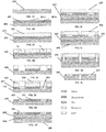
Figure 3 depicts a cross-sectional view of a moon-phase display component for a watch at various stages of fabrication in accordance with embodiments of the present invention; and -
Figure 4 depicts a functional block diagram of an apparatus for fabricating the moon-phase display component for a watch not forming part of the present invention, the moon-phase display including multiple colour characteristics. - Embodiments of the present invention will now be described with reference to
Figs. 1 to 4 . - Referring firstly to
Fig. 2 , a method is provided in accordance with embodiments of the present invention for use in fabricating a watch component (1) as shown inFig. 1 having multiple colour characteristics. By way of example, the watch component (1) fabricated in accordance with these embodiments includes a moon-phase display having a blue coloured background (11), and gold coloured moon (12) and stars (13) pattern. It should be understood that other types of watch components with other types of colour characteristics may of course also be fabricated using this apparatus. - As shown in
Fig. 4 , the apparatus includes a computerised controller (400) having an input and output user interface which is configured for controlling a thin film deposition apparatus (404), a photolithography apparatus (403), a sputtering apparatus (402) and an etching apparatus (401). - An opaque silicon wafer (300) is used to form the base of the moon-phase display (1) as shown in
Fig. 3A . A first thin film of silicon nitride (301) is deposited on to the silicon wafer (300) as shown inFig. 3B with the first thin film (301) having a thickness in the sub-nanometer to micron range so as to reflect certain wavelengths of light. This step is represented by block (201) inFig. 2 . Before the first thin film (301) is deposited on the silicon wafer (300) by the thin film deposition apparatus (404), the silicon wafer (300) is thoroughly cleaned (e.g. in accordance with "RCA" standardised procedure) to remove small particles on the silicon surface which may give rise to defects in the first thin film (301). - In an example, the apparatus is configured to deposit the first thin film (301) of silicon nitride on to the silicon wafer (300) using a plasma-enhanced chemical vapour deposition (PECVD) process or a low pressure chemical vapour deposition (LPCVD) process. PECVD and LPCVD processes are suitable for use in producing ultra thin film with high refractive index whereby the reflected light exhibits good monochromatic properties.
- As light strikes the first thin film (301), it is both transmitted and reflected at the upper surface of (301a) the first thin film (301). The light transmitted through the upper surface (301a) reaches the lower surface (301b) interfaced with the silicon wafer (300) and is reflected away from the silicon wafer (300) with the light reflected away from the upper (301a) and lower surfaces (301b) undergoing interference. For a given first thin film (301) with a reflective index of n, a film thickness of d, the reflected wavelength is governed by the equation of mλ=2ndCosθ where m is the order of the interfered light, λ is the wavelength of the reflected light, and θ is the incident angle inside the first thin film (301). The blue background of the moon-phase display (1) can thus be fabricated by depositing the first thin film (301) to a thickness (typically around about 937.5 Å) in accordance with the above equation and parameters which reflects light indicative of blue as perceived by the human eye.
- The gases used in the preferred examples for growing of silicon nitride (301) by PECVD includes silane, ammonia, and nitrogen. The deposition rate of the silicon nitride first thin film (301) can be controlled by the flow rate of these gases, the RF power, the deposition pressure and other parameters. In order to have good control of the thin film thickness, a relatively low growth rate is preferable. The PECVD machine used in embodiments of the present invention includes an Oxford Plasma 80 machine providing a controlled growth rate of approximately 23nm/min. By changing the deposition time, the thin film thickness can be tightly controlled, and in turn, the wavelength of the reflected light and perceived colour of the thin film may similarly be tightly controlled. LPCVD has an even slower growth rate, which results in a relatively dense film.
- The apparatus is also configured to fabricate a second colour characteristic in the form of a gold colour patterned moon (12) and stars (13) on the moon phase display.
- During the fabrication, two masks are needed. The first mask is for patterning the silicon wafer with the moon (12) and stars (13), the second one is for etching through the wafer and releasing the moon phase displays from the wafer.
- The photoresist mask (302) is coated on to the first thin film (301) of the silicon wafer (300) by the photolithography apparatus (403) and baked as shown in
Fig. 3C . This step is represented by block (202) inFig 2 . For high resolution photolithography a positive photoresist mask (302) such as AZ 5214E is normally used. The photoresist (302) is spin-coated on to the first thin film (301) of the silicon wafer (300) at a speed of 4000 RPM which results in a thickness of about 1.4µm. - After baking, the photoresist (302) coated silicon wafer (300) is then exposed under UV light by the photolithography apparatus (403) which causes a chemical change in specific regions of the photoresist mask (302) corresponding to the moon (12) and stars (13) patterns (shown in
Fig. 3D ) that can thereafter be removed from the photoresist (302) by developer such asAZ 300 MIF before being baked again. The baking assists in enhancing the adhesion between the photoresist (302) and the silicon wafer (300) so as to avoid defects arising in the following steps. The thin positive photoresist mask (302) assists in defining a relatively sharper and more precise boundary of the moon (12) and stars (13) patterns which subsequently results in sharper transfer of the moon (12) and stars (13) patterns on to the silicon wafer (300). - The silicon wafer (300) is next ready for etching in HF solution whereby the silicon under the moon (12) and stars (13) patterns is exposed when the silicon nitride (301) within boundaries of the patterns not covered by the photoresist (302) are etched away by HF as shown in
Fig. 3E . The etching time of this step is of importance because over-etching of silicon nitride (301) will adversely affect the quality of the resulting moons (12) and stars (13) patterns. After cleaning in deionised water, the silicon wafer (300) is blown dry with nitrogen. - Thereafter, gold particles are sputtered on to the exposed silicon within the boundaries of the moon (12) and stars (13) patterns using the sputtering apparatus (402) which could for instance be either a magnetron sputtering deposition apparatus or electron-beam evaporation deposition apparatus. In seeking to enhance the amount of adhesion between the sputtered gold particles and the silicon surface a thin layer (approximately less than 50nm) of chromium or titanium is deposited on to the exposed silicon before sputtering gold as shown in
Fig. 3F . The thickness of the sputtered gold within the boundaries of the moon (12) and stars (13) patters is about 100nm. In alternative embodiments, other metals or ceramic particles may be sputtered on to the silicon wafer (300). This step is represented generally by blocks (203), (205) and (206) inFig. 2 . - Referring to
Fig, 3G , the silicon wafer (300) is then immersed into acetone to remove the remaining photoresist mask (302) whereby the gold on the photoresist (302) will be washed away together with the photoresist (302), leaving the silicon wafer (300) covered with gold only in the area of the moon (12) and stars (13) patterns. - Thereafter, the silicon wafer (300) is bonded to a handle wafer (305) with wax (304) as shown in
Fig. 3H . This step is desirable as the silicon wafer (300) with the moon (12) and stars (13) patterns is to be etched through using the etching apparatus (401). During the etching process, the backside of the silicon wafer (300) is cooled with helium which is blown towards the back of the silicon wafer (300). If the silicon wafer (300) is not bonded to a handle wafer (305), helium will blow into the process chamber when the silicon wafer (300) is partially etched through thus affecting the process. At the same time, there is risk of leaving broken silicon within the chamber. - After the wafer bonding step is completed, another layer of photoresist (306) is coated on the silicon wafer (300) for a second lithography as shown in
Fig. 3I . In this step, the counter lines of the moon phase display are defined. In order to provide a photoresist (306) of suitable thickness for the etching through process whilst at the same time maintaining high enough accuracy, an AZ P4620 positive photoresist (306) is used. - In this photolithography process, as shown in
Fig. 3J , the photoresist (306) is aligned with the marks on the wafer generated by the first mask (302), so as to expose the counter line of the moon phase display. Before the next step, the silicon wafer (300) covered with photoresist (306) is baked again. - Referring now to
Fig. 3K , although the exposed area is still covered with silicon nitride, the silicon wafer can be transferred to a DRIE machine for etching through with a Bosch process. Advantageously, the gas for etching silicon in the Bosch process is SF6 can also etch silicon nitride such that there is no need to remove the silicon nitride layer before etching the silicon. This is one reason for choosing to use silicon nitride in the first thin film to produce the first colour characteristic of the moon-phase display. - Referring to
Fig. 3L , when the silicon wafer (300) is fully etched through in the DRIE machine, the moon phase display (1) is ready to be released from the handle wafer (305) in acetone or other solvent needed by for removing the bonding wax (304). After proper cleaning, the moon phase display (1) is ready to be used. - In alternative embodiments, the second colour characteristic of the gold coloured moon (12) and stars (13) is produced by depositing a second thin film of silicon nitride within the boundaries of the moon (12) and stars (13) patterns defined by the photoresist mask (302) instead of sputtering gold particles thereon. The deposition of the second thin film is achieved using a PECVD process. This step is represented by
step 204 inFig. 2 . - Silicon nitride within the first regions defining the moon (12) and stars (13) patterns can be at least partially removed (e.g. using HF or dry etching) before the second thin film of silicon nitride is deposited therein to a thickness suitable for producing the gold colour. For instance, a gold colour of suitable quality for high-end watch applications may typically require a thickness of around 169nm. This step is represented by blocks (207) and (210) in
Fig. 2 . - In yet alternative embodiments of the present invention, the method may be configured to produce the gold colour by depositing a second thin film within boundaries of the moon (12) and stars (13) patterns defined by the photoresist mask (302) without removing any of the first thin film within the moon (12) and stars (13) pattern boundaries such that the combined thickness of the second thin film and the first thin film are of a suitable thickness to produce the second colour characteristic. This step is represented by block (209) in
Fig. 2 . - Yet alternatively, the apparatus for processing the first region to produce the second colour characteristic is configured to thin the first thin film to a desired thickness suitable for producing the second colour characteristic. The thinning can be achieved for instance by HF solution or dry etching. This step is represented by block (208) in
Fig. 2 . - It should be noted that a first thin film deposited by LPCVD is relatively difficult to be etched with HF (hydrogen fluoride) solution, and is suited to being etched using a dry etching method. The process temperature of LPCVD is high (i.e. normally up to around 700°) which is too high for a photoresist used in the photolithography step and restricts flexibility in the design process. For this reason LPCVD is generally unsuitable for generating the second colour characteristic. It is however suitable for producing the first colour characteristic where only bare silicon wafer is used.
- After the second colour is fabricated, another photolithography step can be performed as represented by blocks (211) and (212) in
Fig 2 if a third colour is needed. If two colours are enough for the application, the photolithography step is to expose the boundary area for releasing etch as represented by block (213) inFig. 2 . After the releasing etch by DRIE as represented by block (213) inFig. 2 , the whole silicon wafer is immerged in acetone or other solvent for component releasing as represented by block (214) inFig. 2 . - Illustratively, other components for use in a watch may be formed including for instance a silicon escape wheel, a silicon pallet fork, a silicon bridge, a silicon hour/minute/seconds hand and a silicon dial.
- In yet other examples, components may be formed for decorative purposes applicable to devices other than watches including displays for electronic devices, jewellery and so on.
Claims (10)
- A method of fabricating a component for use in a watch, including a step of depositing a first thin film on a wafer wherein the first thin film is adapted to allow light reflected away from the wafer to be indicative of a first colour characteristic, and a further step of fabricating a second colour characteristic on the wafer, the further step including defining a pattern on the first thin film, and, processing a region within a boundary of the pattern so that the region is adapted to be indicative of the second colour characteristic, the step of processing the region within the boundary of the pattern includes at least one of:(a) depositing a metal material within the boundary of the pattern which is indicative of the second colour characteristic;(b) removing at least some of the first thin film within the boundary of the pattern and thereafter depositing a second thin film therein wherein the second thin film is adapted to produce the second colour characteristic; and(c) depositing a second thin film within the region within the boundary of the pattern without removing any of the first thin film within the boundary of the pattern such that the second thin film either alone or in combination with the first thin film is adapted to produce the second colour characteristic; and(d) wherein, the method is characterised in that the step of defining the pattern on the first thin film is performed using photolithography.
- A method as claimed in claim 1 wherein the wafer includes an opaque material.
- A method as claimed in claims 1 or 2 wherein the wafer includes a silicon wafer.
- A method as claimed in any one of the preceding claims where in the step of depositing the first thin film on the wafer is performed using at least one of a plasma-enhanced chemical vapour deposition process and a low pressure chemical vapour deposition process.
- A method as claimed in any one of the preceding claims wherein the first thin film includes a refractive index greater than 2.
- A method as claimed in any one of the preceding claims wherein the pattern includes a moon or a star shape.
- A method as claimed in any preceding claim, wherein the metal material is deposited within the boundary of the pattern using at least one of a magnetron sputtering deposition process and an electron-beam evaporation deposition process.
- A method as claimed in any one of the preceding claims wherein the second thin film is deposited using a plasma-enhanced chemical vapour deposition process.
- A method as claimed in any one of the preceding claims wherein the step of processing the region within the boundary of the pattern includes thinning the first thin film within the boundary of the pattern to a thickness suitable for producing the second colour characteristic.
- A method as claimed in claim 9 wherein at least one of the first thin film and the second thin film include a silicon nitride material.
Applications Claiming Priority (1)
| Application Number | Priority Date | Filing Date | Title |
|---|---|---|---|
| HK13105967.3A HK1190568A2 (en) | 2013-05-21 | 2013-05-21 | A method and apparatus for frabricating a coloured component for a watch |
Publications (3)
| Publication Number | Publication Date |
|---|---|
| EP2806315A2 EP2806315A2 (en) | 2014-11-26 |
| EP2806315A3 EP2806315A3 (en) | 2016-04-13 |
| EP2806315B1 true EP2806315B1 (en) | 2019-02-13 |
Family
ID=51022684
Family Applications (1)
| Application Number | Title | Priority Date | Filing Date |
|---|---|---|---|
| EP14169164.2A Not-in-force EP2806315B1 (en) | 2013-05-21 | 2014-05-20 | A method for fabricating a coloured component for a watch |
Country Status (4)
| Country | Link |
|---|---|
| US (1) | US9625879B2 (en) |
| EP (1) | EP2806315B1 (en) |
| CN (1) | CN104181801B (en) |
| HK (1) | HK1190568A2 (en) |
Families Citing this family (11)
| Publication number | Priority date | Publication date | Assignee | Title |
|---|---|---|---|---|
| EP3035129B1 (en) * | 2014-12-19 | 2020-11-04 | The Swatch Group Research and Development Ltd | Method for producing a decorated element of a timepiece or piece of jewellery |
| EP3035130B1 (en) * | 2014-12-19 | 2022-03-02 | Omega SA | Method for producing a decorated element of a timepiece or piece of jewellery, and element produced by the method |
| HK1213429A2 (en) * | 2015-12-31 | 2016-06-30 | Master Dynamic Limited | Method of forming a marking on an article, and an article having a mark thereon |
| JP1569778S (en) * | 2016-01-29 | 2017-02-20 | ||
| CN108258068A (en) * | 2018-01-31 | 2018-07-06 | 北京铂阳顶荣光伏科技有限公司 | Colored solar battery and preparation method thereof |
| TWI774925B (en) * | 2018-03-01 | 2022-08-21 | 瑞士商Csem瑞士電子及微技術研發公司 | Method for manufacturing a spiral spring |
| JP6908064B2 (en) | 2019-03-14 | 2021-07-21 | セイコーエプソン株式会社 | Watch parts, watch movements and watches |
| JP7238657B2 (en) * | 2019-07-16 | 2023-03-14 | セイコーエプソン株式会社 | Watch parts, watch movements and watches |
| JP7613027B2 (en) * | 2020-09-08 | 2025-01-15 | セイコーエプソン株式会社 | Clock dial, method of manufacturing clock dial, and clock |
| EP4206826B1 (en) * | 2021-12-30 | 2026-04-29 | Rubattel et Weyermann S.A. | Method for manufacturing brackets on a dial |
| JP2023140590A (en) * | 2022-03-23 | 2023-10-05 | セイコーエプソン株式会社 | Watch parts, watch movements and watches |
Family Cites Families (14)
| Publication number | Priority date | Publication date | Assignee | Title |
|---|---|---|---|---|
| FR2547775B1 (en) * | 1983-06-23 | 1987-12-18 | Metalem Sa | METHOD FOR DECORATING AN ARTICLE, APPLICATION OF A PROCESS FOR TREATING A SILICON ELEMENT, USE OF A TREATED SILICON PLATE AND DECORATED ARTICLE |
| EP0220716B1 (en) * | 1985-10-29 | 1994-06-01 | Andreas Biedermann | Decorated article |
| DE3635567C2 (en) * | 1985-10-29 | 1993-10-14 | Andreas Biedermann | Decorated item |
| EP0399072B1 (en) * | 1989-05-23 | 1992-12-09 | BOCK & SCHUPP GMBH & CO. KG | Piece of jewellery |
| US5639671A (en) * | 1989-09-18 | 1997-06-17 | Biostar, Inc. | Methods for optimizing of an optical assay device |
| US5888593A (en) * | 1994-03-03 | 1999-03-30 | Monsanto Company | Ion beam process for deposition of highly wear-resistant optical coatings |
| US6103572A (en) * | 1997-02-07 | 2000-08-15 | Citizen Watch Co., Ltd. | Method of fabricating a semiconductor nonvolatile storage device |
| JP2006029866A (en) | 2004-07-13 | 2006-02-02 | Seiko Epson Corp | Timepiece parts manufacturing method, timepiece parts, timepiece |
| US7382515B2 (en) * | 2006-01-18 | 2008-06-03 | Qualcomm Mems Technologies, Inc. | Silicon-rich silicon nitrides as etch stops in MEMS manufacture |
| EP1998602B1 (en) * | 2007-03-29 | 2014-03-05 | Alpha Metals, Inc. | Method of manufacturing electrical contacts |
| JP2009135223A (en) * | 2007-11-29 | 2009-06-18 | Oki Semiconductor Co Ltd | Semiconductor device and manufacturing method thereof |
| JP5326407B2 (en) * | 2008-07-31 | 2013-10-30 | セイコーエプソン株式会社 | Watch cover glass and watch |
| JP2010216898A (en) | 2009-03-13 | 2010-09-30 | Seiko Epson Corp | Method for manufacturing dial for timepiece, dial for timepiece, and timepiece |
| TWI469365B (en) * | 2009-04-01 | 2015-01-11 | Gintech Energy Corp | High-efficiency color solar cell and method of manufacturing same |
-
2013
- 2013-05-21 HK HK13105967.3A patent/HK1190568A2/en not_active IP Right Cessation
-
2014
- 2014-05-20 EP EP14169164.2A patent/EP2806315B1/en not_active Not-in-force
- 2014-05-21 US US14/283,928 patent/US9625879B2/en not_active Expired - Fee Related
- 2014-05-21 CN CN201410217105.2A patent/CN104181801B/en not_active Expired - Fee Related
Non-Patent Citations (1)
| Title |
|---|
| None * |
Also Published As
| Publication number | Publication date |
|---|---|
| CN104181801A (en) | 2014-12-03 |
| HK1204372A1 (en) | 2015-11-13 |
| HK1204371A1 (en) | 2015-11-13 |
| EP2806315A2 (en) | 2014-11-26 |
| EP2806315A3 (en) | 2016-04-13 |
| US20140356638A1 (en) | 2014-12-04 |
| HK1190568A2 (en) | 2014-07-04 |
| CN104181801B (en) | 2018-05-04 |
| US9625879B2 (en) | 2017-04-18 |
Similar Documents
| Publication | Publication Date | Title |
|---|---|---|
| US9625879B2 (en) | Method for fabricating a colored component for a watch | |
| CN110268337B (en) | Clock dials or external elements made of non-conductive materials | |
| KR102523685B1 (en) | External element or dial for horology or jewellery made of conductive material | |
| US20150092524A1 (en) | Ceramic element inlaid with at least one ceramic decoration | |
| EP3035128A1 (en) | Method for producing a decorated component of a timepiece or piece of jewellery, and component produced by the method | |
| CN116027652B (en) | Method for decorating a substrate | |
| JP2020148651A (en) | Component for watch, movement for watch, and watch | |
| HK1204372B (en) | A method for fabricating a coloured component for a watch | |
| CH715925A2 (en) | Cladding element or watch or jewelery dial in conductive material. | |
| US20240036522A1 (en) | Method for manufacturing a horological component | |
| JP7842708B2 (en) | Exterior components for watches or jewelry and methods for manufacturing such exterior components | |
| CN117724197A (en) | Method for manufacturing exterior part comprising diffraction grating | |
| HK1204371B (en) | A method and apparatus for fabricating a coloured component for a watch | |
| HK40121608A (en) | External element or dial for horology or jewellery made of conductive material | |
| JP7793569B2 (en) | Decorative member for watch and manufacturing method thereof | |
| HK40014674A (en) | Timepiece dial or covering element made from non-conductive material | |
| HK40014674B (en) | Timepiece dial or covering element made from non-conductive material | |
| TWI869838B (en) | Method for manufacturing a silicon balance spring | |
| HK40037459A (en) | External element or dial for horology or jewellery made of conductive material | |
| HK40091150A (en) | External component of a watch or of an item of jewellery and method for manufacturing such an external component | |
| HK40106851A (en) | Method for manufacturing a silicon balance spring | |
| JP2023099302A (en) | How to make decorations on the dial |
Legal Events
| Date | Code | Title | Description |
|---|---|---|---|
| PUAI | Public reference made under article 153(3) epc to a published international application that has entered the european phase |
Free format text: ORIGINAL CODE: 0009012 |
|
| 17P | Request for examination filed |
Effective date: 20140520 |
|
| AK | Designated contracting states |
Kind code of ref document: A2 Designated state(s): AL AT BE BG CH CY CZ DE DK EE ES FI FR GB GR HR HU IE IS IT LI LT LU LV MC MK MT NL NO PL PT RO RS SE SI SK SM TR |
|
| AX | Request for extension of the european patent |
Extension state: BA ME |
|
| REG | Reference to a national code |
Ref country code: HK Ref legal event code: DE Ref document number: 1204372 Country of ref document: HK |
|
| PUAL | Search report despatched |
Free format text: ORIGINAL CODE: 0009013 |
|
| AK | Designated contracting states |
Kind code of ref document: A3 Designated state(s): AL AT BE BG CH CY CZ DE DK EE ES FI FR GB GR HR HU IE IS IT LI LT LU LV MC MK MT NL NO PL PT RO RS SE SI SK SM TR |
|
| AX | Request for extension of the european patent |
Extension state: BA ME |
|
| RIC1 | Information provided on ipc code assigned before grant |
Ipc: G04B 19/12 20060101ALI20160308BHEP Ipc: G04D 3/00 20060101AFI20160308BHEP |
|
| R17P | Request for examination filed (corrected) |
Effective date: 20161012 |
|
| RBV | Designated contracting states (corrected) |
Designated state(s): AL AT BE BG CH CY CZ DE DK EE ES FI FR GB GR HR HU IE IS IT LI LT LU LV MC MK MT NL NO PL PT RO RS SE SI SK SM TR |
|
| STAA | Information on the status of an ep patent application or granted ep patent |
Free format text: STATUS: REQUEST FOR EXAMINATION WAS MADE |
|
| R17P | Request for examination filed (corrected) |
Effective date: 20161012 |
|
| STAA | Information on the status of an ep patent application or granted ep patent |
Free format text: STATUS: EXAMINATION IS IN PROGRESS |
|
| 17Q | First examination report despatched |
Effective date: 20170707 |
|
| GRAP | Despatch of communication of intention to grant a patent |
Free format text: ORIGINAL CODE: EPIDOSNIGR1 |
|
| STAA | Information on the status of an ep patent application or granted ep patent |
Free format text: STATUS: GRANT OF PATENT IS INTENDED |
|
| INTG | Intention to grant announced |
Effective date: 20181017 |
|
| GRAJ | Information related to disapproval of communication of intention to grant by the applicant or resumption of examination proceedings by the epo deleted |
Free format text: ORIGINAL CODE: EPIDOSDIGR1 |
|
| STAA | Information on the status of an ep patent application or granted ep patent |
Free format text: STATUS: EXAMINATION IS IN PROGRESS |
|
| GRAR | Information related to intention to grant a patent recorded |
Free format text: ORIGINAL CODE: EPIDOSNIGR71 |
|
| GRAS | Grant fee paid |
Free format text: ORIGINAL CODE: EPIDOSNIGR3 |
|
| STAA | Information on the status of an ep patent application or granted ep patent |
Free format text: STATUS: GRANT OF PATENT IS INTENDED |
|
| INTC | Intention to grant announced (deleted) | ||
| GRAA | (expected) grant |
Free format text: ORIGINAL CODE: 0009210 |
|
| STAA | Information on the status of an ep patent application or granted ep patent |
Free format text: STATUS: THE PATENT HAS BEEN GRANTED |
|
| INTG | Intention to grant announced |
Effective date: 20190103 |
|
| AK | Designated contracting states |
Kind code of ref document: B1 Designated state(s): AL AT BE BG CH CY CZ DE DK EE ES FI FR GB GR HR HU IE IS IT LI LT LU LV MC MK MT NL NO PL PT RO RS SE SI SK SM TR |
|
| REG | Reference to a national code |
Ref country code: GB Ref legal event code: FG4D |
|
| REG | Reference to a national code |
Ref country code: CH Ref legal event code: EP Ref country code: AT Ref legal event code: REF Ref document number: 1096576 Country of ref document: AT Kind code of ref document: T Effective date: 20190215 |
|
| REG | Reference to a national code |
Ref country code: IE Ref legal event code: FG4D |
|
| REG | Reference to a national code |
Ref country code: DE Ref legal event code: R096 Ref document number: 602014040933 Country of ref document: DE |
|
| PGFP | Annual fee paid to national office [announced via postgrant information from national office to epo] |
Ref country code: GB Payment date: 20190307 Year of fee payment: 6 |
|
| RAP2 | Party data changed (patent owner data changed or rights of a patent transferred) |
Owner name: MASTER DYNAMIC LIMITED |
|
| REG | Reference to a national code |
Ref country code: LT Ref legal event code: MG4D |
|
| REG | Reference to a national code |
Ref country code: NL Ref legal event code: MP Effective date: 20190213 |
|
| PG25 | Lapsed in a contracting state [announced via postgrant information from national office to epo] |
Ref country code: PT Free format text: LAPSE BECAUSE OF FAILURE TO SUBMIT A TRANSLATION OF THE DESCRIPTION OR TO PAY THE FEE WITHIN THE PRESCRIBED TIME-LIMIT Effective date: 20190613 Ref country code: SE Free format text: LAPSE BECAUSE OF FAILURE TO SUBMIT A TRANSLATION OF THE DESCRIPTION OR TO PAY THE FEE WITHIN THE PRESCRIBED TIME-LIMIT Effective date: 20190213 Ref country code: FI Free format text: LAPSE BECAUSE OF FAILURE TO SUBMIT A TRANSLATION OF THE DESCRIPTION OR TO PAY THE FEE WITHIN THE PRESCRIBED TIME-LIMIT Effective date: 20190213 Ref country code: LT Free format text: LAPSE BECAUSE OF FAILURE TO SUBMIT A TRANSLATION OF THE DESCRIPTION OR TO PAY THE FEE WITHIN THE PRESCRIBED TIME-LIMIT Effective date: 20190213 Ref country code: NO Free format text: LAPSE BECAUSE OF FAILURE TO SUBMIT A TRANSLATION OF THE DESCRIPTION OR TO PAY THE FEE WITHIN THE PRESCRIBED TIME-LIMIT Effective date: 20190513 Ref country code: NL Free format text: LAPSE BECAUSE OF FAILURE TO SUBMIT A TRANSLATION OF THE DESCRIPTION OR TO PAY THE FEE WITHIN THE PRESCRIBED TIME-LIMIT Effective date: 20190213 |
|
| PGFP | Annual fee paid to national office [announced via postgrant information from national office to epo] |
Ref country code: DE Payment date: 20190513 Year of fee payment: 6 |
|
| PG25 | Lapsed in a contracting state [announced via postgrant information from national office to epo] |
Ref country code: GR Free format text: LAPSE BECAUSE OF FAILURE TO SUBMIT A TRANSLATION OF THE DESCRIPTION OR TO PAY THE FEE WITHIN THE PRESCRIBED TIME-LIMIT Effective date: 20190514 Ref country code: IS Free format text: LAPSE BECAUSE OF FAILURE TO SUBMIT A TRANSLATION OF THE DESCRIPTION OR TO PAY THE FEE WITHIN THE PRESCRIBED TIME-LIMIT Effective date: 20190613 Ref country code: HR Free format text: LAPSE BECAUSE OF FAILURE TO SUBMIT A TRANSLATION OF THE DESCRIPTION OR TO PAY THE FEE WITHIN THE PRESCRIBED TIME-LIMIT Effective date: 20190213 Ref country code: LV Free format text: LAPSE BECAUSE OF FAILURE TO SUBMIT A TRANSLATION OF THE DESCRIPTION OR TO PAY THE FEE WITHIN THE PRESCRIBED TIME-LIMIT Effective date: 20190213 Ref country code: BG Free format text: LAPSE BECAUSE OF FAILURE TO SUBMIT A TRANSLATION OF THE DESCRIPTION OR TO PAY THE FEE WITHIN THE PRESCRIBED TIME-LIMIT Effective date: 20190513 Ref country code: RS Free format text: LAPSE BECAUSE OF FAILURE TO SUBMIT A TRANSLATION OF THE DESCRIPTION OR TO PAY THE FEE WITHIN THE PRESCRIBED TIME-LIMIT Effective date: 20190213 |
|
| PGFP | Annual fee paid to national office [announced via postgrant information from national office to epo] |
Ref country code: FR Payment date: 20190509 Year of fee payment: 6 |
|
| REG | Reference to a national code |
Ref country code: AT Ref legal event code: MK05 Ref document number: 1096576 Country of ref document: AT Kind code of ref document: T Effective date: 20190213 |
|
| PGFP | Annual fee paid to national office [announced via postgrant information from national office to epo] |
Ref country code: CH Payment date: 20190514 Year of fee payment: 6 |
|
| PG25 | Lapsed in a contracting state [announced via postgrant information from national office to epo] |
Ref country code: IT Free format text: LAPSE BECAUSE OF FAILURE TO SUBMIT A TRANSLATION OF THE DESCRIPTION OR TO PAY THE FEE WITHIN THE PRESCRIBED TIME-LIMIT Effective date: 20190213 Ref country code: CZ Free format text: LAPSE BECAUSE OF FAILURE TO SUBMIT A TRANSLATION OF THE DESCRIPTION OR TO PAY THE FEE WITHIN THE PRESCRIBED TIME-LIMIT Effective date: 20190213 Ref country code: EE Free format text: LAPSE BECAUSE OF FAILURE TO SUBMIT A TRANSLATION OF THE DESCRIPTION OR TO PAY THE FEE WITHIN THE PRESCRIBED TIME-LIMIT Effective date: 20190213 Ref country code: RO Free format text: LAPSE BECAUSE OF FAILURE TO SUBMIT A TRANSLATION OF THE DESCRIPTION OR TO PAY THE FEE WITHIN THE PRESCRIBED TIME-LIMIT Effective date: 20190213 Ref country code: ES Free format text: LAPSE BECAUSE OF FAILURE TO SUBMIT A TRANSLATION OF THE DESCRIPTION OR TO PAY THE FEE WITHIN THE PRESCRIBED TIME-LIMIT Effective date: 20190213 Ref country code: DK Free format text: LAPSE BECAUSE OF FAILURE TO SUBMIT A TRANSLATION OF THE DESCRIPTION OR TO PAY THE FEE WITHIN THE PRESCRIBED TIME-LIMIT Effective date: 20190213 Ref country code: AL Free format text: LAPSE BECAUSE OF FAILURE TO SUBMIT A TRANSLATION OF THE DESCRIPTION OR TO PAY THE FEE WITHIN THE PRESCRIBED TIME-LIMIT Effective date: 20190213 Ref country code: SK Free format text: LAPSE BECAUSE OF FAILURE TO SUBMIT A TRANSLATION OF THE DESCRIPTION OR TO PAY THE FEE WITHIN THE PRESCRIBED TIME-LIMIT Effective date: 20190213 |
|
| REG | Reference to a national code |
Ref country code: DE Ref legal event code: R097 Ref document number: 602014040933 Country of ref document: DE |
|
| PG25 | Lapsed in a contracting state [announced via postgrant information from national office to epo] |
Ref country code: PL Free format text: LAPSE BECAUSE OF FAILURE TO SUBMIT A TRANSLATION OF THE DESCRIPTION OR TO PAY THE FEE WITHIN THE PRESCRIBED TIME-LIMIT Effective date: 20190213 Ref country code: SM Free format text: LAPSE BECAUSE OF FAILURE TO SUBMIT A TRANSLATION OF THE DESCRIPTION OR TO PAY THE FEE WITHIN THE PRESCRIBED TIME-LIMIT Effective date: 20190213 |
|
| PLBE | No opposition filed within time limit |
Free format text: ORIGINAL CODE: 0009261 |
|
| STAA | Information on the status of an ep patent application or granted ep patent |
Free format text: STATUS: NO OPPOSITION FILED WITHIN TIME LIMIT |
|
| PG25 | Lapsed in a contracting state [announced via postgrant information from national office to epo] |
Ref country code: AT Free format text: LAPSE BECAUSE OF FAILURE TO SUBMIT A TRANSLATION OF THE DESCRIPTION OR TO PAY THE FEE WITHIN THE PRESCRIBED TIME-LIMIT Effective date: 20190213 |
|
| 26N | No opposition filed |
Effective date: 20191114 |
|
| PG25 | Lapsed in a contracting state [announced via postgrant information from national office to epo] |
Ref country code: MC Free format text: LAPSE BECAUSE OF FAILURE TO SUBMIT A TRANSLATION OF THE DESCRIPTION OR TO PAY THE FEE WITHIN THE PRESCRIBED TIME-LIMIT Effective date: 20190213 |
|
| REG | Reference to a national code |
Ref country code: BE Ref legal event code: MM Effective date: 20190531 |
|
| PG25 | Lapsed in a contracting state [announced via postgrant information from national office to epo] |
Ref country code: SI Free format text: LAPSE BECAUSE OF FAILURE TO SUBMIT A TRANSLATION OF THE DESCRIPTION OR TO PAY THE FEE WITHIN THE PRESCRIBED TIME-LIMIT Effective date: 20190213 Ref country code: LU Free format text: LAPSE BECAUSE OF NON-PAYMENT OF DUE FEES Effective date: 20190520 |
|
| PG25 | Lapsed in a contracting state [announced via postgrant information from national office to epo] |
Ref country code: TR Free format text: LAPSE BECAUSE OF FAILURE TO SUBMIT A TRANSLATION OF THE DESCRIPTION OR TO PAY THE FEE WITHIN THE PRESCRIBED TIME-LIMIT Effective date: 20190213 |
|
| PG25 | Lapsed in a contracting state [announced via postgrant information from national office to epo] |
Ref country code: IE Free format text: LAPSE BECAUSE OF NON-PAYMENT OF DUE FEES Effective date: 20190520 |
|
| PG25 | Lapsed in a contracting state [announced via postgrant information from national office to epo] |
Ref country code: BE Free format text: LAPSE BECAUSE OF NON-PAYMENT OF DUE FEES Effective date: 20190531 |
|
| REG | Reference to a national code |
Ref country code: DE Ref legal event code: R119 Ref document number: 602014040933 Country of ref document: DE |
|
| PG25 | Lapsed in a contracting state [announced via postgrant information from national office to epo] |
Ref country code: LI Free format text: LAPSE BECAUSE OF NON-PAYMENT OF DUE FEES Effective date: 20200531 Ref country code: CH Free format text: LAPSE BECAUSE OF NON-PAYMENT OF DUE FEES Effective date: 20200531 |
|
| GBPC | Gb: european patent ceased through non-payment of renewal fee |
Effective date: 20200520 |
|
| PG25 | Lapsed in a contracting state [announced via postgrant information from national office to epo] |
Ref country code: GB Free format text: LAPSE BECAUSE OF NON-PAYMENT OF DUE FEES Effective date: 20200520 Ref country code: FR Free format text: LAPSE BECAUSE OF NON-PAYMENT OF DUE FEES Effective date: 20200531 |
|
| PG25 | Lapsed in a contracting state [announced via postgrant information from national office to epo] |
Ref country code: CY Free format text: LAPSE BECAUSE OF FAILURE TO SUBMIT A TRANSLATION OF THE DESCRIPTION OR TO PAY THE FEE WITHIN THE PRESCRIBED TIME-LIMIT Effective date: 20190213 Ref country code: DE Free format text: LAPSE BECAUSE OF NON-PAYMENT OF DUE FEES Effective date: 20201201 |
|
| PG25 | Lapsed in a contracting state [announced via postgrant information from national office to epo] |
Ref country code: MT Free format text: LAPSE BECAUSE OF FAILURE TO SUBMIT A TRANSLATION OF THE DESCRIPTION OR TO PAY THE FEE WITHIN THE PRESCRIBED TIME-LIMIT Effective date: 20190213 Ref country code: HU Free format text: LAPSE BECAUSE OF FAILURE TO SUBMIT A TRANSLATION OF THE DESCRIPTION OR TO PAY THE FEE WITHIN THE PRESCRIBED TIME-LIMIT; INVALID AB INITIO Effective date: 20140520 |
|
| PG25 | Lapsed in a contracting state [announced via postgrant information from national office to epo] |
Ref country code: MK Free format text: LAPSE BECAUSE OF FAILURE TO SUBMIT A TRANSLATION OF THE DESCRIPTION OR TO PAY THE FEE WITHIN THE PRESCRIBED TIME-LIMIT Effective date: 20190213 |