EP2804442B1 - Power supply device, method for managing power supply thereof and wireless communication terminal - Google Patents
Power supply device, method for managing power supply thereof and wireless communication terminal Download PDFInfo
- Publication number
- EP2804442B1 EP2804442B1 EP12864832.6A EP12864832A EP2804442B1 EP 2804442 B1 EP2804442 B1 EP 2804442B1 EP 12864832 A EP12864832 A EP 12864832A EP 2804442 B1 EP2804442 B1 EP 2804442B1
- Authority
- EP
- European Patent Office
- Prior art keywords
- power supply
- power
- unit
- cpu
- supply device
- Prior art date
- Legal status (The legal status is an assumption and is not a legal conclusion. Google has not performed a legal analysis and makes no representation as to the accuracy of the status listed.)
- Active
Links
Images



Classifications
-
- H—ELECTRICITY
- H02—GENERATION; CONVERSION OR DISTRIBUTION OF ELECTRIC POWER
- H02M—APPARATUS FOR CONVERSION BETWEEN AC AND AC, BETWEEN AC AND DC, OR BETWEEN DC AND DC, AND FOR USE WITH MAINS OR SIMILAR POWER SUPPLY SYSTEMS; CONVERSION OF DC OR AC INPUT POWER INTO SURGE OUTPUT POWER; CONTROL OR REGULATION THEREOF
- H02M3/00—Conversion of DC power input into DC power output
- H02M3/02—Conversion of DC power input into DC power output without intermediate conversion into AC
- H02M3/04—Conversion of DC power input into DC power output without intermediate conversion into AC by static converters
- H02M3/10—Conversion of DC power input into DC power output without intermediate conversion into AC by static converters using discharge tubes with control electrode or semiconductor devices with control electrode
- H02M3/145—Conversion of DC power input into DC power output without intermediate conversion into AC by static converters using discharge tubes with control electrode or semiconductor devices with control electrode using devices of a triode or transistor type requiring continuous application of a control signal
- H02M3/155—Conversion of DC power input into DC power output without intermediate conversion into AC by static converters using discharge tubes with control electrode or semiconductor devices with control electrode using devices of a triode or transistor type requiring continuous application of a control signal using semiconductor devices only
- H02M3/156—Conversion of DC power input into DC power output without intermediate conversion into AC by static converters using discharge tubes with control electrode or semiconductor devices with control electrode using devices of a triode or transistor type requiring continuous application of a control signal using semiconductor devices only with automatic control of output voltage or current, e.g. switching regulators
- H02M3/157—Conversion of DC power input into DC power output without intermediate conversion into AC by static converters using discharge tubes with control electrode or semiconductor devices with control electrode using devices of a triode or transistor type requiring continuous application of a control signal using semiconductor devices only with automatic control of output voltage or current, e.g. switching regulators with digital control
-
- H—ELECTRICITY
- H04—ELECTRIC COMMUNICATION TECHNIQUE
- H04B—TRANSMISSION
- H04B1/00—Details of transmission systems, not covered by a single one of groups H04B3/00 - H04B13/00; Details of transmission systems not characterised by the medium used for transmission
- H04B1/06—Receivers
- H04B1/16—Circuits
- H04B1/1607—Supply circuits
-
- H—ELECTRICITY
- H04—ELECTRIC COMMUNICATION TECHNIQUE
- H04B—TRANSMISSION
- H04B1/00—Details of transmission systems, not covered by a single one of groups H04B3/00 - H04B13/00; Details of transmission systems not characterised by the medium used for transmission
- H04B1/38—Transceivers, i.e. devices in which transmitter and receiver form a structural unit and in which at least one part is used for functions of transmitting and receiving
- H04B1/40—Circuits
-
- H—ELECTRICITY
- H03—ELECTRONIC CIRCUITRY
- H03F—AMPLIFIERS
- H03F1/00—Details of amplifiers with only discharge tubes, only semiconductor devices or only unspecified devices as amplifying elements
- H03F1/02—Modifications of amplifiers to raise the efficiency, e.g. gliding Class A stages, use of an auxiliary oscillation
-
- H—ELECTRICITY
- H03—ELECTRONIC CIRCUITRY
- H03F—AMPLIFIERS
- H03F1/00—Details of amplifiers with only discharge tubes, only semiconductor devices or only unspecified devices as amplifying elements
- H03F1/02—Modifications of amplifiers to raise the efficiency, e.g. gliding Class A stages, use of an auxiliary oscillation
- H03F1/0205—Modifications of amplifiers to raise the efficiency, e.g. gliding Class A stages, use of an auxiliary oscillation in transistor amplifiers
- H03F1/0211—Modifications of amplifiers to raise the efficiency, e.g. gliding Class A stages, use of an auxiliary oscillation in transistor amplifiers with control of the supply voltage or current
- H03F1/0216—Continuous control
- H03F1/0222—Continuous control by using a signal derived from the input signal
- H03F1/0227—Continuous control by using a signal derived from the input signal using supply converters
-
- H—ELECTRICITY
- H03—ELECTRONIC CIRCUITRY
- H03F—AMPLIFIERS
- H03F3/00—Amplifiers with only discharge tubes or only semiconductor devices as amplifying elements
- H03F3/189—High-frequency amplifiers, e.g. radio frequency amplifiers
- H03F3/19—High-frequency amplifiers, e.g. radio frequency amplifiers with semiconductor devices only
-
- H—ELECTRICITY
- H03—ELECTRONIC CIRCUITRY
- H03F—AMPLIFIERS
- H03F3/00—Amplifiers with only discharge tubes or only semiconductor devices as amplifying elements
- H03F3/20—Power amplifiers, e.g. Class B amplifiers, Class C amplifiers
- H03F3/21—Power amplifiers, e.g. Class B amplifiers, Class C amplifiers with semiconductor devices only
-
- H—ELECTRICITY
- H03—ELECTRONIC CIRCUITRY
- H03F—AMPLIFIERS
- H03F3/00—Amplifiers with only discharge tubes or only semiconductor devices as amplifying elements
- H03F3/20—Power amplifiers, e.g. Class B amplifiers, Class C amplifiers
- H03F3/24—Power amplifiers, e.g. Class B amplifiers, Class C amplifiers of transmitter output stages
-
- H—ELECTRICITY
- H03—ELECTRONIC CIRCUITRY
- H03F—AMPLIFIERS
- H03F3/00—Amplifiers with only discharge tubes or only semiconductor devices as amplifying elements
- H03F3/20—Power amplifiers, e.g. Class B amplifiers, Class C amplifiers
- H03F3/24—Power amplifiers, e.g. Class B amplifiers, Class C amplifiers of transmitter output stages
- H03F3/245—Power amplifiers, e.g. Class B amplifiers, Class C amplifiers of transmitter output stages with semiconductor devices only
-
- H—ELECTRICITY
- H04—ELECTRIC COMMUNICATION TECHNIQUE
- H04W—WIRELESS COMMUNICATION NETWORKS
- H04W88/00—Devices specially adapted for wireless communication networks, e.g. terminals, base stations or access point devices
- H04W88/02—Terminal devices
-
- H—ELECTRICITY
- H03—ELECTRONIC CIRCUITRY
- H03F—AMPLIFIERS
- H03F2200/00—Indexing scheme relating to amplifiers
- H03F2200/102—A non-specified detector of a signal envelope being used in an amplifying circuit
-
- H—ELECTRICITY
- H03—ELECTRONIC CIRCUITRY
- H03F—AMPLIFIERS
- H03F2200/00—Indexing scheme relating to amplifiers
- H03F2200/451—Indexing scheme relating to amplifiers the amplifier being a radio frequency amplifier
-
- H—ELECTRICITY
- H03—ELECTRONIC CIRCUITRY
- H03G—CONTROL OF AMPLIFICATION
- H03G3/00—Gain control in amplifiers or frequency changers
- H03G3/004—Control by varying the supply voltage
-
- H—ELECTRICITY
- H04—ELECTRIC COMMUNICATION TECHNIQUE
- H04B—TRANSMISSION
- H04B1/00—Details of transmission systems, not covered by a single one of groups H04B3/00 - H04B13/00; Details of transmission systems not characterised by the medium used for transmission
- H04B1/02—Transmitters
- H04B1/04—Circuits
- H04B2001/0408—Circuits with power amplifiers
- H04B2001/045—Circuits with power amplifiers with means for improving efficiency
Definitions
- the present invention relates to the field of power supply management, and more particularly, to a power supply device, a method for managing power supply thereof, and a wireless communication terminal.
- Power conversion module is the core part of data card products and plays a decisive role in the price-performance ratio of the data card products. Continuous power technology innovation and individual needs of the power technology have long been the objectives focused and pursued by product research and development engineers.
- the traditional data card, the method for supplying power to the data cards, and the method for managing the power supply are shown in FIG. 1a , and its main characteristics are embodied in the following aspects: the data card mainly comprises a baseband working unit and a radio frequency (RF) working unit, the power supply of the abovementioned two workings units is provided by an external input power supply of the data card outputting an appropriate power to supply power for the baseband and RF working units through a single-chip DC power converter.
- RF radio frequency
- the present invention is defined by the features of claim 1. More specifically, the embodiment of the present invention provides a power supply device, a method for managing power supply thereof, and a wireless communication terminal to solve power consumption and heat dissipation problems of power amplifier (PA) in a wireless communication terminal such as current data card.
- PA power amplifier
- the embodiment of the present invention provides a wireless communication terminal, comprising a baseband working unit and a radio frequency (RF) working unit, and a direct current (DC) power converter connected with both said baseband working unit and said RF working unit, and said wireless communication terminal further comprises: a power supply device, a central processing unit (CPU), an Inter Integrated Circuit bus connecting the power supply device to the CPU, and an envelope detection device, wherein:
- said CPU is further configured to convert the information inputted via a human-machine interface of said wireless communication terminal into a control signal, and send said converted control signal to said power supply device.
- said CPU is connected with said power supply device by IIC bus.
- said power supply device comprises a DC power conversion unit, a power input detection unit, a state monitoring and logic control unit and a power output detection unit, wherein:
- said state monitoring and logic control unit is implemented with a state machine.
- the abovementioned power supply device, the method for managing power supply thereof and the wireless communication terminal can flexibly communicate with a CPU having strong software and hardware resources, to achieve the real-time power detection and control, to achieve a variety of power management needs, to reduce power consumption of the wireless communication terminals, and to solve the heat dissipation problem of the wireless communication terminals.
- the embodiment of the present invention provides a wireless communication terminal comprising a baseband working unit, a RF working unit and a DC power converter connected with said baseband working unit and said RF working unit, and said wireless communication terminal further comprises: a power supply device, a central processing unit (CPU) and an envelope detection device, wherein:
- said CPU is further configured to convert the information inputted via the human-machine interface of said card data into said control signal, and send said control signal to said power supply device.
- said CPU is connected with said power supply device by the IIC (Inter Integrated Circuit) bus.
- IIC Inter Integrated Circuit
- the abovementioned wireless communication terminal can be a data card or other product, and in the following, the data card is taken as an example to describe in detail the technical solutions in accordance with the embodiment of the present invention:
- FIG. 1b it is an architectural diagram of the data card powered by a power supply device with IIC interface in accordance with the present invention, and said data card comprises: baseband working unit 11, RF working unit 12, DC power converter 13, CPU14, and power supply device 15 with IIC bus.
- the thin black line indicates the data transmission path of the communications products
- the thick black line indicates the power supply path
- the thin dashed line indicates the bus over which said CPU monitors and manages various function modules.
- the data input end of said baseband working unit is connected to the USB socket through the USB cable, and the output end of said baseband working unit is connected with the input end of said RF working unit, and the output end of said RF working unit is connected with communication transmitting antenna through the antenna interface.
- the 5V input power of said data card is first sent to said DC power converter, and the converted DC power is sent respectively to said baseband working unit, said CPU, and said power supply device with IIC bus.
- the power supply device with IIC bus supplies power to the power amplifier (hereinafter referred to as PA) in said RF working unit.
- PA power amplifier
- the primary CPU establishes a communication with said power supply device over the IIC bus, connects with said RF working unit and said baseband working unit by a monitoring and managing bus, and monitors and manages the operating state of said RF working unit and said baseband working unit.
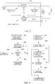
- Said power supply device with IIC bus in the abovementioned data card specifically comprises: DC power conversion unit 151, power input detection unit 152, state monitoring and logic control unit 153 and power output detection unit 154, as shown in FIG. 2 , wherein:
- said power supply device supplies power to the PA in said RF working unit
- said CPU detects the envelope of the output signal of PA in real time by the monitoring and managing bus, and converts the envelope signal into a control signal by using the CPU software algorithms, and transmits said control signal to said power supply device with IIC bus interface over the IIC bus, so that the amplitude of the output voltage of the power supply device with IIC bus interface follows the change in the envelope curve of the output signal of PA, which can improve the working efficiency of PA and reduce power consumption and heat dissipation of the PA in the data card.
- the abovementioned power supply device with IIC bus interface supplies power to the data card, and a combination of hardware and software can be used to realize the real-time dynamic interaction between the power supply and the load as well as between the power supply and the product end-users, thereby solving the problems of power consumption and heat dissipation of the products.
- the IIC bus interface can be used to achieve the communication between the CPU and the power supply device, therefore, detecting and controlling I/O ports can be multiplexed, that is, only two I/O ports are required, and the number of I/O ports does not increase with the increase of the detection or control amount, which overcomes the defects well in the related art that the mode of managing the power supply mostly adopts hardware configuration and it is not flexible enough.
- the embodiment of the present invention also provides a power supply device, and the structure of said power supply device is the same as that of the power supply device in the abovementioned data card, and as shown in FIG. 2 , it is not mentioned here; it should be noted that the PA in the RF working unit in FIG. 1 is one example of the load in FIG. 2 , and the person skilled in the art knows that said load can be replaced with another equipment or apparatus.
- the embodiment of the present invention further provides a method for power supply device managing the power supply, and said method comprises:
- FIG. 3 it is a flow chart of the power supply device with IIC interface managing the power supply in accordance with the present invention, and without special instructions, the left side of the figure can be understood as a flow chart of the CPU controlling and managing said power supply device with IIC interface, and it is mainly implemented by the CPU software (corresponding to the abovementioned step one), and the right side of the figure can be understood as the operating process of the power supply device with IIC interface, and the process of interacting with external information (including the user's manual settings, load parameters and so on), and it is achieved by using the hardware circuit of the power supply device with IIC interface (corresponding to the abovementioned step two).
- the operating process of the power supply device with IIC interface is as follows:
- the power supply works at the initial default state and outputs the default voltage and current parameters; the parameter register within said power supply device enters into the reset state and clears the values in the register; the embedded IIC bus interface and the initialized IIC bus are ready to communicate with the primary CPU implementing the power management.
- the CPU In the data card including the abovementioned power supply device, it needs the CPU to implement the function of power management by means of software. Wherein, communication is established between the CPU and the power supply device through the IIC bus. Said CPU achieves power management for said power supply device with IIC bus interface by means of software, and its process is as follows:
- two 6bit registers R [7:2] are used to store the adjustment difference and detection parameters of the amplitude of the output voltage.
- the minimum output voltage of the power supply is 3.5V, and the maximum output voltage 4.44V. That is, the maximum value 4.44V corresponds to the HEX number "62"; and 3.5V corresponds to the HEX number "00".
- Each minimum logic state of the registers corresponds to the minimum value, 0.02V, of the output voltage of said power supply, that is, the minimum resolution of the output voltage adjustment is 0.02V.
- a corresponding data table (hereinafter referred to as the output voltage mapping table) is provided in the CPU to perform mapping for a group of register values and output voltage values, and the corresponding relationship is as described above, and the CPU acquires the register setting values corresponding to the output voltage of the power supply by looking up the table, or it acquires the actual output voltage value of the power supply by reading the parameter register value in the power converter and looking up the table.
- the 5V power inputted through the USB bus interface (hereinafter referred to as VBUS) is sent to the power supply device with IIC bus 401, and the output voltage (3.5V-4.4V) converted by the power supply device is output to one end of the energy-storage inductor (L0) through the output end (the SW) of said DC power conversion unit, and the other end of L0 is connected with one end of the R SNS , and the other end of R SNS is connected with the drain of the switch tube Q, and the source of the switch tube Q is connected with the power supply end of the load PA (hereinafter referred to as VCC), and meanwhile, it can also be connected to a battery with the charging function for charging.
- VCC power supply end of the load PA
- the gate of the switch tube Q is connected to the GPIO of the CPU 402 in the system.
- Said CPU can implement the power supply on/off function on the PA and the rechargeable battery via the GPIO.
- Said R SNS is the power supply output current parameter detection apparatus, converting the output current into a voltage and sending the voltage to said power converter for output parameter detection;
- the IIC interface serial clock (SCL) and serial data (SDA) of the power converter are connected to the general GPIO pin or the IIC bus interface of the CPU in the system;
- the charging state indication signal (STAT) of the power converter is connected to another GPIO port of the CPU in the system, which is used to monitor the state of the power converter charging the battery load, and said power converter is in the charging state, and the signal outputs logic high level, and after the charging finishes, the signal outputs logic low level.
- the input end of the envelope detection device 403 is connected to the output end of the RF power amplifier (hereinafter referred to as PA) 404, and the output end of said envelope detection device is connected to the input end of the high-speed analog-to-digital converter (ADC) of the CPU in the system.
- PA RF power amplifier
- ADC analog-to-digital converter
- the current absorbed by the PA from the power supply during operation remains substantially constant, even if the VCC voltage changes; if the PA outputs a higher level signal, the PA must also provide a higher VCC voltage in order to maintain the linearity; if the supply voltage VCC of PA remains unchanged, the PA is required to have sufficient linearity, so that the maximum power level output by the PA can meet the requirements of system, and the distortion will not be produced in the signal power amplification and so on. Therefore, it raises relatively high requirements for the PA itself.
- the power supply is bound to provide relatively high voltage VCC, as shown in FIG.
- the efficiency curve of PA in this design represents that, when the output power level of PA is higher, the efficiency of PA is higher, while when the output power level of PA is lower, the lower the efficiency of PA is (it requires said VCC to have the higher voltage). This is extremely unfavorable to the power consumption and heat dissipation of the products.
- the VCC of the PA is connected to the power supply device with IIC bus interface, and the power supply of the PA establishes a communication with the primary CPU, and it is controlled by the CPU in real time, and the envelope detection device samples the output signal of the PA in the RF working unit, and performs the amplitude detection on the sampled signal.
- the detection of the envelope detection device outputs the envelope signal to the ADC interface of the CPU, and the ADC interface performs the high-speed sampling and A/D conversion on the detection signal, that is, the digital processing is performed on the envelope signal, and the A/D digitized bite data is stored in the memory of the CPU, and said CPU compares the digitized bite data converted from the envelope signal with the data in the abovementioned output voltage mapping table in real time, that is, it needs to search out the data equal to or slightly greater than its own data. Then, the CPU writes said data in the voltage mapping table into the power supply device by the IIC bus, such that the output voltage of said power supply device is adjusted with the amplitude of the output signal of PA, the waveform of the power supply VCC shown in FIG.
- the output voltage of the power supply device can be automatically adjusted in real time with the amplitude of the output signal of PA. This can improve the efficiency of conversion between the power supply of PA shown in FIG. 4 , that is, the power supply device with IIC bus, and the PA output in the RF working unit, thereby reducing the PA's own power consumption and heat dissipation, and also extending the service life of the power supply device.
- the power supply device with IIC bus can flexibly communicate with the CPU having powerful software and hardware resources, to achieve the real-time detection and control of the power supply, and to achieve a variety of power management requirements, and it can reduce the power consumption of the data card and solve the heat dissipation problem of wireless communication terminals such as data cards in a relatively good way.
- the abovementioned power supply device, the method for managing power supply thereof and the wireless communication terminal can flexibly communicate with a CPU having strong software and hardware resources, to achieve the real-time detection and control of the power supply, to achieve a variety of power management requirements, to reduce power consumption of the wireless communication terminals, and to solve the heat dissipation problem of the wireless communication terminals in a relatively good way.
Landscapes
- Engineering & Computer Science (AREA)
- Power Engineering (AREA)
- Computer Networks & Wireless Communication (AREA)
- Signal Processing (AREA)
- Power Sources (AREA)
- Direct Current Feeding And Distribution (AREA)
- Control Of Voltage And Current In General (AREA)
- Transmitters (AREA)
Description
- The present invention relates to the field of power supply management, and more particularly, to a power supply device, a method for managing power supply thereof, and a wireless communication terminal.
- Power conversion module is the core part of data card products and plays a decisive role in the price-performance ratio of the data card products. Continuous power technology innovation and individual needs of the power technology have long been the objectives focused and pursued by product research and development engineers. The traditional data card, the method for supplying power to the data cards, and the method for managing the power supply are shown in
FIG. 1a , and its main characteristics are embodied in the following aspects:
the data card mainly comprises a baseband working unit and a radio frequency (RF) working unit, the power supply of the abovementioned two workings units is provided by an external input power supply of the data card outputting an appropriate power to supply power for the baseband and RF working units through a single-chip DC power converter. - The abovementioned data card and its method for supplying power have advantages of simple structure and low cost, but meanwhile they have the following problems:
- 1, the output power of power supply of the conventional data card cannot dynamically adapt to the change of load and cannot automatically adjust the output power of the power supply device in real time, especially when supplying power to the power amplifier (hereinafter referred to as PA) in the RF circuits, the power supply device of the traditional data card and the management method thereof cannot perform the adjustment dynamically with the change of the output load of the amplifier, thus it is difficult to solve the power consumption and heat dissipation problems of the products.
- 2, in the traditional data products, the communication between the power supply device and the main central processing unit (CPU) mainly adopts the CPU's general-purpose input/output (GPIO) ports for implementation. That is, the CPU needs to use some of the input/output (I/O) ports for the parameter detection of the power supply module, and use the other I/O ports for the control of the power supply module. Obviously, when the detected parameters or control amount increases, the number of I/O ports used by the CPU increases dramatically. The method also increases the complexity of system, taking up a lot of CPU hardware resources, and meanwhile it also increases the physical space of the circuit board, not suitable for compact design of the terminal products.
- 3, the conventional data card products often lack the real-time monitoring and centralized management of the CPU for core components such as the power conversion device and the charging management device in the system to enhance the reliability and flexibility of system.
- Product research and development engineers want to use a device to monitor and manage the power supply module in real time via the CPU in the system, to solve the abovementioned problems and enhance the flexibility and reliability of system. However, the existing technical solutions cannot meet the abovementioned requirements very well.
- Document
WO 2004070941 A2 discloses embodiments of RF power amplifiers that include switched-mode power amplifiers supplied by synchronous buck DC-DC converters. The switched-mode power amplifiers can be used to amplify a limited form of an RF input signal and the supply to the switched-mode power amplifier is varied in response to the envelope of the RF input signal. However, the abovementioned problems still remain unsolved in this document. - The present invention is defined by the features of claim 1. More specifically, the embodiment of the present invention provides a power supply device, a method for managing power supply thereof, and a wireless communication terminal to solve power consumption and heat dissipation problems of power amplifier (PA) in a wireless communication terminal such as current data card.
- The embodiment of the present invention provides a wireless communication terminal, comprising a baseband working unit and a radio frequency (RF) working unit, and a direct current (DC) power converter connected with both said baseband working unit and said RF working unit, and said wireless communication terminal further comprises: a power supply device, a central processing unit (CPU), an Inter Integrated Circuit bus connecting the power supply device to the CPU, and an envelope detection device, wherein:
- said power supply device comprises an Inter Integrated Circuit bus interface and is configured to receive a voltage supplied by said DC power converter, provide an output voltage to a power amplifier (PA) in said RF working unit, receive a control signal sent by said CPU through the Inter Integrated Circuit bus, and adjust said output voltage according to said control signal, so that an amplitude of the output voltage of said power supply device with the Inter Integrated Circuit bus interface follows change in an envelope curve of an output signal of said PA;
- said envelope detection device is connected with said RF working unit, and it is configured to detect an envelope signal of said output signal of PA in real time, and send said envelope signal to said CPU;
- said CPU is connected respectively with said DC power converter, said power supply device and said envelope detection device, and it is configured to: receive a voltage provided by said DC power converter, convert said envelope signal sent by said envelope detection device into a control signal, and send said converted control signal to said power supply device.
- Preferably, said CPU is further configured to convert the information inputted via a human-machine interface of said wireless communication terminal into a control signal, and send said converted control signal to said power supply device.
- Preferably, said CPU is connected with said power supply device by IIC bus.
- Preferably, said power supply device comprises a DC power conversion unit, a power input detection unit, a state monitoring and logic control unit and a power output detection unit, wherein:
- said DC power supply conversion unit is configured to receive said voltage input by said DC power converter, provide an output voltage to said PA, receive a logic control signal sent by said state monitoring and logic control unit, and adjust said output voltage in accordance with said logic control signal;
- said power input detection unit is configured to detect an input signal of said DC power conversion unit, and send an input detection result to said state monitoring and logic control unit;
- said power output detection unit is configured to detect an output signal of said DC power conversion unit, and send an output detection result to said state monitoring and logic control unit;
- said state monitoring and logic control unit is configured to receive said control signal sent by said CPU, compare any one of said input detection result sent by said power input detection unit and the output detection result sent by said power output detection unit with said control signal, if the two are inconsistent, send a logic control signal to said DC power conversion unit.
- Preferably, said state monitoring and logic control unit is implemented with a state machine.
- The abovementioned power supply device, the method for managing power supply thereof and the wireless communication terminal can flexibly communicate with a CPU having strong software and hardware resources, to achieve the real-time power detection and control, to achieve a variety of power management needs, to reduce power consumption of the wireless communication terminals, and to solve the heat dissipation problem of the wireless communication terminals.
-
-
FIG. 1a is a diagram of the architecture of a traditional data card and its mode of power supply; -
FIG. 1b is an architectural diagram of a data card powered by a power supply device with IIC interface in accordance with the present invention; -
FIG. 2 is an architectural schematic diagram of a power supply device with IIC interface in accordance with the present invention; -
FIG. 3 is a flow chart of the power supply device with IIC interface managing the power supply in accordance with the present invention; -
FIG. 4 is a specific embodiment of data card power management of the power supply device with IIC interface in accordance with the present invention; -
FIG. 5 is a schematic diagram of the working power supply VCC of the PA in a traditional RF working unit; -
FIG. 6 is a schematic diagram of the PA's power supply VCC managed by the data card power supply of the power supply unit with IIC interface in accordance with the present invention; -
FIG. 7 is a diagram of comparing the traditional mode of power supply with the current curve of the data card PA power supply in the device in accordance with the present invention. - To make the objectives, technical solutions and advantages of the present invention more clear, hereinafter the embodiments of the present invention would be described in detail with combination of the accompanying drawings. It should be noted that, in the case of no conflict, the embodiments in the present application and features in the embodiments can be combined arbitrarily with each other.
- The embodiment of the present invention provides a wireless communication terminal comprising a baseband working unit, a RF working unit and a DC power converter connected with said baseband working unit and said RF working unit, and said wireless communication terminal further comprises: a power supply device, a central processing unit (CPU) and an envelope detection device, wherein:
- said power supply device is located between said DC power converter and said RF working unit, and it is configured to receive a voltage provided by said DC power converter, provide an output voltage to the power amplifier (PA) in said RF working unit, receive a control signal sent by said CPU, and adjust said output voltage according to said control signal, so that said output voltage meets the envelope variation curve of output signal of said PA;
- said envelope detection device is connected with said RF working unit, and it is configured to monitor the envelope signal of said output signal of said PA in real time, and send said envelope signal to said CPU;
- said CPU is connected respectively with said DC power converter, said power supply device and said envelope detection device, and it is configured to receive the voltage provided by said DC power converter, convert said envelope signal sent by said envelope detection device into a control signal, and send said control signal to said power supply device.
- Wherein, said CPU is further configured to convert the information inputted via the human-machine interface of said card data into said control signal, and send said control signal to said power supply device.
- Preferably, said CPU is connected with said power supply device by the IIC (Inter Integrated Circuit) bus.
- The abovementioned wireless communication terminal can be a data card or other product, and in the following, the data card is taken as an example to describe in detail the technical solutions in accordance with the embodiment of the present invention:
As shown inFIG. 1b , it is an architectural diagram of the data card powered by a power supply device with IIC interface in accordance with the present invention, and said data card comprises:baseband working unit 11,RF working unit 12,DC power converter 13, CPU14, andpower supply device 15 with IIC bus. Wherein, the thin black line indicates the data transmission path of the communications products, the thick black line indicates the power supply path, and the thin dashed line indicates the bus over which said CPU monitors and manages various function modules. The data input end of said baseband working unit is connected to the USB socket through the USB cable, and the output end of said baseband working unit is connected with the input end of said RF working unit, and the output end of said RF working unit is connected with communication transmitting antenna through the antenna interface. The 5V input power of said data card is first sent to said DC power converter, and the converted DC power is sent respectively to said baseband working unit, said CPU, and said power supply device with IIC bus. Wherein, the power supply device with IIC bus supplies power to the power amplifier (hereinafter referred to as PA) in said RF working unit. The primary CPU establishes a communication with said power supply device over the IIC bus, connects with said RF working unit and said baseband working unit by a monitoring and managing bus, and monitors and manages the operating state of said RF working unit and said baseband working unit. - Said power supply device with IIC bus in the abovementioned data card specifically comprises: DC
power conversion unit 151, powerinput detection unit 152, state monitoring andlogic control unit 153 and poweroutput detection unit 154, as shown inFIG. 2 , wherein: - the input end of the abovementioned DC power conversion unit is connected with the power supply, and its output end is connected with the power supply load, implementing converting the input power into an output power that meets the needs of load; the unit further comprises a controlled input interface, and it is configured to receive the logic control signal sent by said state monitoring and logic control unit; specifically, it is configured to receive the voltage input by said DC power converter, provide the output voltage to said PA, receive the logic control signal sent by the state monitoring and logic control unit, and adjust the output voltage of said DC power conversion unit according to said logic control signal;
- the input end of the abovementioned power input detection unit is connected with the input end of said DC power conversion unit, and its output end is connected with said state monitoring and logic control unit, and it is configured to perform detection on the input signal of said DC power conversion unit, and send the input detection result to said state monitoring and logic control unit;
- the input end of the abovementioned power output detection device is connected with the output end of said DC power conversion unit, and its output end is connected with said state monitoring and logic control unit, and it is configured to perform detection on the output signal of said DC power conversion unit and send the output detection result to said state monitoring and logic control unit;
- the input end of the abovementioned state monitoring and logic control unit is respectively connected with said power input detection unit and said power output detection unit, and its output end is connected with said DC power conversion unit, and it is configured to store the detection results of said power input detection unit and said power output detection unit; compare any one of said input detection result sent by said power input detection unit and the output detection result sent by said power output detection unit with said control signal, if the two are inconsistent, send a logic control signal to said DC power conversion unit, to achieve functions such as the state control of said DC power conversion unit.
- The process of said data card managing the power supply is as follows:
said power supply device supplies power to the PA in said RF working unit, and said CPU detects the envelope of the output signal of PA in real time by the monitoring and managing bus, and converts the envelope signal into a control signal by using the CPU software algorithms, and transmits said control signal to said power supply device with IIC bus interface over the IIC bus, so that the amplitude of the output voltage of the power supply device with IIC bus interface follows the change in the envelope curve of the output signal of PA, which can improve the working efficiency of PA and reduce power consumption and heat dissipation of the PA in the data card. - The abovementioned power supply device with IIC bus interface supplies power to the data card, and a combination of hardware and software can be used to realize the real-time dynamic interaction between the power supply and the load as well as between the power supply and the product end-users, thereby solving the problems of power consumption and heat dissipation of the products. In addition, the IIC bus interface can be used to achieve the communication between the CPU and the power supply device, therefore, detecting and controlling I/O ports can be multiplexed, that is, only two I/O ports are required, and the number of I/O ports does not increase with the increase of the detection or control amount, which overcomes the defects well in the related art that the mode of managing the power supply mostly adopts hardware configuration and it is not flexible enough.
- Furthermore, the embodiment of the present invention also provides a power supply device, and the structure of said power supply device is the same as that of the power supply device in the abovementioned data card, and as shown in
FIG. 2 , it is not mentioned here; it should be noted that the PA in the RF working unit inFIG. 1 is one example of the load inFIG. 2 , and the person skilled in the art knows that said load can be replaced with another equipment or apparatus. - The embodiment of the present invention further provides a method for power supply device managing the power supply, and said method comprises:
- step one, said power management device achieves the expected operating parameters;
- step two, said power management unit acquires the output voltage provided to the load in real time, comparing said output voltage with said expected operating parameters, and if the two are consistent, said output voltage is continued to be provided to said load, if the two are inconsistent, said output voltage is adjusted according to the expected operating parameters, so that said output voltage meets the needs of load.
- As shown in
FIG. 3 , it is a flow chart of the power supply device with IIC interface managing the power supply in accordance with the present invention, and without special instructions, the left side of the figure can be understood as a flow chart of the CPU controlling and managing said power supply device with IIC interface, and it is mainly implemented by the CPU software (corresponding to the abovementioned step one), and the right side of the figure can be understood as the operating process of the power supply device with IIC interface, and the process of interacting with external information (including the user's manual settings, load parameters and so on), and it is achieved by using the hardware circuit of the power supply device with IIC interface (corresponding to the abovementioned step two). - The operating process of the power supply device with IIC interface is as follows:
-
step 301a, the power supply device is initially powered on; -
step 302a, with the hardware circuit settings, the default transient output of the power supply is configured as 3.6V-4.2V; - After said power supply device is powered on, the power supply works at the initial default state and outputs the default voltage and current parameters; the parameter register within said power supply device enters into the reset state and clears the values in the register; the embedded IIC bus interface and the initialized IIC bus are ready to communicate with the primary CPU implementing the power management.
-
step 303a, the power input/output parameter detection unit sends the real-time collected parameters to the state and parameter registers, providing them to the primary CPU for inquiry in real-time, and the primary CPU implementing power management reads the parameters in the state and parameter registers via the IIC bus and acquires the operating state of the power supply; -
step 304a, the state monitoring and logic control unit (implemented with a state machine) in the power supply unit with IIC interface accepts the control parameters transferred by said CPU over the IIC bus, and by comparing the control parameters transferred by the CPU with the state parameters of the DC/DC DC conversion unit detected by the power supply device itself and judging whether the two are consistent or not, it is determined whether it needs to adjust accordingly the output parameters of said DC/DC DC conversion unit or not, so as to adapt to the dynamic change of the load and the user parameter settings, if no, proceeding to step 302a and the DC power is output and supplied to the load according to the default method, otherwise, proceeding to step 305a, meanwhile, continuing to acquire the state parameters of said DC conversion unit; -
step 305a, in accordance with the requirements of the CPU control parameters or the parameters manually set by the user, the DC power is output and supplied to said load. - In the data card including the abovementioned power supply device, it needs the CPU to implement the function of power management by means of software. Wherein, communication is established between the CPU and the power supply device through the IIC bus. Said CPU achieves power management for said power supply device with IIC bus interface by means of software, and its process is as follows:
-
step 301b, said CPU starts said power management module; -
step 302b, said CPU power management module initializes said IIC bus, establishing a communication with said power supply device with IIC bus interface, and it reads the parameter of the operating state of the power supply through the IIC bus; -
step 303b, said CPU can accept the information of the power supply user's needs, for example, said power supply is in the state of charging the battery, the user can set parameters such as charging current and charging time via the human-machine interface in said data card in accordance with the present invention; or it accepts the changing dynamic information of the load powered by power supply, and the information primarily comprises the power consumption curve of the load, the required current or voltage curve and so on; -
step 304b, said CPU performs the comprehensive judgment according to the information of the operating state of power supply, the power supply user's needs and the change of the load powered by the power supply and so on, and it is determined whether it needs to adjust the power supply output parameters or not, if it does not need to perform the adjustment, returning to step 302b, otherwise, proceeding to step 305b; -
step 305b, the CPU outputs the power supply control parameters, and sends them to the power supply device with IIC bus interface over the IIC bus, to make the output power meet the requirements. - Wherein, two 6bit registers R [7:2] are used to store the adjustment difference and detection parameters of the amplitude of the output voltage. The minimum output voltage of the power supply is 3.5V, and the maximum output voltage 4.44V. That is, the maximum value 4.44V corresponds to the HEX number "62"; and 3.5V corresponds to the HEX number "00". Each minimum logic state of the registers corresponds to the minimum value, 0.02V, of the output voltage of said power supply, that is, the minimum resolution of the output voltage adjustment is 0.02V. Therefore, a corresponding data table (hereinafter referred to as the output voltage mapping table) is provided in the CPU to perform mapping for a group of register values and output voltage values, and the corresponding relationship is as described above, and the CPU acquires the register setting values corresponding to the output voltage of the power supply by looking up the table, or it acquires the actual output voltage value of the power supply by reading the parameter register value in the power converter and looking up the table.
- To further illustrate the structure of the power supply device and the data card including the power supply device in accordance with the present invention, a specific embodiment will be described in the following for illustration, as shown in
FIG. 4 :
in this embodiment, the 5V power inputted through the USB bus interface (hereinafter referred to as VBUS) is sent to the power supply device withIIC bus 401, and the output voltage (3.5V-4.4V) converted by the power supply device is output to one end of the energy-storage inductor (L0) through the output end (the SW) of said DC power conversion unit, and the other end of L0 is connected with one end of the RSNS, and the other end of RSNS is connected with the drain of the switch tube Q, and the source of the switch tube Q is connected with the power supply end of the load PA (hereinafter referred to as VCC), and meanwhile, it can also be connected to a battery with the charging function for charging. The gate of the switch tube Q is connected to the GPIO of theCPU 402 in the system. Said CPU can implement the power supply on/off function on the PA and the rechargeable battery via the GPIO. Said RSNS is the power supply output current parameter detection apparatus, converting the output current into a voltage and sending the voltage to said power converter for output parameter detection; the IIC interface serial clock (SCL) and serial data (SDA) of the power converter are connected to the general GPIO pin or the IIC bus interface of the CPU in the system; the charging state indication signal (STAT) of the power converter is connected to another GPIO port of the CPU in the system, which is used to monitor the state of the power converter charging the battery load, and said power converter is in the charging state, and the signal outputs logic high level, and after the charging finishes, the signal outputs logic low level. The input end of theenvelope detection device 403 is connected to the output end of the RF power amplifier (hereinafter referred to as PA) 404, and the output end of said envelope detection device is connected to the input end of the high-speed analog-to-digital converter (ADC) of the CPU in the system. - According to the traditional power management design project, there are: the current absorbed by the PA from the power supply during operation remains substantially constant, even if the VCC voltage changes; if the PA outputs a higher level signal, the PA must also provide a higher VCC voltage in order to maintain the linearity; if the supply voltage VCC of PA remains unchanged, the PA is required to have sufficient linearity, so that the maximum power level output by the PA can meet the requirements of system, and the distortion will not be produced in the signal power amplification and so on. Therefore, it raises relatively high requirements for the PA itself. However, in order to maintain the linearity of PA on the premise that the breakthrough improvement does not exist in the performance of the existing PA itself, the power supply is bound to provide relatively high voltage VCC, as shown in
FIG. 5 , while the currents required by the PA remains unchanged. The efficiency curve of PA in this design represents that, when the output power level of PA is higher, the efficiency of PA is higher, while when the output power level of PA is lower, the lower the efficiency of PA is (it requires said VCC to have the higher voltage). This is extremely unfavorable to the power consumption and heat dissipation of the products. - As shown in
FIG. 4 , the VCC of the PA is connected to the power supply device with IIC bus interface, and the power supply of the PA establishes a communication with the primary CPU, and it is controlled by the CPU in real time, and the envelope detection device samples the output signal of the PA in the RF working unit, and performs the amplitude detection on the sampled signal. The detection of the envelope detection device outputs the envelope signal to the ADC interface of the CPU, and the ADC interface performs the high-speed sampling and A/D conversion on the detection signal, that is, the digital processing is performed on the envelope signal, and the A/D digitized bite data is stored in the memory of the CPU, and said CPU compares the digitized bite data converted from the envelope signal with the data in the abovementioned output voltage mapping table in real time, that is, it needs to search out the data equal to or slightly greater than its own data. Then, the CPU writes said data in the voltage mapping table into the power supply device by the IIC bus, such that the output voltage of said power supply device is adjusted with the amplitude of the output signal of PA, the waveform of the power supply VCC shown inFIG. 4 is shown inFIG. 6 . Therefore, the output voltage of the power supply device can be automatically adjusted in real time with the amplitude of the output signal of PA. This can improve the efficiency of conversion between the power supply of PA shown inFIG. 4 , that is, the power supply device with IIC bus, and the PA output in the RF working unit, thereby reducing the PA's own power consumption and heat dissipation, and also extending the service life of the power supply device. - In short, the power supply device with IIC bus can flexibly communicate with the CPU having powerful software and hardware resources, to achieve the real-time detection and control of the power supply, and to achieve a variety of power management requirements, and it can reduce the power consumption of the data card and solve the heat dissipation problem of wireless communication terminals such as data cards in a relatively good way.
- Those ordinarily skilled in the art can understand that all or some of steps in the above-mentioned method may be completed by programs instructing the relevant hardware, and said programs may be stored in a computer-readable storage medium, such as read only memory, magnetic or optical disk. Optionally, all or some of the steps in the above-mentioned embodiments may also be implemented by using one or more integrated circuits. Accordingly, each module/unit in the above-mentioned embodiment may be realized in the form of hardware or software function modules. The present invention is not limited to any specific form of hardware and software combinations.
- The abovementioned power supply device, the method for managing power supply thereof and the wireless communication terminal can flexibly communicate with a CPU having strong software and hardware resources, to achieve the real-time detection and control of the power supply, to achieve a variety of power management requirements, to reduce power consumption of the wireless communication terminals, and to solve the heat dissipation problem of the wireless communication terminals in a relatively good way.
Claims (5)
- A wireless communication terminal, comprising a baseband working unit (11) and a radio frequency, RF, working unit (12), and a direct current, DC, power converter (13) connected with both said baseband working unit (11) and said RF working unit (12), said wireless communication terminal further comprising: a central processing unit, CPU, (14;402) and an envelope detection device (403), wherein:said envelope detection device (403) is connected with said RF working unit (12) and is configured to detect an envelope signal of the output signal of a power amplifier, PA, (404) comprised in said RF working unit in real time, and send said envelope signal to said CPU (14;402);said CPU (14;402) is connected respectively with said DC power converter (13) and said envelope detection device (403), and the CPU (14;402) is configured to: receive a voltage provided by said DC power converter (13), and convert said envelope signal sent by said envelope detection device (403) into a control signal;characterized in that the wireless communication terminal further comprises a power supply device (15;401) and an Inter Integrated Circuit bus connecting the power supply device (15;401) to the CPU (14;402);in that said power supply device (15;401) comprises an Inter Integrated Circuit bus interface and is configured to provide an output voltage to the power amplifier, PA, (404) in said RF working unit (12), receive a control signal sent by said CPU (14) through the Inter Integrated Circuit bus, and adjust said output voltage according to said control signal, so that an amplitude of the output voltage of said power supply device (15;401) with the Inter Integrated Circuit bus interface follows change in an envelope curve of an output signal of said PA (404);and in that said CPU (14;402) is configured to send the converted control signal to said power supply device (15;401).
- The wireless communication terminal of claim 1, wherein:
said CPU (14;402) is further configured to convert information inputted via a human-machine interface of said wireless communication terminal into a control signal, and send the converted control signal to said power supply device (15;401). - The wireless communication terminal of claim 1 or 2, wherein:
said CPU (14;402) is connected with said power supply device (15;401) by Inter Integrated Circuit, IIC, bus. - The wireless communication terminal of claim 3, wherein:said power supply device (15) comprises a DC power conversion unit (151), a power input detection unit (152), a state monitoring and logic control unit (153) and a power output detection unit (154), wherein:said DC power conversion unit (151) is configured to receive a voltage input by said DC power converter (13), provide an output voltage to said PA (404), receive a logic control signal sent by said state monitoring and logic control unit (153), and adjust said output voltage in accordance with said logic control signal;said power input detection unit (152) is configured to perform detection on an input signal of said DC power conversion unit (151), and send an input detection result to said state monitoring and logic control unit (153);said power output detection unit (154) is configured to perform detection on an output signal of said DC power conversion unit (151), and send an output detection result to said state monitoring and logic control unit (153);said state monitoring and logic control unit (153) is configured to receive the control signal sent by said CPU (14;402), compare any one of said input detection result sent by said power input detection unit (152) and the output detection result sent by said power output detection unit (154) with said control signal, if the two are inconsistent, send the logic control signal to said DC power conversion unit (151).
- The wireless communication terminal of claim 4, wherein:
said state monitoring and logic control unit (153) is implemented with a state machine.
Applications Claiming Priority (2)
| Application Number | Priority Date | Filing Date | Title |
|---|---|---|---|
| CN201210009131.7A CN102571131B (en) | 2012-01-12 | 2012-01-12 | Power supply device, method for managing power supply thereof and wireless communication terminal |
| PCT/CN2012/073510 WO2013104149A1 (en) | 2012-01-12 | 2012-04-05 | Power supply device, method for managing power supply thereof and wireless communication terminal |
Publications (3)
| Publication Number | Publication Date |
|---|---|
| EP2804442A1 EP2804442A1 (en) | 2014-11-19 |
| EP2804442A4 EP2804442A4 (en) | 2015-09-30 |
| EP2804442B1 true EP2804442B1 (en) | 2018-08-15 |
Family
ID=46415705
Family Applications (1)
| Application Number | Title | Priority Date | Filing Date |
|---|---|---|---|
| EP12864832.6A Active EP2804442B1 (en) | 2012-01-12 | 2012-04-05 | Power supply device, method for managing power supply thereof and wireless communication terminal |
Country Status (6)
| Country | Link |
|---|---|
| US (1) | US9166478B2 (en) |
| EP (1) | EP2804442B1 (en) |
| JP (1) | JP2015510310A (en) |
| KR (1) | KR20140111342A (en) |
| CN (1) | CN102571131B (en) |
| WO (1) | WO2013104149A1 (en) |
Families Citing this family (10)
| Publication number | Priority date | Publication date | Assignee | Title |
|---|---|---|---|---|
| CN103872751B (en) * | 2012-12-18 | 2016-12-28 | 中磊电子(苏州)有限公司 | Electric supply installation and wireless network communications system |
| TW201526491A (en) * | 2013-12-31 | 2015-07-01 | Ibm | Efficiency adjustments in power supply system |
| CN104391556A (en) * | 2014-11-13 | 2015-03-04 | 英业达科技有限公司 | Power supply protection device and method |
| CN107196614A (en) * | 2017-05-22 | 2017-09-22 | 湖北凯乐科技股份有限公司 | Have Larger Dynamic output power range and efficient RF power amplification device concurrently |
| CN111684699B (en) * | 2017-10-31 | 2024-05-10 | 骆武宁 | Communication control power supply |
| CN111800305B (en) * | 2019-04-09 | 2023-12-15 | 中兴通讯股份有限公司 | A heat dissipation test method, system and heating device |
| CN111817538B (en) * | 2020-07-15 | 2021-10-01 | 中国核动力研究设计院 | Multi-channel power adapter of two-wire system connection charge converter and application method |
| CN113624345A (en) * | 2021-08-16 | 2021-11-09 | 合肥芯福传感器技术有限公司 | Infrared thermal imaging device and imaging method based on event detection |
| CN113596359A (en) * | 2021-08-16 | 2021-11-02 | 合肥芯福传感器技术有限公司 | Single photon imaging equipment and imaging method based on event detection |
| CN115102568B (en) * | 2022-07-12 | 2023-10-24 | 东集技术股份有限公司 | Radio frequency circuit, control method and device, radio frequency read-write equipment and storage medium |
Family Cites Families (42)
| Publication number | Priority date | Publication date | Assignee | Title |
|---|---|---|---|---|
| JP2689011B2 (en) * | 1990-02-13 | 1997-12-10 | 日本電信電話株式会社 | Linear transmitter |
| JPH05267941A (en) * | 1992-03-18 | 1993-10-15 | Sanyo Electric Co Ltd | High efficiency type high frequency power amplifier |
| JP3136382B2 (en) * | 1992-10-19 | 2001-02-19 | 京セラ株式会社 | Linear transmitter |
| JP2842267B2 (en) * | 1994-12-30 | 1998-12-24 | 日本電気株式会社 | Portable radio |
| JP3249418B2 (en) * | 1997-02-27 | 2002-01-21 | 三洋電機株式会社 | Power supply, wireless device |
| JP3438126B2 (en) * | 1997-10-31 | 2003-08-18 | 富士通アクセス株式会社 | DC / DC converter |
| US6141541A (en) * | 1997-12-31 | 2000-10-31 | Motorola, Inc. | Method, device, phone and base station for providing envelope-following for variable envelope radio frequency signals |
| US6407634B1 (en) * | 2000-06-16 | 2002-06-18 | Motorola, Inc. | Linear envelope tracking RF power amplifier with adaptive analog signal processing |
| US6683496B2 (en) | 2001-08-20 | 2004-01-27 | Harris Corporation | System and method for minimizing dissipation in RF power amplifiers |
| JP2003124839A (en) * | 2001-09-28 | 2003-04-25 | Internatl Business Mach Corp <Ibm> | Transmitting and receiving method, transmission and reception card, and portable information terminal |
| JP2003133972A (en) * | 2001-10-29 | 2003-05-09 | Fujitsu Ltd | Electronic device having a wireless transmitter |
| JP3838547B2 (en) | 2001-12-11 | 2006-10-25 | 株式会社ルネサステクノロジ | Power supply device for high frequency power amplifier circuit |
| KR100553252B1 (en) * | 2002-02-01 | 2006-02-20 | 아바고테크놀로지스코리아 주식회사 | Power amplifier of portable terminal |
| JP2003235252A (en) * | 2002-02-08 | 2003-08-22 | Toyota Motor Corp | Power supply circuit |
| JP3865224B2 (en) * | 2002-03-15 | 2007-01-10 | 株式会社デンソー | Electric power steering device |
| US6914487B1 (en) * | 2002-04-19 | 2005-07-05 | National Semiconductor Corporation | Method and system for providing power management in a radio frequency power amplifier using adaptive envelope tracking |
| JP2003330549A (en) * | 2002-05-10 | 2003-11-21 | Hitachi Ltd | Semiconductor integrated circuit, power supply circuit and information recording medium |
| US7372333B2 (en) * | 2003-02-03 | 2008-05-13 | Arizona Board Of Regents, Acting For And On Behalf Of Arizona State University | Monolithic supply-modulated RF power amplifier and DC-DC power converter IC |
| GB2398648B (en) * | 2003-02-19 | 2005-11-09 | Nujira Ltd | Power supply stage for an amplifier |
| US7276966B1 (en) | 2003-10-28 | 2007-10-02 | Stmicroelectronics N.V. | Radio frequency envelope apparatus and method |
| JP2005223552A (en) * | 2004-02-04 | 2005-08-18 | Sharp Corp | Radio communication circuit and radio communication apparatus using the same |
| JP4497470B2 (en) * | 2004-09-17 | 2010-07-07 | ソニー・エリクソン・モバイルコミュニケーションズ株式会社 | High frequency power amplifier and transmitter |
| US7446514B1 (en) * | 2004-10-22 | 2008-11-04 | Marvell International Ltd. | Linear regulator for use with electronic circuits |
| WO2007114951A2 (en) * | 2006-04-04 | 2007-10-11 | Cerus Industrial Corporation | Apparatus, system, and/or method for protection and control of an electrical device |
| US20080003962A1 (en) | 2006-06-30 | 2008-01-03 | Wai Lim Ngai | Method and apparatus for providing adaptive supply voltage control of a power amplifier |
| JP4899696B2 (en) * | 2006-07-31 | 2012-03-21 | 富士通株式会社 | Communication device, relay device, communication system, communication method, and communication program |
| JP2009088620A (en) * | 2007-09-27 | 2009-04-23 | Rohm Co Ltd | Radio communication terminal and control method thereof |
| WO2009059459A1 (en) * | 2007-11-07 | 2009-05-14 | Texas Instruments Incorporated | A power regulator system with current limit independent of duty cycle and its regulation method |
| US20090323985A1 (en) * | 2008-06-30 | 2009-12-31 | Qualcomm Incorporated | System and method of controlling power consumption in response to volume control |
| JP2010074407A (en) | 2008-09-17 | 2010-04-02 | Toshiba Corp | Bias controlling apparatus |
| US7872527B2 (en) * | 2009-03-31 | 2011-01-18 | Qualcomm, Incorporated | Power supply control system and method with variable post-regulation |
| JP5882574B2 (en) * | 2009-12-10 | 2016-03-09 | キヤノン株式会社 | High voltage power supply device and image forming apparatus having the same |
| CN102136846B (en) * | 2010-01-21 | 2013-11-06 | 天津里外科技有限公司 | Power management device and method |
| CN102148563B (en) * | 2010-02-10 | 2014-01-01 | 华为技术有限公司 | Tracking power supply, power control method and communication equipment |
| US8194869B2 (en) * | 2010-03-17 | 2012-06-05 | Harman International Industries, Incorporated | Audio power management system |
| US8174313B2 (en) | 2010-05-17 | 2012-05-08 | Avago Technologies Wireless Ip (Singapore) Pte. Ltd. | Apparatus and method for controlling power amplifier |
| US8406706B2 (en) * | 2010-05-20 | 2013-03-26 | Lg Electronics Inc. | Mobile terminal and method of controlling a driving voltage of a power amplifier therein |
| JP5735758B2 (en) * | 2010-05-25 | 2015-06-17 | キヤノン株式会社 | Voltage transformer type high voltage power supply device, high voltage power supply device, and image forming apparatus |
| US8183917B2 (en) * | 2010-06-04 | 2012-05-22 | Quantance, Inc. | RF power amplifier circuit with mismatch tolerance |
| CN102299567B (en) * | 2010-06-24 | 2013-11-06 | 海尔集团公司 | Electronic device and wireless power supply system and method thereof |
| CN102075149B (en) * | 2010-12-03 | 2013-01-23 | 哈尔滨工业大学深圳研究生院 | Power envelope tracing power supply of multi-phase interleaving radio-frequency power amplifier |
| CN102118516A (en) * | 2011-01-13 | 2011-07-06 | 中兴通讯股份有限公司 | Control method and system for output voltage of power management chip |
-
2012
- 2012-01-12 CN CN201210009131.7A patent/CN102571131B/en active Active
- 2012-04-05 WO PCT/CN2012/073510 patent/WO2013104149A1/en not_active Ceased
- 2012-04-05 JP JP2014551497A patent/JP2015510310A/en active Pending
- 2012-04-05 EP EP12864832.6A patent/EP2804442B1/en active Active
- 2012-04-05 US US14/371,830 patent/US9166478B2/en active Active
- 2012-04-05 KR KR1020147022259A patent/KR20140111342A/en not_active Ceased
Non-Patent Citations (1)
| Title |
|---|
| None * |
Also Published As
| Publication number | Publication date |
|---|---|
| CN102571131B (en) | 2017-02-15 |
| WO2013104149A1 (en) | 2013-07-18 |
| CN102571131A (en) | 2012-07-11 |
| EP2804442A1 (en) | 2014-11-19 |
| EP2804442A4 (en) | 2015-09-30 |
| US20140355715A1 (en) | 2014-12-04 |
| JP2015510310A (en) | 2015-04-02 |
| KR20140111342A (en) | 2014-09-18 |
| US9166478B2 (en) | 2015-10-20 |
Similar Documents
| Publication | Publication Date | Title |
|---|---|---|
| US9166478B2 (en) | Power supply device, method for managing power supply thereof and wireless communication terminal | |
| CN101980577B (en) | Mobile terminal with routing function for supporting multiple access modes and implementation method thereof | |
| US9560217B2 (en) | Adapters, terminal devices, USB connection devices and charging stations | |
| WO2018233578A1 (en) | Power conversion circuit, and charging apparatus and system | |
| CN103220155A (en) | Current expanding method, power device (PD) and power over Ethernet (POE) system | |
| WO2018224010A1 (en) | Power supply conversion circuit, charging device, and system | |
| CN110492569B (en) | Mobile power supply and control method and device thereof | |
| CN109446140A (en) | Micro USB interface comprehensive multiplexing circuit and electronic equipment | |
| CN209343326U (en) | Micro USB interface comprehensive multiplexing circuit and electronic equipment | |
| CN207939393U (en) | A power supply mode converter | |
| CN104932848B (en) | Printing transmission data acquisition device and method for relay protection equipment of power system | |
| CN104243175B (en) | Power backup circuit, POE system and method | |
| CN204390466U (en) | Operational order collection plate | |
| TW202416622A (en) | Dual-port USB fast charging system and its fast charging control circuit | |
| CN204068964U (en) | The equipment of a kind of compatible for wired audio frequency and ANTENN AUDIO data channel | |
| CN201355812Y (en) | Wireless access device capable of function conversion | |
| CN105515389A (en) | Primary side current sharing method and apparatus for power system having plurality of conversion units | |
| CN119921569B (en) | Soft switch on-line monitoring device of synchronous Buck converter | |
| CN106300473A (en) | The method of supplying power to of a kind of access terminal and access terminal | |
| CN220964000U (en) | Adapter and data transmission system | |
| CN112977891B (en) | Power supply system | |
| JP7820021B2 (en) | Power supply system, power converter, and power conversion method | |
| CN204721032U (en) | One accesses terminal | |
| CN103024127B (en) | Volume adjustment device | |
| CN103412630B (en) | Utilize the method and apparatus that electronic equipment audio frequency interface realizes electric energy acquisition and communicates |
Legal Events
| Date | Code | Title | Description |
|---|---|---|---|
| PUAI | Public reference made under article 153(3) epc to a published international application that has entered the european phase |
Free format text: ORIGINAL CODE: 0009012 |
|
| 17P | Request for examination filed |
Effective date: 20140711 |
|
| AK | Designated contracting states |
Kind code of ref document: A1 Designated state(s): AL AT BE BG CH CY CZ DE DK EE ES FI FR GB GR HR HU IE IS IT LI LT LU LV MC MK MT NL NO PL PT RO RS SE SI SK SM TR |
|
| DAX | Request for extension of the european patent (deleted) | ||
| RIC1 | Information provided on ipc code assigned before grant |
Ipc: H04W 88/02 20090101AFI20150507BHEP Ipc: H03F 1/02 20060101ALI20150507BHEP Ipc: H02M 3/00 20060101ALI20150507BHEP |
|
| RA4 | Supplementary search report drawn up and despatched (corrected) |
Effective date: 20150831 |
|
| RIC1 | Information provided on ipc code assigned before grant |
Ipc: H02M 3/00 20060101ALI20150825BHEP Ipc: H03F 1/02 20060101ALI20150825BHEP Ipc: H04W 88/02 20090101AFI20150825BHEP |
|
| GRAP | Despatch of communication of intention to grant a patent |
Free format text: ORIGINAL CODE: EPIDOSNIGR1 |
|
| STAA | Information on the status of an ep patent application or granted ep patent |
Free format text: STATUS: GRANT OF PATENT IS INTENDED |
|
| INTG | Intention to grant announced |
Effective date: 20180322 |
|
| GRAS | Grant fee paid |
Free format text: ORIGINAL CODE: EPIDOSNIGR3 |
|
| GRAA | (expected) grant |
Free format text: ORIGINAL CODE: 0009210 |
|
| STAA | Information on the status of an ep patent application or granted ep patent |
Free format text: STATUS: THE PATENT HAS BEEN GRANTED |
|
| AK | Designated contracting states |
Kind code of ref document: B1 Designated state(s): AL AT BE BG CH CY CZ DE DK EE ES FI FR GB GR HR HU IE IS IT LI LT LU LV MC MK MT NL NO PL PT RO RS SE SI SK SM TR |
|
| REG | Reference to a national code |
Ref country code: CH Ref legal event code: EP Ref country code: GB Ref legal event code: FG4D Ref country code: AT Ref legal event code: REF Ref document number: 1031297 Country of ref document: AT Kind code of ref document: T Effective date: 20180815 |
|
| REG | Reference to a national code |
Ref country code: IE Ref legal event code: FG4D |
|
| REG | Reference to a national code |
Ref country code: DE Ref legal event code: R096 Ref document number: 602012049937 Country of ref document: DE |
|
| REG | Reference to a national code |
Ref country code: NL Ref legal event code: MP Effective date: 20180815 |
|
| REG | Reference to a national code |
Ref country code: LT Ref legal event code: MG4D |
|
| REG | Reference to a national code |
Ref country code: AT Ref legal event code: MK05 Ref document number: 1031297 Country of ref document: AT Kind code of ref document: T Effective date: 20180815 |
|
| PG25 | Lapsed in a contracting state [announced via postgrant information from national office to epo] |
Ref country code: FI Free format text: LAPSE BECAUSE OF FAILURE TO SUBMIT A TRANSLATION OF THE DESCRIPTION OR TO PAY THE FEE WITHIN THE PRESCRIBED TIME-LIMIT Effective date: 20180815 Ref country code: SE Free format text: LAPSE BECAUSE OF FAILURE TO SUBMIT A TRANSLATION OF THE DESCRIPTION OR TO PAY THE FEE WITHIN THE PRESCRIBED TIME-LIMIT Effective date: 20180815 Ref country code: IS Free format text: LAPSE BECAUSE OF FAILURE TO SUBMIT A TRANSLATION OF THE DESCRIPTION OR TO PAY THE FEE WITHIN THE PRESCRIBED TIME-LIMIT Effective date: 20181215 Ref country code: RS Free format text: LAPSE BECAUSE OF FAILURE TO SUBMIT A TRANSLATION OF THE DESCRIPTION OR TO PAY THE FEE WITHIN THE PRESCRIBED TIME-LIMIT Effective date: 20180815 Ref country code: NL Free format text: LAPSE BECAUSE OF FAILURE TO SUBMIT A TRANSLATION OF THE DESCRIPTION OR TO PAY THE FEE WITHIN THE PRESCRIBED TIME-LIMIT Effective date: 20180815 Ref country code: AT Free format text: LAPSE BECAUSE OF FAILURE TO SUBMIT A TRANSLATION OF THE DESCRIPTION OR TO PAY THE FEE WITHIN THE PRESCRIBED TIME-LIMIT Effective date: 20180815 Ref country code: LT Free format text: LAPSE BECAUSE OF FAILURE TO SUBMIT A TRANSLATION OF THE DESCRIPTION OR TO PAY THE FEE WITHIN THE PRESCRIBED TIME-LIMIT Effective date: 20180815 Ref country code: GR Free format text: LAPSE BECAUSE OF FAILURE TO SUBMIT A TRANSLATION OF THE DESCRIPTION OR TO PAY THE FEE WITHIN THE PRESCRIBED TIME-LIMIT Effective date: 20181116 Ref country code: NO Free format text: LAPSE BECAUSE OF FAILURE TO SUBMIT A TRANSLATION OF THE DESCRIPTION OR TO PAY THE FEE WITHIN THE PRESCRIBED TIME-LIMIT Effective date: 20181115 Ref country code: BG Free format text: LAPSE BECAUSE OF FAILURE TO SUBMIT A TRANSLATION OF THE DESCRIPTION OR TO PAY THE FEE WITHIN THE PRESCRIBED TIME-LIMIT Effective date: 20181115 |
|
| PG25 | Lapsed in a contracting state [announced via postgrant information from national office to epo] |
Ref country code: AL Free format text: LAPSE BECAUSE OF FAILURE TO SUBMIT A TRANSLATION OF THE DESCRIPTION OR TO PAY THE FEE WITHIN THE PRESCRIBED TIME-LIMIT Effective date: 20180815 Ref country code: HR Free format text: LAPSE BECAUSE OF FAILURE TO SUBMIT A TRANSLATION OF THE DESCRIPTION OR TO PAY THE FEE WITHIN THE PRESCRIBED TIME-LIMIT Effective date: 20180815 Ref country code: LV Free format text: LAPSE BECAUSE OF FAILURE TO SUBMIT A TRANSLATION OF THE DESCRIPTION OR TO PAY THE FEE WITHIN THE PRESCRIBED TIME-LIMIT Effective date: 20180815 |
|
| PG25 | Lapsed in a contracting state [announced via postgrant information from national office to epo] |
Ref country code: PL Free format text: LAPSE BECAUSE OF FAILURE TO SUBMIT A TRANSLATION OF THE DESCRIPTION OR TO PAY THE FEE WITHIN THE PRESCRIBED TIME-LIMIT Effective date: 20180815 Ref country code: EE Free format text: LAPSE BECAUSE OF FAILURE TO SUBMIT A TRANSLATION OF THE DESCRIPTION OR TO PAY THE FEE WITHIN THE PRESCRIBED TIME-LIMIT Effective date: 20180815 Ref country code: ES Free format text: LAPSE BECAUSE OF FAILURE TO SUBMIT A TRANSLATION OF THE DESCRIPTION OR TO PAY THE FEE WITHIN THE PRESCRIBED TIME-LIMIT Effective date: 20180815 Ref country code: CZ Free format text: LAPSE BECAUSE OF FAILURE TO SUBMIT A TRANSLATION OF THE DESCRIPTION OR TO PAY THE FEE WITHIN THE PRESCRIBED TIME-LIMIT Effective date: 20180815 Ref country code: IT Free format text: LAPSE BECAUSE OF FAILURE TO SUBMIT A TRANSLATION OF THE DESCRIPTION OR TO PAY THE FEE WITHIN THE PRESCRIBED TIME-LIMIT Effective date: 20180815 Ref country code: RO Free format text: LAPSE BECAUSE OF FAILURE TO SUBMIT A TRANSLATION OF THE DESCRIPTION OR TO PAY THE FEE WITHIN THE PRESCRIBED TIME-LIMIT Effective date: 20180815 |
|
| REG | Reference to a national code |
Ref country code: DE Ref legal event code: R097 Ref document number: 602012049937 Country of ref document: DE |
|
| PG25 | Lapsed in a contracting state [announced via postgrant information from national office to epo] |
Ref country code: DK Free format text: LAPSE BECAUSE OF FAILURE TO SUBMIT A TRANSLATION OF THE DESCRIPTION OR TO PAY THE FEE WITHIN THE PRESCRIBED TIME-LIMIT Effective date: 20180815 Ref country code: SM Free format text: LAPSE BECAUSE OF FAILURE TO SUBMIT A TRANSLATION OF THE DESCRIPTION OR TO PAY THE FEE WITHIN THE PRESCRIBED TIME-LIMIT Effective date: 20180815 Ref country code: SK Free format text: LAPSE BECAUSE OF FAILURE TO SUBMIT A TRANSLATION OF THE DESCRIPTION OR TO PAY THE FEE WITHIN THE PRESCRIBED TIME-LIMIT Effective date: 20180815 |
|
| PLBE | No opposition filed within time limit |
Free format text: ORIGINAL CODE: 0009261 |
|
| STAA | Information on the status of an ep patent application or granted ep patent |
Free format text: STATUS: NO OPPOSITION FILED WITHIN TIME LIMIT |
|
| 26N | No opposition filed |
Effective date: 20190516 |
|
| PG25 | Lapsed in a contracting state [announced via postgrant information from national office to epo] |
Ref country code: SI Free format text: LAPSE BECAUSE OF FAILURE TO SUBMIT A TRANSLATION OF THE DESCRIPTION OR TO PAY THE FEE WITHIN THE PRESCRIBED TIME-LIMIT Effective date: 20180815 |
|
| REG | Reference to a national code |
Ref country code: CH Ref legal event code: PL |
|
| REG | Reference to a national code |
Ref country code: BE Ref legal event code: MM Effective date: 20190430 |
|
| PG25 | Lapsed in a contracting state [announced via postgrant information from national office to epo] |
Ref country code: MC Free format text: LAPSE BECAUSE OF FAILURE TO SUBMIT A TRANSLATION OF THE DESCRIPTION OR TO PAY THE FEE WITHIN THE PRESCRIBED TIME-LIMIT Effective date: 20180815 Ref country code: LU Free format text: LAPSE BECAUSE OF NON-PAYMENT OF DUE FEES Effective date: 20190405 |
|
| PG25 | Lapsed in a contracting state [announced via postgrant information from national office to epo] |
Ref country code: LI Free format text: LAPSE BECAUSE OF NON-PAYMENT OF DUE FEES Effective date: 20190430 Ref country code: CH Free format text: LAPSE BECAUSE OF NON-PAYMENT OF DUE FEES Effective date: 20190430 |
|
| PG25 | Lapsed in a contracting state [announced via postgrant information from national office to epo] |
Ref country code: BE Free format text: LAPSE BECAUSE OF NON-PAYMENT OF DUE FEES Effective date: 20190430 |
|
| PG25 | Lapsed in a contracting state [announced via postgrant information from national office to epo] |
Ref country code: TR Free format text: LAPSE BECAUSE OF FAILURE TO SUBMIT A TRANSLATION OF THE DESCRIPTION OR TO PAY THE FEE WITHIN THE PRESCRIBED TIME-LIMIT Effective date: 20180815 |
|
| PG25 | Lapsed in a contracting state [announced via postgrant information from national office to epo] |
Ref country code: IE Free format text: LAPSE BECAUSE OF NON-PAYMENT OF DUE FEES Effective date: 20190405 |
|
| PG25 | Lapsed in a contracting state [announced via postgrant information from national office to epo] |
Ref country code: PT Free format text: LAPSE BECAUSE OF FAILURE TO SUBMIT A TRANSLATION OF THE DESCRIPTION OR TO PAY THE FEE WITHIN THE PRESCRIBED TIME-LIMIT Effective date: 20181215 |
|
| PG25 | Lapsed in a contracting state [announced via postgrant information from national office to epo] |
Ref country code: CY Free format text: LAPSE BECAUSE OF FAILURE TO SUBMIT A TRANSLATION OF THE DESCRIPTION OR TO PAY THE FEE WITHIN THE PRESCRIBED TIME-LIMIT Effective date: 20180815 |
|
| PG25 | Lapsed in a contracting state [announced via postgrant information from national office to epo] |
Ref country code: MT Free format text: LAPSE BECAUSE OF FAILURE TO SUBMIT A TRANSLATION OF THE DESCRIPTION OR TO PAY THE FEE WITHIN THE PRESCRIBED TIME-LIMIT Effective date: 20180815 Ref country code: HU Free format text: LAPSE BECAUSE OF FAILURE TO SUBMIT A TRANSLATION OF THE DESCRIPTION OR TO PAY THE FEE WITHIN THE PRESCRIBED TIME-LIMIT; INVALID AB INITIO Effective date: 20120405 |
|
| PG25 | Lapsed in a contracting state [announced via postgrant information from national office to epo] |
Ref country code: MK Free format text: LAPSE BECAUSE OF FAILURE TO SUBMIT A TRANSLATION OF THE DESCRIPTION OR TO PAY THE FEE WITHIN THE PRESCRIBED TIME-LIMIT Effective date: 20180815 |
|
| PGFP | Annual fee paid to national office [announced via postgrant information from national office to epo] |
Ref country code: DE Payment date: 20250305 Year of fee payment: 14 |
|
| PGFP | Annual fee paid to national office [announced via postgrant information from national office to epo] |
Ref country code: GB Payment date: 20260312 Year of fee payment: 15 |
|
| PGFP | Annual fee paid to national office [announced via postgrant information from national office to epo] |
Ref country code: FR Payment date: 20260309 Year of fee payment: 15 |