EP2802416B1 - Improved patch area cell adhesion - Google Patents
Improved patch area cell adhesion Download PDFInfo
- Publication number
- EP2802416B1 EP2802416B1 EP13700208.5A EP13700208A EP2802416B1 EP 2802416 B1 EP2802416 B1 EP 2802416B1 EP 13700208 A EP13700208 A EP 13700208A EP 2802416 B1 EP2802416 B1 EP 2802416B1
- Authority
- EP
- European Patent Office
- Prior art keywords
- chip
- region
- cell adhesion
- hydrophilic
- cell
- Prior art date
- Legal status (The legal status is an assumption and is not a legal conclusion. Google has not performed a legal analysis and makes no representation as to the accuracy of the status listed.)
- Active
Links
Images




Classifications
-
- B—PERFORMING OPERATIONS; TRANSPORTING
- B01—PHYSICAL OR CHEMICAL PROCESSES OR APPARATUS IN GENERAL
- B01L—CHEMICAL OR PHYSICAL LABORATORY APPARATUS FOR GENERAL USE
- B01L3/00—Containers or dishes for laboratory use, e.g. laboratory glassware; Droppers
- B01L3/50—Containers for the purpose of retaining a material to be analysed, e.g. test tubes
- B01L3/502—Containers for the purpose of retaining a material to be analysed, e.g. test tubes with fluid transport, e.g. in multi-compartment structures
- B01L3/5027—Containers for the purpose of retaining a material to be analysed, e.g. test tubes with fluid transport, e.g. in multi-compartment structures by integrated microfluidic structures, i.e. dimensions of channels and chambers are such that surface tension forces are important, e.g. lab-on-a-chip
- B01L3/502715—Containers for the purpose of retaining a material to be analysed, e.g. test tubes with fluid transport, e.g. in multi-compartment structures by integrated microfluidic structures, i.e. dimensions of channels and chambers are such that surface tension forces are important, e.g. lab-on-a-chip characterised by interfacing components, e.g. fluidic, electrical, optical or mechanical interfaces
-
- B—PERFORMING OPERATIONS; TRANSPORTING
- B01—PHYSICAL OR CHEMICAL PROCESSES OR APPARATUS IN GENERAL
- B01L—CHEMICAL OR PHYSICAL LABORATORY APPARATUS FOR GENERAL USE
- B01L3/00—Containers or dishes for laboratory use, e.g. laboratory glassware; Droppers
- B01L3/50—Containers for the purpose of retaining a material to be analysed, e.g. test tubes
- B01L3/508—Rigid containers without fluid transport within
- B01L3/5088—Rigid containers without fluid transport within confining liquids at a location by surface tension, e.g. virtual wells on plates, wires
-
- G—PHYSICS
- G01—MEASURING; TESTING
- G01N—INVESTIGATING OR ANALYSING MATERIALS BY DETERMINING THEIR CHEMICAL OR PHYSICAL PROPERTIES
- G01N27/00—Investigating or analysing materials by the use of electric, electrochemical, or magnetic means
- G01N27/26—Investigating or analysing materials by the use of electric, electrochemical, or magnetic means by investigating electrochemical variables; by using electrolysis or electrophoresis
- G01N27/28—Electrolytic cell components
- G01N27/30—Electrodes, e.g. test electrodes; Half-cells
- G01N27/327—Biochemical electrodes, e.g. electrical or mechanical details for in vitro measurements
-
- G—PHYSICS
- G01—MEASURING; TESTING
- G01N—INVESTIGATING OR ANALYSING MATERIALS BY DETERMINING THEIR CHEMICAL OR PHYSICAL PROPERTIES
- G01N33/00—Investigating or analysing materials by specific methods not covered by groups G01N1/00 - G01N31/00
- G01N33/48—Biological material, e.g. blood, urine; Haemocytometers
- G01N33/483—Physical analysis of biological material
- G01N33/487—Physical analysis of biological material of liquid biological material
- G01N33/48707—Physical analysis of biological material of liquid biological material by electrical means
- G01N33/48728—Investigating individual cells, e.g. by patch clamp, voltage clamp
-
- B—PERFORMING OPERATIONS; TRANSPORTING
- B01—PHYSICAL OR CHEMICAL PROCESSES OR APPARATUS IN GENERAL
- B01L—CHEMICAL OR PHYSICAL LABORATORY APPARATUS FOR GENERAL USE
- B01L2200/00—Solutions for specific problems relating to chemical or physical laboratory apparatus
- B01L2200/06—Fluid handling related problems
- B01L2200/0647—Handling flowable solids, e.g. microscopic beads, cells, particles
- B01L2200/0668—Trapping microscopic beads
-
- B—PERFORMING OPERATIONS; TRANSPORTING
- B01—PHYSICAL OR CHEMICAL PROCESSES OR APPARATUS IN GENERAL
- B01L—CHEMICAL OR PHYSICAL LABORATORY APPARATUS FOR GENERAL USE
- B01L2200/00—Solutions for specific problems relating to chemical or physical laboratory apparatus
- B01L2200/12—Specific details about manufacturing devices
-
- B—PERFORMING OPERATIONS; TRANSPORTING
- B01—PHYSICAL OR CHEMICAL PROCESSES OR APPARATUS IN GENERAL
- B01L—CHEMICAL OR PHYSICAL LABORATORY APPARATUS FOR GENERAL USE
- B01L2300/00—Additional constructional details
- B01L2300/08—Geometry, shape and general structure
- B01L2300/0809—Geometry, shape and general structure rectangular shaped
- B01L2300/0829—Multi-well plates; Microtitration plates
-
- B—PERFORMING OPERATIONS; TRANSPORTING
- B01—PHYSICAL OR CHEMICAL PROCESSES OR APPARATUS IN GENERAL
- B01L—CHEMICAL OR PHYSICAL LABORATORY APPARATUS FOR GENERAL USE
- B01L2300/00—Additional constructional details
- B01L2300/08—Geometry, shape and general structure
- B01L2300/0861—Configuration of multiple channels and/or chambers in a single devices
-
- B—PERFORMING OPERATIONS; TRANSPORTING
- B01—PHYSICAL OR CHEMICAL PROCESSES OR APPARATUS IN GENERAL
- B01L—CHEMICAL OR PHYSICAL LABORATORY APPARATUS FOR GENERAL USE
- B01L2300/00—Additional constructional details
- B01L2300/08—Geometry, shape and general structure
- B01L2300/0893—Geometry, shape and general structure having a very large number of wells, microfabricated wells
-
- B—PERFORMING OPERATIONS; TRANSPORTING
- B01—PHYSICAL OR CHEMICAL PROCESSES OR APPARATUS IN GENERAL
- B01L—CHEMICAL OR PHYSICAL LABORATORY APPARATUS FOR GENERAL USE
- B01L2300/00—Additional constructional details
- B01L2300/16—Surface properties and coatings
- B01L2300/161—Control and use of surface tension forces, e.g. hydrophobic, hydrophilic
-
- B—PERFORMING OPERATIONS; TRANSPORTING
- B01—PHYSICAL OR CHEMICAL PROCESSES OR APPARATUS IN GENERAL
- B01L—CHEMICAL OR PHYSICAL LABORATORY APPARATUS FOR GENERAL USE
- B01L2300/00—Additional constructional details
- B01L2300/16—Surface properties and coatings
- B01L2300/161—Control and use of surface tension forces, e.g. hydrophobic, hydrophilic
- B01L2300/165—Specific details about hydrophobic, oleophobic surfaces
-
- B—PERFORMING OPERATIONS; TRANSPORTING
- B01—PHYSICAL OR CHEMICAL PROCESSES OR APPARATUS IN GENERAL
- B01L—CHEMICAL OR PHYSICAL LABORATORY APPARATUS FOR GENERAL USE
- B01L3/00—Containers or dishes for laboratory use, e.g. laboratory glassware; Droppers
- B01L3/50—Containers for the purpose of retaining a material to be analysed, e.g. test tubes
- B01L3/502—Containers for the purpose of retaining a material to be analysed, e.g. test tubes with fluid transport, e.g. in multi-compartment structures
- B01L3/5027—Containers for the purpose of retaining a material to be analysed, e.g. test tubes with fluid transport, e.g. in multi-compartment structures by integrated microfluidic structures, i.e. dimensions of channels and chambers are such that surface tension forces are important, e.g. lab-on-a-chip
Definitions
- the present invention relates to a chip for use in a microfluidic analysis system, to the use thereof, and a method of manufacturing such a chip.
- Embodiments of the chip may provide a so-called lab-on-a-chip device, which integrates laboratory functions onto a single chip.
- An assembly of such chips which may comprise an array of a plurality of chips on a single carrier, is applicable in a method for determining and/or monitoring electrophysiological properties of ion channels in ion channel-containing structures, typically lipid membrane-containing structures such as cells, by establishing an electrophysiological measuring configuration in which a cell membrane forms a high resistive seal around a measuring electrode, making it possible to determine and monitor a current flow through the cell membrane.
- the chip is for example useful in a method for analysing the electrophysiological properties of a cell membrane comprising a glycocalyx.
- the chip may be used in or form part of an apparatus for studying electrical events in cell membranes, such as an apparatus for carrying out patch clamp techniques utilised to study ion transfer channels in biological membranes.
- microfluidic analyses of biological systems are widely used in medical and biological research in order to assess the mutual effects of various combinations of reagents and samples.
- So-called microtitre plates have been developed, which are flat plates with a plurality of wells used as small reactor chambers. Such microtitre plates have become a standard tool in analytical research and clinical diagnostic testing laboratories.
- US2002/0110847 describes a method for measuring a state variable of a biological cell.
- microfluidic systems are described in US2011/0083961 , EP 2 037 258 , US 2004/0146849 , WO01/56771 , WO02/16651 and US2005/0279730 .
- a method for manufacture of the chips, and a method for improving the adhesion of a cell to a chip are also disclosed.
- the present invention relates to a chip for use in a microfluidic analysis system, such as a patch-clamp system.
- the chip has an upper surface and a central aperture located in said upper surface.
- the upper surface comprises a cell adhesion region surrounding the aperture.
- the cell adhesion region comprises three or more alternating hydrophilic and hydrophobic regions.
- a first hydrophilic region immediately surrounds said aperture and a first hydrophobic region is located radially outwards of, and surrounds, said first hydrophilic region.
- the invention also provides a method for improving the adhesion of a cell to a chip.
- the method comprises the steps of:
- first element When a first element "surrounds" a second element in a given plane, it means that the first element extends completely about the entirety of the second element, without overlap and without interruption of either element. If a first element "immediately surrounds" a second element in a given plane, this means that there is no intervening region between said first and second elements - i.e. the first element is in contact with the second element about the entire periphery of the second element.
- radial defines a direction in the plane of the surface which is perpendicular to a line passing through the centre of the aperture in said surface. "Radially outwards” is a direction away from the aperture in the plane of the surface, while “radially inwards” is a direction towards the aperture in the plane of the surface.
- a material or surface is described as hydrophilic if it has a natural affinity to water.
- Hydrophilic polymers are defined as those which have a contact angle with water of less than 90°, preferably less than 80°, more preferably less than 75°, even more preferably less than 50° and most preferably less than 20°, measured with an advancing contact angle measurement, as described herein.
- a material or surface is described as hydrophobic if it has a natural aversion to water.
- Hydrophobic polymers are defined as those which have a contact angle with water of more than 90°, preferably more than 120°, more preferably more than 135°, most preferably more than 150°.
- Figure 1 shows a cross-sectional view of a chip 10 according to the present invention, being a patch-clamp device, in which a cell 120 is located on the chip 10.
- the chip 10 has substantially planar upper and lower surfaces 15, 16, and a thickness of between 5 and 50 ⁇ m. Due to the thin nature of the chip 10, it is also called a "foil".
- the material of the chip 10 must be biocompatible, with a high dielectric constant low dielectric loss.
- the materials should be formable to a high surface finish (average surface roughness, R a ⁇ 0.5mm) and be capable of having apertures (through-holes) formed therein in an accurate, reproducible manner, similar to a glass pipette.
- the chip material should preferably be optically translucent, so that optical analysis techniques such as fluorescence can be carried out.
- Suitable materials for the chip 10 include silicon, polymers, pure silica and other glasses such as quartz and pyrex or silica, optionally doped with one or more dopants selected from the group of Be, Mg, Ca, B, Al, Ga, Ge, N, P, As. Polymers are preferred materials for the chip 10. Examples of polymers which are suitable are hydrophobic polymers such as polystyrene, polyimide, polypropylene and polyethylene. Liquid crystal polymers (LCP) are also useful polymers. Polystyrene is the most preferred material for the chip 10.
- the upper surface 15 of the chip 10 is preferably substantially planar. This upper surface 15 is configured to support a test item, e.g. an ion-channel containing structure, such as lipid membrane-containing structure, such as a cell, for electrochemical analysis thereof. The electrochemical analysis may hence take place while the test item is subjected to a fluid in contact with the item.
- the chip may be capable of conducting an electric current and/or capable of allowing ions to pass there through, e.g. through an orifice or aperture formed therein, so that an electrical connection may be established between two domains on either side of the chip 10.
- the chip 10 has a central aperture 20 located in the upper surface 15. As shown in Figure 1 , the aperture 20 is a through-hole which provides a passage from the upper 15 to the lower 16 surface of the chip 10.
- the aperture 20 suitably has a circular cross-section, although other cross-sections are possible.
- the diameter of the aperture 20 at the upper surface is suitably 1-3 ⁇ m.
- the aperture 20 is preferably tapered, such that its diameter at the lower surface 16 is larger than its diameter at the upper surface 15.
- the diameter of the aperture 20 at the lower surface is suitably between 1.5 and 10 ⁇ m.
- any suitable method for forming the aperture 20 in the chip 10 may be used, depending on the material of the chip 10.
- the preferred method is excimer laser drilling using short pulse laser radiation (4nm).
- Suction may be applied through the aperture 20 to secure the cell 120 in place over the chip 10 (as per Figure 1A ).
- Electrodes (not shown) may be provided in both of the aforementioned domains in order to determine an electrical resistance, a flow of ions or a voltage difference across the cell 120 and through the aperture 20.
- the upper surface 15 of the chip comprises a cell adhesion region 30 surrounding said aperture 20.
- the cell adhesion region 30 is the region of the upper surface 15 which is occupied by a single cell 120.
- the cell adhesion region is circular, with a radius of between 2 and 25 micrometers, preferably between 5 and 15 micrometers, suitably less than 10 micrometers.
- the cell adhesion region 30 comprises at least one hydrophilic region 41, 42 and at least one hydrophobic region 51, 52.
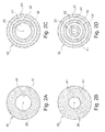
- Figure 2A-2D show possible arrangements of the hydrophilic and hydrophobic regions about the aperture 20.
- the first hydrophilic region 41 immediately surrounds said aperture 20 and the first hydrophobic region 51 is located radially outwards of, and surrounds, said first hydrophilic region 41. As such, the cell 120, when adhered to the chip 10 makes contact with both hydrophilic and hydrophobic regions.
- the outermost periphery of said cell adhesion region 30 consists of said first hydrophobic region 51. That is, the first hydrophobic region defines the outermost periphery of the cell adhesion region 30.
- the cell adhesion region 30 comprises three or more, such as three, four, five or six, alternating hydrophilic regions 41, 42, 43... and hydrophobic regions 51, 52, 53... arranged concentrically about the aperture 20 (e.g. Figure 2C and 2D ).
- the cell adhesion region 30 consists of at least one hydrophilic region 41, 42 and at least one hydrophobic region 51, 52. In other words, no other regions are present.
- the hydrophilic regions may have a total surface area which is at least 50% (50% in Fig. 2A ), preferably at least 75% (75% in Fig. 2B ) of the surface area of said cell adhesion region 30.
- XPS X-ray Photon Spectroscopy
- hydrophilic regions 41, 42 are created by surface modification of selected regions of the upper surface 15 within said cell adhesion region 30. Surface modification reduces the need for chip construction using separate materials. Most suitably, hydrophilic regions 41, 42 are created by surface modification of selected regions of the upper surface 15 when the material of the chip 10 is hydrophobic, thus readily creating hydrophobic and hydrophilic regions as required.
- the first hydrophilic region 41 surrounds the aperture 20, and may also extend into the aperture 20. Cell adhesion within the aperture and/or encroachment of the cell 120 into the aperture is thus improved.
- the present invention provides improved cell adhesion by varying the hydrophilicity/hydrophobicity of the upper surface 15 within the cell adhesion region according to a predetermined pattern. As such, a single cell 120 occupying the cell adhesion region 30 will make contact with both hydrophilic and hydrophobic regions in a given pattern.
- the chip 10 according to the present invention is applicable in: patch clamp analysis; other kinds of electrochemical analyses, in which a wet domain is separated from a dry domain; a coulter counter; flow cytometry; microfluidic analysis systems, wherein electrodes are provided on a single side of the chip 10, e.g. for the purpose of performing measurements on an immobilized or moving cell; miniature cantilever analysis for mass determination of e.g. single cells.
- One surface of the chip may, for example, comprise one or more components, which communicate with other components and/or with electronics on the other surface of the chip.
- an electrical or a fluid passage through the chip may communicate with one or more electrodes and/or measuring components at the first surface of the chip.
- the assembly according to the invention is useful as a measuring unit for measuring e.g. pressure, or as a cantilever mass sensor.
- the chip 10 of the invention may form part of a chip assembly 100, in which an array of chips 10 are located in a side-by-side arrangement.
- the material of the chip assembly 100 is the same as each individual chip 10 and is continuous between adjacent chips, so that the chip assembly consists of a plate of material with a plurality of apertures 20 and cell adhesion regions 30 located therein.
- the chips 10 of the present invention are assembled in a carrier structure as per co-pending application PCT/EP2011/061388 .
- the surface of the chip assembly 100 is suitably recessed in the cell adhesion regions 30, so that a plurality of wells is formed in the chip assembly 100.
- a chip assembly 100 consists of 8-400 chips 10.
- the invention also relates to a method for improving the adhesion of a cell 120 to a chip 10, said method comprising the steps of:
- the chip 10 according to the invention may be manufactured via a number of methods. However, a preferred method comprises the steps of:
- An aperture or hole is created by many 'applied shots' of laser energy known as pulses.
- the depth over which the laser energy is absorbed and therefore, the amount of material removed by a single laser pulse depends on the material's optical properties and the wavelength of the laser.
- the ablation rate R In order to drill holes into polymers, the ablation rate R , must be increased above an ablation threshold ⁇ ⁇ 1, which is logarithmic to the energy fluence, ⁇ (Beers Law)
- a laser source and mirrors reflect the light beam through a motorized quartz chrome mask (as used in traditional semi-conductor microlithography), through deflecting mirrors through an objective onto a positioning table where the sample part is placed.
- the exposure area is approx. 2x2 mm.
- the drilled holes have a diameter on the laser exit side of 1-5 ⁇ m to prevent the cell falling through the hole.
- the diameter of the hole on the laser entrance side should allow electrolyte penetration to the bottom of the cell.
- the hole should be conical.
- the laser entrance side diameters are between 5-9 ⁇ m on average.
- the holes are less conical in shape and show an entrance diameter of 5 ⁇ m and exit diameter of 3 ⁇ m. Increasing the energy fluence shows another behaviour than at 0.5mJ/cm 2 .
- the exit diameter is oval and at 1.5mJ/cm 2 the holes are round.
- modification of the upper surface 15 in step c. is carried out by irradiation of said upper surface 15, either by UV irradiation or laser irradiation. This can readily be achieved using the same or different lasers as used to create the aperture 20. Photomasking of certain regions of the chip 10 allows selective modification in the desired regions.
- Regions of the upper surface 15 may be modified by micro-lithography.
- Microlithography is the technology used in semiconductor manufacturing to image a pattern from a photomask onto a silicon wafer coated with a UV-light sensitive photoresist material.
- the photomask has a thin patterned chrome layer on the bottom which is nearly opaque to UV light wavelengths. UV light is passed through the photomask or reflected by the patterned chrome layer.
- the photoresist on the wafer is then exposed with the shadow pattern of the photomask and a blueprint is created in the resist forming the basic design of, for example, CMOS chips.
- photoresists There are two basic types of photoresists; positive or negative. When exposed to UV light, the bonds of a positive photoresist such as Clarient AZ4533 are scissioned where subjected to UV light. A salt solution can be used to rinse away broken bond material leaving unexposed photoresist structures behind. In simplified microlithography, a short wavelength lamp at ⁇ 200nm preferably at 185nm can be used to make hydrophilic surface modifications without the need for a photoresist. The photomask is aligned around the drilled hole and the UV light is used with a minimum dose of 1J/cm 2 to break the surface bonds of the polymer material, thus creating stable -COOH bonds.
- a positive photoresist such as Clarient AZ4533
- a salt solution can be used to rinse away broken bond material leaving unexposed photoresist structures behind.
- a short wavelength lamp at ⁇ 200nm preferably at 185nm can be used to make hydrophilic surface modifications without the need for
- a patterned surface modification which breaks covalent bonds can be made by using a step and repeat beam process.
- a laser beam moves across a surface at an energy fluence below the ablation threshold.
- the ablation threshold is determined experimentally by number of pulses, laser frequency and applied energy.
- the 193nm UV laser has the photonic energy sufficient to break covalent bonds such as in benzene, and ambient air reacts with the broken C-H bonds with the goal of creating more COOH groups.
- Laser surface modifications can be performed at 193nm using an ArF ATLEX laser (ATL Lasertechnik, Wermelsmün, Germany) at different energy fluencies, frequencies, and number of pulses and in ambient air.
- a chromium/quartz mask may also be used but as a projection mask not in contact with the material.
- the mask feature size demagnification factor to the final achieved feature size is 4:1.
- Laser modification is illustrated in Figure 4 .
- a foil of polystyrene is provided, the modification is by laser as described above, and then Dip Pen NanoLithography (DPNL) lipid rings are applied,
- the dashed grey circle indicated by (A) is a hydrophilic region.
- the three concentric rings indicated by (B), and the smaller central ring comprise (DPNL) lipid rings labelled with 5% Rhodamine.
- Arrow (C) indicates a laser exit hole (2 ⁇ m).
- modification of the upper surface 15 may be carried out by chemical deposition on the upper surface 15. Such a modification can also provide a hydrophobic region 51.
- Hozumi et al. Langmuir 2003, 19, 7573-7579 describes the formation of an oxide nanoskin on poly(methyl-methacrylate), thus forming hydrophilic regions on the substrate.
- an additive surface hydrophobicity can be carried out by lithographic processes whereby a layer of hydrophobic material (amorphous glass, amorphous polymer (such as fluoropolymers), semi-crystalline polymer such as polycaprolactone (PCL)) is patterned onto the surface by a lift off technique or by preferential surface affinity.
- a layer of hydrophobic material amorphous glass, amorphous polymer (such as fluoropolymers), semi-crystalline polymer such as polycaprolactone (PCL)
- the upper surface 15 of the chip precursor 11 is sufficiently hydrophobic in the region located radially outwards of, and surrounding said first hydrophilic region 41 (i.e. the first hydrophobic region 51), it can be left without modification. However, it is also possible to coat or otherwise modify this region so as to increase its hydrophobicity to a desired level.
- the portion of the cell adhesion region 30 which is not the first hydrophilic region 41 constitutes the first hydrophobic region 51.
- a droplet is placed on the substrate with dosing volume and rate, both variable, and recorded for a specific time by a CCD camera.
- a contact angle is determined for each individual photo taken.
- the dynamic contact angle is determined at between 5 and 15 seconds. Distilled water was used for these experiments with a surface energy of 72.8J/m (with a polar component of 51.1J/m and a dispersive component of 21.8J/m) (Gleich, 2004). Due to the interactions of the hydrogen bonds the polar component is larger than the dispersive component.
- a drop of approx. 2 ⁇ L was placed initially on the substrate and the pipette tip was positioned at the centre of the droplet and then water injected at a rate of 0.7 ⁇ L/s until a droplet volume of 16 ⁇ L was reached. Simultaneously the camera recorded this process with a speed of 16 photos per second for a total of 500 photos over a 20 second duration.
- X-ray photoelectron spectroscopy (XPS) measurements were carried out on an ESCALAB 5 spectrometer (Vacuum Generators, East Grinsted, UK) using non-monochromatized MgK ⁇ radiation (K ⁇ : 1253.6 eV) at a pressure of ⁇ 10 -9 mbar.
- the binding energy scale was referenced to 285.0 eV for the main C1s (C-H bond) feature.
- the base pressure in the analysis chamber was ⁇ 10 -10 mbar and increased to approx. 5x10 -8 mbar during measurement.
- the photoelectrons were detected at a take-off angle of 60° with respect to the normal of the sample surface. That means that the informational depth of the measurements is equal to or lower than 5nm.
- Exposed and unexposed reference foil materials are cut into 10x10 mm squares before placement into the measurement chamber.
- the preparation of SU-8 (a photo-sensitive epoxy resist) surfaces was somewhat more complex.
- a silicon wafer is laser engraved with a 10x10mm square matrix for easier sample sectioning after processing.
- SU-8 is spincoated onto a silicon substrate, soft baked at 95°C for 2 minutes, then the entire surface is flood exposed under UV light at 365nm (filtered) with an energy dose of 1000mJ/cm 2 , a post-exposure bake of 95°C for 5 minutes, then developed for 10 minutes in PGMEA, slowly rinsed with isopopanol, and allowed to air dry with the SU-8 layer facing downwards in a fumehood.
- a short oxygen plasma cleaning step (100W/5 mins) is performed after sample drying. The samples are separated into 10x10mm sections using gentle mechanical force before being placed into the measurement chamber.
- PS polystyrene
- PC polycarbonate
- LCP liquid crystal polymer
- the surfaces were analyzed using contact angle measurements and XPS to determine the surface chemistry, and roughness was measured using a contact profilometer (Tencor).
- Petri dishes show a ridge type structure if they are structured by UV laser above the ablation threshold.
- This ridge type structure is considered a material artefact as it cannot be altered by laser radiation density or number of pulses and is also independent of laser direction (parallel or perpendicular to the ridges).
- energy fluencies of 20mJ/cm 2 selective material removal occurs in the amorphous areas. Semi-crystalline areas have a higher removal rate leading to ridge-type structures.
- UV-lamp modification also leads to a logarithmic increase in oxygen stoichiometry as a function of exposure time T and total exposure dose E tot (figure 50).
- T time
- E tot 1.5 J/cm 2
- oxygen content reaches a value of about 34 at%.
- oxygen as processing gas a similar oxygen stoichiometry can be reached. This means that laser modification with 150 or 300 laser pulses leads to a polystyrene surface which is not fully oxidized, this agrees very well with the results which were obtained by contact angle measurements.
- the logarithmic increase in oxide layer thickness is typical for physisorption and subsequent chemisorption processes at the surface.
- the reaction zone is limited to the nanometer-scale and bulk diffusion of oxygen can be neglected.
- Cell attachment was analysed by coating the modified surfaces with cells under a 48h period, dyeing the cells and visually determining whether cells attached or not.
- the cell types used were L292 (murine fibroblast cells), HEPG2 (human hepatocellular liver carcinoma cells) and PC-12GFP (rat liver adrenal gland tumour cells).
Landscapes
- Health & Medical Sciences (AREA)
- Chemical & Material Sciences (AREA)
- Life Sciences & Earth Sciences (AREA)
- Engineering & Computer Science (AREA)
- Analytical Chemistry (AREA)
- General Health & Medical Sciences (AREA)
- Biomedical Technology (AREA)
- Physics & Mathematics (AREA)
- Hematology (AREA)
- Chemical Kinetics & Catalysis (AREA)
- Biochemistry (AREA)
- Clinical Laboratory Science (AREA)
- Molecular Biology (AREA)
- General Physics & Mathematics (AREA)
- Immunology (AREA)
- Pathology (AREA)
- Food Science & Technology (AREA)
- Biophysics (AREA)
- Urology & Nephrology (AREA)
- Medicinal Chemistry (AREA)
- Dispersion Chemistry (AREA)
- Electrochemistry (AREA)
- Apparatus Associated With Microorganisms And Enzymes (AREA)
- Micromachines (AREA)
- Investigating Or Analysing Biological Materials (AREA)
Description
- The present invention relates to a chip for use in a microfluidic analysis system, to the use thereof, and a method of manufacturing such a chip.
- The integration of sensor chips in carrier plates, also referred to as microtitre plates, is of particular concern of the present invention. Embodiments of the chip may provide a so-called lab-on-a-chip device, which integrates laboratory functions onto a single chip. An assembly of such chips, which may comprise an array of a plurality of chips on a single carrier, is applicable in a method for determining and/or monitoring electrophysiological properties of ion channels in ion channel-containing structures, typically lipid membrane-containing structures such as cells, by establishing an electrophysiological measuring configuration in which a cell membrane forms a high resistive seal around a measuring electrode, making it possible to determine and monitor a current flow through the cell membrane. The chip is for example useful in a method for analysing the electrophysiological properties of a cell membrane comprising a glycocalyx. The chip may be used in or form part of an apparatus for studying electrical events in cell membranes, such as an apparatus for carrying out patch clamp techniques utilised to study ion transfer channels in biological membranes.
- Microfluidic analyses of biological systems are widely used in medical and biological research in order to assess the mutual effects of various combinations of reagents and samples. So-called microtitre plates have been developed, which are flat plates with a plurality of wells used as small reactor chambers. Such microtitre plates have become a standard tool in analytical research and clinical diagnostic testing laboratories.
- In particular, with chips to be used in patch clamp techniques, good adhesion of the cell to the chip is required, so that a high-resistance seal can be obtained between the chip and the cell membrane (a "gigaseal").
-
US2002/0110847 describes a method for measuring a state variable of a biological cell. - S. Wilson et al. IEEE Sensors 2009 Conference, 1538-1541 describes novel processing for a patch clamp system.
- Pfleging et al, Proc. of SPIE Vol. 6880, 2008 _discloses patterning of polystyrene by UV laser radiation.
- Other microfluidic systems are described in
US2011/0083961 ,EP 2 037 258 ,US 2004/0146849 ,WO01/56771 WO02/16651 US2005/0279730 . - Despite efforts to date, the need remains for a chip having improved cell adhesion characteristics, which can be manufactured in a simple, effective manner.
- It is an object of the invention to provide a chip for use in a microfluidic analysis system, said chip having improved cell adhesion. A method for manufacture of the chips, and a method for improving the adhesion of a cell to a chip are also disclosed.
- It has been found by the present inventors that by providing a specific arrangement of hydrophobic and hydrophilic surfaces around the aperture of a patch clamp chip, cell adhesion is improved.
- Accordingly, the present invention relates to a chip for use in a microfluidic analysis system, such as a patch-clamp system. The chip has an upper surface and a central aperture located in said upper surface. The upper surface comprises a cell adhesion region surrounding the aperture. The cell adhesion region comprises three or more alternating hydrophilic and hydrophobic regions. A first hydrophilic region immediately surrounds said aperture and a first hydrophobic region is located radially outwards of, and surrounds, said first hydrophilic region.
- The invention also provides a method for improving the adhesion of a cell to a chip. The method comprises the steps of:
- a. providing a chip according to the invention;
- b. allowing said cell to make contact with the cell adhesion region of said chip, such that the entirety of said cell adhesion region is in contact with said cell, thereby providing improved adhesion of said cell to said chip.
- Additionally, a method for the manufacture of a chip according to the invention is provided. The method comprising the steps of:
- a. providing a chip precursor having an upper surface, said upper surface comprising a cell adhesion region and said upper surface being hydrophobic in at least said cell adhesion region;
- b. creating an aperture in said hydrophobic upper surface, located within said cell adhesion region;
- c. modifying the upper surface in a portion of the cell adhesion region, in at least one region immediately surrounding the aperture, so as to provide a first hydrophilic region;
- d. optionally, modifying the upper surface in a portion of the cell adhesion region, in at least one other region located radially outwards of, and surrounding said first hydrophilic region, so as to provide a first hydrophobic region.
- Further aspects of the invention are set out in the following description text, the enclosed Figures and the dependent claims.
- The invention will now be described with reference to the appended schematic figures, in which:
-
Figures 1A and1B are a cross-sectional views of a patch clamp device, with (1B) and without (1A) a cell in position. -
Figs. 2A-2D illustrate alternative arrangements of hydrophilic and hydrophobic regions -
Figure 3 illustrates a chip assembly according to the invention, in partial cut-away view. -
Figure 4 illustrates the result of laser surface modification of a polystyrene foil to become hydrophilic. - When a first element "surrounds" a second element in a given plane, it means that the first element extends completely about the entirety of the second element, without overlap and without interruption of either element. If a first element "immediately surrounds" a second element in a given plane, this means that there is no intervening region between said first and second elements - i.e. the first element is in contact with the second element about the entire periphery of the second element.
- The term "radial" defines a direction in the plane of the surface which is perpendicular to a line passing through the centre of the aperture in said surface. "Radially outwards" is a direction away from the aperture in the plane of the surface, while "radially inwards" is a direction towards the aperture in the plane of the surface.
- A material or surface is described as hydrophilic if it has a natural affinity to water. Hydrophilic polymers are defined as those which have a contact angle with water of less than 90°, preferably less than 80°, more preferably less than 75°, even more preferably less than 50° and most preferably less than 20°, measured with an advancing contact angle measurement, as described herein. Conversely, a material or surface is described as hydrophobic if it has a natural aversion to water. Hydrophobic polymers are defined as those which have a contact angle with water of more than 90°, preferably more than 120°, more preferably more than 135°, most preferably more than 150°.
-
Figure 1 shows a cross-sectional view of achip 10 according to the present invention, being a patch-clamp device, in which acell 120 is located on thechip 10. - The
chip 10 has substantially planar upper andlower surfaces chip 10, it is also called a "foil". - The material of the
chip 10 must be biocompatible, with a high dielectric constant low dielectric loss. The materials should be formable to a high surface finish (average surface roughness, Ra <0.5mm) and be capable of having apertures (through-holes) formed therein in an accurate, reproducible manner, similar to a glass pipette. The chip material should preferably be optically translucent, so that optical analysis techniques such as fluorescence can be carried out. - Suitable materials for the
chip 10 include silicon, polymers, pure silica and other glasses such as quartz and pyrex or silica, optionally doped with one or more dopants selected from the group of Be, Mg, Ca, B, Al, Ga, Ge, N, P, As. Polymers are preferred materials for thechip 10. Examples of polymers which are suitable are hydrophobic polymers such as polystyrene, polyimide, polypropylene and polyethylene. Liquid crystal polymers (LCP) are also useful polymers. Polystyrene is the most preferred material for thechip 10. - The
upper surface 15 of thechip 10 is preferably substantially planar. Thisupper surface 15 is configured to support a test item, e.g. an ion-channel containing structure, such as lipid membrane-containing structure, such as a cell, for electrochemical analysis thereof. The electrochemical analysis may hence take place while the test item is subjected to a fluid in contact with the item. It will accordingly be understood that the chip may be capable of conducting an electric current and/or capable of allowing ions to pass there through, e.g. through an orifice or aperture formed therein, so that an electrical connection may be established between two domains on either side of thechip 10. - The
chip 10 has acentral aperture 20 located in theupper surface 15. As shown inFigure 1 , theaperture 20 is a through-hole which provides a passage from the upper 15 to the lower 16 surface of thechip 10. - The
aperture 20 suitably has a circular cross-section, although other cross-sections are possible. The diameter of theaperture 20 at the upper surface is suitably 1-3µm. Theaperture 20 is preferably tapered, such that its diameter at thelower surface 16 is larger than its diameter at theupper surface 15. For instance, the diameter of theaperture 20 at the lower surface is suitably between 1.5 and 10µm. - Any suitable method for forming the
aperture 20 in thechip 10 may be used, depending on the material of thechip 10. The preferred method is excimer laser drilling using short pulse laser radiation (4nm). - Suction may be applied through the
aperture 20 to secure thecell 120 in place over the chip 10 (as perFigure 1A ). Electrodes (not shown) may be provided in both of the aforementioned domains in order to determine an electrical resistance, a flow of ions or a voltage difference across thecell 120 and through theaperture 20. - The
upper surface 15 of the chip comprises acell adhesion region 30 surrounding saidaperture 20. Thecell adhesion region 30 is the region of theupper surface 15 which is occupied by asingle cell 120. Typically, the cell adhesion region is circular, with a radius of between 2 and 25 micrometers, preferably between 5 and 15 micrometers, suitably less than 10 micrometers. - The
cell adhesion region 30 comprises at least onehydrophilic region hydrophobic region Figure 2A-2D show possible arrangements of the hydrophilic and hydrophobic regions about theaperture 20. - The first
hydrophilic region 41 immediately surrounds saidaperture 20 and the firsthydrophobic region 51 is located radially outwards of, and surrounds, said firsthydrophilic region 41. As such, thecell 120, when adhered to thechip 10 makes contact with both hydrophilic and hydrophobic regions. - Suitably, the outermost periphery of said
cell adhesion region 30 consists of said firsthydrophobic region 51. That is, the first hydrophobic region defines the outermost periphery of thecell adhesion region 30. - The
cell adhesion region 30 comprises three or more, such as three, four, five or six, alternatinghydrophilic regions hydrophobic regions Figure 2C and 2D ). - Suitably, the
cell adhesion region 30 consists of at least onehydrophilic region hydrophobic region - The hydrophilic regions may have a total surface area which is at least 50% (50% in
Fig. 2A ), preferably at least 75% (75% inFig. 2B ) of the surface area of saidcell adhesion region 30. - It has been discovered that the ratio of C-O bonds to C=O bonds in the hydrophilic region is also important. Suitably, therefore, the hydrophilic region(s) 41, 42 have a ratio of C-O bonds to C=O bonds of between 0.8:1 - 1:2.0, preferably 0.9:1 - 1:1.5, more preferably 1:1. This ratio is measured by X-ray Photon Spectroscopy (XPS), as set out below.
- In one aspect,
hydrophilic regions upper surface 15 within saidcell adhesion region 30. Surface modification reduces the need for chip construction using separate materials. Most suitably,hydrophilic regions upper surface 15 when the material of thechip 10 is hydrophobic, thus readily creating hydrophobic and hydrophilic regions as required. - The first
hydrophilic region 41 surrounds theaperture 20, and may also extend into theaperture 20. Cell adhesion within the aperture and/or encroachment of thecell 120 into the aperture is thus improved. - It has previously been thought that a simple change in the surface structure of the chip (e.g. from hydrophobic to hydrophilic) across the entire cell adhesion region would provide improved cell adhesion. However, the present invention provides improved cell adhesion by varying the hydrophilicity/hydrophobicity of the
upper surface 15 within the cell adhesion region according to a predetermined pattern. As such, asingle cell 120 occupying thecell adhesion region 30 will make contact with both hydrophilic and hydrophobic regions in a given pattern. - The
chip 10 according to the present invention is applicable in: patch clamp analysis; other kinds of electrochemical analyses, in which a wet domain is separated from a dry domain; a coulter counter; flow cytometry; microfluidic analysis systems, wherein electrodes are provided on a single side of thechip 10, e.g. for the purpose of performing measurements on an immobilized or moving cell; miniature cantilever analysis for mass determination of e.g. single cells. - One surface of the chip may, for example, comprise one or more components, which communicate with other components and/or with electronics on the other surface of the chip. For example, an electrical or a fluid passage through the chip may communicate with one or more electrodes and/or measuring components at the first surface of the chip. In such embodiment, the assembly according to the invention is useful as a measuring unit for measuring e.g. pressure, or as a cantilever mass sensor.
- The
chip 10 of the invention may form part of achip assembly 100, in which an array ofchips 10 are located in a side-by-side arrangement. Suitably, the material of thechip assembly 100 is the same as eachindividual chip 10 and is continuous between adjacent chips, so that the chip assembly consists of a plate of material with a plurality ofapertures 20 andcell adhesion regions 30 located therein. As an alternative, thechips 10 of the present invention are assembled in a carrier structure as per co-pending applicationPCT/EP2011/061388 - The surface of the
chip assembly 100 is suitably recessed in thecell adhesion regions 30, so that a plurality of wells is formed in thechip assembly 100. Typically, achip assembly 100 consists of 8-400chips 10. - The invention also relates to a method for improving the adhesion of a
cell 120 to achip 10, said method comprising the steps of: - a. providing a
chip 10 according to the invention; - b. allowing said cell to make contact with the
cell adhesion region 30 of saidchip 10, such that the entirety of saidcell adhesion region 30 is in contact with said cell, thereby providing improved adhesion of said cell to saidchip 10. - The
chip 10 according to the invention may be manufactured via a number of methods. However, a preferred method comprises the steps of: - a. providing a chip precursor 11 having an
upper surface 15, saidupper surface 15 comprising acell adhesion region 30 and saidupper surface 15 being hydrophobic in at least saidcell adhesion region 30; - b. creating an
aperture 20 in said hydrophobicupper surface 15, located within saidcell adhesion region 30; - c. modifying the
upper surface 15 in a portion of the cell adhesion region, in at least one region immediately surrounding theaperture 20, so as to provide a firsthydrophilic region 41; - d. optionally, modifying the
upper surface 15 in a portion of thecell adhesion region 30, in at least one other region located radially outwards of, and surrounding said firsthydrophilic region 41, so as to provide a firsthydrophobic region 51. - An aperture or hole is created by many 'applied shots' of laser energy known as pulses. The depth over which the laser energy is absorbed and therefore, the amount of material removed by a single laser pulse depends on the material's optical properties and the wavelength of the laser.
- Basic requirements must be met to structure polymers, such as a sufficient coefficient of absorption (αeff > 1µm -1) for the laser wavelength used (Cleve et al., 1999)
- In order to drill holes into polymers, the ablation rate R , must be increased above an ablation threshold ε ↓ 1, which is logarithmic to the energy fluence, ε (Beers Law)

- Very high energy densities and a fast dissolution of ablated fragments leads to a material vapour plasma. This plasma partially absorbs the laser radiation. This is the so-called saturation area (Pettit and Sauerbrey, 1993).
- In a laser setup at 193nm for hole ablation, a laser source and mirrors reflect the light beam through a motorized quartz chrome mask (as used in traditional semi-conductor microlithography), through deflecting mirrors through an objective onto a positioning table where the sample part is placed. The exposure area is approx. 2x2 mm.
- In terms of the influence of laser wavelength, a photochemical process happens at wavelengths <200nm as covalent bonds are broken and material is ablated if energy applied is above the ablation threshold. Volatile fragments are then dissolved. The photon energy for 193nm is 6.4 eV. It is above the bond energy for most covalent bonds (Laurens, 2000).
- At wavelengths >248nm and depending on material, the electronic excitation does not lead to a break in molecular chains. In this case, rapid heating occurs followed by an explosive evaporation (Pettit and Sauerbrey, 1993). For wavelengths >300nm single and multiple pulses lead to heating in the energy absorption ranges resulting in a thermal decomposition. A single pulse is insufficient to break covalent bonds (Pettit and Sauerbrey, 1993).
- The drilled holes have a diameter on the laser exit side of 1-5µm to prevent the cell falling through the hole. The diameter of the hole on the laser entrance side should allow electrolyte penetration to the bottom of the cell. Ideally, the hole should be conical. At a fluence of 0.5mJ/cm2 the best desired result was achieved. The cells sit on the exit side of the hole with a diameter of between 1 and 4 µm. For optimum penetration of cell culture medium, the laser entrance side diameters are between 5-9µm on average. At laser fluences of 0.8mJ/cm2 and 1.5mJ/cm2 the holes are less conical in shape and show an entrance diameter of 5µm and exit diameter of 3µm. Increasing the energy fluence shows another behaviour than at 0.5mJ/cm2. At 0.8mJ/cm2 the exit diameter is oval and at 1.5mJ/cm2 the holes are round.
- Suitably, modification of the
upper surface 15 in step c. is carried out by irradiation of saidupper surface 15, either by UV irradiation or laser irradiation. This can readily be achieved using the same or different lasers as used to create theaperture 20. Photomasking of certain regions of thechip 10 allows selective modification in the desired regions. - Regions of the
upper surface 15 may be modified by micro-lithography. Microlithography is the technology used in semiconductor manufacturing to image a pattern from a photomask onto a silicon wafer coated with a UV-light sensitive photoresist material. The photomask has a thin patterned chrome layer on the bottom which is nearly opaque to UV light wavelengths. UV light is passed through the photomask or reflected by the patterned chrome layer. The photoresist on the wafer is then exposed with the shadow pattern of the photomask and a blueprint is created in the resist forming the basic design of, for example, CMOS chips. - There are two basic types of photoresists; positive or negative. When exposed to UV light, the bonds of a positive photoresist such as Clarient AZ4533 are scissioned where subjected to UV light. A salt solution can be used to rinse away broken bond material leaving unexposed photoresist structures behind. In simplified microlithography, a short wavelength lamp at <200nm preferably at 185nm can be used to make hydrophilic surface modifications without the need for a photoresist. The photomask is aligned around the drilled hole and the UV light is used with a minimum dose of 1J/cm2 to break the surface bonds of the polymer material, thus creating stable -COOH bonds.
- With a negative photoresist, the reverse occurs. Areas exposed to UV light crosslink and remain on the substrate, while non-crosslinked areas are removed by an organic solvent.
- By remaining below the ablation threshold for polystyrene, a patterned surface modification which breaks covalent bonds can be made by using a step and repeat beam process. A laser beam moves across a surface at an energy fluence below the ablation threshold. The ablation threshold is determined experimentally by number of pulses, laser frequency and applied energy. As previously discussed, the 193nm UV laser has the photonic energy sufficient to break covalent bonds such as in benzene, and ambient air reacts with the broken C-H bonds with the goal of creating more COOH groups. By using a quartz chrome mask in the laser, and some reducing optics, very fine patterns can be 'written' into the surface of the material, and with optimized parameters no dry etching or ablation takes place.
- Laser surface modifications can be performed at 193nm using an ArF ATLEX laser (ATL Laser Technik, Wermelskirchen, Germany) at different energy fluencies, frequencies, and number of pulses and in ambient air. A chromium/quartz mask may also be used but as a projection mask not in contact with the material. The mask feature size demagnification factor to the final achieved feature size is 4:1.
- Laser modification is illustrated in
Figure 4 . In this example, a foil of polystyrene is provided, the modification is by laser as described above, and then Dip Pen NanoLithography (DPNL) lipid rings are applied, The dashed grey circle indicated by (A) is a hydrophilic region. The three concentric rings indicated by (B), and the smaller central ring comprise (DPNL) lipid rings labelled with 5% Rhodamine. Arrow (C) indicates a laser exit hole (2µm). - As an alternative to irradiation to produce hydrophilic surfaces, modification of the
upper surface 15 may be carried out by chemical deposition on theupper surface 15. Such a modification can also provide ahydrophobic region 51. For instance, Hozumi et al. Langmuir 2003, 19, 7573-7579 describes the formation of an oxide nanoskin on poly(methyl-methacrylate), thus forming hydrophilic regions on the substrate. - In addition to the native material surface hydrophobicity, an additive surface hydrophobicity can be carried out by lithographic processes whereby a layer of hydrophobic material (amorphous glass, amorphous polymer (such as fluoropolymers), semi-crystalline polymer such as polycaprolactone (PCL)) is patterned onto the surface by a lift off technique or by preferential surface affinity.
- Dip Pen Nanolithography. In test situations, a Langmuir Blodgett approach to depositing lipids onto hydrophobic surfaces has been attempted with either a single tip or in a multi-tip parallelised approach to produce hydrophobic patterns around a laser drilled. Other methods of applying Langmuir Blodgett types films (such as dipping, spin coating etc) could also be used.
- If the
upper surface 15 of the chip precursor 11 is sufficiently hydrophobic in the region located radially outwards of, and surrounding said first hydrophilic region 41 (i.e. the first hydrophobic region 51), it can be left without modification. However, it is also possible to coat or otherwise modify this region so as to increase its hydrophobicity to a desired level. - Suitably, the portion of the
cell adhesion region 30 which is not the firsthydrophilic region 41 constitutes the firsthydrophobic region 51. - All modified surfaces are analyzed by XPS and contact angle measurement in addition to cell adhesion.
- An
OCA 15 Plus goniometer from DataPhysics (Filderstadt, Germany) withSCA 20 software allows static and dynamic contact angle measurement. - For dynamic contact angle measurement a droplet is placed on the substrate with dosing volume and rate, both variable, and recorded for a specific time by a CCD camera. A contact angle is determined for each individual photo taken. The dynamic contact angle is determined at between 5 and 15 seconds. Distilled water was used for these experiments with a surface energy of 72.8J/m (with a polar component of 51.1J/m and a dispersive component of 21.8J/m) (Gleich, 2004). Due to the interactions of the hydrogen bonds the polar component is larger than the dispersive component.
- To measure the advancing contact angle a drop of approx. 2µL was placed initially on the substrate and the pipette tip was positioned at the centre of the droplet and then water injected at a rate of 0.7µL/s until a droplet volume of 16µL was reached. Simultaneously the camera recorded this process with a speed of 16 photos per second for a total of 500 photos over a 20 second duration.
- To measure the receding dynamic contact angle the reverse procedure was followed, the pipette tip was positioned in the middle of the droplet and water suctioned up at a rate of 0.7µL/s, an angle obtained and documented.
- Advancing and receding contact angle measurements were performed 5 times for each exposure dose and on different surface locations to ensure an average surface response and prevent already hydrated surfaces being re-measured. The front and back of the foils were measured to determine surface differences due to manufacture or chemistry.
- X-ray photoelectron spectroscopy (XPS) measurements were carried out on an ESCALAB 5 spectrometer (Vacuum Generators, East Grinsted, UK) using non-monochromatized MgKα radiation (Kα : 1253.6 eV) at a pressure of <10-9 mbar. The binding energy scale was referenced to 285.0 eV for the main C1s (C-H bond) feature. The base pressure in the analysis chamber was < 10-10 mbar and increased to approx. 5x10⁻⁸ mbar during measurement. The photoelectrons were detected at a take-off angle of 60° with respect to the normal of the sample surface. That means that the informational depth of the measurements is equal to or lower than 5nm.
- Exposed and unexposed reference foil materials are cut into 10x10 mm squares before placement into the measurement chamber. The preparation of SU-8 (a photo-sensitive epoxy resist) surfaces was somewhat more complex. A silicon wafer is laser engraved with a 10x10mm square matrix for easier sample sectioning after processing. SU-8 is spincoated onto a silicon substrate, soft baked at 95°C for 2 minutes, then the entire surface is flood exposed under UV light at 365nm (filtered) with an energy dose of 1000mJ/cm2, a post-exposure bake of 95°C for 5 minutes, then developed for 10 minutes in PGMEA, slowly rinsed with isopopanol, and allowed to air dry with the SU-8 layer facing downwards in a fumehood. A short oxygen plasma cleaning step (100W/5 mins) is performed after sample drying. The samples are separated into 10x10mm sections using gentle mechanical force before being placed into the measurement chamber.
- Surface modifications of polystyrene (PS), polycarbonate (PC) and liquid crystal polymer (LCP, from Rogers Corp., Chandler, Arizona, USA) were carried out using a UV lamp at 185nm. A quartz glass and chrome mask provided modified and unmodified regions. The lamp was positioned 10cm from the surface, and treatment was carried out for at least 30mins, providing 400milliwatts per cm2.
- The surfaces were analyzed using contact angle measurements and XPS to determine the surface chemistry, and roughness was measured using a contact profilometer (Tencor).
- Contact angle measurements were performed with an ambient humidity of between 38.8% and 49.4% and temperature ranges between 21.1° and 25°. As these variables are within a narrow range their influences on measurement are considered negligible.
- These processing influences can be highlighted particularly clearly using laser ablation. Petri dishes show a ridge type structure if they are structured by UV laser above the ablation threshold. This ridge type structure is considered a material artefact as it cannot be altered by laser radiation density or number of pulses and is also independent of laser direction (parallel or perpendicular to the ridges). For energy fluencies of 20mJ/cm2, selective material removal occurs in the amorphous areas. Semi-crystalline areas have a higher removal rate leading to ridge-type structures.
- A comparison of the effects of different laser pulse widths showed no significant difference in contact angle. Both 20ns and 4ns pulse widths only a very small difference was seen in contact angle hysteresis which can be considered negligible.
- Chemical analysis using XPS measurements show that for ε=4 mJ/cm2 the amount of oxygen on PS surfaces increases logarithmically with laser pulse number and total exposure dose. After 150 laser pulses (Etot=0.6 J/cm2) and even after 300 laser pulses (Etot=1.2 J/cm2) no difference between the used laser pulse lengths could be observed. After 150 laser pulses the amount of oxygen at the surface was 12at% and after 300 pulses the content of oxygen was 17-18 at%. For both laser pulse lengths and for UV-lamp assisted processing the C1s and O1s line shape of the modified polystyrene surface corresponds very well with the line shape of the chemical group -COOH.
- UV-lamp modification also leads to a logarithmic increase in oxygen stoichiometry as a function of exposure time T and total exposure dose Etot (figure 50). After long-term exposure (T=90 minutes, Etot=1.5 J/cm2) oxygen content reaches a value of about 34 at%. After 4000 laser pulses (Etot=16 J/cm2) and with oxygen as processing gas a similar oxygen stoichiometry can be reached. This means that laser modification with 150 or 300 laser pulses leads to a polystyrene surface which is not fully oxidized, this agrees very well with the results which were obtained by contact angle measurements.
- The logarithmic increase in oxide layer thickness is typical for physisorption and subsequent chemisorption processes at the surface. The reaction zone is limited to the nanometer-scale and bulk diffusion of oxygen can be neglected.
- The XPS measurements provided the following data (Table 1)
C-OH C=O Cell attachment PS 1 1 *** PC 1.5 1 * LCP 1 1 *** - Cell attachment was analysed by coating the modified surfaces with cells under a 48h period, dyeing the cells and visually determining whether cells attached or not. The cell types used were L292 (murine fibroblast cells), HEPG2 (human hepatocellular liver carcinoma cells) and PC-12GFP (rat liver adrenal gland tumour cells).
- Three stars (***) indicated good adhesion, while one star (*) indicated poor adhesion. It can be seen that a ratio of C-O bonds to C=O bonds in the hydrophilic regions of around 1:1 provides good cell attachment, which then weakens at a lower ratio.
- While the invention has been discussed in relation to a number of specific embodiments and examples, the scope thereof should not be considered as being limited to these embodiments and examples. Instead, the scope of the invention is defined in the appended claims.
Claims (14)
- A chip (10) for use in a microfluidic analysis system, said chip (10) having an upper surface (15) and a central aperture (20) located in said upper surface (15), said upper surface (15) comprising a cell adhesion region (30) surrounding said aperture (20), characterised in that said cell adhesion region (30) comprises three or more alternating hydrophilic and hydrophobic regions (41, 42, 51, 52) arranged concentrically about said aperture (20), wherein a first hydrophilic region (41) immediately surrounds said aperture (20) and wherein a first hydrophobic region (51) is located radially outwards of, and surrounds, said first hydrophilic region (41).
- A chip (10) according to claim 1, wherein the outermost periphery of said cell adhesion region (30) consists of said first hydrophobic region (51).
- A chip (10) according to any one of the preceding claims, wherein the cell adhesion region (30) comprises four, five or six, alternating hydrophilic and hydrophobic regions (41, 42, 51, 52) arranged concentrically about the aperture (20).
- A chip (10) according to any one of the preceding claims, wherein the hydrophobic regions have a combined surface area which is at least 50%, preferably at least 75% of the surface area of said cell adhesion region (30).
- A chip (10) according to any one of the preceding claims, wherein the cell adhesion region (30) consists of at least one hydrophilic region (41, 42) and at least one hydrophobic region (51, 52).
- A chip (10) according to any one of the preceding claims, wherein the cell adhesion region (30) is circular and has a radius of between 2 and 25 micrometers, preferably between 5 and 15 micrometers.
- A chip (10) according to any one of the preceding claims, wherein the hydrophilic region(s) (41, 42) have a ratio of C-O bonds to C=O bonds of between 0.8:1 - 1:2.0, preferably 0.9:1 - 1:1.5, more preferably 1:1.
- A chip (10) according to any one of the preceding claims, wherein hydrophilic regions (41, 42) are created by surface modification of selected regions of the upper surface (15) within said cell adhesion region (30).
- A chip (10) according to any one of the preceding claims, wherein the first hydrophilic region (41) extends into the aperture (20).
- A chip assembly (100) comprising a plurality of chips (10) according to any one of claims 1-9.
- A method for improving the adhesion of a cell to a chip (10), characterised in that said method comprises the steps of:a. providing a chip (10) according to any one of claims 1-9;b. allowing said cell to make contact with the cell adhesion region (30) of said chip (10), such that the entirety of said cell adhesion region (30) is in contact with said cell, thereby providing improved adhesion of said cell to said chip (10).
- A method for the manufacture of a chip (10) according to any one of claims 1-9, characterised in that said method comprises the steps of:a. providing a chip precursor (11) having an upper surface (15), said upper surface (15) comprising a cell adhesion region (30) and said upper surface (15) being hydrophobic in at least said cell adhesion region (30);b. creating an aperture (20) in said hydrophobic upper surface (15), located within said cell adhesion region (30);c. modifying the upper surface (15) in a portion of the cell adhesion region, in at least one region immediately surrounding the aperture (20), so as to provide a first hydrophilic region (41);d. optionally, modifying the upper surface (15) in a portion of the cell adhesion region (30), in at least one other region located radially outwards of, and surrounding said first hydrophilic region (41), so as to provide a first hydrophobic region (51).
- A method according to claim 12, wherein the modification in step c. is carried out by irradiation of the upper surface (15).
- A method according to claim 12, wherein the modification in step c. is carried out by chemical deposition on the upper surface (15).
Priority Applications (1)
| Application Number | Priority Date | Filing Date | Title |
|---|---|---|---|
| EP13700208.5A EP2802416B1 (en) | 2012-01-09 | 2013-01-08 | Improved patch area cell adhesion |
Applications Claiming Priority (4)
| Application Number | Priority Date | Filing Date | Title |
|---|---|---|---|
| US201261584427P | 2012-01-09 | 2012-01-09 | |
| EP12150459 | 2012-01-09 | ||
| EP13700208.5A EP2802416B1 (en) | 2012-01-09 | 2013-01-08 | Improved patch area cell adhesion |
| PCT/EP2013/050193 WO2013104608A1 (en) | 2012-01-09 | 2013-01-08 | Improved patch area cell adhesion |
Publications (2)
| Publication Number | Publication Date |
|---|---|
| EP2802416A1 EP2802416A1 (en) | 2014-11-19 |
| EP2802416B1 true EP2802416B1 (en) | 2016-04-06 |
Family
ID=48781068
Family Applications (1)
| Application Number | Title | Priority Date | Filing Date |
|---|---|---|---|
| EP13700208.5A Active EP2802416B1 (en) | 2012-01-09 | 2013-01-08 | Improved patch area cell adhesion |
Country Status (6)
| Country | Link |
|---|---|
| US (1) | US9649630B2 (en) |
| EP (1) | EP2802416B1 (en) |
| JP (1) | JP6290096B2 (en) |
| CA (1) | CA2860501C (en) |
| DK (1) | DK2802416T3 (en) |
| WO (1) | WO2013104608A1 (en) |
Cited By (2)
| Publication number | Priority date | Publication date | Assignee | Title |
|---|---|---|---|---|
| CN109718878A (en) * | 2019-01-08 | 2019-05-07 | 京东方科技集团股份有限公司 | The preparation method of pole plate, micro-fluidic chip and pole plate |
| WO2026077936A1 (en) * | 2024-10-09 | 2026-04-16 | Robert Bosch Gmbh | Microfluidic receiving element for a microfluidic device for biochemical processing of fluids |
Families Citing this family (2)
| Publication number | Priority date | Publication date | Assignee | Title |
|---|---|---|---|---|
| US10006882B2 (en) * | 2014-11-21 | 2018-06-26 | EnLiSense, LLC | Biosensing system and methods using electron-ionic mechanisms at fluid-sensor interfaces |
| JP7469092B2 (en) * | 2020-03-23 | 2024-04-16 | 株式会社Screenホールディングス | Cell Retention Container |
Family Cites Families (16)
| Publication number | Priority date | Publication date | Assignee | Title |
|---|---|---|---|---|
| US20020144905A1 (en) * | 1997-12-17 | 2002-10-10 | Christian Schmidt | Sample positioning and analysis system |
| EP1040349B2 (en) | 1997-12-17 | 2012-12-19 | Ecole Polytechnique Federale De Lausanne (Epfl) | Positioning and electrophysiological characterization of individual cells and reconstituted membrane systems on microstructured carriers |
| DE19841337C1 (en) | 1998-05-27 | 1999-09-23 | Micronas Intermetall Gmbh | Intracellular manipulation of biological cell contents, assisting injection or removal of substances or cell components |
| ATE317545T1 (en) | 1999-10-01 | 2006-02-15 | Sophion Bioscience As | ARRANGEMENT AND METHOD FOR DETERMINING AND/OR MONITORING ELECTROPHYSIOLOGICAL PROPERTIES OF ION CHANNELS |
| EP1218727A1 (en) | 1999-10-01 | 2002-07-03 | Fraunhofer-Gesellschaft Zur Förderung Der Angewandten Forschung E.V. | Method and device for determining substances such as e.g., dna sequences, in a sample |
| WO2001056771A2 (en) | 2000-01-31 | 2001-08-09 | Walter Schmidt | Method for fabricating micro-structures with various surface properties in multilayer body by plasma etching |
| US20020055111A1 (en) | 2000-08-25 | 2002-05-09 | Shiping Chen | Three-dimensional probe carriers |
| US7175980B2 (en) | 2000-10-30 | 2007-02-13 | Sru Biosystems, Inc. | Method of making a plastic colorimetric resonant biosensor device with liquid handling capabilities |
| US20040146849A1 (en) | 2002-01-24 | 2004-07-29 | Mingxian Huang | Biochips including ion transport detecting structures and methods of use |
| US20050009004A1 (en) * | 2002-05-04 | 2005-01-13 | Jia Xu | Apparatus including ion transport detecting structures and methods of use |
| US7919305B2 (en) | 2004-02-19 | 2011-04-05 | Dai Nippon Printing Co., Ltd. | Method for manufacturing cell culture substrate |
| EP1911078A1 (en) | 2005-07-25 | 2008-04-16 | Koninklijke Philips Electronics N.V. | Interconnection and packaging method for biomedical devices with electronic and fluid functions |
| DE102006033889A1 (en) | 2006-01-18 | 2007-09-20 | Evotec Technologies Gmbh | Microfluidic system and associated operating method |
| EP2037258A4 (en) | 2006-07-06 | 2013-12-04 | Panasonic Corp | DEVICE FOR ELECTROPHYSIOLOGICAL CELLULAR SENSOR, ELECTROPHYSIOLOGICAL CELL SENSOR USING THE DEVICE, AND METHOD FOR MANUFACTURING THE DEVICE FOR ELECTROPHYSIOLOGICAL CELLULAR SENSOR |
| US8835247B2 (en) | 2008-05-13 | 2014-09-16 | Nxp, B.V. | Sensor array and a method of manufacturing the same |
| WO2012004297A1 (en) | 2010-07-09 | 2012-01-12 | Sophion Bioscience A/S | A chip assembly for use in a microfluidic analysis system |
-
2013
- 2013-01-08 CA CA2860501A patent/CA2860501C/en active Active
- 2013-01-08 WO PCT/EP2013/050193 patent/WO2013104608A1/en not_active Ceased
- 2013-01-08 US US14/371,005 patent/US9649630B2/en active Active
- 2013-01-08 JP JP2014550717A patent/JP6290096B2/en active Active
- 2013-01-08 EP EP13700208.5A patent/EP2802416B1/en active Active
- 2013-01-08 DK DK13700208.5T patent/DK2802416T3/en active
Cited By (3)
| Publication number | Priority date | Publication date | Assignee | Title |
|---|---|---|---|---|
| CN109718878A (en) * | 2019-01-08 | 2019-05-07 | 京东方科技集团股份有限公司 | The preparation method of pole plate, micro-fluidic chip and pole plate |
| US11759778B2 (en) | 2019-01-08 | 2023-09-19 | Boe Technology Group Co., Ltd. | Electrode plate, microfluidic chip and method of manufacturing electrode plate |
| WO2026077936A1 (en) * | 2024-10-09 | 2026-04-16 | Robert Bosch Gmbh | Microfluidic receiving element for a microfluidic device for biochemical processing of fluids |
Also Published As
| Publication number | Publication date |
|---|---|
| DK2802416T3 (en) | 2016-07-04 |
| JP2015508997A (en) | 2015-03-26 |
| US20140353171A1 (en) | 2014-12-04 |
| JP6290096B2 (en) | 2018-03-07 |
| US9649630B2 (en) | 2017-05-16 |
| EP2802416A1 (en) | 2014-11-19 |
| WO2013104608A1 (en) | 2013-07-18 |
| CA2860501C (en) | 2021-05-18 |
| CA2860501A1 (en) | 2013-07-18 |
Similar Documents
| Publication | Publication Date | Title |
|---|---|---|
| Meredith et al. | Combinatorial materials science for polymer thin-film dewetting | |
| Hu et al. | Surface-directed, graft polymerization within microfluidic channels | |
| Stephan et al. | Fast prototyping using a dry film photoresist: microfabrication of soft-lithography masters for microfluidic structures | |
| US6020110A (en) | Production of electrodes for electrochemical sensing | |
| RU2360232C2 (en) | Colorimetric sensor | |
| JP3754337B2 (en) | Manufacturing method of resin molded product, manufacturing method of resin molded product and mold | |
| US9649630B2 (en) | Patch area cell adhesion | |
| WO2007126127A1 (en) | Cell culture container and method of producing the same | |
| EP3811078B1 (en) | A method and device for assaying the interaction and dynamics of permeation of a molecule and a lipid bilayer | |
| Bandara et al. | Patterned polycaprolactone-filled glass microfiber microfluidic devices for total protein content analysis | |
| US11906457B2 (en) | Light-activated gas sensor based on 3D nanostructure operable at low temperature with high performance and method for manufacturing the same | |
| US11280034B2 (en) | Nanofibrous carbon microstructures | |
| US20070202560A1 (en) | Resin microchannel array, method of manufacturing the same and blood test method using the same | |
| US20040228774A1 (en) | Microreactor, its production method, and sample screening device | |
| JP2005265634A (en) | Resin-made microchannel array, manufacturing method, and blood measurement method using the same | |
| Stevens et al. | Post arrays for the immobilization of vapochromic coordination polymers for chemical sensors | |
| Eray et al. | Highly stable bilayer lipid membranes (BLMs) formed on microfabricated polyimide apertures | |
| JP6061429B2 (en) | Method for manufacturing apparatus for detecting specimen | |
| Zheng et al. | Generation of chip based microelectrochemical cell arrays for long-term and high-resolution recording of ionic currents through ion channel proteins | |
| Støvring | Fabrication of pyrolytic carbon micro-and nanogap electrodes for electrochemical sensing | |
| Palinski et al. | Fast vapor detection by a micropillar array-integrated colorimetric sensor | |
| JP2003098069A (en) | Light transmissive plate for holding liquid and method of manufacturing the same | |
| Partel | Fabrication of interdigitated electrode arrays for biosensors by advanced mask aligner lithography | |
| Vandaveer IV | Analysis in small volumes with self-contained microcavity electrode devices | |
| KR20100048645A (en) | Method for microchannel fabrication by lift off technique |
Legal Events
| Date | Code | Title | Description |
|---|---|---|---|
| PUAI | Public reference made under article 153(3) epc to a published international application that has entered the european phase |
Free format text: ORIGINAL CODE: 0009012 |
|
| 17P | Request for examination filed |
Effective date: 20140811 |
|
| AK | Designated contracting states |
Kind code of ref document: A1 Designated state(s): AL AT BE BG CH CY CZ DE DK EE ES FI FR GB GR HR HU IE IS IT LI LT LU LV MC MK MT NL NO PL PT RO RS SE SI SK SM TR |
|
| DAX | Request for extension of the european patent (deleted) | ||
| RIC1 | Information provided on ipc code assigned before grant |
Ipc: G01N 27/327 20060101ALI20150820BHEP Ipc: G01N 33/487 20060101ALI20150820BHEP Ipc: B01L 3/00 20060101AFI20150820BHEP |
|
| GRAP | Despatch of communication of intention to grant a patent |
Free format text: ORIGINAL CODE: EPIDOSNIGR1 |
|
| INTG | Intention to grant announced |
Effective date: 20150928 |
|
| GRAS | Grant fee paid |
Free format text: ORIGINAL CODE: EPIDOSNIGR3 |
|
| GRAA | (expected) grant |
Free format text: ORIGINAL CODE: 0009210 |
|
| AK | Designated contracting states |
Kind code of ref document: B1 Designated state(s): AL AT BE BG CH CY CZ DE DK EE ES FI FR GB GR HR HU IE IS IT LI LT LU LV MC MK MT NL NO PL PT RO RS SE SI SK SM TR |
|
| REG | Reference to a national code |
Ref country code: GB Ref legal event code: FG4D |
|
| REG | Reference to a national code |
Ref country code: AT Ref legal event code: REF Ref document number: 787137 Country of ref document: AT Kind code of ref document: T Effective date: 20160415 Ref country code: CH Ref legal event code: EP |
|
| REG | Reference to a national code |
Ref country code: IE Ref legal event code: FG4D |
|
| REG | Reference to a national code |
Ref country code: DE Ref legal event code: R096 Ref document number: 602013006185 Country of ref document: DE |
|
| REG | Reference to a national code |
Ref country code: DK Ref legal event code: T3 Effective date: 20160624 |
|
| REG | Reference to a national code |
Ref country code: LT Ref legal event code: MG4D Ref country code: NL Ref legal event code: MP Effective date: 20160406 |
|
| REG | Reference to a national code |
Ref country code: AT Ref legal event code: MK05 Ref document number: 787137 Country of ref document: AT Kind code of ref document: T Effective date: 20160406 |
|
| PG25 | Lapsed in a contracting state [announced via postgrant information from national office to epo] |
Ref country code: NL Free format text: LAPSE BECAUSE OF FAILURE TO SUBMIT A TRANSLATION OF THE DESCRIPTION OR TO PAY THE FEE WITHIN THE PRESCRIBED TIME-LIMIT Effective date: 20160406 |
|
| PG25 | Lapsed in a contracting state [announced via postgrant information from national office to epo] |
Ref country code: PL Free format text: LAPSE BECAUSE OF FAILURE TO SUBMIT A TRANSLATION OF THE DESCRIPTION OR TO PAY THE FEE WITHIN THE PRESCRIBED TIME-LIMIT Effective date: 20160406 Ref country code: FI Free format text: LAPSE BECAUSE OF FAILURE TO SUBMIT A TRANSLATION OF THE DESCRIPTION OR TO PAY THE FEE WITHIN THE PRESCRIBED TIME-LIMIT Effective date: 20160406 Ref country code: LT Free format text: LAPSE BECAUSE OF FAILURE TO SUBMIT A TRANSLATION OF THE DESCRIPTION OR TO PAY THE FEE WITHIN THE PRESCRIBED TIME-LIMIT Effective date: 20160406 Ref country code: NO Free format text: LAPSE BECAUSE OF FAILURE TO SUBMIT A TRANSLATION OF THE DESCRIPTION OR TO PAY THE FEE WITHIN THE PRESCRIBED TIME-LIMIT Effective date: 20160706 Ref country code: IS Free format text: LAPSE BECAUSE OF FAILURE TO SUBMIT A TRANSLATION OF THE DESCRIPTION OR TO PAY THE FEE WITHIN THE PRESCRIBED TIME-LIMIT Effective date: 20160806 |
|
| PG25 | Lapsed in a contracting state [announced via postgrant information from national office to epo] |
Ref country code: LV Free format text: LAPSE BECAUSE OF FAILURE TO SUBMIT A TRANSLATION OF THE DESCRIPTION OR TO PAY THE FEE WITHIN THE PRESCRIBED TIME-LIMIT Effective date: 20160406 Ref country code: PT Free format text: LAPSE BECAUSE OF FAILURE TO SUBMIT A TRANSLATION OF THE DESCRIPTION OR TO PAY THE FEE WITHIN THE PRESCRIBED TIME-LIMIT Effective date: 20160808 Ref country code: GR Free format text: LAPSE BECAUSE OF FAILURE TO SUBMIT A TRANSLATION OF THE DESCRIPTION OR TO PAY THE FEE WITHIN THE PRESCRIBED TIME-LIMIT Effective date: 20160707 Ref country code: SE Free format text: LAPSE BECAUSE OF FAILURE TO SUBMIT A TRANSLATION OF THE DESCRIPTION OR TO PAY THE FEE WITHIN THE PRESCRIBED TIME-LIMIT Effective date: 20160406 Ref country code: ES Free format text: LAPSE BECAUSE OF FAILURE TO SUBMIT A TRANSLATION OF THE DESCRIPTION OR TO PAY THE FEE WITHIN THE PRESCRIBED TIME-LIMIT Effective date: 20160406 Ref country code: RS Free format text: LAPSE BECAUSE OF FAILURE TO SUBMIT A TRANSLATION OF THE DESCRIPTION OR TO PAY THE FEE WITHIN THE PRESCRIBED TIME-LIMIT Effective date: 20160406 Ref country code: AT Free format text: LAPSE BECAUSE OF FAILURE TO SUBMIT A TRANSLATION OF THE DESCRIPTION OR TO PAY THE FEE WITHIN THE PRESCRIBED TIME-LIMIT Effective date: 20160406 Ref country code: HR Free format text: LAPSE BECAUSE OF FAILURE TO SUBMIT A TRANSLATION OF THE DESCRIPTION OR TO PAY THE FEE WITHIN THE PRESCRIBED TIME-LIMIT Effective date: 20160406 |
|
| PG25 | Lapsed in a contracting state [announced via postgrant information from national office to epo] |
Ref country code: IT Free format text: LAPSE BECAUSE OF FAILURE TO SUBMIT A TRANSLATION OF THE DESCRIPTION OR TO PAY THE FEE WITHIN THE PRESCRIBED TIME-LIMIT Effective date: 20160406 Ref country code: BE Free format text: LAPSE BECAUSE OF FAILURE TO SUBMIT A TRANSLATION OF THE DESCRIPTION OR TO PAY THE FEE WITHIN THE PRESCRIBED TIME-LIMIT Effective date: 20160406 |
|
| REG | Reference to a national code |
Ref country code: DE Ref legal event code: R097 Ref document number: 602013006185 Country of ref document: DE |
|
| REG | Reference to a national code |
Ref country code: FR Ref legal event code: PLFP Year of fee payment: 5 |
|
| PG25 | Lapsed in a contracting state [announced via postgrant information from national office to epo] |
Ref country code: SK Free format text: LAPSE BECAUSE OF FAILURE TO SUBMIT A TRANSLATION OF THE DESCRIPTION OR TO PAY THE FEE WITHIN THE PRESCRIBED TIME-LIMIT Effective date: 20160406 Ref country code: RO Free format text: LAPSE BECAUSE OF FAILURE TO SUBMIT A TRANSLATION OF THE DESCRIPTION OR TO PAY THE FEE WITHIN THE PRESCRIBED TIME-LIMIT Effective date: 20160406 Ref country code: EE Free format text: LAPSE BECAUSE OF FAILURE TO SUBMIT A TRANSLATION OF THE DESCRIPTION OR TO PAY THE FEE WITHIN THE PRESCRIBED TIME-LIMIT Effective date: 20160406 Ref country code: CZ Free format text: LAPSE BECAUSE OF FAILURE TO SUBMIT A TRANSLATION OF THE DESCRIPTION OR TO PAY THE FEE WITHIN THE PRESCRIBED TIME-LIMIT Effective date: 20160406 |
|
| PLBE | No opposition filed within time limit |
Free format text: ORIGINAL CODE: 0009261 |
|
| STAA | Information on the status of an ep patent application or granted ep patent |
Free format text: STATUS: NO OPPOSITION FILED WITHIN TIME LIMIT |
|
| PG25 | Lapsed in a contracting state [announced via postgrant information from national office to epo] |
Ref country code: SM Free format text: LAPSE BECAUSE OF FAILURE TO SUBMIT A TRANSLATION OF THE DESCRIPTION OR TO PAY THE FEE WITHIN THE PRESCRIBED TIME-LIMIT Effective date: 20160406 |
|
| 26N | No opposition filed |
Effective date: 20170110 |
|
| PG25 | Lapsed in a contracting state [announced via postgrant information from national office to epo] |
Ref country code: SI Free format text: LAPSE BECAUSE OF FAILURE TO SUBMIT A TRANSLATION OF THE DESCRIPTION OR TO PAY THE FEE WITHIN THE PRESCRIBED TIME-LIMIT Effective date: 20160406 |
|
| REG | Reference to a national code |
Ref country code: CH Ref legal event code: PL |
|
| PG25 | Lapsed in a contracting state [announced via postgrant information from national office to epo] |
Ref country code: MC Free format text: LAPSE BECAUSE OF FAILURE TO SUBMIT A TRANSLATION OF THE DESCRIPTION OR TO PAY THE FEE WITHIN THE PRESCRIBED TIME-LIMIT Effective date: 20160406 |
|
| PG25 | Lapsed in a contracting state [announced via postgrant information from national office to epo] |
Ref country code: LI Free format text: LAPSE BECAUSE OF NON-PAYMENT OF DUE FEES Effective date: 20170131 Ref country code: CH Free format text: LAPSE BECAUSE OF NON-PAYMENT OF DUE FEES Effective date: 20170131 |
|
| REG | Reference to a national code |
Ref country code: IE Ref legal event code: MM4A |
|
| PG25 | Lapsed in a contracting state [announced via postgrant information from national office to epo] |
Ref country code: LU Free format text: LAPSE BECAUSE OF NON-PAYMENT OF DUE FEES Effective date: 20170108 |
|
| REG | Reference to a national code |
Ref country code: FR Ref legal event code: PLFP Year of fee payment: 6 |
|
| PG25 | Lapsed in a contracting state [announced via postgrant information from national office to epo] |
Ref country code: IE Free format text: LAPSE BECAUSE OF NON-PAYMENT OF DUE FEES Effective date: 20170108 |
|
| PG25 | Lapsed in a contracting state [announced via postgrant information from national office to epo] |
Ref country code: MT Free format text: LAPSE BECAUSE OF NON-PAYMENT OF DUE FEES Effective date: 20170108 |
|
| PG25 | Lapsed in a contracting state [announced via postgrant information from national office to epo] |
Ref country code: AL Free format text: LAPSE BECAUSE OF FAILURE TO SUBMIT A TRANSLATION OF THE DESCRIPTION OR TO PAY THE FEE WITHIN THE PRESCRIBED TIME-LIMIT Effective date: 20160406 |
|
| PG25 | Lapsed in a contracting state [announced via postgrant information from national office to epo] |
Ref country code: HU Free format text: LAPSE BECAUSE OF FAILURE TO SUBMIT A TRANSLATION OF THE DESCRIPTION OR TO PAY THE FEE WITHIN THE PRESCRIBED TIME-LIMIT; INVALID AB INITIO Effective date: 20130108 |
|
| PG25 | Lapsed in a contracting state [announced via postgrant information from national office to epo] |
Ref country code: BG Free format text: LAPSE BECAUSE OF FAILURE TO SUBMIT A TRANSLATION OF THE DESCRIPTION OR TO PAY THE FEE WITHIN THE PRESCRIBED TIME-LIMIT Effective date: 20160406 |
|
| PG25 | Lapsed in a contracting state [announced via postgrant information from national office to epo] |
Ref country code: CY Free format text: LAPSE BECAUSE OF FAILURE TO SUBMIT A TRANSLATION OF THE DESCRIPTION OR TO PAY THE FEE WITHIN THE PRESCRIBED TIME-LIMIT Effective date: 20160406 |
|
| PG25 | Lapsed in a contracting state [announced via postgrant information from national office to epo] |
Ref country code: MK Free format text: LAPSE BECAUSE OF FAILURE TO SUBMIT A TRANSLATION OF THE DESCRIPTION OR TO PAY THE FEE WITHIN THE PRESCRIBED TIME-LIMIT Effective date: 20160406 |
|
| PG25 | Lapsed in a contracting state [announced via postgrant information from national office to epo] |
Ref country code: TR Free format text: LAPSE BECAUSE OF FAILURE TO SUBMIT A TRANSLATION OF THE DESCRIPTION OR TO PAY THE FEE WITHIN THE PRESCRIBED TIME-LIMIT Effective date: 20160406 |
|
| PGFP | Annual fee paid to national office [announced via postgrant information from national office to epo] |
Ref country code: DK Payment date: 20251223 Year of fee payment: 14 |
|
| PGFP | Annual fee paid to national office [announced via postgrant information from national office to epo] |
Ref country code: GB Payment date: 20260113 Year of fee payment: 14 |
|
| PGFP | Annual fee paid to national office [announced via postgrant information from national office to epo] |
Ref country code: DE Payment date: 20260108 Year of fee payment: 14 |
|
| PGFP | Annual fee paid to national office [announced via postgrant information from national office to epo] |
Ref country code: FR Payment date: 20260113 Year of fee payment: 14 |