EP2802002B1 - Method for the manufacturing of a substrate having a hetero-structure - Google Patents
Method for the manufacturing of a substrate having a hetero-structure Download PDFInfo
- Publication number
- EP2802002B1 EP2802002B1 EP13195283.0A EP13195283A EP2802002B1 EP 2802002 B1 EP2802002 B1 EP 2802002B1 EP 13195283 A EP13195283 A EP 13195283A EP 2802002 B1 EP2802002 B1 EP 2802002B1
- Authority
- EP
- European Patent Office
- Prior art keywords
- metal
- substrate
- layer
- semiconductor layer
- semiconductor
- Prior art date
- Legal status (The legal status is an assumption and is not a legal conclusion. Google has not performed a legal analysis and makes no representation as to the accuracy of the status listed.)
- Active
Links
Images


Classifications
-
- H—ELECTRICITY
- H10—SEMICONDUCTOR DEVICES; ELECTRIC SOLID-STATE DEVICES NOT OTHERWISE PROVIDED FOR
- H10H—INORGANIC LIGHT-EMITTING SEMICONDUCTOR DEVICES HAVING POTENTIAL BARRIERS
- H10H20/00—Individual inorganic light-emitting semiconductor devices having potential barriers, e.g. light-emitting diodes [LED]
- H10H20/80—Constructional details
- H10H20/81—Bodies
- H10H20/815—Bodies having stress relaxation structures, e.g. buffer layers
-
- H—ELECTRICITY
- H10—SEMICONDUCTOR DEVICES; ELECTRIC SOLID-STATE DEVICES NOT OTHERWISE PROVIDED FOR
- H10D—INORGANIC ELECTRIC SEMICONDUCTOR DEVICES
- H10D62/00—Semiconductor bodies, or regions thereof, of devices having potential barriers
- H10D62/10—Shapes, relative sizes or dispositions of the regions of the semiconductor bodies; Shapes of the semiconductor bodies
- H10D62/124—Shapes, relative sizes or dispositions of the regions of semiconductor bodies or of junctions between the regions
- H10D62/125—Shapes of junctions between the regions
-
- H—ELECTRICITY
- H10—SEMICONDUCTOR DEVICES; ELECTRIC SOLID-STATE DEVICES NOT OTHERWISE PROVIDED FOR
- H10D—INORGANIC ELECTRIC SEMICONDUCTOR DEVICES
- H10D62/00—Semiconductor bodies, or regions thereof, of devices having potential barriers
- H10D62/80—Semiconductor bodies, or regions thereof, of devices having potential barriers characterised by the materials
- H10D62/82—Heterojunctions
- H10D62/824—Heterojunctions comprising only Group III-V materials heterojunctions, e.g. GaN/AlGaN heterojunctions
-
- H—ELECTRICITY
- H10—SEMICONDUCTOR DEVICES; ELECTRIC SOLID-STATE DEVICES NOT OTHERWISE PROVIDED FOR
- H10H—INORGANIC LIGHT-EMITTING SEMICONDUCTOR DEVICES HAVING POTENTIAL BARRIERS
- H10H20/00—Individual inorganic light-emitting semiconductor devices having potential barriers, e.g. light-emitting diodes [LED]
- H10H20/80—Constructional details
- H10H20/81—Bodies
- H10H20/819—Bodies characterised by their shape, e.g. curved or truncated substrates
- H10H20/82—Roughened surfaces, e.g. at the interface between epitaxial layers
-
- H—ELECTRICITY
- H10—SEMICONDUCTOR DEVICES; ELECTRIC SOLID-STATE DEVICES NOT OTHERWISE PROVIDED FOR
- H10H—INORGANIC LIGHT-EMITTING SEMICONDUCTOR DEVICES HAVING POTENTIAL BARRIERS
- H10H20/00—Individual inorganic light-emitting semiconductor devices having potential barriers, e.g. light-emitting diodes [LED]
- H10H20/80—Constructional details
- H10H20/81—Bodies
- H10H20/8215—Bodies characterised by crystalline imperfections, e.g. dislocations; characterised by the distribution of dopants, e.g. delta-doping
-
- H—ELECTRICITY
- H10—SEMICONDUCTOR DEVICES; ELECTRIC SOLID-STATE DEVICES NOT OTHERWISE PROVIDED FOR
- H10P—GENERIC PROCESSES OR APPARATUS FOR THE MANUFACTURE OR TREATMENT OF DEVICES COVERED BY CLASS H10
- H10P14/00—Formation of materials, e.g. in the shape of layers or pillars
- H10P14/20—Formation of materials, e.g. in the shape of layers or pillars of semiconductor materials
- H10P14/203—Formation of materials, e.g. in the shape of layers or pillars of semiconductor materials using transformation of metal, e.g. oxidation or nitridation
-
- H—ELECTRICITY
- H10—SEMICONDUCTOR DEVICES; ELECTRIC SOLID-STATE DEVICES NOT OTHERWISE PROVIDED FOR
- H10P—GENERIC PROCESSES OR APPARATUS FOR THE MANUFACTURE OR TREATMENT OF DEVICES COVERED BY CLASS H10
- H10P14/00—Formation of materials, e.g. in the shape of layers or pillars
- H10P14/20—Formation of materials, e.g. in the shape of layers or pillars of semiconductor materials
- H10P14/27—Formation of materials, e.g. in the shape of layers or pillars of semiconductor materials using selective deposition, e.g. simultaneous growth of monocrystalline and non-monocrystalline semiconductor materials
- H10P14/271—Formation of materials, e.g. in the shape of layers or pillars of semiconductor materials using selective deposition, e.g. simultaneous growth of monocrystalline and non-monocrystalline semiconductor materials characterised by the preparation of substrate for selective deposition
- H10P14/272—Formation of materials, e.g. in the shape of layers or pillars of semiconductor materials using selective deposition, e.g. simultaneous growth of monocrystalline and non-monocrystalline semiconductor materials characterised by the preparation of substrate for selective deposition using mask materials other than SiO2 or SiN
-
- H—ELECTRICITY
- H10—SEMICONDUCTOR DEVICES; ELECTRIC SOLID-STATE DEVICES NOT OTHERWISE PROVIDED FOR
- H10P—GENERIC PROCESSES OR APPARATUS FOR THE MANUFACTURE OR TREATMENT OF DEVICES COVERED BY CLASS H10
- H10P14/00—Formation of materials, e.g. in the shape of layers or pillars
- H10P14/20—Formation of materials, e.g. in the shape of layers or pillars of semiconductor materials
- H10P14/29—Formation of materials, e.g. in the shape of layers or pillars of semiconductor materials characterised by the substrates
- H10P14/2901—Materials
- H10P14/2902—Materials being Group IVA materials
- H10P14/2905—Silicon, silicon germanium or germanium
-
- H—ELECTRICITY
- H10—SEMICONDUCTOR DEVICES; ELECTRIC SOLID-STATE DEVICES NOT OTHERWISE PROVIDED FOR
- H10P—GENERIC PROCESSES OR APPARATUS FOR THE MANUFACTURE OR TREATMENT OF DEVICES COVERED BY CLASS H10
- H10P14/00—Formation of materials, e.g. in the shape of layers or pillars
- H10P14/20—Formation of materials, e.g. in the shape of layers or pillars of semiconductor materials
- H10P14/29—Formation of materials, e.g. in the shape of layers or pillars of semiconductor materials characterised by the substrates
- H10P14/2901—Materials
- H10P14/2921—Materials being crystalline insulating materials
-
- H—ELECTRICITY
- H10—SEMICONDUCTOR DEVICES; ELECTRIC SOLID-STATE DEVICES NOT OTHERWISE PROVIDED FOR
- H10P—GENERIC PROCESSES OR APPARATUS FOR THE MANUFACTURE OR TREATMENT OF DEVICES COVERED BY CLASS H10
- H10P14/00—Formation of materials, e.g. in the shape of layers or pillars
- H10P14/20—Formation of materials, e.g. in the shape of layers or pillars of semiconductor materials
- H10P14/32—Formation of materials, e.g. in the shape of layers or pillars of semiconductor materials characterised by intermediate layers between substrates and deposited layers
- H10P14/3202—Materials thereof
- H10P14/3214—Materials thereof being Group IIIA-VA semiconductors
- H10P14/3216—Nitrides
-
- H—ELECTRICITY
- H10—SEMICONDUCTOR DEVICES; ELECTRIC SOLID-STATE DEVICES NOT OTHERWISE PROVIDED FOR
- H10P—GENERIC PROCESSES OR APPARATUS FOR THE MANUFACTURE OR TREATMENT OF DEVICES COVERED BY CLASS H10
- H10P14/00—Formation of materials, e.g. in the shape of layers or pillars
- H10P14/20—Formation of materials, e.g. in the shape of layers or pillars of semiconductor materials
- H10P14/32—Formation of materials, e.g. in the shape of layers or pillars of semiconductor materials characterised by intermediate layers between substrates and deposited layers
- H10P14/3202—Materials thereof
- H10P14/3241—Materials thereof being conductive materials
-
- H—ELECTRICITY
- H10—SEMICONDUCTOR DEVICES; ELECTRIC SOLID-STATE DEVICES NOT OTHERWISE PROVIDED FOR
- H10P—GENERIC PROCESSES OR APPARATUS FOR THE MANUFACTURE OR TREATMENT OF DEVICES COVERED BY CLASS H10
- H10P14/00—Formation of materials, e.g. in the shape of layers or pillars
- H10P14/20—Formation of materials, e.g. in the shape of layers or pillars of semiconductor materials
- H10P14/32—Formation of materials, e.g. in the shape of layers or pillars of semiconductor materials characterised by intermediate layers between substrates and deposited layers
- H10P14/3242—Structure
- H10P14/3244—Layer structure
- H10P14/3251—Layer structure consisting of three or more layers
-
- H—ELECTRICITY
- H10—SEMICONDUCTOR DEVICES; ELECTRIC SOLID-STATE DEVICES NOT OTHERWISE PROVIDED FOR
- H10P—GENERIC PROCESSES OR APPARATUS FOR THE MANUFACTURE OR TREATMENT OF DEVICES COVERED BY CLASS H10
- H10P14/00—Formation of materials, e.g. in the shape of layers or pillars
- H10P14/20—Formation of materials, e.g. in the shape of layers or pillars of semiconductor materials
- H10P14/32—Formation of materials, e.g. in the shape of layers or pillars of semiconductor materials characterised by intermediate layers between substrates and deposited layers
- H10P14/3242—Structure
- H10P14/3256—Microstructure
-
- H—ELECTRICITY
- H10—SEMICONDUCTOR DEVICES; ELECTRIC SOLID-STATE DEVICES NOT OTHERWISE PROVIDED FOR
- H10P—GENERIC PROCESSES OR APPARATUS FOR THE MANUFACTURE OR TREATMENT OF DEVICES COVERED BY CLASS H10
- H10P14/00—Formation of materials, e.g. in the shape of layers or pillars
- H10P14/20—Formation of materials, e.g. in the shape of layers or pillars of semiconductor materials
- H10P14/34—Deposited materials, e.g. layers
- H10P14/3402—Deposited materials, e.g. layers characterised by the chemical composition
- H10P14/3414—Deposited materials, e.g. layers characterised by the chemical composition being group IIIA-VIA materials
- H10P14/3416—Nitrides
-
- H—ELECTRICITY
- H10—SEMICONDUCTOR DEVICES; ELECTRIC SOLID-STATE DEVICES NOT OTHERWISE PROVIDED FOR
- H10P—GENERIC PROCESSES OR APPARATUS FOR THE MANUFACTURE OR TREATMENT OF DEVICES COVERED BY CLASS H10
- H10P14/00—Formation of materials, e.g. in the shape of layers or pillars
- H10P14/20—Formation of materials, e.g. in the shape of layers or pillars of semiconductor materials
- H10P14/36—Formation of materials, e.g. in the shape of layers or pillars of semiconductor materials characterised by treatments done before the formation of the materials
-
- H—ELECTRICITY
- H10—SEMICONDUCTOR DEVICES; ELECTRIC SOLID-STATE DEVICES NOT OTHERWISE PROVIDED FOR
- H10H—INORGANIC LIGHT-EMITTING SEMICONDUCTOR DEVICES HAVING POTENTIAL BARRIERS
- H10H20/00—Individual inorganic light-emitting semiconductor devices having potential barriers, e.g. light-emitting diodes [LED]
- H10H20/01—Manufacture or treatment
- H10H20/011—Manufacture or treatment of bodies, e.g. forming semiconductor layers
- H10H20/013—Manufacture or treatment of bodies, e.g. forming semiconductor layers having light-emitting regions comprising only Group III-V materials
- H10H20/0137—Manufacture or treatment of bodies, e.g. forming semiconductor layers having light-emitting regions comprising only Group III-V materials the light-emitting regions comprising nitride materials
-
- H—ELECTRICITY
- H10—SEMICONDUCTOR DEVICES; ELECTRIC SOLID-STATE DEVICES NOT OTHERWISE PROVIDED FOR
- H10H—INORGANIC LIGHT-EMITTING SEMICONDUCTOR DEVICES HAVING POTENTIAL BARRIERS
- H10H20/00—Individual inorganic light-emitting semiconductor devices having potential barriers, e.g. light-emitting diodes [LED]
- H10H20/01—Manufacture or treatment
- H10H20/011—Manufacture or treatment of bodies, e.g. forming semiconductor layers
- H10H20/018—Bonding of wafers
Definitions
- the present invention relates to a method for manufacturing a nitride semiconductor, and more specifically, to a substrate having a hetero-structure (hereinafter, referred to simply as a "hetero-substrate").
- a light emitting device represented by a light emitting diode (LED) provides various colors through a p-n junction diode which converts electrical energy into light energy by controlling a compositional ratio of a compound semiconductor produced using a compound of Group III and V elements on the periodic table.
- LED light emitting diode
- Nitride semiconductors have attracted much attention in the field of development of optical devices and high-power electronic elements due to high thermal stability and wide band-gap energy thereof.
- blue light emitting devices, green light emitting devices, UV light emitting devices and the like using nitride semiconductors are commercialized and have entered widespread use.
- the light emitting device using such a nitride semiconductor may be implemented on a hetero-substrate made of materials such as sapphire or silicon carbide (SiC).
- nitride semiconductor thin films having a hetero-junction are grown using a sapphire substrate or other hetero-substrates or the like, differences in lattice mismatch and coefficient of thermal expansion caused by the hetero-junction may cause high crystal defects and high strain in thin films.
- the nitride semiconductor thin films grown on a sapphire substrate development of low-temperature gallium nitride (GaN) and low-temperature aluminum nitride (AlN) buffers and the like have been investigated in order to reduce dislocation generated on the substrate, such that defect density is reduced to some extent.
- the nitride semiconductor thin films still have a high defect density of about 108 cm -2 .
- GaN substrates have technical problems hindering commercialization, and entail cost several tens to several hundred times the cost of hetero-substrates, such as sapphire or Si, in terms of economic efficiency, thus restricting widespread use of GaN as a substrate.
- US 2004/067648 A1 relates to a crystal foundation having dislocations to obtain a crystal film of low dislocation density, a crystal substrate, and a semiconductor device.
- One side of a growth substrate is provided with a crystal layer with a buffer layer in between.
- the crystal layer has spaces in an end of each threading dislocation D1 elongating from below.
- the threading dislocation D1 is separated from the upper layer by the spaces so that each threading dislocation D1 is blocked from propagating to the upper layer.
- the upper layer above the spaces turns crystalline with a low dislocation density.
- US 2006/205197 A1 relates to a semiconductor device and method of manufacturing the same.
- the method includes coating a plurality of spherical balls on a substrate and selectively growing a compound semiconductor thin film on the substrate on which the spherical balls are coated.
- US 2009/008652 A1 relates to a free-standing substrate, a method for producing the same and a semiconductor light-emitting device.
- the free-standing substrate comprises a semiconductor layer and inorganic particles, wherein the inorganic particles are included in the semiconductor layer.
- the method for producing a free-standing substrate comprises the steps of: (a) placing inorganic particles on a substrate, (b) growing a semiconductor layer thereon, and (c) separating the semiconductor layer from the substrate, in that order.
- the semiconductor light-emitting device comprises the free-standing substrate, a conductive layer, a light-emitting device, and electrodes.
- the present invention is directed to a method for manufacturing substrate having a hetero-structure.
- a hetero-substrate includes a base substrate, a buffer layer disposed on the base substrate, a first semiconductor layer disposed on the buffer layer, the first semiconductor layer including a nitride semiconductor, a defect blocking layer disposed on the first semiconductor layer, the defect blocking layer including a plurality of metal droplets, and a second semiconductor layer disposed on the defect blocking layer, the second semiconductor layer including a nitride semiconductor.
- a method for manufacturing a hetero-substrate includes forming a buffer layer on a base substrate, forming a first semiconductor layer that includes a nitride semiconductor on the buffer layer, etching a surface of the first semiconductor layer to form a plurality of dislocation etch pits, forming a defect blocking layer that includes a plurality of metal droplets on the etched surface of the first semiconductor layer, subjecting a surface of the first semiconductor layer provided with the defect blocking layer to nitridation, and forming a second semiconductor layer that includes a nitride semiconductor on the defect blocking layer.
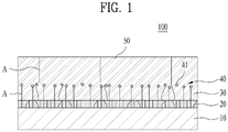
- FIG. 1 shows an example of a hetero-substrate 100 useful for the understanding of the inventive manufacturing method.
- a hetero-substrate or hetero-structure as used herein may refer to a semiconductor having multiple layers.
- the hetero-substrate 100 may include a base substrate 10.
- the base substrate 10 may be a sapphire or silicon (Si) substrate, but is not limited thereto.
- a buffer layer 20 is disposed on the base substrate 10.
- the buffer layer 20 may include a nucleation layer that enables formation of a nitride semiconductor by hetero-junction on a substrate.
- the substrate may be a substrate other than a nitride semiconductor substrate, such as a sapphire or silicon (Si) substrate.
- the buffer layer 20 may also serve as the nucleation layer.
- a first semiconductor layer 30 that includes a nitride semiconductor is disposed on the buffer layer 20.
- the nitride semiconductor may be a semiconductor containing nitride such as gallium nitride (GaN), aluminum nitride (AlN), aluminum gallium nitride (AlGaN), indium gallium nitride (InGaN), or another appropriate type of material.
- a defect blocking layer 40 that includes a plurality of metal droplets 41 is disposed on the first semiconductor layer 30.
- the metal droplets 41 are made of a mixture of two or more metal materials.
- a second metal 42 of a second type is disposed on a first metal 43 of a first type (see, for example, Figure 6 ).
- the first metal 43 is coated with the second metal 42.
- the first metal 43 includes at least one of Ga, In or Al, and the second metal 42 includes at least one of Au, Ag, Cu, Pt, Ni, Cr or Pd.
- a density of the metal droplets 41 may be 1 ⁇ 1018 cm-2 or more, with respect to the overall area of the defect blocking layer 40.
- Such a metal droplet 41 may function to block crystal defects, such as dislocation, of the semiconductor.
- threading dislocation A may occur to cause defects or irregularities in the semiconductor.
- the dislocation may extend from the buffer layer 20 that includes the nucleation layer into the first semiconductor layer 30.
- the threading dislocation A may be blocked by the defect blocking layer 40 that includes the metal droplets 41 and a high-quality nitride semiconductor with a greatly reduced dislocation density may thus be formed on the defect blocking layer 40.
- defect blocking layer 40 is formed on the heterogeneous base substrate 10, thus functioning to reduce internal strain.
- internal strain may remain due to differences in crystal lattice constant between the materials such as sapphire or silicon and the nitride semiconductor. This internal strain may be reduced by the defect blocking layer 40.
- the defect blocking layer 40 may include one or more types of metal droplets 41.
- a second semiconductor layer 50 is disposed on the defect blocking layer 40.
- the defect blocking layer 40 may allow the second semiconductor layer 50 to be a high-quality nitride semiconductor having a reduced dislocation density and internal strain.
- a low-dislocation, low-defect, high-quality nitride semiconductor thin film may be grown on the hetero-substrate 100.
- tensile strain of the nitride semiconductor thin film grown on the hetero-substrate 100 may be reduced and cracks, which may be generated upon growth of thin films having a high thickness, may thus be prevented.
- substrate bending or the like may be prevented and uniformity of composition of thin films formed on the hetero-substrate 100, wavelength of the light emitting device, and the like, may thus be improved.
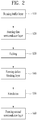
- FIG. 2 is a flowchart of a method for manufacturing a hetero-substrate. Hereinafter, the method for manufacturing the hetero-substrate will be described with reference to Figure 2 and other drawings.
- a buffer layer 20 is formed on a base substrate 10 (S10) and a first semiconductor layer 30 is formed on the buffer layer 20 (S20).
- a plurality of dislocations A may be formed on the buffer layer 20. Some of the dislocations may be removed due to direction conversion or the like. Accordingly, a dislocation density of the first semiconductor layer 30 may be lower than that of the buffer layer 20.
- a surface of the first semiconductor layer 30 is fetched (S30) to form a plurality of pits 31 having inclined surfaces.
- the formation of the pits 31 may be carried out by high-temperature dry etching.
- the first semiconductor layer 30 that includes a nitride semiconductor
- injection of source material may be stopped and high-temperature dry etching may be performed under a hydrogen (H2) atmosphere at an elevated temperature of 1,200°C at a position (e.g., height) in which the defect blocking layer 40 is to be formed.
- H2 hydrogen
- a start point of the high-temperature dry etching of the nitride semiconductor thin film may predominantly be at a dislocation position. Accordingly, as shown in Figure 4 , a surface, which is etched around dislocations, is obtained. For example, the pits 31 having inclined surfaces around dislocations may be formed. The pits 31 are referred to herein as dislocation etch pits.
- a defect blocking layer 40 that includes the plurality of metal droplets 41 is formed on a first semiconductor layer 30 including the pits 31 (S40).
- Formation of the metal droplets 41 may be carried out using at least one of gallium (Ga), indium (In) or aluminum (Al) after decreasing a temperature of a growth apparatus for forming the semiconductor to about 500°C or less.
- the formation of the metal droplet 41 is carried out using an organometallic source including at least one of Ga, In or Al.
- the formation may be carried out by supplying the organometallic source together with a carrier gas. At this time, supply of a nitrogen source (NH 3 ) injected upon formation of the nitride semiconductor may be stopped.
- a nitrogen source NH 3
- a first metal 43 such as Ga, In or Al is formed, and a second metal 42 such as gold (Au), silver (Ag), copper (Cu), platinum (Pt), nickel (Ni), chromium (Cr) or palladium (Pd) is then be formed on the first metal 43.
- a second metal 42 such as gold (Au), silver (Ag), copper (Cu), platinum (Pt), nickel (Ni), chromium (Cr) or palladium (Pd) is then be formed on the first metal 43.
- the formation of the second metal 42 is carried out using an organometallic source that includes at least one of Au, Ag, Cu, Pt, Ni, Cr or Pd, similar to formation of the first metal 43.
- the formation of the second metal 42 may be carried out by supplying the organometallic source together with a carrier gas.
- a temperature at which the second metal 42 is formed may be lower than that of the first metal particle 43.
- the metal droplets 41 thus formed may have a shape shown in Figure 6 or 7 .
- the first metal 43 is coated with the second metal 42 to constitute a particle (droplet) and the particle is disposed on an upper side of the first semiconductor layer 30 or the inclined surfaces of the pits 31.
- the first metal 43 may adhere to at least one side of the first semiconductor layer 30 or the pits 31, and the first metal 43 is coated with the second metal 42. In this case, only the exposed portion of the first metal 43 may be coated.
- a density of the metal droplets 41 may be 1 ⁇ 10 18 cm -2 or more, with respect to an area of the first semiconductor layer 30 or the defect blocking layer 40.
- first metal 43 may readily transform into a nitride semiconductor during a subsequent nitridation process, and may not maintain its metal shape.
- metal droplets of the first metal 43 are protected by covering the first metal 43 of the first type with the second metal 42 of the second type.
- An increase in dislocations upon subsequent nitridation and nitride semiconductor thin film formation may be prevented by forming a solid solution.
- the surfaces of metal droplets 41 on the first semiconductor layer 30 are subjected to nitridation by injecting a nitrogen source (NH 3 ) into a growth apparatus (S50).
- a nitrogen source NH 3
- a second semiconductor layer 50 that includes a nitride semiconductor is formed on the nitridated defect blocking layer 40 (S60).
- a temperature of the growth apparatus may be elevated to 500 to 600°C and a nitride semiconductor thin film protective layer may be grown at a temperature lower than a nitride semiconductor growth temperature to a thickness of about several tens to about several hundred nanometers.
- the surface may not completely be two-dimensionally flat, but may still function to prevent movement of the metal constituting the metal droplets 41 upward using a relatively low temperature and to offset dislocation at the dislocation point.
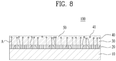
- a semiconductor thin film including a nitride semiconductor is grown at a high temperature to obtain a flat surface, as illustrated in Fig. 8 .
- the growth of the second semiconductor layer 50 may include primarily forming a protective layer at a relatively low temperature and secondarily forming a nitride semiconductor layer having a flat surface at a high temperature.
- the growth of the hetero-substrate 100 may be carried out by a method such as MOCVD or HVPE.
- the defect blocking layer 40 that includes the metal droplets 41 may be formed in-situ in the nitride semiconductor growth apparatus.
- the formation of the defect blocking layer 40 may be carried out in a nitride semiconductor (such as gallium nitride, GaN) thin film growth apparatus, a thin film hetero-substrate 100 may be grown in a single stage without outflow of samples.
- a nitride semiconductor such as gallium nitride, GaN
- formation of the hetero-substrate 100 may be effective in improving production efficiency of devices using a nitride semiconductor thin film and reducing cost thereof.
- Various semiconductor devices using a nitride semiconductor may be manufactured, based on the hetero-substrate 100.
- Such a semiconductor device may include a light emitting device such as a nitride light emitting diode or a laser diode, a transistor device such as an IGBT or HEMT, and the like.
- a light emitting device such as a nitride light emitting diode or a laser diode
- a transistor device such as an IGBT or HEMT, and the like.
- a semiconductor structure 200 that includes an n-type semiconductor layer 210, an active layer 220 and a p-type semiconductor layer 230 may be formed on the hetero-substrate 100.
- a transparent conductive layer 310 may be formed on the semiconductor structure 200 and a p-type electrode 300 may be formed on the transparent conductive layer 310.
- an n-type electrode 400 may be formed on the n-type semiconductor layer 210 to manufacture a lateral light emitting diode as shown in Figure 9 .
- manufacture of a vertical light emitting diode may be possible.
- the hetero-substrate 100 used as the growth substrate may be removed.
- the semiconductor structure 200 that includes the n-type semiconductor layer 210, the active layer 220 and the p-type semiconductor layer 230 may be grown on the hetero-substrate 100.
- a p-type electrode 320 may be formed on the p-type semiconductor layer 230 and a support layer 500 may be adhered to the p-type electrode 320 using a solder layer 510.
- the support layer 500 may include a metal or a semiconductor.
- the hetero-substrate 100 may be removed from the resulting structure supported by the support layer 500 to expose the n-type semiconductor layer 210.
- an n-type electrode 410 is formed on the exposed surface, a vertical light emitting diode structure as shown in Figure 10 may be obtained.
- a light extraction structure 211 may be formed on an upper surface of the n-type semiconductor layer 210.
- the pits 31 that includes the inclined surface described above may be exposed.
- the shape of the pit 31 may be transferred to the n-type semiconductor layer 210 by etching, and a light extraction structure 211 that includes the transferred shape may be obtained.
- the pits 31 may serve as a light extraction structure, thus advantageously improving light output of the light emitting device.
- the present disclosure is directed to a substrate having a hetero-structure, a method for manufacturing the same, and a nitride semiconductor light emitting device using the same.
Landscapes
- Led Devices (AREA)
- Crystals, And After-Treatments Of Crystals (AREA)
- Chemical & Material Sciences (AREA)
- Crystallography & Structural Chemistry (AREA)
Description
- The present invention relates to a method for manufacturing a nitride semiconductor, and more specifically, to a substrate having a hetero-structure (hereinafter, referred to simply as a "hetero-substrate").
- A light emitting device represented by a light emitting diode (LED) provides various colors through a p-n junction diode which converts electrical energy into light energy by controlling a compositional ratio of a compound semiconductor produced using a compound of Group III and V elements on the periodic table.
- Nitride semiconductors have attracted much attention in the field of development of optical devices and high-power electronic elements due to high thermal stability and wide band-gap energy thereof. In particular, blue light emitting devices, green light emitting devices, UV light emitting devices and the like using nitride semiconductors are commercialized and have entered widespread use.
- The light emitting device using such a nitride semiconductor may be implemented on a hetero-substrate made of materials such as sapphire or silicon carbide (SiC).
- As such, when nitride semiconductor thin films having a hetero-junction are grown using a sapphire substrate or other hetero-substrates or the like, differences in lattice mismatch and coefficient of thermal expansion caused by the hetero-junction may cause high crystal defects and high strain in thin films.
- Regarding the nitride semiconductor thin films grown on a sapphire substrate, development of low-temperature gallium nitride (GaN) and low-temperature aluminum nitride (AlN) buffers and the like have been investigated in order to reduce dislocation generated on the substrate, such that defect density is reduced to some extent. However, the nitride semiconductor thin films still have a high defect density of about 108 cm-2.
- In addition, when a hetero-junction is formed on a silicon (Si) substrate, dislocation density may still be high in spite of applying various thin film growth methods. In particular, in the process of cooling gallium nitride semiconductors grown at a high temperature to room temperature, there are problems associated with tensile strain applied to the thin film due to differences in coefficient of thermal expansion between the thin film and the Si substrate.
- Meanwhile, although growth of nitride semiconductor thin films using a GaN substrate may be the most superior growth method developed to date, production methods of GaN substrates have technical problems hindering commercialization, and entail cost several tens to several hundred times the cost of hetero-substrates, such as sapphire or Si, in terms of economic efficiency, thus restricting widespread use of GaN as a substrate.
- The above references are incorporated by reference herein where appropriate for appropriate teachings of additional or alternative details, features and/or technical background.
-
US 2004/067648 A1 relates to a crystal foundation having dislocations to obtain a crystal film of low dislocation density, a crystal substrate, and a semiconductor device. One side of a growth substrate is provided with a crystal layer with a buffer layer in between. The crystal layer has spaces in an end of each threading dislocation D1 elongating from below. The threading dislocation D1 is separated from the upper layer by the spaces so that each threading dislocation D1 is blocked from propagating to the upper layer. As a result, the upper layer above the spaces turns crystalline with a low dislocation density. -
US 2006/205197 A1 relates to a semiconductor device and method of manufacturing the same. The method includes coating a plurality of spherical balls on a substrate and selectively growing a compound semiconductor thin film on the substrate on which the spherical balls are coated. -
US 2009/008652 A1 relates to a free-standing substrate, a method for producing the same and a semiconductor light-emitting device. The free-standing substrate comprises a semiconductor layer and inorganic particles, wherein the inorganic particles are included in the semiconductor layer. The method for producing a free-standing substrate comprises the steps of: (a) placing inorganic particles on a substrate, (b) growing a semiconductor layer thereon, and (c) separating the semiconductor layer from the substrate, in that order. The semiconductor light-emitting device comprises the free-standing substrate, a conductive layer, a light-emitting device, and electrodes. - Accordingly, the present invention is directed to a method for manufacturing substrate having a hetero-structure.
- It is one object of the present invention to provide a hetero-substrate which minimizes crystal defects that may be generated during hetero-thin film growth and a method for manufacturing the same.
- The object is solved by the features of the independent claim.
- Additional advantages, objects, and features of the invention will be set forth in part in the description which follows and in part will become apparent to those having ordinary skill in the art upon examination of the following or may be learned from practice of the invention. The objectives and other advantages of the invention may be realized and attained by the structure particularly pointed out in the written description and claims hereof as well as the appended drawings.
- A hetero-substrate includes a base substrate, a buffer layer disposed on the base substrate, a first semiconductor layer disposed on the buffer layer, the first semiconductor layer including a nitride semiconductor, a defect blocking layer disposed on the first semiconductor layer, the defect blocking layer including a plurality of metal droplets, and a second semiconductor layer disposed on the defect blocking layer, the second semiconductor layer including a nitride semiconductor.
- In accordance with the present invention, a method for manufacturing a hetero-substrate includes forming a buffer layer on a base substrate, forming a first semiconductor layer that includes a nitride semiconductor on the buffer layer, etching a surface of the first semiconductor layer to form a plurality of dislocation etch pits, forming a defect blocking layer that includes a plurality of metal droplets on the etched surface of the first semiconductor layer, subjecting a surface of the first semiconductor layer provided with the defect blocking layer to nitridation, and forming a second semiconductor layer that includes a nitride semiconductor on the defect blocking layer.
- It is to be understood that both the foregoing general description and the following detailed description of the present invention are exemplary and explanatory and are intended to provide further explanation of the invention as claimed.
- The embodiments will be described in detail with reference to the following drawings in which like reference numerals refer to like elements wherein:
-
Figure 1 shows an example of a hetero-substrate; -
Figure 2 is a flowchart illustrating an example of a method for manufacturing a hetero-substrate; -
Figure 3 is a sectional view illustrating a state in which a buffer layer and a first semiconductor layer are formed; -
Figure 4 is a sectional view illustrating a state in which a surface of the first semiconductor layer is etched; -
Figure 5 is a sectional view illustrating a state in which a defect blocking layer is formed; -
Figure 6 is a schematic view illustrating an example in which metal droplets are formed; -
Figure 7 is a schematic view illustrating another example in which metal droplets are formed; -
Figure 8 is a sectional view illustrating a state in which a second semiconductor layer is formed; -
Figure 9 is a sectional view illustrating an example of a light emitting device manufactured using the hetero-substrate; and -
Figure 10 is a sectional view illustrating an example of a light emitting device manufactured using the hetero-substrate. - Reference will now be made in detail to the preferred embodiments of the present invention, examples of which are illustrated in the accompanying drawings. Wherever possible, the same reference numbers will be used throughout the drawings to refer to the same or like parts.
- However, the present invention allows various modifications and variations and specific embodiments thereof are exemplified through drawings and will be described in detail. The present invention should not be construed as limited to the embodiments set forth herein and includes modifications, variations, equivalents, and substitutions compliant with the scope of the present invention defined by the appended claims.
- It will be understood that when an element such as a layer, area, or substrate is referred to as being "on" another element, it can be directly on the element, or one or more intervening elements may also be present.
- In addition, it will be understood that although terms such as "first" and "second" may be used herein to describe elements, components, areas, layers and/or regions, the elements, components, areas, layers and/or regions should not be limited by these terms.
-
Figure 1 shows an example of a hetero-substrate 100 useful for the understanding of the inventive manufacturing method. A hetero-substrate or hetero-structure as used herein may refer to a semiconductor having multiple layers. The hetero-substrate 100 may include abase substrate 10. Thebase substrate 10 may be a sapphire or silicon (Si) substrate, but is not limited thereto. - A
buffer layer 20 is disposed on thebase substrate 10. Thebuffer layer 20 may include a nucleation layer that enables formation of a nitride semiconductor by hetero-junction on a substrate. The substrate may be a substrate other than a nitride semiconductor substrate, such as a sapphire or silicon (Si) substrate. Thebuffer layer 20 may also serve as the nucleation layer. - A
first semiconductor layer 30 that includes a nitride semiconductor is disposed on thebuffer layer 20. The nitride semiconductor may be a semiconductor containing nitride such as gallium nitride (GaN), aluminum nitride (AlN), aluminum gallium nitride (AlGaN), indium gallium nitride (InGaN), or another appropriate type of material. - A
defect blocking layer 40 that includes a plurality ofmetal droplets 41 is disposed on thefirst semiconductor layer 30. - The
metal droplets 41 are made of a mixture of two or more metal materials. Asecond metal 42 of a second type is disposed on afirst metal 43 of a first type (see, for example,Figure 6 ). Thefirst metal 43 is coated with thesecond metal 42. - The
first metal 43 includes at least one of Ga, In or Al, and thesecond metal 42 includes at least one of Au, Ag, Cu, Pt, Ni, Cr or Pd. - Meanwhile, a density of the
metal droplets 41 may be 1 × 1018 cm-2 or more, with respect to the overall area of thedefect blocking layer 40. - Such a
metal droplet 41 may function to block crystal defects, such as dislocation, of the semiconductor. - When a nitride semiconductor is formed on a
heterogeneous base substrate 10, threading dislocation A may occur to cause defects or irregularities in the semiconductor. The dislocation may extend from thebuffer layer 20 that includes the nucleation layer into thefirst semiconductor layer 30. - As illustrated in
Figure 1 , the threading dislocation A may be blocked by thedefect blocking layer 40 that includes themetal droplets 41 and a high-quality nitride semiconductor with a greatly reduced dislocation density may thus be formed on thedefect blocking layer 40. - In addition, the
defect blocking layer 40 is formed on theheterogeneous base substrate 10, thus functioning to reduce internal strain. - For example, internal strain may remain due to differences in crystal lattice constant between the materials such as sapphire or silicon and the nitride semiconductor. This internal strain may be reduced by the
defect blocking layer 40. - The
defect blocking layer 40 may include one or more types ofmetal droplets 41. - A
second semiconductor layer 50 is disposed on thedefect blocking layer 40. Thedefect blocking layer 40 may allow thesecond semiconductor layer 50 to be a high-quality nitride semiconductor having a reduced dislocation density and internal strain. - Because dislocation and defect density of the hetero-
substrate 100 having this structure are reduced by thedefect blocking layer 40 that includes the plurality ofmetal droplets 41, a low-dislocation, low-defect, high-quality nitride semiconductor thin film may be grown on the hetero-substrate 100. - In addition, tensile strain of the nitride semiconductor thin film grown on the hetero-
substrate 100 may be reduced and cracks, which may be generated upon growth of thin films having a high thickness, may thus be prevented. - Furthermore, substrate bending or the like may be prevented and uniformity of composition of thin films formed on the hetero-
substrate 100, wavelength of the light emitting device, and the like, may thus be improved. -
Figure 2 is a flowchart of a method for manufacturing a hetero-substrate. Hereinafter, the method for manufacturing the hetero-substrate will be described with reference toFigure 2 and other drawings. - First, as shown in
Figure 3 , abuffer layer 20 is formed on a base substrate 10 (S10) and afirst semiconductor layer 30 is formed on the buffer layer 20 (S20). - As illustrated, a plurality of dislocations A may be formed on the
buffer layer 20. Some of the dislocations may be removed due to direction conversion or the like. Accordingly, a dislocation density of thefirst semiconductor layer 30 may be lower than that of thebuffer layer 20. - Then, as shown in
Figure 4 , a surface of thefirst semiconductor layer 30 is fetched (S30) to form a plurality ofpits 31 having inclined surfaces. - The formation of the
pits 31 may be carried out by high-temperature dry etching. - During formation of the
first semiconductor layer 30 that includes a nitride semiconductor, injection of source material may be stopped and high-temperature dry etching may be performed under a hydrogen (H2) atmosphere at an elevated temperature of 1,200°C at a position (e.g., height) in which thedefect blocking layer 40 is to be formed. - A start point of the high-temperature dry etching of the nitride semiconductor thin film may predominantly be at a dislocation position. Accordingly, as shown in
Figure 4 , a surface, which is etched around dislocations, is obtained. For example, thepits 31 having inclined surfaces around dislocations may be formed. Thepits 31 are referred to herein as dislocation etch pits. - As shown in
Figure 5 , adefect blocking layer 40 that includes the plurality ofmetal droplets 41 is formed on afirst semiconductor layer 30 including the pits 31 (S40). - Formation of the
metal droplets 41 may be carried out using at least one of gallium (Ga), indium (In) or aluminum (Al) after decreasing a temperature of a growth apparatus for forming the semiconductor to about 500°C or less. - The formation of the
metal droplet 41 is carried out using an organometallic source including at least one of Ga, In or Al. For example, the formation may be carried out by supplying the organometallic source together with a carrier gas. At this time, supply of a nitrogen source (NH3) injected upon formation of the nitride semiconductor may be stopped. - Meanwhile, as shown in
FIGs. 6 and 7 , afirst metal 43 such as Ga, In or Al is formed, and asecond metal 42 such as gold (Au), silver (Ag), copper (Cu), platinum (Pt), nickel (Ni), chromium (Cr) or palladium (Pd) is then be formed on thefirst metal 43. - The formation of the
second metal 42 is carried out using an organometallic source that includes at least one of Au, Ag, Cu, Pt, Ni, Cr or Pd, similar to formation of thefirst metal 43. For example, the formation of thesecond metal 42 may be carried out by supplying the organometallic source together with a carrier gas. - In addition, a temperature at which the
second metal 42 is formed may be lower than that of thefirst metal particle 43. - The
metal droplets 41 thus formed may have a shape shown inFigure 6 or 7 . As shown inFigure 6 , thefirst metal 43 is coated with thesecond metal 42 to constitute a particle (droplet) and the particle is disposed on an upper side of thefirst semiconductor layer 30 or the inclined surfaces of thepits 31. - In addition, as shown in
Figure 7 , thefirst metal 43 may adhere to at least one side of thefirst semiconductor layer 30 or thepits 31, and thefirst metal 43 is coated with thesecond metal 42. In this case, only the exposed portion of thefirst metal 43 may be coated. - A density of the
metal droplets 41 may be 1×1018 cm-2 or more, with respect to an area of thefirst semiconductor layer 30 or thedefect blocking layer 40. - One of the reason for forming the
first metal 43 and thesecond metal 42 as described above is that thefirst metal 43 may readily transform into a nitride semiconductor during a subsequent nitridation process, and may not maintain its metal shape. - As such, when the
first metal 43 does not maintain its shape, offset effect of dislocations in a surface dislocation point of thefirst semiconductor layer 30 exposed by etching may be reduced. - Accordingly, metal droplets of the
first metal 43 are protected by covering thefirst metal 43 of the first type with thesecond metal 42 of the second type. An increase in dislocations upon subsequent nitridation and nitride semiconductor thin film formation may be prevented by forming a solid solution. - Next, the surfaces of
metal droplets 41 on thefirst semiconductor layer 30 are subjected to nitridation by injecting a nitrogen source (NH3) into a growth apparatus (S50). - Next, as shown in
Fig. 8 , asecond semiconductor layer 50 that includes a nitride semiconductor is formed on the nitridated defect blocking layer 40 (S60). - After growth of the
metal droplets 41, a temperature of the growth apparatus may be elevated to 500 to 600°C and a nitride semiconductor thin film protective layer may be grown at a temperature lower than a nitride semiconductor growth temperature to a thickness of about several tens to about several hundred nanometers. - In this process, the surface may not completely be two-dimensionally flat, but may still function to prevent movement of the metal constituting the
metal droplets 41 upward using a relatively low temperature and to offset dislocation at the dislocation point. - Next, a semiconductor thin film including a nitride semiconductor is grown at a high temperature to obtain a flat surface, as illustrated in
Fig. 8 . - For example, the growth of the
second semiconductor layer 50 may include primarily forming a protective layer at a relatively low temperature and secondarily forming a nitride semiconductor layer having a flat surface at a high temperature. - When the
second semiconductor layer 50 is formed as described above, a structure of the hetero-substrate 100 as shown inFigure 1 may be obtained. - The growth of the hetero-
substrate 100 may be carried out by a method such as MOCVD or HVPE. Thedefect blocking layer 40 that includes themetal droplets 41 may be formed in-situ in the nitride semiconductor growth apparatus. - For example, because the formation of the
defect blocking layer 40 may be carried out in a nitride semiconductor (such as gallium nitride, GaN) thin film growth apparatus, a thin film hetero-substrate 100 may be grown in a single stage without outflow of samples. - Accordingly, formation of the hetero-
substrate 100 may be effective in improving production efficiency of devices using a nitride semiconductor thin film and reducing cost thereof. - Various semiconductor devices using a nitride semiconductor may be manufactured, based on the hetero-
substrate 100. - Such a semiconductor device may include a light emitting device such as a nitride light emitting diode or a laser diode, a transistor device such as an IGBT or HEMT, and the like.
- Hereinafter, a process of manufacturing a light emitting device such as a light emitting diode on the hetero-
substrate 100 will be briefly described. - First, as shown in
Figure 9 , asemiconductor structure 200 that includes an n-type semiconductor layer 210, anactive layer 220 and a p-type semiconductor layer 230 may be formed on the hetero-substrate 100. - Next, a transparent
conductive layer 310 may be formed on thesemiconductor structure 200 and a p-type electrode 300 may be formed on the transparentconductive layer 310. - After etching to expose the n-
type semiconductor layer 210, an n-type electrode 400 may be formed on the n-type semiconductor layer 210 to manufacture a lateral light emitting diode as shown inFigure 9 . - Meanwhile, as shown in
Figure 10 , manufacture of a vertical light emitting diode may be possible. In the vertical light emitting diode, the hetero-substrate 100 used as the growth substrate may be removed. - Reference to
Figure 1 . in the vertical light emitting diode, thesemiconductor structure 200 that includes the n-type semiconductor layer 210, theactive layer 220 and the p-type semiconductor layer 230 may be grown on the hetero-substrate 100. - In addition, a p-
type electrode 320 may be formed on the p-type semiconductor layer 230 and asupport layer 500 may be adhered to the p-type electrode 320 using asolder layer 510. Thesupport layer 500 may include a metal or a semiconductor. - Next, the hetero-
substrate 100 may be removed from the resulting structure supported by thesupport layer 500 to expose the n-type semiconductor layer 210. When an n-type electrode 410 is formed on the exposed surface, a vertical light emitting diode structure as shown inFigure 10 may be obtained. - A
light extraction structure 211 may be formed on an upper surface of the n-type semiconductor layer 210. - During removal of the hetero-
substrate 100, thepits 31 that includes the inclined surface described above may be exposed. When etching is performed upon thepit 31, the shape of thepit 31 may be transferred to the n-type semiconductor layer 210 by etching, and alight extraction structure 211 that includes the transferred shape may be obtained. - Accordingly, the
pits 31 may serve as a light extraction structure, thus advantageously improving light output of the light emitting device. - The present disclosure is directed to a substrate having a hetero-structure, a method for manufacturing the same, and a nitride semiconductor light emitting device using the same.
- It is one object of the present disclosure to provide a hetero-substrate which minimizes crystal defects that may be generated during hetero-thin film growth, a method for manufacturing the same, and a nitride semiconductor light emitting device using the same.
Claims (4)
- A method for manufacturing a hetero-substrate comprising:forming (S10) a buffer layer (20) on a base substrate (10);forming (S20) a first semiconductor layer (30) that includes a nitride semiconductor on the buffer layer (20);etching (S30) a surface of the first semiconductor layer (30) to form a plurality of dislocation etch pits;forming (S40) a defect blocking layer (40) that includes a plurality of metal droplets (41) on the etched surface of the first semiconductor layer (30),subjecting (S50) a surface of the first semiconductor layer (30) provided with the defect blocking layer (40) to nitridation; andforming (S60) a second semiconductor layer (50) that includes a nitride semiconductor on the defect blocking layer (40),wherein the metal droplets (41) comprise a first metal (43) and a second metal (42), wherein the formation of the defect blocking layer (40) comprises:forming the first metal (43) of a first type on a surface of the first semiconductor layer (30); andforming the second metal (42) of a second type on the first metal (43), the first and second metal types being different types of metals,wherein the first metal (43) is coated with the second metal (42),wherein the first metal (43) of the first type comprises at least one of Ga, In or Al, andwherein the second metal (42) of the second type comprises at least one of Au, Ag, Cu, Pt, Ni, Cr or Pd.
- The method according to claim 1, wherein a formation temperature of the second metal (42) is lower than that of the first metal (43).
- The method according to one of the claims 1 or 2, wherein the formation (S40) of the defect blocking layer (40) on the first semiconductor layer is carried out in-situ using an organometallic source.
- The method according to one of the claims 1 to 3, wherein the metal droplets (41) are disposed on a plurality of pits (31) having an inclined surface formed by etching (S30) the surface of the first semiconductor layer (30).
Applications Claiming Priority (1)
| Application Number | Priority Date | Filing Date | Title |
|---|---|---|---|
| KR1020130051781A KR102015914B1 (en) | 2013-05-08 | 2013-05-08 | substrate having hetero-structure, nitride semiconductor light emitting device using the same and method for manufacturing the same |
Publications (2)
| Publication Number | Publication Date |
|---|---|
| EP2802002A1 EP2802002A1 (en) | 2014-11-12 |
| EP2802002B1 true EP2802002B1 (en) | 2021-02-03 |
Family
ID=49680903
Family Applications (1)
| Application Number | Title | Priority Date | Filing Date |
|---|---|---|---|
| EP13195283.0A Active EP2802002B1 (en) | 2013-05-08 | 2013-12-02 | Method for the manufacturing of a substrate having a hetero-structure |
Country Status (3)
| Country | Link |
|---|---|
| US (1) | US9257602B2 (en) |
| EP (1) | EP2802002B1 (en) |
| KR (1) | KR102015914B1 (en) |
Families Citing this family (6)
| Publication number | Priority date | Publication date | Assignee | Title |
|---|---|---|---|---|
| CN109417020A (en) * | 2016-04-12 | 2019-03-01 | 璐米斯塔尔有限公司 | Manufacturing method of nitride semiconductor substrate including semi-insulating nitride semiconductor layer and nitride semiconductor substrate manufactured by the method |
| KR102604087B1 (en) | 2016-06-24 | 2023-11-21 | 삼성디스플레이 주식회사 | Window and display apparatus having the same |
| US10665752B2 (en) * | 2017-12-15 | 2020-05-26 | Saphlux, Inc. | Air void structures for semiconductor fabrication |
| US11767609B2 (en) | 2018-02-09 | 2023-09-26 | Sixpoint Materials, Inc. | Low-dislocation bulk GaN crystal and method of fabricating same |
| KR20210109997A (en) | 2020-02-28 | 2021-09-07 | 한국산업기술대학교산학협력단 | The Manufacturing Method of the Nitride Semiconductor Device |
| CN116525730B (en) * | 2023-07-05 | 2023-09-08 | 江西兆驰半导体有限公司 | A method for preparing a light-emitting diode epitaxial wafer and an epitaxial wafer |
Citations (1)
| Publication number | Priority date | Publication date | Assignee | Title |
|---|---|---|---|---|
| US20090008652A1 (en) * | 2005-03-22 | 2009-01-08 | Sumitomo Chemical Company, Ltd. | Free-Standing Substrate, Method for Producing the Same and Semiconductor Light-Emitting Device |
Family Cites Families (8)
| Publication number | Priority date | Publication date | Assignee | Title |
|---|---|---|---|---|
| JP3988018B2 (en) * | 2001-01-18 | 2007-10-10 | ソニー株式会社 | Crystal film, crystal substrate and semiconductor device |
| KR100712753B1 (en) * | 2005-03-09 | 2007-04-30 | 주식회사 실트론 | Compound Semiconductor Device and Manufacturing Method Thereof |
| JP2007001855A (en) * | 2005-05-27 | 2007-01-11 | Sumitomo Chemical Co Ltd | 3-5 nitride semiconductor multilayer substrate, 3-5 nitride semiconductor free-standing substrate manufacturing method, and semiconductor device |
| WO2009070625A1 (en) * | 2007-11-27 | 2009-06-04 | Nanocrystal, Llc | Ultra-low dislocation density group iii - nitride semiconductor substrates grown via nano-or micro-particle film |
| JP5191866B2 (en) * | 2008-11-12 | 2013-05-08 | スタンレー電気株式会社 | Semiconductor light emitting device manufacturing method and semiconductor light emitting device |
| KR101038923B1 (en) * | 2010-02-02 | 2011-06-03 | 전북대학교산학협력단 | Light emitting diode having improved luminous efficiency and manufacturing method thereof |
| US8723159B2 (en) * | 2011-02-15 | 2014-05-13 | Invenlux Corporation | Defect-controlling structure for epitaxial growth, light emitting device containing defect-controlling structure, and method of forming the same |
| KR101982626B1 (en) * | 2012-10-17 | 2019-05-27 | 엘지이노텍 주식회사 | Light emitting device and lighting device having the same |
-
2013
- 2013-05-08 KR KR1020130051781A patent/KR102015914B1/en active Active
- 2013-12-02 EP EP13195283.0A patent/EP2802002B1/en active Active
- 2013-12-06 US US14/098,878 patent/US9257602B2/en active Active
Patent Citations (1)
| Publication number | Priority date | Publication date | Assignee | Title |
|---|---|---|---|---|
| US20090008652A1 (en) * | 2005-03-22 | 2009-01-08 | Sumitomo Chemical Company, Ltd. | Free-Standing Substrate, Method for Producing the Same and Semiconductor Light-Emitting Device |
Also Published As
| Publication number | Publication date |
|---|---|
| US20140332833A1 (en) | 2014-11-13 |
| US9257602B2 (en) | 2016-02-09 |
| KR20140132524A (en) | 2014-11-18 |
| EP2802002A1 (en) | 2014-11-12 |
| KR102015914B1 (en) | 2019-08-29 |
Similar Documents
| Publication | Publication Date | Title |
|---|---|---|
| US8878189B2 (en) | Group III nitride semiconductor growth substrate, group III nitride semiconductor epitaxial substrate, group III nitride semiconductor element and group III nitride semiconductor free-standing substrate, and method of producing the same | |
| KR101535764B1 (en) | Gallium nitride wafer substrate for solid state lighting devices, and associated systems and methods | |
| US8436362B2 (en) | Solid state lighting devices with selected thermal expansion and/or surface characteristics, and associated methods | |
| US20110124139A1 (en) | Method for manufacturing free-standing substrate and free-standing light-emitting device | |
| EP2615628B1 (en) | Method of growing nitride semiconductor layer | |
| EP2802002B1 (en) | Method for the manufacturing of a substrate having a hetero-structure | |
| US10014436B2 (en) | Method for manufacturing a light emitting element | |
| TWI407491B (en) | Method of separating semiconductor and its substrate | |
| JP2005527988A (en) | Gallium nitride base device and manufacturing method | |
| KR20120057169A (en) | Opto-electric device, forming method of opto-electric device | |
| US20060124956A1 (en) | Quasi group III-nitride substrates and methods of mass production of the same | |
| US7859086B2 (en) | Nitride semiconductor single crystal substrate, and methods of fabricating the same and a vertical nitride semiconductor light emitting diode using the same | |
| CN103996610B (en) | AlN thin film growing on metal aluminum substrate and preparing method and application thereof | |
| US20140151714A1 (en) | Gallium nitride substrate and method for fabricating the same | |
| CN103872200B (en) | Form the method for semiconductor layer, light emitting semiconductor device and manufacture method thereof | |
| CN106328774A (en) | Epitaxial growth method and application of GaN film | |
| KR100834698B1 (en) | Gallium nitride thin film forming method and gallium nitride thin film substrate produced by the method | |
| KR100858362B1 (en) | Manufacturing Method of Vertical Light Emitting Diode Device | |
| KR102094990B1 (en) | Method for growing nitride semiconductor | |
| CN105633232A (en) | GaN LED epitaxial structure with GaN buffering layer substrate, and preparation method for GaN LED epitaxial structure | |
| CN103972336A (en) | Method for prolonging working life of GaN-based LED device in temperature circulation manner | |
| JP2010278470A (en) | Substrate for growing group-iii nitride semiconductor, epitaxial substrate for group-iii nitride semiconductor, group-iii nitride semiconductor element, stand-alone substrate for group-iii nitride semiconductor, and methods for manufacturing the same | |
| CN102110751A (en) | Self-supporting GaN-based luminescent device and manufacturing method thereof | |
| KR101901932B1 (en) | Substrate having heterostructure, nitride-based semiconductor light emitting device and method for manufacturing the same |
Legal Events
| Date | Code | Title | Description |
|---|---|---|---|
| PUAI | Public reference made under article 153(3) epc to a published international application that has entered the european phase |
Free format text: ORIGINAL CODE: 0009012 |
|
| 17P | Request for examination filed |
Effective date: 20140331 |
|
| AK | Designated contracting states |
Kind code of ref document: A1 Designated state(s): AL AT BE BG CH CY CZ DE DK EE ES FI FR GB GR HR HU IE IS IT LI LT LU LV MC MK MT NL NO PL PT RO RS SE SI SK SM TR |
|
| AX | Request for extension of the european patent |
Extension state: BA ME |
|
| 17Q | First examination report despatched |
Effective date: 20150713 |
|
| STAA | Information on the status of an ep patent application or granted ep patent |
Free format text: STATUS: EXAMINATION IS IN PROGRESS |
|
| RIC1 | Information provided on ipc code assigned before grant |
Ipc: H01L 21/02 20060101AFI20200519BHEP Ipc: H01L 33/00 20100101ALN20200519BHEP |
|
| GRAP | Despatch of communication of intention to grant a patent |
Free format text: ORIGINAL CODE: EPIDOSNIGR1 |
|
| STAA | Information on the status of an ep patent application or granted ep patent |
Free format text: STATUS: GRANT OF PATENT IS INTENDED |
|
| RIC1 | Information provided on ipc code assigned before grant |
Ipc: H01L 21/02 20060101AFI20200604BHEP Ipc: H01L 33/00 20100101ALN20200604BHEP |
|
| INTG | Intention to grant announced |
Effective date: 20200630 |
|
| RAP1 | Party data changed (applicant data changed or rights of an application transferred) |
Owner name: LG ELECTRONICS INC. |
|
| GRAS | Grant fee paid |
Free format text: ORIGINAL CODE: EPIDOSNIGR3 |
|
| GRAA | (expected) grant |
Free format text: ORIGINAL CODE: 0009210 |
|
| STAA | Information on the status of an ep patent application or granted ep patent |
Free format text: STATUS: THE PATENT HAS BEEN GRANTED |
|
| AK | Designated contracting states |
Kind code of ref document: B1 Designated state(s): AL AT BE BG CH CY CZ DE DK EE ES FI FR GB GR HR HU IE IS IT LI LT LU LV MC MK MT NL NO PL PT RO RS SE SI SK SM TR |
|
| REG | Reference to a national code |
Ref country code: GB Ref legal event code: FG4D |
|
| REG | Reference to a national code |
Ref country code: AT Ref legal event code: REF Ref document number: 1359873 Country of ref document: AT Kind code of ref document: T Effective date: 20210215 Ref country code: CH Ref legal event code: EP |
|
| REG | Reference to a national code |
Ref country code: DE Ref legal event code: R096 Ref document number: 602013075566 Country of ref document: DE |
|
| REG | Reference to a national code |
Ref country code: IE Ref legal event code: FG4D |
|
| REG | Reference to a national code |
Ref country code: NL Ref legal event code: MP Effective date: 20210203 |
|
| REG | Reference to a national code |
Ref country code: LT Ref legal event code: MG9D |
|
| REG | Reference to a national code |
Ref country code: AT Ref legal event code: MK05 Ref document number: 1359873 Country of ref document: AT Kind code of ref document: T Effective date: 20210203 |
|
| PG25 | Lapsed in a contracting state [announced via postgrant information from national office to epo] |
Ref country code: HR Free format text: LAPSE BECAUSE OF FAILURE TO SUBMIT A TRANSLATION OF THE DESCRIPTION OR TO PAY THE FEE WITHIN THE PRESCRIBED TIME-LIMIT Effective date: 20210203 Ref country code: GR Free format text: LAPSE BECAUSE OF FAILURE TO SUBMIT A TRANSLATION OF THE DESCRIPTION OR TO PAY THE FEE WITHIN THE PRESCRIBED TIME-LIMIT Effective date: 20210504 Ref country code: FI Free format text: LAPSE BECAUSE OF FAILURE TO SUBMIT A TRANSLATION OF THE DESCRIPTION OR TO PAY THE FEE WITHIN THE PRESCRIBED TIME-LIMIT Effective date: 20210203 Ref country code: LT Free format text: LAPSE BECAUSE OF FAILURE TO SUBMIT A TRANSLATION OF THE DESCRIPTION OR TO PAY THE FEE WITHIN THE PRESCRIBED TIME-LIMIT Effective date: 20210203 Ref country code: PT Free format text: LAPSE BECAUSE OF FAILURE TO SUBMIT A TRANSLATION OF THE DESCRIPTION OR TO PAY THE FEE WITHIN THE PRESCRIBED TIME-LIMIT Effective date: 20210604 Ref country code: BG Free format text: LAPSE BECAUSE OF FAILURE TO SUBMIT A TRANSLATION OF THE DESCRIPTION OR TO PAY THE FEE WITHIN THE PRESCRIBED TIME-LIMIT Effective date: 20210503 Ref country code: NO Free format text: LAPSE BECAUSE OF FAILURE TO SUBMIT A TRANSLATION OF THE DESCRIPTION OR TO PAY THE FEE WITHIN THE PRESCRIBED TIME-LIMIT Effective date: 20210503 |
|
| PG25 | Lapsed in a contracting state [announced via postgrant information from national office to epo] |
Ref country code: LV Free format text: LAPSE BECAUSE OF FAILURE TO SUBMIT A TRANSLATION OF THE DESCRIPTION OR TO PAY THE FEE WITHIN THE PRESCRIBED TIME-LIMIT Effective date: 20210203 Ref country code: RS Free format text: LAPSE BECAUSE OF FAILURE TO SUBMIT A TRANSLATION OF THE DESCRIPTION OR TO PAY THE FEE WITHIN THE PRESCRIBED TIME-LIMIT Effective date: 20210203 Ref country code: NL Free format text: LAPSE BECAUSE OF FAILURE TO SUBMIT A TRANSLATION OF THE DESCRIPTION OR TO PAY THE FEE WITHIN THE PRESCRIBED TIME-LIMIT Effective date: 20210203 Ref country code: PL Free format text: LAPSE BECAUSE OF FAILURE TO SUBMIT A TRANSLATION OF THE DESCRIPTION OR TO PAY THE FEE WITHIN THE PRESCRIBED TIME-LIMIT Effective date: 20210203 Ref country code: AT Free format text: LAPSE BECAUSE OF FAILURE TO SUBMIT A TRANSLATION OF THE DESCRIPTION OR TO PAY THE FEE WITHIN THE PRESCRIBED TIME-LIMIT Effective date: 20210203 Ref country code: SE Free format text: LAPSE BECAUSE OF FAILURE TO SUBMIT A TRANSLATION OF THE DESCRIPTION OR TO PAY THE FEE WITHIN THE PRESCRIBED TIME-LIMIT Effective date: 20210203 |
|
| PG25 | Lapsed in a contracting state [announced via postgrant information from national office to epo] |
Ref country code: IS Free format text: LAPSE BECAUSE OF FAILURE TO SUBMIT A TRANSLATION OF THE DESCRIPTION OR TO PAY THE FEE WITHIN THE PRESCRIBED TIME-LIMIT Effective date: 20210603 |
|
| PG25 | Lapsed in a contracting state [announced via postgrant information from national office to epo] |
Ref country code: CZ Free format text: LAPSE BECAUSE OF FAILURE TO SUBMIT A TRANSLATION OF THE DESCRIPTION OR TO PAY THE FEE WITHIN THE PRESCRIBED TIME-LIMIT Effective date: 20210203 Ref country code: EE Free format text: LAPSE BECAUSE OF FAILURE TO SUBMIT A TRANSLATION OF THE DESCRIPTION OR TO PAY THE FEE WITHIN THE PRESCRIBED TIME-LIMIT Effective date: 20210203 Ref country code: SM Free format text: LAPSE BECAUSE OF FAILURE TO SUBMIT A TRANSLATION OF THE DESCRIPTION OR TO PAY THE FEE WITHIN THE PRESCRIBED TIME-LIMIT Effective date: 20210203 |
|
| REG | Reference to a national code |
Ref country code: DE Ref legal event code: R097 Ref document number: 602013075566 Country of ref document: DE |
|
| PG25 | Lapsed in a contracting state [announced via postgrant information from national office to epo] |
Ref country code: RO Free format text: LAPSE BECAUSE OF FAILURE TO SUBMIT A TRANSLATION OF THE DESCRIPTION OR TO PAY THE FEE WITHIN THE PRESCRIBED TIME-LIMIT Effective date: 20210203 Ref country code: SK Free format text: LAPSE BECAUSE OF FAILURE TO SUBMIT A TRANSLATION OF THE DESCRIPTION OR TO PAY THE FEE WITHIN THE PRESCRIBED TIME-LIMIT Effective date: 20210203 Ref country code: ES Free format text: LAPSE BECAUSE OF FAILURE TO SUBMIT A TRANSLATION OF THE DESCRIPTION OR TO PAY THE FEE WITHIN THE PRESCRIBED TIME-LIMIT Effective date: 20210203 Ref country code: DK Free format text: LAPSE BECAUSE OF FAILURE TO SUBMIT A TRANSLATION OF THE DESCRIPTION OR TO PAY THE FEE WITHIN THE PRESCRIBED TIME-LIMIT Effective date: 20210203 |
|
| PLBE | No opposition filed within time limit |
Free format text: ORIGINAL CODE: 0009261 |
|
| STAA | Information on the status of an ep patent application or granted ep patent |
Free format text: STATUS: NO OPPOSITION FILED WITHIN TIME LIMIT |
|
| 26N | No opposition filed |
Effective date: 20211104 |
|
| PG25 | Lapsed in a contracting state [announced via postgrant information from national office to epo] |
Ref country code: AL Free format text: LAPSE BECAUSE OF FAILURE TO SUBMIT A TRANSLATION OF THE DESCRIPTION OR TO PAY THE FEE WITHIN THE PRESCRIBED TIME-LIMIT Effective date: 20210203 |
|
| PG25 | Lapsed in a contracting state [announced via postgrant information from national office to epo] |
Ref country code: SI Free format text: LAPSE BECAUSE OF FAILURE TO SUBMIT A TRANSLATION OF THE DESCRIPTION OR TO PAY THE FEE WITHIN THE PRESCRIBED TIME-LIMIT Effective date: 20210203 |
|
| PG25 | Lapsed in a contracting state [announced via postgrant information from national office to epo] |
Ref country code: IT Free format text: LAPSE BECAUSE OF FAILURE TO SUBMIT A TRANSLATION OF THE DESCRIPTION OR TO PAY THE FEE WITHIN THE PRESCRIBED TIME-LIMIT Effective date: 20210203 |
|
| PG25 | Lapsed in a contracting state [announced via postgrant information from national office to epo] |
Ref country code: IS Free format text: LAPSE BECAUSE OF FAILURE TO SUBMIT A TRANSLATION OF THE DESCRIPTION OR TO PAY THE FEE WITHIN THE PRESCRIBED TIME-LIMIT Effective date: 20210603 |
|
| PG25 | Lapsed in a contracting state [announced via postgrant information from national office to epo] |
Ref country code: MC Free format text: LAPSE BECAUSE OF FAILURE TO SUBMIT A TRANSLATION OF THE DESCRIPTION OR TO PAY THE FEE WITHIN THE PRESCRIBED TIME-LIMIT Effective date: 20210203 |
|
| REG | Reference to a national code |
Ref country code: CH Ref legal event code: PL |
|
| GBPC | Gb: european patent ceased through non-payment of renewal fee |
Effective date: 20211202 |
|
| REG | Reference to a national code |
Ref country code: BE Ref legal event code: MM Effective date: 20211231 |
|
| PG25 | Lapsed in a contracting state [announced via postgrant information from national office to epo] |
Ref country code: LU Free format text: LAPSE BECAUSE OF NON-PAYMENT OF DUE FEES Effective date: 20211202 Ref country code: IE Free format text: LAPSE BECAUSE OF NON-PAYMENT OF DUE FEES Effective date: 20211202 Ref country code: GB Free format text: LAPSE BECAUSE OF NON-PAYMENT OF DUE FEES Effective date: 20211202 |
|
| PG25 | Lapsed in a contracting state [announced via postgrant information from national office to epo] |
Ref country code: FR Free format text: LAPSE BECAUSE OF NON-PAYMENT OF DUE FEES Effective date: 20211231 Ref country code: BE Free format text: LAPSE BECAUSE OF NON-PAYMENT OF DUE FEES Effective date: 20211231 |
|
| PG25 | Lapsed in a contracting state [announced via postgrant information from national office to epo] |
Ref country code: LI Free format text: LAPSE BECAUSE OF NON-PAYMENT OF DUE FEES Effective date: 20211231 Ref country code: CH Free format text: LAPSE BECAUSE OF NON-PAYMENT OF DUE FEES Effective date: 20211231 |
|
| PG25 | Lapsed in a contracting state [announced via postgrant information from national office to epo] |
Ref country code: HU Free format text: LAPSE BECAUSE OF FAILURE TO SUBMIT A TRANSLATION OF THE DESCRIPTION OR TO PAY THE FEE WITHIN THE PRESCRIBED TIME-LIMIT; INVALID AB INITIO Effective date: 20131202 |
|
| PG25 | Lapsed in a contracting state [announced via postgrant information from national office to epo] |
Ref country code: CY Free format text: LAPSE BECAUSE OF FAILURE TO SUBMIT A TRANSLATION OF THE DESCRIPTION OR TO PAY THE FEE WITHIN THE PRESCRIBED TIME-LIMIT Effective date: 20210203 |
|
| PG25 | Lapsed in a contracting state [announced via postgrant information from national office to epo] |
Ref country code: MK Free format text: LAPSE BECAUSE OF FAILURE TO SUBMIT A TRANSLATION OF THE DESCRIPTION OR TO PAY THE FEE WITHIN THE PRESCRIBED TIME-LIMIT Effective date: 20210203 |
|
| PG25 | Lapsed in a contracting state [announced via postgrant information from national office to epo] |
Ref country code: MT Free format text: LAPSE BECAUSE OF FAILURE TO SUBMIT A TRANSLATION OF THE DESCRIPTION OR TO PAY THE FEE WITHIN THE PRESCRIBED TIME-LIMIT Effective date: 20210203 |
|
| PGFP | Annual fee paid to national office [announced via postgrant information from national office to epo] |
Ref country code: DE Payment date: 20241107 Year of fee payment: 12 |
|
| REG | Reference to a national code |
Ref country code: DE Ref legal event code: R079 Ref document number: 602013075566 Country of ref document: DE Free format text: PREVIOUS MAIN CLASS: H01L0021020000 Ipc: H10P0095000000 |
|
| PG25 | Lapsed in a contracting state [announced via postgrant information from national office to epo] |
Ref country code: TR Free format text: LAPSE BECAUSE OF FAILURE TO SUBMIT A TRANSLATION OF THE DESCRIPTION OR TO PAY THE FEE WITHIN THE PRESCRIBED TIME-LIMIT Effective date: 20210203 |