EP2801852A1 - Light-receiving package for flat-plate mounting, and optical module - Google Patents
Light-receiving package for flat-plate mounting, and optical module Download PDFInfo
- Publication number
- EP2801852A1 EP2801852A1 EP12864605.6A EP12864605A EP2801852A1 EP 2801852 A1 EP2801852 A1 EP 2801852A1 EP 12864605 A EP12864605 A EP 12864605A EP 2801852 A1 EP2801852 A1 EP 2801852A1
- Authority
- EP
- European Patent Office
- Prior art keywords
- light
- flat
- holder
- monitor
- retaining
- Prior art date
- Legal status (The legal status is an assumption and is not a legal conclusion. Google has not performed a legal analysis and makes no representation as to the accuracy of the status listed.)
- Withdrawn
Links
Images



Classifications
-
- G—PHYSICS
- G02—OPTICS
- G02B—OPTICAL ELEMENTS, SYSTEMS OR APPARATUS
- G02B6/00—Light guides; Structural details of arrangements comprising light guides and other optical elements, e.g. couplings
- G02B6/24—Coupling light guides
- G02B6/42—Coupling light guides with opto-electronic elements
- G02B6/4295—Coupling light guides with opto-electronic elements coupling with semiconductor devices activated by light through the light guide, e.g. thyristors, phototransistors
-
- G—PHYSICS
- G02—OPTICS
- G02B—OPTICAL ELEMENTS, SYSTEMS OR APPARATUS
- G02B6/00—Light guides; Structural details of arrangements comprising light guides and other optical elements, e.g. couplings
- G02B6/24—Coupling light guides
- G02B6/42—Coupling light guides with opto-electronic elements
- G02B6/4201—Packages, e.g. shape, construction, internal or external details
- G02B6/4286—Optical modules with optical power monitoring
-
- G—PHYSICS
- G02—OPTICS
- G02B—OPTICAL ELEMENTS, SYSTEMS OR APPARATUS
- G02B6/00—Light guides; Structural details of arrangements comprising light guides and other optical elements, e.g. couplings
- G02B6/10—Light guides; Structural details of arrangements comprising light guides and other optical elements, e.g. couplings of the optical waveguide type
- G02B6/12—Light guides; Structural details of arrangements comprising light guides and other optical elements, e.g. couplings of the optical waveguide type of the integrated circuit kind
-
- G—PHYSICS
- G02—OPTICS
- G02B—OPTICAL ELEMENTS, SYSTEMS OR APPARATUS
- G02B6/00—Light guides; Structural details of arrangements comprising light guides and other optical elements, e.g. couplings
- G02B6/10—Light guides; Structural details of arrangements comprising light guides and other optical elements, e.g. couplings of the optical waveguide type
- G02B6/12—Light guides; Structural details of arrangements comprising light guides and other optical elements, e.g. couplings of the optical waveguide type of the integrated circuit kind
- G02B6/13—Integrated optical circuits characterised by the manufacturing method
-
- G—PHYSICS
- G02—OPTICS
- G02B—OPTICAL ELEMENTS, SYSTEMS OR APPARATUS
- G02B6/00—Light guides; Structural details of arrangements comprising light guides and other optical elements, e.g. couplings
- G02B6/24—Coupling light guides
- G02B6/42—Coupling light guides with opto-electronic elements
- G02B6/4201—Packages, e.g. shape, construction, internal or external details
- G02B6/4202—Packages, e.g. shape, construction, internal or external details for coupling an active element with fibres without intermediate optical elements, e.g. fibres with plane ends, fibres with shaped ends, bundles
- G02B6/4203—Optical features
-
- G—PHYSICS
- G02—OPTICS
- G02B—OPTICAL ELEMENTS, SYSTEMS OR APPARATUS
- G02B6/00—Light guides; Structural details of arrangements comprising light guides and other optical elements, e.g. couplings
- G02B6/24—Coupling light guides
- G02B6/42—Coupling light guides with opto-electronic elements
- G02B6/4201—Packages, e.g. shape, construction, internal or external details
- G02B6/4256—Details of housings
- G02B6/4262—Details of housings characterised by the shape of the housing
- G02B6/4265—Details of housings characterised by the shape of the housing of the Butterfly or dual inline package [DIP] type
-
- H—ELECTRICITY
- H10—SEMICONDUCTOR DEVICES; ELECTRIC SOLID-STATE DEVICES NOT OTHERWISE PROVIDED FOR
- H10F—INORGANIC SEMICONDUCTOR DEVICES SENSITIVE TO INFRARED RADIATION, LIGHT, ELECTROMAGNETIC RADIATION OF SHORTER WAVELENGTH OR CORPUSCULAR RADIATION
- H10F77/00—Constructional details of devices covered by this subclass
- H10F77/50—Encapsulations or containers
-
- G—PHYSICS
- G02—OPTICS
- G02B—OPTICAL ELEMENTS, SYSTEMS OR APPARATUS
- G02B6/00—Light guides; Structural details of arrangements comprising light guides and other optical elements, e.g. couplings
- G02B6/10—Light guides; Structural details of arrangements comprising light guides and other optical elements, e.g. couplings of the optical waveguide type
- G02B6/12—Light guides; Structural details of arrangements comprising light guides and other optical elements, e.g. couplings of the optical waveguide type of the integrated circuit kind
- G02B2006/12133—Functions
- G02B2006/12138—Sensor
Definitions
- the present invention relates to a light-receiving package for flat-plate mounting, which is mounted with a monitor PD (PhotoDiode), and an optical module.
- monitor PD PhotoDiode
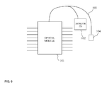
- a conventional monitor PD 102 has a coaxial structure with a fiber, and, as shown in FIG. 6 , an optical signal is tapped to an optical fiber 103 of an optical module 101 to connect the monitor PD 102 by fusion bonding and, thus, to monitor an output of the optical signal (for example, see
- Patent Literature 1 1).
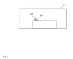
- FIG. 7 shows a conventional example in which the monitor PD 102 is integrated in the optical module 101 (for example, see Patent Literature 2).
- the monitor PD 102 is in a form in which a PD bare chip is mounted on a carrier such as ceramic.
- Patent Literature 2 since the PD bare chip is exposed inside the optical module, not only a main optical signal but also a stray light component generated in the optical module are received, and thus it is difficult to stably monitor the optical signal. Further, since the monitor PD is implemented without adjustment, there is a problem that reception sensitivity varies depending on a lot and mounting accuracy.
- an object of the present invention is to provide a light-receiving package for flat-plate mounting and an optical module which can make reception sensitivity constant without increasing the size of a module.
- a light-receiving package for flat-plate mounting of the present invention is provided with a first subassembly which has a photo diode and a retaining holder and in which the photo diode is fixed to a front surface of the retaining holder, a back surface of the retaining holder is a flat surface capable of moving parallel on a plane parallel to a light-receiving surface of the photo diode and a second subassembly which has the rectangular U-shaped concave holder for retaining the retaining holder and a flat-plate base disposed on a substrate and in which a surface of the flat-plate base that is mounted on the substrate is a flat surface capable of moving parallel to a substrate surface, the rectangular U-shaped concave holder and the flat-plate base are fixed so that a cut-out side of the rectangular U-shaped concave holder faces above the substrate, and at least one of surfaces of the concave holder having a rectangular U-shape
- the second subassembly is provided with the flat-plate base, whereby the photo diode can be installed at a desired position on the substrate.
- the second subassembly is provided with the rectangular U-shaped concave holder, and the first subassembly is provided with the retaining holder, whereby the photo diode can be moved parallel on a surface parallel to the light-receiving surface of the photo diode, and the monitor PD can be fixed at a position where the reception sensitivity of the monitor PD is proper.
- the reception sensitivity of the monitor PD can be made constant and stabilized. Accordingly, the light-receiving package for flat-plate mounting of the present invention can make the reception sensitivity constant without increasing the size of a module.
- the optical module of the present invention is provided with a waveguide type optical element which is mounted on the substrate and guides light from an optical fiber and the light-receiving package for flat-plate mounting of the present invention which receives monitor light emitted from the waveguide type optical element after separation of a portion of light propagating through the waveguide type optical element.
- the optical module of the present invention is provided with the light-receiving package for flat-plate mounting of the present invention, even if the monitor PD is disposed in the optical module, the reception sensitivity of the monitor PD can be made constant. Accordingly, the optical module of the present invention can make the reception sensitivity constant without increasing the size of a module.
- a light emitting window through which the monitor light emits is provided in an end surface of the waveguide type optical element that is connected to the optical fiber, a photo diode of the light-receiving package for flat-plate mounting is provided with a light entering window for the monitor light, and the light emitting window and the light entering window may be arranged to face each other.
- the optical module of the present invention since the light emitting window is disposed in the end surface of the waveguide type optical element that is connected to the optical fiber, stray light entering the light entering window can be reduced. Consequently, the optical module of the present invention can monitor signal light accurately.
- the waveguide type optical element is connected to two optical fibers, the light emitting window emits monitor light from which a portion of light from one of the optical fibers is devided, and the light emitting window and the light entering window may pass the monitor light therethrough and shield stray light in the waveguide type optical element.
- the optical module of the present invention when signal light and local light enter the waveguide type optical element, only the signal light as the monitor light can be extracted from the light emitting window. Since the light emitting window and the light entering window pass the monitor light therethrough and shield the stray light in the waveguide type optical element, only the monitor light from which the signal light is devided can be made enter the monitor PD. According to this constitution, the optical module of the present invention can monitor the signal light accurately.
- the present invention can provide a light-receiving package for flat-plate mounting and an optical module which can make reception sensitivity of a monitor PD constant and stabilize without increasing the size of a module.
- An optical module is an integrated type receiving FE module corresponding to optical phase modulation accompanying a further increase in communication traffic, that is, a DQPSK transmission method or a DP-QPSK transmission method.
- a PLC optical demodulator circuit used in those transmission methods is called a delay line interferometer DLI or DPOH (Dual Polarization Optical Hybrid), converts a difference in phase state of an optical signal into a difference in light intensity, and is an optical module which receives and demodulates this by a PD capable of detecting only an intensity difference and integrates a high frequency amplifier which current/voltage converts an electrical signal demodulated by the PD to amplify the converted signal and, thus, to output the amplified signal as a high frequency electrical signal.
- FIGS. 1 and 2 show an example of the optical module according to the present embodiment.
- FIG. 1 is a top view of the optical module according to the embodiment
- FIG. 2 is a side view of the optical module according to the embodiment.
- the optical module according to the embodiment is provided with a substrate 11, an optical semiconductor package 12, a PLC optical demodulator circuit 13 as a waveguide type optical element, an optical lens 14, a lens retaining holder 17, and a light-receiving package for flat-plate mounting 30.
- the optical semiconductor package 12 is provided with a receiver for demodulation, and the light-receiving package for flat-plate mounting 30 is provided with a monitor PD.
- the PLC optical demodulator circuit 13 is mounted on the substrate 11 and guides light from the optical fiber 16.
- a waveguide is divided (tapped), and the optical signal is divided into the optical signal travelling toward the receiver for demodulation and an optical signal travelling toward the monitor PD.
- the optical signal travelling toward the monitor PD is monitor light and is emitted through a light emitting window 34 disposed in an end surface connected to the optical fiber 16.
- the light emitting window 34 as a PLC light-emitting end is obliquely cut for countermeasure against reflection, and an AR plate is mounted. According to this constitution, reflection as a noise component can be suppressed.
- the optical signal for monitor PD reception that is, monitor light is output through the light emitting window 34 disposed on the side of a fiber input portion 33 and enters the monitor PD in the light-receiving package for flat-plate mounting 30 through a light entering window 53 disposed to face the light emitting window 34.
- the monitor PD in the light-receiving package for flat-plate mounting 30 receives the monitor light entering through the light entering window 53, and optical sensitivity can be obtained.
- the monitor PD is mounted on the side of the fiber input portion 33, it is possible to suppress that the monitor PD receives scattered light generated in a PLC substrate.
- FIGS. 3 and 4 show an example of the light-receiving package for flat-plate mounting 30.
- FIG. 3 is a side view of the light-receiving package for flat-plate mounting 30 according to this embodiment
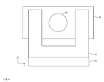
- FIG. 4 is a back view of the light-receiving package for flat-plate mounting 30 according to the embodiment.
- the light-receiving package for flat-plate mounting 30 according to the embodiment is provided with a first subassembly 31 and a second subassembly 32.
- the first subassembly 31 is provided with a photo diode 41 and a retaining holder 42.
- the second subassembly 32 is provided with a rectangular U-shaped concave holder 43 and a flat-plate base 44.
- the photo diode 41 includes a monitor PD 51 mounted on a small-sized CAN-PKG (package).
- the monitor PD 51 is mounted in the small-sized CAN-PKG, constituted of a flat-plate base 54, a cap 52, and the light entering window 53, and sealed airtightly.
- the photo diode 41 can be aligned in the optical module, and stable reception sensitivity can be always obtained.
- An indirect component such as a lens can be mounted in the small-sized CAN-PKG. When the effective diameters of the light entering window 53 and a lens of the small-sized CAN-PKG are controlled, sufficient cross talk to stray light can be secured.
- the light entering window 53 of the small-sized CAN-PKG in which the monitor PD 51 is mounted may be flat glass or lens.
- the light entering window 53 is a predetermined opening. This can suppress entering of stray light and entering of local light inside a module. Consequently, the reception sensitivity with a suppressed noise component can be obtained.
- the photo diode 41 is fixed to the retaining holder 42 for alignment, and the first subassembly 31 is formed.
- the retaining holder 42 is preferably a metal material such as Fe-Ni-Co. In a fixing method, an adhesive, laser welding, or the like may be used.
- the rectangular U-shaped concave holder 43 is fixed at a predetermined position of the flat-plate base 44, and the second subassembly 32 is formed. At this time, the rectangular U-shaped concave holder 43 and the flat-plate base 44 are fixed so that a cut-out side of the rectangular U-shaped concave holder 43 faces above the substrate 11.
- the rectangular U-shaped concave holder 43 is fixed onto the flat-plate base 44 with an adhesive or the like.
- the rectangular U-shaped concave holder 43 is preferably a metal material such as Fe-Ni-Co.
- the flat-plate base 44 is preferably formed of alumina.
- the second subassembly 32 is fixed at a predetermined position on the substrate 11 with an adhesive or the like, for the purpose of retaining the first subassembly 31.
- the surface of the flat-plate base 44 that is mounted on the substrate 11 is a flat surface capable of moving parallel to the substrate surface and can be disposed at a predetermined position on the substrate 11.
- a back surface 45 of the retaining holder 42 that faces the light entering window 53 is brought into contact with a PLC-side flat surface 46 of the rectangular U-shaped concave holder 43 of the second subassembly 32, and optical alignment is performed.
- the PLC-side flat surface 46 on which the back surface 45 of the retaining holder 42 is disposed on the PLC optical demodulator circuit 13 side of a surface of the rectangular U-shaped concave holder 43 having a U-shape is a flat surface
- optical alignment in an x-y plane parallel to a light-receiving surface of the monitor PD 51 can be performed by rubbing the back surface 45 of the retaining holder 42 with the PLC-side flat surface 46 of the rectangular U-shaped concave holder 43.
- the alignment is performed in this plane, spot welding using a YAG laser is performed at a position where predetermined reception sensitivity is obtained, and the retaining holder 42 and the rectangular U-shaped concave holder 43 are fixed, whereby the first subassembly 31 is fixed to the second subassembly 32, and the light-receiving package for flat-plate mounting 30 is mounted on the substrate 11.
- the reception sensitivity of the monitor PD can be made constant.
- the PLC optical demodulator circuit 13 may be connected to the two optical fibers 16. For example, signal light enters the PLC optical demodulator circuit 13 through one of the optical fibers 16, and local light enters the PLC optical demodulator circuit 13 through the other optical fiber 16. In this case, the PLC optical demodulator circuit 13 divides only a portion of the signal light as monitor light and emits the monitor light through the light emitting window 34. At this time, since the local light is dispersed in the PLC optical demodulator circuit 13, stray light of the local light may emit through the light emitting window 34. Thus, a slit is provided on an optical axis of the monitor light divided in the PLC optical demodulator circuit 13 and emitted through the light emitting window 34.
- the light emitting window 34 and the light entering window 53 are each provided with a slit passing the monitor light therethrough and shielding stray light in the waveguide type optical element.
- the slits of the light emitting window 34 and the light entering window 53 are formed by reducing the opening diameters of the light emitting window 34 and the light entering window 53. According to this constitution, entering of local light can be reduced, and sufficient cross talk can be secured.
- the present invention can provide a receiving FE module with a built-in monitor PD, which can make the reception sensitivity constant and perform stabilized operation.
- the present invention is applicable to information and communication industry.
Landscapes
- Physics & Mathematics (AREA)
- General Physics & Mathematics (AREA)
- Optics & Photonics (AREA)
- Engineering & Computer Science (AREA)
- Microelectronics & Electronic Packaging (AREA)
- Optical Couplings Of Light Guides (AREA)
- Light Receiving Elements (AREA)
Abstract
This invention provides a light-receiving package for flat-plate mounting which can make monitor reception sensitivity of an optical signal constant without increasing the size of a module.
The light-receiving package for flat-plate mounting of the present invention is provided with a first subassembly 31 in which a photo diode 41 is fixed to a front surface of a retaining holder 42, a back surface of the retaining holder 42 is a flat surface capable of moving parallel on a plane parallel to a light-receiving surface of the photo diode 41 and a second subassembly 32 which has a rectangular U-shaped concave holder 43 for retaining the retaining holder 42, and a flat-plate base 44 disposed on a substrate 11 and in which a surface of the flat-plate base 44 that is mounted on the substrate 11 is a flat surface capable of moving parallel to a substrate surface, the rectangular U-shaped concave holder 43 and the flat-plate base 44 are fixed, at least one of surfaces of the concave holder 43 having a rectangular U-shape being a flat surface is a flat surface capable of moving parallel to the back surface of the retaining holder 42.
Description
- The present invention relates to a light-receiving package for flat-plate mounting, which is mounted with a monitor PD (PhotoDiode), and an optical module.
- A
conventional monitor PD 102 has a coaxial structure with a fiber, and, as shown inFIG. 6 , an optical signal is tapped to anoptical fiber 103 of anoptical module 101 to connect themonitor PD 102 by fusion bonding and, thus, to monitor an output of the optical signal (for example, see - Patent Literature 1).
-
FIG. 7 shows a conventional example in which themonitor PD 102 is integrated in the optical module 101 (for example, see Patent Literature 2). In the prior art, themonitor PD 102 is in a form in which a PD bare chip is mounted on a carrier such as ceramic. -
- Patent Literature 1:
JP 1996-122582 A - Patent Literature 2:
JP 2002-357743 A - According to the conventional example of Patent Literature 1, since the monitor PD is connected to the middle of the optical fiber of the optical module, the entire module is increased in size, and it is difficult to arrange and store the optical fiber when a board is implemented.
- According to the conventional example of Patent Literature 2, since the PD bare chip is exposed inside the optical module, not only a main optical signal but also a stray light component generated in the optical module are received, and thus it is difficult to stably monitor the optical signal. Further, since the monitor PD is implemented without adjustment, there is a problem that reception sensitivity varies depending on a lot and mounting accuracy.
- Thus, an object of the present invention is to provide a light-receiving package for flat-plate mounting and an optical module which can make reception sensitivity constant without increasing the size of a module. Solution to Problem
- In order to achieve the above object, a light-receiving package for flat-plate mounting of the present invention is provided with a first subassembly which has a photo diode and a retaining holder and in which the photo diode is fixed to a front surface of the retaining holder, a back surface of the retaining holder is a flat surface capable of moving parallel on a plane parallel to a light-receiving surface of the photo diode and a second subassembly which has the rectangular U-shaped concave holder for retaining the retaining holder and a flat-plate base disposed on a substrate and in which a surface of the flat-plate base that is mounted on the substrate is a flat surface capable of moving parallel to a substrate surface, the rectangular U-shaped concave holder and the flat-plate base are fixed so that a cut-out side of the rectangular U-shaped concave holder faces above the substrate, and at least one of surfaces of the concave holder having a rectangular U-shape is a flat surface capable of moving parallel to the back surface of the retaining holder.
- The second subassembly is provided with the flat-plate base, whereby the photo diode can be installed at a desired position on the substrate. The second subassembly is provided with the rectangular U-shaped concave holder, and the first subassembly is provided with the retaining holder, whereby the photo diode can be moved parallel on a surface parallel to the light-receiving surface of the photo diode, and the monitor PD can be fixed at a position where the reception sensitivity of the monitor PD is proper. According to this constitution, the reception sensitivity of the monitor PD can be made constant and stabilized. Accordingly, the light-receiving package for flat-plate mounting of the present invention can make the reception sensitivity constant without increasing the size of a module.
- The optical module of the present invention is provided with a waveguide type optical element which is mounted on the substrate and guides light from an optical fiber and the light-receiving package for flat-plate mounting of the present invention which receives monitor light emitted from the waveguide type optical element after separation of a portion of light propagating through the waveguide type optical element.
- Since the optical module of the present invention is provided with the light-receiving package for flat-plate mounting of the present invention, even if the monitor PD is disposed in the optical module, the reception sensitivity of the monitor PD can be made constant. Accordingly, the optical module of the present invention can make the reception sensitivity constant without increasing the size of a module.
- In the optical module of the present invention, a light emitting window through which the monitor light emits is provided in an end surface of the waveguide type optical element that is connected to the optical fiber, a photo diode of the light-receiving package for flat-plate mounting is provided with a light entering window for the monitor light, and the light emitting window and the light entering window may be arranged to face each other.
- In the optical module of the present invention, since the light emitting window is disposed in the end surface of the waveguide type optical element that is connected to the optical fiber, stray light entering the light entering window can be reduced. Consequently, the optical module of the present invention can monitor signal light accurately.
- In the optical module of the present invention, the waveguide type optical element is connected to two optical fibers, the light emitting window emits monitor light from which a portion of light from one of the optical fibers is devided, and the light emitting window and the light entering window may pass the monitor light therethrough and shield stray light in the waveguide type optical element.
- In the optical module of the present invention, when signal light and local light enter the waveguide type optical element, only the signal light as the monitor light can be extracted from the light emitting window. Since the light emitting window and the light entering window pass the monitor light therethrough and shield the stray light in the waveguide type optical element, only the monitor light from which the signal light is devided can be made enter the monitor PD. According to this constitution, the optical module of the present invention can monitor the signal light accurately.
- The present invention can provide a light-receiving package for flat-plate mounting and an optical module which can make reception sensitivity of a monitor PD constant and stabilize without increasing the size of a module.
-
-
FIG. 1 shows a top view of an optical module according to the present embodiment. -
FIG. 2 shows an A-A' cross-sectional view of the optical module according to the embodiment. -
FIG. 3 is a side view of a light-receiving package for flat-plate mounting according to the embodiment. -
FIG. 4 is a back view of the light-receiving package for flat-plate mounting according to the embodiment. -
FIG. 5 shows an example of a photo diode according to the embodiment. -
FIG. 6 shows a monitor PD mounting example of Patent Literature 1. -
FIG. 7 shows a monitor PD mounting example of Patent Literature 2. - An embodiment of the present invention will be described with reference to the accompanying drawings. The embodiment to be described hereinafter is an example of the invention, and the invention is not limited to the following embodiment. Components denoted by the same reference numerals in the present specification and the drawings mutually denote the same components.
- An optical module according to the present embodiment is an integrated type receiving FE module corresponding to optical phase modulation accompanying a further increase in communication traffic, that is, a DQPSK transmission method or a DP-QPSK transmission method. A PLC optical demodulator circuit used in those transmission methods is called a delay line interferometer DLI or DPOH (Dual Polarization Optical Hybrid), converts a difference in phase state of an optical signal into a difference in light intensity, and is an optical module which receives and demodulates this by a PD capable of detecting only an intensity difference and integrates a high frequency amplifier which current/voltage converts an electrical signal demodulated by the PD to amplify the converted signal and, thus, to output the amplified signal as a high frequency electrical signal.
-
FIGS. 1 and2 show an example of the optical module according to the present embodiment.FIG. 1 is a top view of the optical module according to the embodiment, andFIG. 2 is a side view of the optical module according to the embodiment. The optical module according to the embodiment is provided with asubstrate 11, anoptical semiconductor package 12, a PLCoptical demodulator circuit 13 as a waveguide type optical element, anoptical lens 14, alens retaining holder 17, and a light-receiving package for flat-plate mounting 30. Theoptical semiconductor package 12 is provided with a receiver for demodulation, and the light-receiving package for flat-plate mounting 30 is provided with a monitor PD. - An optical signal transmitted from an
optical fiber 16 enters the PLCoptical demodulator circuit 13. The PLCoptical demodulator circuit 13 is mounted on thesubstrate 11 and guides light from theoptical fiber 16. In the PLCoptical demodulator circuit 13, a waveguide is divided (tapped), and the optical signal is divided into the optical signal travelling toward the receiver for demodulation and an optical signal travelling toward the monitor PD. The optical signal travelling toward the monitor PD is monitor light and is emitted through alight emitting window 34 disposed in an end surface connected to theoptical fiber 16. Thelight emitting window 34 as a PLC light-emitting end is obliquely cut for countermeasure against reflection, and an AR plate is mounted. According to this constitution, reflection as a noise component can be suppressed. - The optical signal for monitor PD reception, that is, monitor light is output through the
light emitting window 34 disposed on the side of afiber input portion 33 and enters the monitor PD in the light-receiving package for flat-plate mounting 30 through alight entering window 53 disposed to face thelight emitting window 34. The monitor PD in the light-receiving package for flat-plate mounting 30 receives the monitor light entering through thelight entering window 53, and optical sensitivity can be obtained. When the monitor PD is mounted on the side of thefiber input portion 33, it is possible to suppress that the monitor PD receives scattered light generated in a PLC substrate. -
FIGS. 3 and4 show an example of the light-receiving package for flat-plate mounting 30.FIG. 3 is a side view of the light-receiving package for flat-plate mounting 30 according to this embodiment, andFIG. 4 is a back view of the light-receiving package for flat-plate mounting 30 according to the embodiment. The light-receiving package for flat-plate mounting 30 according to the embodiment is provided with afirst subassembly 31 and asecond subassembly 32. Thefirst subassembly 31 is provided with aphoto diode 41 and aretaining holder 42. Thesecond subassembly 32 is provided with a rectangular U-shapedconcave holder 43 and a flat-plate base 44. - In
FIG. 5 , an example of aphoto diode 41 is shown. Thephoto diode 41 includes amonitor PD 51 mounted on a small-sized CAN-PKG (package). Themonitor PD 51 is mounted in the small-sized CAN-PKG, constituted of a flat-plate base 54, acap 52, and thelight entering window 53, and sealed airtightly. Thus, even if themonitor PD 51 is mounted in an unsealed optical module, stabilized operation can be performed. Thephoto diode 41 can be aligned in the optical module, and stable reception sensitivity can be always obtained. An indirect component such as a lens can be mounted in the small-sized CAN-PKG. When the effective diameters of thelight entering window 53 and a lens of the small-sized CAN-PKG are controlled, sufficient cross talk to stray light can be secured. - The
light entering window 53 of the small-sized CAN-PKG in which themonitor PD 51 is mounted may be flat glass or lens. Thelight entering window 53 is a predetermined opening. This can suppress entering of stray light and entering of local light inside a module. Consequently, the reception sensitivity with a suppressed noise component can be obtained. - In a mounting structure, first, the
photo diode 41 is fixed to the retainingholder 42 for alignment, and thefirst subassembly 31 is formed. The retainingholder 42 is preferably a metal material such as Fe-Ni-Co. In a fixing method, an adhesive, laser welding, or the like may be used. - Then, the rectangular U-shaped
concave holder 43 is fixed at a predetermined position of the flat-plate base 44, and thesecond subassembly 32 is formed. At this time, the rectangular U-shapedconcave holder 43 and the flat-plate base 44 are fixed so that a cut-out side of the rectangular U-shapedconcave holder 43 faces above thesubstrate 11. The rectangular U-shapedconcave holder 43 is fixed onto the flat-plate base 44 with an adhesive or the like. The rectangular U-shapedconcave holder 43 is preferably a metal material such as Fe-Ni-Co. The flat-plate base 44 is preferably formed of alumina. - The
second subassembly 32 is fixed at a predetermined position on thesubstrate 11 with an adhesive or the like, for the purpose of retaining thefirst subassembly 31. The surface of the flat-plate base 44 that is mounted on thesubstrate 11 is a flat surface capable of moving parallel to the substrate surface and can be disposed at a predetermined position on thesubstrate 11. - Then, in the optical module a
back surface 45 of the retainingholder 42 that faces thelight entering window 53 is brought into contact with a PLC-sideflat surface 46 of the rectangular U-shapedconcave holder 43 of thesecond subassembly 32, and optical alignment is performed. Since the PLC-sideflat surface 46 on which theback surface 45 of the retainingholder 42 is disposed on the PLCoptical demodulator circuit 13 side of a surface of the rectangular U-shapedconcave holder 43 having a U-shape is a flat surface, optical alignment in an x-y plane parallel to a light-receiving surface of themonitor PD 51 can be performed by rubbing theback surface 45 of the retainingholder 42 with the PLC-sideflat surface 46 of the rectangular U-shapedconcave holder 43. The alignment is performed in this plane, spot welding using a YAG laser is performed at a position where predetermined reception sensitivity is obtained, and the retainingholder 42 and the rectangular U-shapedconcave holder 43 are fixed, whereby thefirst subassembly 31 is fixed to thesecond subassembly 32, and the light-receiving package for flat-plate mounting 30 is mounted on thesubstrate 11. According to this constitution, the reception sensitivity of the monitor PD can be made constant. - Electrical connection is performed from a
lead 55, output from the small-type CAN-PKG mounted with themonitor PD 51, to aceramic terminal 19 inside the optical module by wire bonding. - The PLC
optical demodulator circuit 13 may be connected to the twooptical fibers 16. For example, signal light enters the PLCoptical demodulator circuit 13 through one of theoptical fibers 16, and local light enters the PLCoptical demodulator circuit 13 through the otheroptical fiber 16. In this case, the PLCoptical demodulator circuit 13 divides only a portion of the signal light as monitor light and emits the monitor light through thelight emitting window 34. At this time, since the local light is dispersed in the PLCoptical demodulator circuit 13, stray light of the local light may emit through thelight emitting window 34. Thus, a slit is provided on an optical axis of the monitor light divided in the PLCoptical demodulator circuit 13 and emitted through thelight emitting window 34. For example, thelight emitting window 34 and thelight entering window 53 are each provided with a slit passing the monitor light therethrough and shielding stray light in the waveguide type optical element. The slits of thelight emitting window 34 and thelight entering window 53 are formed by reducing the opening diameters of thelight emitting window 34 and thelight entering window 53. According to this constitution, entering of local light can be reduced, and sufficient cross talk can be secured. - As described above, the present invention can provide a receiving FE module with a built-in monitor PD, which can make the reception sensitivity constant and perform stabilized operation.
- The present invention is applicable to information and communication industry.
-
- 11: substrate
- 12: optical semiconductor package
- 13: PLC optical demodulator circuit
- 14: optical lens
- 16: optical fiber
- 17: lens retaining holder
- 18: flange
- 19: ceramic terminal
- 30: light-receiving package for flat-plate mounting
- 31: first subassembly
- 32: second subassembly
- 33: fiber input portion
- 34: light emitting window
- 41: photo diode
- 42: retaining holder
- 43: a rectangular U-shaped concave holder
- 44: flat-plate base
- 45: back surface of retaining holder
- 46: PLC-side flat surface of a rectangular U-shaped concave
- holder
- 51: monitor PD
- 52: cap
- 53: light entering window
- 54: flat-plate base
- 55: lead
- 101: optical module
- 102: monitor PD
- 103: optical fiber
- 104: connector
- 105: LD
Claims (4)
- A light-receiving package for flat-plate mounting comprising:a first subassembly having a photo diode and a retaining holder, the photo diode being fixed to a front surface of the retaining holder, and a back surface of the retaining holder being a flat surface capable of moving parallel on a plane parallel to a light-receiving surface of the photo diode; anda second subassembly having a rectangular U-shaped concave holder for retaining the retaining holder and a flat-plate base disposed on a substrate, a surface of the flat-plate base that is mounted on the substrate being a flat surface capable of moving parallel to a substrate surface, the rectangular U-shaped concave holder and the flat-plate base being fixed so that a cut-out side of the rectangular U-shaped concave holder faces above the substrate, and at least one of surfaces of the concave holder having a rectangular U-shape being a flat surface capable of moving parallel to the back surface of the retaining holder.
- An optical module comprising:a waveguide type optical element mounted on the substrate and guides light from an optical fiber; andthe light-receiving package for flat-plate mounting according to claim 1, which receives monitor light emitted from the waveguide type optical element after separation of a portion of light propagating through the waveguide type optical element.
- The optical module according to claim 2,
wherein the waveguide type optical element comprises a light emitting window, through which the monitor light emits, in an end surface connected to the optical fiber,
a photo diode of the light-receiving package for flat-plate mounting comprises a light entering window for the monitor light, and
the light emitting window and the light entering window are arranged to face each other. - The optical module according to claim 3,
wherein the waveguide type optical element is connected to two optical fibers,
monitor light from which a portion of light from one of the optical fibers is divided is emitted through the light emitting window, and
the light emitting window and the light entering window have a slit passing the monitor light therethrough and shielding stray light in the waveguide type optical element.
Applications Claiming Priority (2)
| Application Number | Priority Date | Filing Date | Title |
|---|---|---|---|
| JP2012000363A JP2013140259A (en) | 2012-01-05 | 2012-01-05 | Receiving package for flat plate arrangement, optical module, and manufacturing method of receiving package for flat plate arrangement |
| PCT/JP2012/081396 WO2013103063A1 (en) | 2012-01-05 | 2012-12-04 | Light-receiving package for flat-plate mounting, and optical module |
Publications (2)
| Publication Number | Publication Date |
|---|---|
| EP2801852A1 true EP2801852A1 (en) | 2014-11-12 |
| EP2801852A4 EP2801852A4 (en) | 2015-10-07 |
Family
ID=48722317
Family Applications (1)
| Application Number | Title | Priority Date | Filing Date |
|---|---|---|---|
| EP12864605.6A Withdrawn EP2801852A4 (en) | 2012-01-05 | 2012-12-04 | FLAT RECEPTION LIGHT RECEPTION HOUSING, AND OPTICAL MODULE |
Country Status (5)
| Country | Link |
|---|---|
| US (1) | US9182559B2 (en) |
| EP (1) | EP2801852A4 (en) |
| JP (1) | JP2013140259A (en) |
| CN (2) | CN203164479U (en) |
| WO (1) | WO2013103063A1 (en) |
Cited By (1)
| Publication number | Priority date | Publication date | Assignee | Title |
|---|---|---|---|---|
| US20220099560A1 (en) * | 2016-06-15 | 2022-03-31 | Sorin Group Italia S.R.L. | Methods and devices for monitoring blood |
Families Citing this family (7)
| Publication number | Priority date | Publication date | Assignee | Title |
|---|---|---|---|---|
| JP2013140259A (en) * | 2012-01-05 | 2013-07-18 | Ntt Electornics Corp | Receiving package for flat plate arrangement, optical module, and manufacturing method of receiving package for flat plate arrangement |
| JP2015014689A (en) * | 2013-07-04 | 2015-01-22 | Nttエレクトロニクス株式会社 | Light receiving package for flat plate arrangement and optical module |
| WO2015040953A1 (en) * | 2013-09-17 | 2015-03-26 | 株式会社フジクラ | Optical transmission module and method for assembling optical transmission module |
| US20170063464A1 (en) | 2015-08-27 | 2017-03-02 | Applied Optoelectronics, Inc. | Multi-channel transmitter optical subassembly (tosa) with opposing placement of transistor outline (to) can laser packages |
| US20170063465A1 (en) * | 2015-08-27 | 2017-03-02 | Applied Optoelectronics, Inc. | Techniques for reducing the footprint of a multi-channel transmitter optical subassembly (tosa) within an optical transceiver housing |
| WO2017203785A1 (en) * | 2016-05-23 | 2017-11-30 | オリンパス株式会社 | Optical signal transmission module |
| CN111865429B (en) * | 2019-04-30 | 2022-05-27 | 深圳市聚飞光电股份有限公司 | Photoelectric receiver and manufacturing method thereof |
Family Cites Families (14)
| Publication number | Priority date | Publication date | Assignee | Title |
|---|---|---|---|---|
| JPS62169487A (en) * | 1986-01-22 | 1987-07-25 | Hitachi Ltd | Photoelectronic device |
| JPH01241504A (en) * | 1988-03-23 | 1989-09-26 | Hitachi Ltd | Assembly method of composite optical device |
| JPH0450903A (en) * | 1990-06-15 | 1992-02-19 | Fujitsu Ltd | Semiconductor laser module |
| JPH05333248A (en) * | 1992-06-01 | 1993-12-17 | Hitachi Cable Ltd | Wavelength division multiplex system transmit-receive module and optical transmitter using same |
| JPH08122582A (en) | 1994-10-28 | 1996-05-17 | Hitachi Cable Ltd | PD module |
| JP2001249241A (en) * | 2000-03-06 | 2001-09-14 | Hitachi Cable Ltd | Waveguide type bidirectional optical transmission module |
| JP4583662B2 (en) | 2001-06-01 | 2010-11-17 | 三菱電機株式会社 | Optical module package and manufacturing method thereof |
| KR100416688B1 (en) | 2001-11-08 | 2004-01-31 | 주식회사 한택 | Optical fiber block integrated with photo device |
| US7266270B2 (en) * | 2002-03-15 | 2007-09-04 | Tessera North America | Waveguide to waveguide monitor |
| CN1720473A (en) * | 2002-11-08 | 2006-01-11 | Tdk株式会社 | Optical module and method for manufacturing same |
| JP4265308B2 (en) | 2003-06-27 | 2009-05-20 | 日本電気株式会社 | Optical element holder and optical communication module using the same |
| WO2007108508A1 (en) * | 2006-03-22 | 2007-09-27 | The Furukawa Electric Co., Ltd. | Optical module |
| JP4913526B2 (en) * | 2006-10-04 | 2012-04-11 | 古河電気工業株式会社 | Manufacturing method of optical module |
| JP2013140259A (en) * | 2012-01-05 | 2013-07-18 | Ntt Electornics Corp | Receiving package for flat plate arrangement, optical module, and manufacturing method of receiving package for flat plate arrangement |
-
2012
- 2012-01-05 JP JP2012000363A patent/JP2013140259A/en active Pending
- 2012-12-04 WO PCT/JP2012/081396 patent/WO2013103063A1/en not_active Ceased
- 2012-12-04 EP EP12864605.6A patent/EP2801852A4/en not_active Withdrawn
- 2012-12-04 US US14/370,673 patent/US9182559B2/en active Active
-
2013
- 2013-01-04 CN CN2013200007374U patent/CN203164479U/en not_active Expired - Fee Related
- 2013-01-04 CN CN2013100005585A patent/CN103199941A/en active Pending
Cited By (3)
| Publication number | Priority date | Publication date | Assignee | Title |
|---|---|---|---|---|
| US20220099560A1 (en) * | 2016-06-15 | 2022-03-31 | Sorin Group Italia S.R.L. | Methods and devices for monitoring blood |
| US11994460B2 (en) * | 2016-06-15 | 2024-05-28 | Sorin Group Italia S.R.L. | Methods and devices for monitoring blood |
| US12560528B2 (en) | 2016-06-15 | 2026-02-24 | Sorin Group Italia S.R.L. | Methods and devices for monitoring blood |
Also Published As
| Publication number | Publication date |
|---|---|
| EP2801852A4 (en) | 2015-10-07 |
| WO2013103063A1 (en) | 2013-07-11 |
| US9182559B2 (en) | 2015-11-10 |
| CN203164479U (en) | 2013-08-28 |
| CN103199941A (en) | 2013-07-10 |
| JP2013140259A (en) | 2013-07-18 |
| US20140369644A1 (en) | 2014-12-18 |
Similar Documents
| Publication | Publication Date | Title |
|---|---|---|
| US9182559B2 (en) | Light-receiving package for flat-plate mounting, and optical module | |
| US8121484B2 (en) | Bi-direction optical module installing light-emitting device and light-receiving device in signal package | |
| JP6046475B2 (en) | Improved transistor outline (TO) -CAN assembly for use in optical communications | |
| US9134490B2 (en) | Passive alignment multichannel parallel optical system | |
| US20170045697A1 (en) | Photonic interface for electronic circuit | |
| US20150183060A1 (en) | Method of manufacturing an optical module | |
| JP6221263B2 (en) | Optical modulator module | |
| US8907266B2 (en) | Light-receiving device array, optical receiver module, and optical transceiver | |
| JP2002064212A (en) | Optical receiving module | |
| US9383528B2 (en) | Light-receiving module | |
| KR100526505B1 (en) | Structure of coupling up optical device to optical waveguide and method for coupling arrangement using the same | |
| US20180341073A1 (en) | Single-Fiber Bidirectional Sub Assembly | |
| US20080187321A1 (en) | Optical transceiver module | |
| JP5649422B2 (en) | Optical device manufacturing method | |
| CN204203506U (en) | Flat panel configurations optical fiber receive module and optical module | |
| JP2006345474A (en) | Optical transceiver module | |
| US10126510B2 (en) | Detection device | |
| JP6413340B2 (en) | Optical module manufacturing method and optical module manufacturing apparatus | |
| CN108292020A (en) | Optical receiver and assembly method thereof | |
| US20050169634A1 (en) | Bi-directional optical transceiver module and bi-directional optical transceiver package using the same | |
| KR101361069B1 (en) | Optical subassembly | |
| JP3348644B2 (en) | Optical receiving module and optical transmitting / receiving module | |
| JP2012118292A (en) | Optical device | |
| CN113267851A (en) | Optical communication module | |
| JP2016218203A (en) | Optical module |
Legal Events
| Date | Code | Title | Description |
|---|---|---|---|
| PUAI | Public reference made under article 153(3) epc to a published international application that has entered the european phase |
Free format text: ORIGINAL CODE: 0009012 |
|
| 17P | Request for examination filed |
Effective date: 20140805 |
|
| AK | Designated contracting states |
Kind code of ref document: A1 Designated state(s): AL AT BE BG CH CY CZ DE DK EE ES FI FR GB GR HR HU IE IS IT LI LT LU LV MC MK MT NL NO PL PT RO RS SE SI SK SM TR |
|
| DAX | Request for extension of the european patent (deleted) | ||
| RA4 | Supplementary search report drawn up and despatched (corrected) |
Effective date: 20150908 |
|
| RIC1 | Information provided on ipc code assigned before grant |
Ipc: G02B 6/42 20060101AFI20150902BHEP |
|
| STAA | Information on the status of an ep patent application or granted ep patent |
Free format text: STATUS: THE APPLICATION IS DEEMED TO BE WITHDRAWN |
|
| 18D | Application deemed to be withdrawn |
Effective date: 20160406 |