EP2799843A1 - Spfs measurement sensor chip, spfs measurement method employing spfs measurement sensor chip, and spfs measurement device comprising spfs measurement sensor chip - Google Patents
Spfs measurement sensor chip, spfs measurement method employing spfs measurement sensor chip, and spfs measurement device comprising spfs measurement sensor chip Download PDFInfo
- Publication number
- EP2799843A1 EP2799843A1 EP12862962.3A EP12862962A EP2799843A1 EP 2799843 A1 EP2799843 A1 EP 2799843A1 EP 12862962 A EP12862962 A EP 12862962A EP 2799843 A1 EP2799843 A1 EP 2799843A1
- Authority
- EP
- European Patent Office
- Prior art keywords
- spfs measurement
- dielectric member
- sensor chip
- thin film
- metal thin
- Prior art date
- Legal status (The legal status is an assumption and is not a legal conclusion. Google has not performed a legal analysis and makes no representation as to the accuracy of the status listed.)
- Granted
Links
Images





Classifications
-
- G—PHYSICS
- G01—MEASURING; TESTING
- G01N—INVESTIGATING OR ANALYSING MATERIALS BY DETERMINING THEIR CHEMICAL OR PHYSICAL PROPERTIES
- G01N21/00—Investigating or analysing materials by the use of optical means, i.e. using sub-millimetre waves, infrared, visible or ultraviolet light
- G01N21/62—Systems in which the material investigated is excited whereby it emits light or causes a change in wavelength of the incident light
- G01N21/63—Systems in which the material investigated is excited whereby it emits light or causes a change in wavelength of the incident light optically excited
- G01N21/64—Fluorescence; Phosphorescence
- G01N21/645—Specially adapted constructive features of fluorimeters
- G01N21/648—Specially adapted constructive features of fluorimeters using evanescent coupling or surface plasmon coupling for the excitation of fluorescence
-
- G—PHYSICS
- G01—MEASURING; TESTING
- G01N—INVESTIGATING OR ANALYSING MATERIALS BY DETERMINING THEIR CHEMICAL OR PHYSICAL PROPERTIES
- G01N33/00—Investigating or analysing materials by specific methods not covered by groups G01N1/00 - G01N31/00
- G01N33/48—Biological material, e.g. blood, urine; Haemocytometers
- G01N33/50—Chemical analysis of biological material, e.g. blood, urine; Testing involving biospecific ligand binding methods; Immunological testing
- G01N33/53—Immunoassay; Biospecific binding assay; Materials therefor
- G01N33/543—Immunoassay; Biospecific binding assay; Materials therefor with an insoluble carrier for immobilising immunochemicals
- G01N33/54366—Apparatus specially adapted for solid-phase testing
- G01N33/54373—Apparatus specially adapted for solid-phase testing involving physiochemical end-point determination, e.g. wave-guides, FETS, gratings
-
- G—PHYSICS
- G01—MEASURING; TESTING
- G01N—INVESTIGATING OR ANALYSING MATERIALS BY DETERMINING THEIR CHEMICAL OR PHYSICAL PROPERTIES
- G01N21/00—Investigating or analysing materials by the use of optical means, i.e. using sub-millimetre waves, infrared, visible or ultraviolet light
- G01N21/62—Systems in which the material investigated is excited whereby it emits light or causes a change in wavelength of the incident light
- G01N21/63—Systems in which the material investigated is excited whereby it emits light or causes a change in wavelength of the incident light optically excited
- G01N21/64—Fluorescence; Phosphorescence
- G01N2021/6417—Spectrofluorimetric devices
Definitions
- the present invention relates to a sensor chip for SPFS measurement that is used for a surface plasmon-field enhanced fluorescence spectrometry device using a surface plasmon-filed enhanced fluorescence spectroscopy (SPFS; Surface Plasmon-field enhanced Fluorescence Spectroscopy) (hereinafter referred to simply as "SPFS”) in the field of medical care or biotechnology, for example, and an SPFS measurement method using the sensor chip for SPFS measurement, and an SPFS measurement device equipped with the sensor chip for SPFS measurement.
- SPFS surface plasmon-field enhanced fluorescence spectroscopy
- SPFS surface plasmon-field enhanced fluorescence spectroscopy
- the surface plasmon-field enhanced fluorescence spectroscopy is a method in which the evanescent wave generated by incoming of excitation light under the attenuated total reflection (ATR; attenuated total reflectance) conditions is resonated with surface plasmons on the surface of a metal thin film, and thereby, localized electric field, which is enhanced several tens to several hundreds of times, can be formed on the surface of the metal thin film; a fluorescent substance with which a captured analyte is conjugated (labeled) is set in this enhanced localized electric field; the fluorescence of the fluorescent substance is efficiently excited; and, by observing this fluorescence, a very slight amount or a very low concentration of an analyte is detected.
- ATR attenuated total reflection
- Patent Document 1 Japanese Patent No. 4689907
- a sensor chip for SPFS measurement that is used for such an SPFS device has a dielectric member constituting a prism, and, on the top surface of this dielectric member, a metal thin film has been formed.
- Patent Document 1 Japanese Patent No. 4689907
- a gate for introducing a resin is set in the bottom part of the dielectric and injection molding is carried out.
- the sensor chip for SPFS measurement has a problem that, with regard to the S/N ratio which is a ratio of a signal to be detected to the background noise in the fluorescence measurement, the S/N ratios after leaving in the environment ("finalS/N") are decreased as compared to the initial S/N ratios (“iniS/N”) and this hinders a highly precise and accurate SPFS measurement.
- S/N ratio which is a ratio of a signal to be detected to the background noise in the fluorescence measurement
- the sensor chip for SPFS measurement has a problem that the values of the CV, coefficient of variation, are not stable and this hinders a highly precise and accurate SPFS measurement.
- an object of the present invention is to provide a sensor chip for SPFS measurement, by which, irrespective of environmental conditions, the variation of properties of the signal, the noise, the detection sensitivity and so on is small, and the quantitative property can be ensured, and a highly precise and accurate SPFS measurement can be carried out, and an SPFS measurement method using the sensor chip for SPFS measurement, and an SPFS measurement device equipped with the sensor chip for SPFS measurement.
- the sensor chip for SPFS measurement of the present invention is a sensor chip for SPFS measurement which has a dielectric member constituting a prism, said dielectric member having been produced by carrying out injection molding of a resin, characterized in that said sensor chip for SPFS measurement has been arranged such that a resin inlet is set on one side end surface of the dielectric member, said one side end surface intersecting with an excitation light incoming surface of said dielectric member, a metal thin film-formed surface of said dielectric member, and a reflected light outgoing surface through which a reflected light that comes in through said excitation light incoming surface and is reflected by the metal thin film-formed surface of said dielectric member goes out; and, when viewing from the metal thin film-formed surface side of said dielectric member and taking as b the distance of the side end surface position of said resin inlet to the position on said metal thin film-formed surface that is farthest from the side end surface position of said resin in
- the SPFS measurement method of the present invention is characterized in that a sensor chip for SPFS measurement which has a dielectric member constituting a prism, said dielectric member having been produced by carrying out injection molding of a resin, wherein a resin inlet is set on one side end surface of the dielectric member, said one side end surface intersecting with an excitation light incoming surface of said dielectric member, a metal thin film-formed surface of said dielectric member, and a reflected light outgoing surface through which a reflected light that comes in through said excitation light incoming surface and is reflected by the metal thin film-formed surface of said dielectric member goes out, is used; when viewing from the metal thin film-formed surface side of said dielectric member and taking as b the distance of the side end surface position of said resin inlet to the position on said metal thin film-formed surface that is farthest from the side end surface position of said resin inlet, an excitation light is irradiated to at least a portion of a metal thin film from the side where said dielectric member exists,
- the present invention is characterized in that, on the metal thin film-formed surface of said dielectric member, a channel into which a specimen can be introduced has been formed.
- a channel into which a specimen can be introduced has been formed, and therefore, if a sample solution containing a specimen (an analyte) to be detected is made to flow in this channel, then the fluorescent substance with which the analyte captured in the vicinity of the metal thin film is conjugated (labeled) is efficiently excited, and, by observing this fluorescence, a very slight amount or a very low concentration of an analyte can be detected.
- the present invention is characterized by having been arranged such that, in said channel, said ligand immobilization part has been formed, and the direction of the flow in said channel is parallel to the directions of said excitation light incoming surface and said reflected light outgoing surface of said dielectric member.
- the sample solution will flow in a direction parallel to the excitation light incoming surface and the reflected light outgoing surface of the dielectric member, and an analyte can be reliably captured in the ligand immobilization part having been formed in the channel.
- the fluorescent substance with which the analyte captured in the vicinity of the metal thin film is conjugated (labeled) is efficiently excited, and, by observing this fluorescence, a very slight amount or a very low concentration of an analyte can be detected.
- the present invention is characterized in that, on said sensor chip for SPFS measurement, positioning and fixing parts to carry out positioning and fixing of the sensor chip for SPFS measurement in an SPFS measurement device with which detection is carried out are provided.
- the present invention is characterized in that said positioning and fixing parts have been formed in a channel lid member equipped on said dielectric member.
- the present invention is characterized in that said positioning and fixing parts have been formed in said dielectric member.
- the SPFS measurement device of the present invention is characterized by being equipped with the sensor chip for SPFS measurement according to any one of the preceding paragraphs.
- the present invention irrespective of environmental conditions, the variation of properties of the signal, the noise, the detection sensitivity and so on is small, and the quantitative property can be ensured, and a highly precise and accurate SPFS measurement can be carried out.
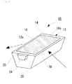
- Fig. 1 is a perspective view of a sensor chip for SPFS measurement of the present invention
- Fig. 2 is a top view of the sensor chip for SPFS measurement of Fig. 1
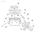
- Fig. 3 is a schematic view illustrating the outline of the evaluation method that was carried out using the sensor chip for SPFS measurement of Fig. 1
- Fig. 4 is a partially enlarged cross-sectional view for explaining the outline of the sensor chip for SPFS measurement of Fig. 3
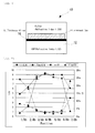
- Fig. 5 is a graph showing the results of the evaluation method.
- the sensor chip 10 for SPFS measurement of this example is a sensor chip for SPFS measurement that is used for a surface plasmon-field enhanced fluorescence spectrometry device using a surface plasmon-field enhanced fluorescence spectroscopy (SPFS; Surface Plasmon-field enhanced Fluorescence Spectroscopy).
- SPFS Surface Plasmon-field enhanced Fluorescence Spectroscopy
- the sensor chip 10 for SPFS measurement has a dielectric member 12 constituting a dielectric member body and constituting a prism whose shape is a hexahedron having a cross section of a substantially trapezoidal shape (a shape of a truncated quadrangular pyramid), and the horizontal top surface of this dielectric member 12 constitutes a metal thin film-formed surface 14 on which a metal thin film 16 has been formed.
- the sensor chip 10 for SPFS measurement is comprised of this dielectric member 12 and the metal thin film 16 which has been formed on the metal thin film-formed surface 14 of the dielectric member 12.
- one side surface which is a lower part of the dielectric member 12 forms an excitation light incoming surface 18 through which an excitation light from a light source not shown comes in as indicated by the arrow in Fig. 1 .
- another side surface which is a lower part of the dielectric member 12 forms a reflected light outgoing surface 20 through which a reflected light reflected by the metal thin film 16 goes out as indicated by the arrow in Fig. 1 .
- a light receiving means not shown that is set on the side of said another side surface which is a lower part of the dielectric member 12 receives the reflected light reflected by the metal thin film 16.
- the material of the dielectric member 12 is at least formed from a material optically transparent to an excitation light, and, from the standpoint of providing a sensor chip 10 for SPFS measurement that is inexpensive and has an excellent handling property, is formed from a resin material by injection molding.
- the resin material from which the dielectric member 12 is formed for example, a polyester such as polyethylene terephthalate (PET), polyethylene naphthalate and the like, a polyolefin such as polyethylene (PE), polypropylene (PP) and the like, a polycycloolefin such as a cycloolefin copolymer (COC), a cycloolefin polymer (COP) and the like, a vinyl resin such as polyvinyl chloride, polyvinylidene chloride and the like, polystyrene, polyether ether ketone (PEEK), polysulfone (PSF), polyether sulfone (PES), polycarbonate (PC), polyamide, polyimide, acrylic resin, triacetylcellulose (TAC), or the like can be used.
- PET polyethylene terephthalate
- PE polyethylene
- PP polypropylene
- a polycycloolefin such as a cycloolef
- a resin inlet (gate) 24 is set on one side end surface 22 of the dielectric member 12, said one side end surface 22 intersecting with the excitation light incoming surface 18 of the dielectric member 12, the metal thin film-formed surface 14 of the dielectric member 12, and the reflected light outgoing surface 20; and injection molding of a resin material is carried out to produce a dielectric member 12.
- intersect is intended to include not only cases of intersecting substantially perpendicularly, but also cases of intersecting at a certain angle, and is not limited.
- a dielectric member 12 having dimensions of 25 mm length x 8 mm width x 3 mm height (Refractive Index: 1.52) was produced by injection molding.
- a metal thin film 16 having a thickness of 41 nm and comprised of gold was formed on a metal thin film-formed surface 14 of this dielectric member 12.
- a plate material (a lid) 13 having a thickness of 2 mm which constitutes a channel lid member 44 and is made of PMMA (polymethyl methacrylate resin) was bonded onto the surface of the sensor chip 10 for SPFS measurement to form a channel 46.
- a laser light (Wavelength: 635 nm) was passed from a light source 26 through a wavelength separation filter (manufactured by Optical Coatings Japan) 28 and a deflecting plate 30; the light source 26 was fixed such that the angle of incidence of the laser light to the metal thin film 16 of the sensor chip 10 for SPFS measurement was an optimal angle; and thereafter, an excitation light by the light source 26 was irradiated to the sensor chip 10 for SPFS measurement.
- a wavelength separation filter manufactured by Optical Coatings Japan
- Fig. 4 schematically illustrates a sensor chip for SPFS measurement. Evaluation of S/N ratios was carried out not in a system in which a dye was fixed on the gold film surface as shown in Fig. 4 , but in a system in which the entire channel was filled with a buffer containing a dye.
- a measurement buffer (a "Tris-Buffered Saline (TBS)" buffer) was made to flow in the channel.
- a dye containing buffer (a TBS buffer containing an "Alexa Fluor 647" reactive dye) was made to flow in the channel.
- After leaving in Environment (“final”): After leaving a channel formed chip in the environment, i.e., after leaving in an environment of 60°C and 80% by mass for 240 hours and thereafter leaving in a room temperature environment for 24 hours, measurement of a signal and the background noise was carried out.
- the material of the metal thin film 16 is not particularly limited, but is preferably comprised of at least one metal selected from the group consisting of gold, silver, aluminum, copper and platinum, more preferably comprised of gold, and may be comprised of an alloy of these metals.
- metals are suitable as a metal thin film 16, because they are stable to oxidization and electric field enhancement by surface plasmon light (compression wave) is increased as described below.
- the method for forming a metal thin film 16 is not particularly limited, and examples thereof include, for example, a sputtering method, a vapor deposition method (such as a resistance heating vapor deposition method, an electron beam vapor deposition method and the like), an electrolytic plating method, an electroless plating method, and so on. It is desirable to preferably use a sputtering method or a vapor deposition method, since the thin film forming conditions thereof are easy to control.
- the thickness of a metal thin film 16 is not particularly limited, but preferably it is desirable that the thickness be within the ranges of: in case of gold, from 5 to 500 nm; in case of silver, from 5 to 500 nm; in case of aluminum, from 5 to 500 nm; in case of copper, from 5 to 500 nm; in case of platinum, from 5 to 500 nm; and in case of an alloy thereof, from 5 to 500 nm.
- the thickness be within the ranges of: in case of gold, from 20 to 70 nm; in case of silver, from 20 to 70 nm; in case of aluminum, from 10 to 50 nm; in case of copper, from 20 to 70 nm; in case of platinum, from 20 to 70 nm; and in case of an alloy thereof, from 10 to 70 nm.
- the thickness of a metal thin film 16 is within the above-described ranges, then surface plasmon light (compression wave) will be easily generated, therefore these ranges are suitable.
- the shape thereof is not particularly limited.
- a sensor chip 10 for SPFS measurement having been arranged like this is used as a sensor chip 10 for an SPFS measurement device.
- a solution containing a ligand that will specifically bind to an analyte to be detected is made to flow on a metal thin film 16 to immobilize the ligand onto the metal thin film 16, and thereafter, washing is carried out.
- the term "sensor chip 10 for SPFS measurement” includes not only those in the state after carrying out immobilization of a ligand onto a metal thin film 16 like this, but also those in the state before carrying out immobilization of a ligand onto a metal thin film 16.
- sample solution containing an analyte conjugated (labeled) with a fluorescent substance is made to flow on the metal thin film 16 to allow it to specifically bind to the ligand on the metal thin film 16, and thereafter, washing is carried out.
- a sample solution to be used here is a solution that has been prepared using a specimen, and examples thereof include, for example, those that have been obtained by mixing a specimen and a reagent(s) to carry out a treatment for making a fluorescent substance bind to an analyte contained in the specimen.
- Examples of such a sample include blood, serum, plasma, urine, snivel, saliva, stool, coelomic fluid (spinal fluid, ascitic fluid, pleural fluid, or the like), and so on.
- the analyte contained in the specimen examples include, for example, nucleic acids (DNAs, RNAs, polynucleotides, oligonucleotides, PNAs (peptide nucleic acids) and the like which may be either single-stranded or double-stranded, or nucleosides, nucleotides and modified molecules thereof), proteins (polypeptides, oligopeptides, and the like), amino acids (including modified amino acids), carbohydrates (oligosaccharides, polysaccharides, sugar chains, and the like), lipids, or modified molecules and complexes thereof, and so on.
- the analyte contained in the specimen may be a carcinoembryonic antigen such as AFP ( ⁇ -fetoprotein), a tumor marker, a signal transducer, a hormone, or the like, and is not particularly limited.
- excitation light P1 is made to come in through an excitation light incoming surface 18 of the dielectric member 12 at an incidence angle of ⁇ 1 relative to the excitation light incoming surface 18 and refract, and the light is irradiated as excitation light P2 to a metal thin film 16 on the top surface of the dielectric member 12 at an incident angle of ⁇ satisfying the total reflection conditions (at an incident angle of a certain angle (resonance angle)).
- reflected light P3 reflected by the metal thin film 16 is refracted on a reflected light outgoing surface 20 formed on another side surface which is a lower part of the dielectric member 12 at a certain angle ⁇ 2, and the light is received as reflected light P4 by a light receiving means not shown that is set on the side of said another side surface which is a lower part of the dielectric member 12. In this way, whether the angle is the predefined incident angle ⁇ satisfying the total reflection conditions or not can be confirmed.
- a light receiving sensor 36 such as a photomultiplier (PMT), a CCD, or the like, is set above the sensor chip 10 for SPFS measurement.
- PMT photomultiplier
- a light collecting means 32 to efficiently collect the light of the fluorescence, and a wavelength separation filter 34 to remove the lights other than the fluorescence and select only the fluorescence are set as shown in Fig. 3 .
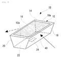
- Fig. 6 is a perspective view of a sensor chip for SPFS measurement of Comparative Example 1;
- Fig. 7 is a top view of the sensor chip for SPFS measurement of Fig. 6 ;
- Fig. 8 is a bottom view of the sensor chip for SPFS measurement of Fig. 6 ;
- Fig. 9 is a graph showing the results of the evaluation method.
- a sensor chip 10 for SPFS measurement was produced in the same manner as in the evaluation test described above. However, as shown in Fig. 6 and Fig. 8 , a resin inlet (gate) 24 is set in the bottom part 40 of a dielectric member 12.
- finalS/N are decreased as compared to the initial S/N ratios ("iniS/N") and this hinders a highly precise and accurate SPFS measurement is found.
- the sensor chip for SPFS measurement has a problem that the values of the CV, coefficient of variation, are not stable and this hinders a highly precise and accurate SPFS measurement.
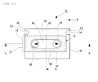
- Fig. 10 is a top view of a sensor chip 10 for SPFS measurement of another example of the present invention
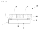
- Fig. 11 is a cross-sectional view taken along the line A-A in the sensor chip 10 for SPFS measurement of Fig. 10
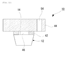
- Fig. 12 is a cross-sectional view taken along the line B-B in the sensor chip 10 for SPFS measurement of Fig. 10 .
- composition of the sensor chip 10 for SPFS measurement of this example is basically the same as that of the sensor chip 10 for SPFS measurement shown in Figs. 1 to 5 , the same composition member is numbered with the same reference number, and the detailed description thereof is omitted.
- the sensor chip 10 for SPFS measurement of this example has, on a metal thin film-formed surface 14 of a dielectric member 12, a channel wall 42 constituted by a spacer, and has, on the top surface of this channel wall 42, a channel lid member 44.
- a channel 46 into which a specimen can be introduced has been formed on the metal thin film-formed surface 14 of the dielectric member 12.
- two reagent inlets 48 apart from each other have been formed.
- concave-shaped positioning and fixing parts 54 to carry out positioning and fixing of the sensor chip 10 for SPFS measurement in an SPFS measurement device with which detection is carried out have been formed.
- the channel wall 42 and the channel lid member 44 have been formed at the positions that are shifted as a whole apart from the side end surface position 12a of the resin inlet 24 of the dielectric member 12.
- positioning and fixing parts in a concave shape have been formed as a positioning and fixing part 54 in this example
- the shape, number, setting position and the like of the positioning and fixing part 54 can be appropriately changed depending on the shape of the position fixing part on the side of the SPFS measurement device, for example, and a convex shape, a slit shape, or the like can be used.
- a channel 46 into which a specimen can be introduced has been formed, and therefore, if a sample solution containing a specimen (an analyte) to be detected is made to flow in this channel 46, then the fluorescent substance with which the analyte captured in the vicinity of the metal thin film is conjugated (labeled) is efficiently excited, and, by observing this fluorescence, a very slight amount or a very low concentration of an analyte can be detected.
- the direction of the flow in the channel 46 has been arranged so as to be parallel to the directions of the excitation light incoming surface 18 and the reflected light outgoing surface 20 of the dielectric member 12, as indicated by the arrow in Fig. 10 .
- the direction may be either in a direction away from the side end surface position 12a of the resin inlet 24 of the dielectric member 12 or in the opposite direction.
- the sample solution will flow in a direction parallel to the excitation light incoming surface 18 and the reflected light outgoing surface 20 of the dielectric member 12, and an analyte can be reliably captured in the ligand immobilization part 38 having been formed in the channel 46.
- the fluorescent substance with which the analyte captured in the vicinity of the metal thin film 16 is conjugated is efficiently excited, and, by observing this fluorescence, a very slight amount or a very low concentration of an analyte can be detected.
- Fig. 13 is a top view of a sensor chip 10 for SPFS measurement of yet another example of the present invention
- Fig. 14 is a front view of the sensor chip for SPFS measurement of Fig. 13
- Fig. 15 is a right side view of the sensor chip 10 for SPFS measurement of Fig. 13 .
- composition of the sensor chip 10 for SPFS measurement of this example is basically the same as that of the sensor chips 10 for SPFS measurement shown in Figs. 1 to 12 , the same composition member is numbered with the same reference number, and the detailed description thereof is omitted.
- the positioning and fixing parts 54 can be molded integrally with the dielectric member 12.
- One of the positioning and fixing parts 54 may be a resin inlet 24.
- a sensor chip 10 for SPFS measurement comprised of a dielectric member 12 having positioning and fixing parts 54 in this way is used after carrying out positioning and fixing thereof to a sensor chip holder fixed in an SPFS measurement device.
- a sensor chip 10 is mounted on a sensor chip holder 56 fixed in an SPFS measurement device
- the sensor chip is urged in the A direction.
- a reference surface 54a of the positioning and fixing part 54 is brought into contact with the internal surface of the sensor chip holder 56, and thereby, positioning thereof in the A direction is done.
- the sensor chip is urged in the B direction, and then, a reference surface 54b of the positioning and fixing part 54 is brought into contact with the internal surface of the sensor chip holder 56, and thereby, positioning thereof in the B direction is done.
- positioning and fixing parts in a convex shape have been formed as a positioning and fixing part 54 in this example, the shape, number, setting position and the like of the positioning and fixing part 54 can be appropriately changed depending on the shape of the sensor chip holder 56 on the side of the SPFS measurement device, for example, and a concave shape, a slit shape, or the like can be used.
- the shape of the dielectric member 12 constituting a prism is a hexahedron having a cross section of a substantially trapezoidal shape (a shape of a truncated quadrangular pyramid), the shape of the dielectric member 12 is not particularly limited, and may be changed to a shape of a triangular prism having a cross section of a triangle, for example.
- various modifications can be made within a scope not departing from the object of the present invention.
- the present invention can be applied to a sensor chip for SPFS measurement that is used for a surface plasmon-field enhanced fluorescence spectrometry device using a surface plasmon-field enhanced fluorescence spectroscopy (SPFS; Surface Plasmon-field enhanced Fluorescence Spectroscopy) (hereinafter referred to simply as "SPFS”) in the field of medical care or biotechnology, for example, and an SPFS measurement method using the sensor chip for SPFS measurement, and an SPFS measurement device equipped with the sensor chip for SPFS measurement.
- SPFS surface plasmon-field enhanced fluorescence spectroscopy
Landscapes
- Health & Medical Sciences (AREA)
- Immunology (AREA)
- Life Sciences & Earth Sciences (AREA)
- Chemical & Material Sciences (AREA)
- Pathology (AREA)
- Engineering & Computer Science (AREA)
- Biochemistry (AREA)
- General Health & Medical Sciences (AREA)
- General Physics & Mathematics (AREA)
- Physics & Mathematics (AREA)
- Analytical Chemistry (AREA)
- Molecular Biology (AREA)
- Biomedical Technology (AREA)
- Hematology (AREA)
- Nuclear Medicine, Radiotherapy & Molecular Imaging (AREA)
- Urology & Nephrology (AREA)
- Biotechnology (AREA)
- Cell Biology (AREA)
- Microbiology (AREA)
- Food Science & Technology (AREA)
- Medicinal Chemistry (AREA)
- Investigating, Analyzing Materials By Fluorescence Or Luminescence (AREA)
Abstract
Description
- The present invention relates to a sensor chip for SPFS measurement that is used for a surface plasmon-field enhanced fluorescence spectrometry device using a surface plasmon-filed enhanced fluorescence spectroscopy (SPFS; Surface Plasmon-field enhanced Fluorescence Spectroscopy) (hereinafter referred to simply as "SPFS") in the field of medical care or biotechnology, for example, and an SPFS measurement method using the sensor chip for SPFS measurement, and an SPFS measurement device equipped with the sensor chip for SPFS measurement.
- Conventionally, in case of carrying out detection of a very small amount of a substance, various specimen detection devices with which such a substance can be detected by applying a physical phenomenon of the substance have been used.
- One of such specimen detection devices is an SPFS device with which analyte detection can be carried out with a high precision on the basis of a principle of a surface plasmon-field enhanced fluorescence spectroscopy (SPFS) applying the surface plasmon resonance phenomenon.
- The surface plasmon-field enhanced fluorescence spectroscopy (SPFS) is a method in which the evanescent wave generated by incoming of excitation light under the attenuated total reflection (ATR; attenuated total reflectance) conditions is resonated with surface plasmons on the surface of a metal thin film, and thereby, localized electric field, which is enhanced several tens to several hundreds of times, can be formed on the surface of the metal thin film; a fluorescent substance with which a captured analyte is conjugated (labeled) is set in this enhanced localized electric field; the fluorescence of the fluorescent substance is efficiently excited; and, by observing this fluorescence, a very slight amount or a very low concentration of an analyte is detected.
- [Patent Document 1] Japanese Patent No.
4689907 - A sensor chip for SPFS measurement that is used for such an SPFS device has a dielectric member constituting a prism, and, on the top surface of this dielectric member, a metal thin film has been formed.
- In a sensor chip for SPFS measurement having such arrangement, complicated matching of optical conditions is needed, and the storage stability of the optical properties and the quality of a sensor chip for SPFS measurement is an important requirement.
- In particular, in case of a sensor chip for SPFS measurement which has a dielectric member made of a resin, there has been a problem that, depending on the environmental conditions, the variation of properties of the signal, the noise, the detection sensitivity and so on is large, and the quantitative property cannot be ensured.
- Specifically, for example, there has been a problem that, in case where an environmental change, including the change in returning from the environment at the time of shipping and/or transporting (from -10°C to 50°C), storing in a refrigerator (4°C), or storing in a freezer (-20°C) to the temperature at which the sensor chip is actually used (from 20°C to 37°C), occurs, the quantitative property cannot be ensured.
- In Patent Document 1 (Japanese Patent No.
4689907 - However, as described above, in case of the sensor chip for SPFS measurement, depending on the environmental conditions, the variation of properties of the signal, the noise, the detection sensitivity and so on is large, and the quantitative property cannot be ensured.
- Accordingly, in case where a resin inlet is set in the bottom part of the dielectric and injection molding is carried out as shown in this
Patent Document 1, as shown by the solid lines in the graph ofFig. 9 of Comparative Example 1 as described below, the sensor chip for SPFS measurement has a problem that, with regard to the S/N ratio which is a ratio of a signal to be detected to the background noise in the fluorescence measurement, the S/N ratios after leaving in the environment ("finalS/N") are decreased as compared to the initial S/N ratios ("iniS/N") and this hinders a highly precise and accurate SPFS measurement. - In addition, as shown by the dotted lines in the graph of
Fig. 9 of Comparative Example 1, the sensor chip for SPFS measurement has a problem that the values of the CV, coefficient of variation, are not stable and this hinders a highly precise and accurate SPFS measurement. - In view of such circumstances, an object of the present invention is to provide a sensor chip for SPFS measurement, by which, irrespective of environmental conditions, the variation of properties of the signal, the noise, the detection sensitivity and so on is small, and the quantitative property can be ensured, and a highly precise and accurate SPFS measurement can be carried out, and an SPFS measurement method using the sensor chip for SPFS measurement, and an SPFS measurement device equipped with the sensor chip for SPFS measurement.
- The present invention has been made in order to solve the problems in the conventional techniques and accomplish the object as described above, and the sensor chip for SPFS measurement of the present invention is
a sensor chip for SPFS measurement which has a dielectric member constituting a prism, said dielectric member having been produced by carrying out injection molding of a resin, characterized in that said sensor chip for SPFS measurement has been arranged such that
a resin inlet is set on one side end surface of the dielectric member, said one side end surface intersecting with an excitation light incoming surface of said dielectric member, a metal thin film-formed surface of said dielectric member, and a reflected light outgoing surface through which a reflected light that comes in through said excitation light incoming surface and is reflected by the metal thin film-formed surface of said dielectric member goes out; and,
when viewing from the metal thin film-formed surface side of said dielectric member and taking as b the distance of the side end surface position of said resin inlet to the position on said metal thin film-formed surface that is farthest from the side end surface position of said resin inlet,
the center of a ligand immobilization part, which is a reaction part, is located in the area between the 3b/8 position and the 6b/8 position from the side end surface position of said resin inlet. - In addition, the SPFS measurement method of the present invention is characterized in that
a sensor chip for SPFS measurement which has a dielectric member constituting a prism, said dielectric member having been produced by carrying out injection molding of a resin,
wherein a resin inlet is set on one side end surface of the dielectric member, said one side end surface intersecting with an excitation light incoming surface of said dielectric member, a metal thin film-formed surface of said dielectric member, and a reflected light outgoing surface through which a reflected light that comes in through said excitation light incoming surface and is reflected by the metal thin film-formed surface of said dielectric member goes out,
is used;
when viewing from the metal thin film-formed surface side of said dielectric member and taking as b the distance of the side end surface position of said resin inlet to the position on said metal thin film-formed surface that is farthest from the side end surface position of said resin inlet,
an excitation light is irradiated to at least a portion of a metal thin film from the side where said dielectric member exists, said metal thin film having been formed on said dielectric member, said portion being located in the area between the 3b/8 position and the 6b/8 position from the side end surface position of said resin inlet; and
fluorescence that is emitted by a fluorescent substance labeling an analyte immobilized by a ligand on said metal thin film is measured to calculate the amount of the analyte. - It is found that, by arranging like this, as shown by the solid lines in the graph of
Fig. 5 of Example 1 as described below, with regard to the S/N ratio which is a ratio of a signal to be detected to the background noise in the fluorescence measurement, the S/N ratios after leaving in the environment ("finalS/N") are not decreased as compared to the initial S/N ratios ("iniS/N") and a highly precise and accurate SPFS measurement can be carried out. - In addition, it is found that, as shown by the dotted lines in the graph of
Fig. 5 of Example 1 as described below, the values of the CV, coefficient of variation, are stable and a highly precise and accurate SPFS measurement can be carried out. - In other words, irrespective of environmental conditions, the variation of properties of the signal, the noise, the detection sensitivity and so on is small, and the quantitative property can be ensured, and a highly precise and accurate SPFS measurement can be carried out.
- In addition, the present invention is characterized in that, on the metal thin film-formed surface of said dielectric member, a channel into which a specimen can be introduced has been formed.
- By arranging like this, a channel into which a specimen can be introduced has been formed, and therefore, if a sample solution containing a specimen (an analyte) to be detected is made to flow in this channel, then the fluorescent substance with which the analyte captured in the vicinity of the metal thin film is conjugated (labeled) is efficiently excited, and, by observing this fluorescence, a very slight amount or a very low concentration of an analyte can be detected.
- In addition, the present invention is characterized by having been arranged such that,
in said channel, said ligand immobilization part has been formed, and
the direction of the flow in said channel is parallel to the directions of said excitation light incoming surface and said reflected light outgoing surface of said dielectric member. - By arranging like this, the sample solution will flow in a direction parallel to the excitation light incoming surface and the reflected light outgoing surface of the dielectric member, and an analyte can be reliably captured in the ligand immobilization part having been formed in the channel.
- Therefore, the fluorescent substance with which the analyte captured in the vicinity of the metal thin film is conjugated (labeled) is efficiently excited, and, by observing this fluorescence, a very slight amount or a very low concentration of an analyte can be detected.
- In addition, the present invention is characterized in that, on said sensor chip for SPFS measurement, positioning and fixing parts to carry out positioning and fixing of the sensor chip for SPFS measurement in an SPFS measurement device with which detection is carried out are provided.
- By arranging like this, using the positioning and fixing parts provided on the sensor chip for SPFS measurement, accurate positioning of the sensor chip for SPFS measurement can be carried out in an SPFS measurement device with which detection is carried out; therefore, accurate adjustment between the position of the center of the ligand immobilization part, which is a reaction part, and the position of the irradiated region can be carried out; and a highly precise and accurate SPFS measurement can be carried out.
- In addition, the present invention is characterized in that said positioning and fixing parts have been formed in a channel lid member equipped on said dielectric member.
- In addition, the present invention is characterized in that said positioning and fixing parts have been formed in said dielectric member.
- In addition, the SPFS measurement device of the present invention is characterized by being equipped with the sensor chip for SPFS measurement according to any one of the preceding paragraphs.
- According to the present invention, irrespective of environmental conditions, the variation of properties of the signal, the noise, the detection sensitivity and so on is small, and the quantitative property can be ensured, and a highly precise and accurate SPFS measurement can be carried out.
-
-
Fig. 1 is a perspective view of a sensor chip for SPFS measurement of the present invention. -
Fig. 2 is a top view of the sensor chip for SPFS measurement ofFig. 1 . -
Fig. 3 is a schematic view illustrating the outline of the evaluation method that was carried out using the sensor chip for SPFS measurement ofFig. 1 . -
Fig. 4 is a partially enlarged cross-sectional view for explaining the outline of the sensor chip for SPFS measurement ofFig. 3 . -
Fig. 5 is a graph showing the results of the evaluation method. -
Fig. 6 is a perspective view of a sensor chip for SPFS measurement of Comparative Example 1. -
Fig. 7 is a top view of the sensor chip for SPFS measurement ofFig. 6 . -
Fig. 8 is a bottom view of the sensor chip for SPFS measurement ofFig. 6 . -
Fig. 9 is a graph showing the results of the evaluation method. -
Fig. 10 is a top view of asensor chip 10 for SPFS measurement of another example of the present invention. -
Fig. 11 is a cross-sectional view taken along the line A-A in thesensor chip 10 for SPFS measurement ofFig. 10 . -
Fig. 12 is a cross-sectional view taken along the line B-B in thesensor chip 10 for SPFS measurement ofFig. 10 . -
Fig. 13 is a top view of asensor chip 10 for SPFS measurement of yet another example of the present invention. -
Fig. 14 is a front view of the sensor chip for SPFS measurement ofFig. 13 . -
Fig. 15 is a right side view of the sensor chip for SPFS measurement ofFig. 13 . -
Fig. 16 is a schematic top view for explaining a method for fixing the sensor chip for SPFS measurement ofFig. 13 to a sensor chip holder. - Embodiments (examples) of the present invention will now be described in more detail with reference to the drawings.
-
Fig. 1 is a perspective view of a sensor chip for SPFS measurement of the present invention;Fig. 2 is a top view of the sensor chip for SPFS measurement ofFig. 1 ;Fig. 3 is a schematic view illustrating the outline of the evaluation method that was carried out using the sensor chip for SPFS measurement ofFig. 1 ;Fig. 4 is a partially enlarged cross-sectional view for explaining the outline of the sensor chip for SPFS measurement ofFig. 3 ; andFig. 5 is a graph showing the results of the evaluation method. - As shown in
Figs. 1 to 2 , thesensor chip 10 for SPFS measurement of this example is a sensor chip for SPFS measurement that is used for a surface plasmon-field enhanced fluorescence spectrometry device using a surface plasmon-field enhanced fluorescence spectroscopy (SPFS; Surface Plasmon-field enhanced Fluorescence Spectroscopy). - And, the
sensor chip 10 for SPFS measurement has adielectric member 12 constituting a dielectric member body and constituting a prism whose shape is a hexahedron having a cross section of a substantially trapezoidal shape (a shape of a truncated quadrangular pyramid), and the horizontal top surface of thisdielectric member 12 constitutes a metal thin film-formedsurface 14 on which a metalthin film 16 has been formed. - The
sensor chip 10 for SPFS measurement is comprised of thisdielectric member 12 and the metalthin film 16 which has been formed on the metal thin film-formedsurface 14 of thedielectric member 12. - Further, as shown in
Fig. 1 , one side surface which is a lower part of thedielectric member 12 forms an excitation lightincoming surface 18 through which an excitation light from a light source not shown comes in as indicated by the arrow inFig. 1 . - On the other hand, another side surface which is a lower part of the
dielectric member 12 forms a reflected lightoutgoing surface 20 through which a reflected light reflected by the metalthin film 16 goes out as indicated by the arrow inFig. 1 . - With regard to the light which goes out through this reflected light
outgoing surface 20, a light receiving means not shown that is set on the side of said another side surface which is a lower part of thedielectric member 12 receives the reflected light reflected by the metalthin film 16. - In this case, the material of the
dielectric member 12 is at least formed from a material optically transparent to an excitation light, and, from the standpoint of providing asensor chip 10 for SPFS measurement that is inexpensive and has an excellent handling property, is formed from a resin material by injection molding. - As the resin material from which the
dielectric member 12 is formed, for example, a polyester such as polyethylene terephthalate (PET), polyethylene naphthalate and the like, a polyolefin such as polyethylene (PE), polypropylene (PP) and the like, a polycycloolefin such as a cycloolefin copolymer (COC), a cycloolefin polymer (COP) and the like, a vinyl resin such as polyvinyl chloride, polyvinylidene chloride and the like, polystyrene, polyether ether ketone (PEEK), polysulfone (PSF), polyether sulfone (PES), polycarbonate (PC), polyamide, polyimide, acrylic resin, triacetylcellulose (TAC), or the like can be used. - Then, as shown in
Figs. 1 to 2 , a resin inlet (gate) 24 is set on oneside end surface 22 of thedielectric member 12, said oneside end surface 22 intersecting with the excitation lightincoming surface 18 of thedielectric member 12, the metal thin film-formedsurface 14 of thedielectric member 12, and the reflected lightoutgoing surface 20; and injection molding of a resin material is carried out to produce adielectric member 12. - In this situation, the term "intersect" is intended to include not only cases of intersecting substantially perpendicularly, but also cases of intersecting at a certain angle, and is not limited.
- Using the
sensor chip 10 for SPFS measurement ofFig. 1 , the evaluation method as explained inFig. 3 andFig. 4 was carried out. - Specifically, using a cycloolefin polymer (COP), a
dielectric member 12 having dimensions of 25 mm length x 8 mm width x 3 mm height (Refractive Index: 1.52) was produced by injection molding. - Then, using a sputtering method, a metal
thin film 16 having a thickness of 41 nm and comprised of gold was formed on a metal thin film-formedsurface 14 of thisdielectric member 12. - As shown in
Fig. 3 , using an acrylic adhesive sheet (Thickness: 0.1 mm) which constitutes achannel wall 42 and wherein a channel groove of 3 mm width x 23 mm length has been punched, a plate material (a lid) 13 having a thickness of 2 mm which constitutes achannel lid member 44 and is made of PMMA (polymethyl methacrylate resin) was bonded onto the surface of thesensor chip 10 for SPFS measurement to form achannel 46. - Then, as shown in
Fig. 3 , a laser light (Wavelength: 635 nm) was passed from alight source 26 through a wavelength separation filter (manufactured by Optical Coatings Japan) 28 and a deflectingplate 30; thelight source 26 was fixed such that the angle of incidence of the laser light to the metalthin film 16 of thesensor chip 10 for SPFS measurement was an optimal angle; and thereafter, an excitation light by thelight source 26 was irradiated to thesensor chip 10 for SPFS measurement. -
Fig. 4 schematically illustrates a sensor chip for SPFS measurement. Evaluation of S/N ratios was carried out not in a system in which a dye was fixed on the gold film surface as shown inFig. 4 , but in a system in which the entire channel was filled with a buffer containing a dye. - And, via a 10 x objective lens (manufactured by NIKON CORPORATION) as a light collecting means 32 and a wavelength separation filter (manufactured by Optical Coatings Japan) 34, fluorescence by a surface plasmon-field enhanced fluorescence spectroscopy was detected by using a photomultiplier PMT (manufactured by Hamamatsu Photonics K.K.) as a
light receiving sensor 36. - Measurement conditions were as follows:
- As a noise subject, a measurement buffer (a "Tris-Buffered Saline (TBS)" buffer) was made to flow in the channel.
- As a signal subject, a dye containing buffer (a TBS buffer containing an "Alexa Fluor 647" reactive dye) was made to flow in the channel.
- Initial ("ini") : Without leaving a chip in the environment, measurement of a signal and the background noise was carried out.
- After Leaving in Environment ("final"): After leaving a channel formed chip in the environment, i.e., after leaving in an environment of 60°C and 80% by mass for 240 hours and thereafter leaving in a room temperature environment for 24 hours, measurement of a signal and the background noise was carried out.
- As a result, when viewing from the metal thin film-formed
surface 14 side of thedielectric member 12 and taking as b the distance of the sideend surface position 12a of theresin inlet 24 to theposition 18a on the metal thin film-formedsurface 14 that is farthest from the sideend surface position 12a of theresin inlet 24 as shown inFig. 2 ,
it was confirmed that, in the area between the 3b/8 position and the 6b/8 position from the sideend surface position 12a of theresin inlet 24, the signal and the noise can be stably measured with or without leaving in the environment; and it was revealed that, when the center A of aligand immobilization part 38 is set in the area between the 3b/8 position and the 6b/8 position, a highly precise and accurate SPFS measurement can be carried out (see the shaded area inFig. 2 ). - That is to say, it is found that, as shown by the solid lines in the graph of
Fig. 5 , with regard to the S/N ratio which is a ratio of a signal to be detected to the background noise in the fluorescence measurement, the S/N ratios after leaving in the environment ("finalS/N") are not decreased as compared to the initial S/N ratios ("iniS/N") and a highly precise and accurate SPFS measurement can be carried out. - In addition, it is found that, as shown by the dotted lines in the graph of
Fig. 5 , the values of the CV, coefficient of variation, are stable and a highly precise and accurate SPFS measurement can be carried out. - In other words, it is found that, irrespective of environmental conditions, the variation of properties of the signal, the noise, the detection sensitivity and so on is small, and the quantitative property can be ensured, and a highly precise and accurate SPFS measurement can be carried out.
- In the present invention, the material of the metal
thin film 16 is not particularly limited, but is preferably comprised of at least one metal selected from the group consisting of gold, silver, aluminum, copper and platinum, more preferably comprised of gold, and may be comprised of an alloy of these metals. - These metals are suitable as a metal
thin film 16, because they are stable to oxidization and electric field enhancement by surface plasmon light (compression wave) is increased as described below. - The method for forming a metal
thin film 16 is not particularly limited, and examples thereof include, for example, a sputtering method, a vapor deposition method (such as a resistance heating vapor deposition method, an electron beam vapor deposition method and the like), an electrolytic plating method, an electroless plating method, and so on. It is desirable to preferably use a sputtering method or a vapor deposition method, since the thin film forming conditions thereof are easy to control. - Further, the thickness of a metal
thin film 16 is not particularly limited, but preferably it is desirable that the thickness be within the ranges of: in case of gold, from 5 to 500 nm; in case of silver, from 5 to 500 nm; in case of aluminum, from 5 to 500 nm; in case of copper, from 5 to 500 nm; in case of platinum, from 5 to 500 nm; and in case of an alloy thereof, from 5 to 500 nm. - From the standpoint of the electric field enhancement effect, more preferably, it is desirable that the thickness be within the ranges of: in case of gold, from 20 to 70 nm; in case of silver, from 20 to 70 nm; in case of aluminum, from 10 to 50 nm; in case of copper, from 20 to 70 nm; in case of platinum, from 20 to 70 nm; and in case of an alloy thereof, from 10 to 70 nm.
- If the thickness of a metal
thin film 16 is within the above-described ranges, then surface plasmon light (compression wave) will be easily generated, therefore these ranges are suitable. In addition, as long as the metalthin film 16 has such a thickness, the shape thereof is not particularly limited. - A
sensor chip 10 for SPFS measurement having been arranged like this is used as asensor chip 10 for an SPFS measurement device. - A case where a
sensor chip 10 for SPFS measurement is used for an SPFS device will now be described. - First, a solution containing a ligand that will specifically bind to an analyte to be detected is made to flow on a metal
thin film 16 to immobilize the ligand onto the metalthin film 16, and thereafter, washing is carried out. - In the present invention, the term "
sensor chip 10 for SPFS measurement" includes not only those in the state after carrying out immobilization of a ligand onto a metalthin film 16 like this, but also those in the state before carrying out immobilization of a ligand onto a metalthin film 16. - Thereafter, a sample solution containing an analyte conjugated (labeled) with a fluorescent substance is made to flow on the metal
thin film 16 to allow it to specifically bind to the ligand on the metalthin film 16, and thereafter, washing is carried out. - A sample solution to be used here is a solution that has been prepared using a specimen, and examples thereof include, for example, those that have been obtained by mixing a specimen and a reagent(s) to carry out a treatment for making a fluorescent substance bind to an analyte contained in the specimen.
- Examples of such a sample include blood, serum, plasma, urine, snivel, saliva, stool, coelomic fluid (spinal fluid, ascitic fluid, pleural fluid, or the like), and so on.
- Examples of the analyte contained in the specimen include, for example, nucleic acids (DNAs, RNAs, polynucleotides, oligonucleotides, PNAs (peptide nucleic acids) and the like which may be either single-stranded or double-stranded, or nucleosides, nucleotides and modified molecules thereof), proteins (polypeptides, oligopeptides, and the like), amino acids (including modified amino acids), carbohydrates (oligosaccharides, polysaccharides, sugar chains, and the like), lipids, or modified molecules and complexes thereof, and so on. Specifically, the analyte contained in the specimen may be a carcinoembryonic antigen such as AFP (α-fetoprotein), a tumor marker, a signal transducer, a hormone, or the like, and is not particularly limited.
- Subsequently, as shown in
Fig. 3 , to the measurement point (irradiated region), i.e., the center A of aligand immobilization part 38, and from alight source 26 set on the side of one side surface which is a lower part of adielectric member 12, excitation light P1 is made to come in through an excitation lightincoming surface 18 of thedielectric member 12 at an incidence angle of θ1 relative to the excitation lightincoming surface 18 and refract, and the light is irradiated as excitation light P2 to a metalthin film 16 on the top surface of thedielectric member 12 at an incident angle of θ satisfying the total reflection conditions (at an incident angle of a certain angle (resonance angle)). - Then, reflected light P3 reflected by the metal
thin film 16 is refracted on a reflected lightoutgoing surface 20 formed on another side surface which is a lower part of thedielectric member 12 at a certain angle θ2, and the light is received as reflected light P4 by a light receiving means not shown that is set on the side of said another side surface which is a lower part of thedielectric member 12. In this way, whether the angle is the predefined incident angle θ satisfying the total reflection conditions or not can be confirmed. - In other words, generation of surface plasmon light (compression wave) on the metal
thin film 16 at an incident angle θ of a certain angle (resonance angle) can be found by discovering the point at which the signal of the reflected light P4 from the metalthin film 16 received by the light receiving means set on the side of the outgoing surface is changed (the amount of the light is decreased). - And, by this excitation light P2 irradiated on the metal
thin film 16 on the top surface of thedielectric member 12, surface plasmon light (compression wave) is generated on the surface of the metalthin film 16; thereby, the photon amount which the excitation light P2 irradiated from thelight source 26 has is increased several tens to several hundreds of times; and electric field enhancement effect of surface plasmon light is obtained. - By this electric field enhancement effect, a fluorescent substance with which an analyte captured by a ligand immobilized on the metal
thin film 16 in the vicinity of the surface of the metalthin film 16 is conjugated (labeled) is efficiently excited, and, by observing this fluorescence, a very slight amount or a very low concentration of an analyte is detected. - In other words, in order to receive the fluorescence that is emitted by a fluorescent substance labeling the analyte, said analyte being captured by a ligand immobilized on the
sensor chip 10 for SPFS measurement, alight receiving sensor 36, such as a photomultiplier (PMT), a CCD, or the like, is set above thesensor chip 10 for SPFS measurement. - Further, between the
sensor chip 10 for SPFS measurement and thelight receiving sensor 36, a light collecting means 32 to efficiently collect the light of the fluorescence, and awavelength separation filter 34 to remove the lights other than the fluorescence and select only the fluorescence are set as shown inFig. 3 . - As a result, as described above, when viewing from the metal thin film-formed
surface 14 side of thedielectric member 12 and taking as b the distance of the sideend surface position 12a of theresin inlet 24 to theposition 18a on the metal thin film-formedsurface 14 that is farthest from the sideend surface position 12a of theresin inlet 24 as shown inFig. 2 ,
if the center A of theligand immobilization part 38, which is a reaction part, is located in the area between the 3b/8 position and the 6b/8 position from the sideend surface position 12a of theresin inlet 24, then a highly precise and accurate SPFS measurement can be carried out. -
Fig. 6 is a perspective view of a sensor chip for SPFS measurement of Comparative Example 1;Fig. 7 is a top view of the sensor chip for SPFS measurement ofFig. 6 ;Fig. 8 is a bottom view of the sensor chip for SPFS measurement ofFig. 6 ; andFig. 9 is a graph showing the results of the evaluation method. - A
sensor chip 10 for SPFS measurement was produced in the same manner as in the evaluation test described above. However, as shown inFig. 6 andFig. 8 , a resin inlet (gate) 24 is set in thebottom part 40 of adielectric member 12. - Evaluation test was carried out in the same manner as the evaluation test of Example 1.
- As a result, as shown by the solid lines in the graph of
Fig. 9 , in case of the sensor chip for SPFS measurement, a problem that, in case where theresin inlet 24 is set in thebottom part 40 of thedielectric member 12 and injection molding is carried out, with regard to the S/N ratio which is a ratio of an assay signal to be detected to an assay blank signal in the fluorescence measurement, the S/N ratios after leaving in the environment - In addition, it is found that, as shown by the dotted lines in the graph of
Fig. 9 of Comparative Example 1, the sensor chip for SPFS measurement has a problem that the values of the CV, coefficient of variation, are not stable and this hinders a highly precise and accurate SPFS measurement. -
Fig. 10 is a top view of asensor chip 10 for SPFS measurement of another example of the present invention;Fig. 11 is a cross-sectional view taken along the line A-A in thesensor chip 10 for SPFS measurement ofFig. 10 ; andFig. 12 is a cross-sectional view taken along the line B-B in thesensor chip 10 for SPFS measurement ofFig. 10 . - Since the composition of the
sensor chip 10 for SPFS measurement of this example is basically the same as that of thesensor chip 10 for SPFS measurement shown inFigs. 1 to 5 , the same composition member is numbered with the same reference number, and the detailed description thereof is omitted. - As shown in
Figs. 10 to 12 , thesensor chip 10 for SPFS measurement of this example has, on a metal thin film-formedsurface 14 of adielectric member 12, achannel wall 42 constituted by a spacer, and has, on the top surface of thischannel wall 42, achannel lid member 44. - Thereby, on the metal thin film-formed
surface 14 of thedielectric member 12, achannel 46 into which a specimen can be introduced has been formed. In addition, in thechannel lid member 44, tworeagent inlets 48 apart from each other have been formed. - Further, on both
side end parts 52 of one projectedpart 50 in the width direction of thechannel lid member 44, concave-shaped positioning and fixingparts 54 to carry out positioning and fixing of thesensor chip 10 for SPFS measurement in an SPFS measurement device with which detection is carried out have been formed. - Moreover, in the
sensor chip 10 for SPFS measurement of this example, since the center A of aligand immobilization part 38, which is a reaction part, is located in the area between the 3b/8 position and the 6b/8 position from the sideend surface position 12a of aresin inlet 24 as described above, thechannel wall 42 and thechannel lid member 44 have been formed at the positions that are shifted as a whole apart from the sideend surface position 12a of theresin inlet 24 of thedielectric member 12. - Although positioning and fixing parts in a concave shape have been formed as a positioning and fixing
part 54 in this example, the shape, number, setting position and the like of the positioning and fixingpart 54 can be appropriately changed depending on the shape of the position fixing part on the side of the SPFS measurement device, for example, and a convex shape, a slit shape, or the like can be used. - By arranging like this, a
channel 46 into which a specimen can be introduced has been formed, and therefore, if a sample solution containing a specimen (an analyte) to be detected is made to flow in thischannel 46, then the fluorescent substance with which the analyte captured in the vicinity of the metal thin film is conjugated (labeled) is efficiently excited, and, by observing this fluorescence, a very slight amount or a very low concentration of an analyte can be detected. - In addition, using the positioning and fixing
parts 54 provided on thesensor chip 10 for SPFS measurement, accurate positioning of thesensor chip 10 for SPFS measurement can be carried out in an SPFS measurement device with which detection is carried out; therefore, accurate adjustment between the position of the center of theligand immobilization part 38, which is a reaction part, and the position of the irradiated region can be carried out; and a highly precise and accurate SPFS measurement can be carried out. - In this case, the direction of the flow in the
channel 46 has been arranged so as to be parallel to the directions of the excitation lightincoming surface 18 and the reflected lightoutgoing surface 20 of thedielectric member 12, as indicated by the arrow inFig. 10 . As long as the direction of the flow in thechannel 46 is parallel to the directions of these surfaces, the direction may be either in a direction away from the sideend surface position 12a of theresin inlet 24 of thedielectric member 12 or in the opposite direction. - By arranging like this, the sample solution will flow in a direction parallel to the excitation light
incoming surface 18 and the reflected lightoutgoing surface 20 of thedielectric member 12, and an analyte can be reliably captured in theligand immobilization part 38 having been formed in thechannel 46. - Therefore, the fluorescent substance with which the analyte captured in the vicinity of the metal
thin film 16 is conjugated (labeled) is efficiently excited, and, by observing this fluorescence, a very slight amount or a very low concentration of an analyte can be detected. -
Fig. 13 is a top view of asensor chip 10 for SPFS measurement of yet another example of the present invention;Fig. 14 is a front view of the sensor chip for SPFS measurement ofFig. 13 ; andFig. 15 is a right side view of thesensor chip 10 for SPFS measurement ofFig. 13 . - Since the composition of the
sensor chip 10 for SPFS measurement of this example is basically the same as that of the sensor chips 10 for SPFS measurement shown inFigs. 1 to 12 , the same composition member is numbered with the same reference number, and the detailed description thereof is omitted. - In the above-described Example 2, on both
side end parts 52 of one projectedpart 50 in the width direction of thechannel lid member 44, concave-shaped positioning and fixingparts 54 have been formed. On the other hand, in thesensor chip 10 for SPFS measurement of this example, as shown inFigs. 13 to 15 , on both of theside end surface 22 and theside end surface 23 of adielectric member 12, convex-shaped positioning and fixingparts 54 have been formed. - In this example, by carrying out injection molding of a resin material, the positioning and fixing
parts 54 can be molded integrally with thedielectric member 12. - One of the positioning and fixing
parts 54 may be aresin inlet 24. - A
sensor chip 10 for SPFS measurement comprised of adielectric member 12 having positioning and fixingparts 54 in this way is used after carrying out positioning and fixing thereof to a sensor chip holder fixed in an SPFS measurement device. - Specifically, as shown in
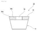
Fig. 16 , in a state where asensor chip 10 is mounted on asensor chip holder 56 fixed in an SPFS measurement device, the sensor chip is urged in the A direction. Then, areference surface 54a of the positioning and fixingpart 54 is brought into contact with the internal surface of thesensor chip holder 56, and thereby, positioning thereof in the A direction is done. - Further, the sensor chip is urged in the B direction, and then, a
reference surface 54b of the positioning and fixingpart 54 is brought into contact with the internal surface of thesensor chip holder 56, and thereby, positioning thereof in the B direction is done. - Although positioning and fixing parts in a convex shape have been formed as a positioning and fixing
part 54 in this example, the shape, number, setting position and the like of the positioning and fixingpart 54 can be appropriately changed depending on the shape of thesensor chip holder 56 on the side of the SPFS measurement device, for example, and a concave shape, a slit shape, or the like can be used. - By arranging like this, using the positioning and fixing
parts 54 molded integrally with thedielectric member 12, accurate positioning of thesensor chip 10 for SPFS measurement can be carried out in an SPFS measurement device with which detection is carried out; therefore, accurate adjustment between the position of the center of theligand immobilization part 38, which is a reaction part, and the position of the irradiated region can be carried out; and a highly precise and accurate SPFS measurement can be carried out. - Preferred embodiments of the present invention have been described above, but the present invention is not limited thereto. For example, although, in the above examples, the shape of the
dielectric member 12 constituting a prism is a hexahedron having a cross section of a substantially trapezoidal shape (a shape of a truncated quadrangular pyramid), the shape of thedielectric member 12 is not particularly limited, and may be changed to a shape of a triangular prism having a cross section of a triangle, for example. Like this, various modifications can be made within a scope not departing from the object of the present invention. - The present invention can be applied to a sensor chip for SPFS measurement that is used for a surface plasmon-field enhanced fluorescence spectrometry device using a surface plasmon-field enhanced fluorescence spectroscopy (SPFS; Surface Plasmon-field enhanced Fluorescence Spectroscopy) (hereinafter referred to simply as "SPFS") in the field of medical care or biotechnology, for example, and an SPFS measurement method using the sensor chip for SPFS measurement, and an SPFS measurement device equipped with the sensor chip for SPFS measurement.
-
- 10
- Sensor Chip for SPFS Measurement
- 12
- Dielectric Member
- 12a
- Side End Surface Position
- 14
- Metal Thin Film-Formed Surface
- 16
- Metal Thin Film
- 18
- Excitation Light Incoming Surface
- 20
- Reflected Light Outgoing Surface
- 22
- Side End Surface
- 23
- Side End Surface
- 24
- Resin Inlet
- 26
- Light Source
- 28
- Wavelength Separation Filter
- 30
- Deflecting Plate
- 32
- Light Collecting Means
- 34
- Wavelength Separation Filter
- 36
- Light Receiving Sensor
- 38
- Ligand Immobilization Part
- 40
- Bottom Part
- 42
- Channel Wall
- 44
- Channel Lid Member
- 46
- Channel
- 48
- Reagent Inlet
- 50
- Projected Part
- 52
- Both Side End Parts
- 54
- Positioning and Fixing Part
- 54a
- Reference Surface
- 56
- Sensor Chip Holder
Claims (13)
- A sensor chip for SPFS measurement which has a dielectric member constituting a prism, said dielectric member having been produced by carrying out injection molding of a resin, characterized in that said sensor chip for SPFS measurement has been arranged such that
a resin inlet is set on one side end surface of the dielectric member, said one side end surface intersecting with an excitation light incoming surface of said dielectric member, a metal thin film-formed surface of said dielectric member, and a reflected light outgoing surface through which a reflected light that comes in through said excitation light incoming surface and is reflected by the metal thin film-formed surface of said dielectric member goes out; and,
when viewing from the metal thin film-formed surface side of said dielectric member and taking as b the distance of the side end surface position of said resin inlet to the position on said metal thin film-formed surface that is farthest from the side end surface position of said resin inlet,
the center of a ligand immobilization part, which is a reaction part, is located in the area between the 3b/8 position and the 6b/8 position from the side end surface position of said resin inlet. - The sensor chip for SPFS measurement according to claim 1, characterized in that, on the metal thin film-formed surface of said dielectric member, a channel into which a specimen can be introduced has been formed.
- The sensor chip for SPFS measurement according to claim 2, characterized by having been arranged such that,
in said channel, said ligand immobilization part has been formed, and
the direction of the flow in said channel is parallel to the directions of said excitation light incoming surface and said reflected light outgoing surface of said dielectric member. - The sensor chip for SPFS measurement according to any one of claims 1 to 3, characterized in that, on said sensor chip for SPFS measurement, positioning and fixing parts to carry out positioning and fixing of the sensor chip for SPFS measurement in an SPFS measurement device with which detection is carried out are provided.
- The sensor chip for SPFS measurement according to claim 4, characterized in that said positioning and fixing parts have been formed in a channel lid member equipped on said dielectric member.
- The sensor chip for SPFS measurement according to claim 4, characterized in that said positioning and fixing parts have been formed in said dielectric member.
- An SPFS measurement method, characterized in that
a sensor chip for SPFS measurement which has a dielectric member constituting a prism, said dielectric member having been produced by carrying out injection molding of a resin,
wherein a resin inlet is set on one side end surface of the dielectric member, said one side end surface intersecting with an excitation light incoming surface of said dielectric member, a metal thin film-formed surface of said dielectric member, and a reflected light outgoing surface through which a reflected light that comes in through said excitation light incoming surface and is reflected by the metal thin film-formed surface of said dielectric member goes out,
is used;
when viewing from the metal thin film-formed surface side of said dielectric member and taking as b the distance of the side end surface position of said resin inlet to the position on said metal thin film-formed surface that is farthest from the side end surface position of said resin inlet,
an excitation light is irradiated to at least a portion of a metal thin film from the side where said dielectric member exists, said metal thin film having been formed on said dielectric member, said portion being located in the area between the 3b/8 position and the 6b/8 position from the side end surface position of said resin inlet; and
fluorescence that is emitted by a fluorescent substance labeling an analyte immobilized by a ligand on said metal thin film is measured to calculate the amount of the analyte. - The SPFS measurement method according to claim 7, characterized in that, on the metal thin film-formed surface of said dielectric member, a channel into which a specimen can be introduced has been formed.
- The SPFS measurement method according to claim 8, characterized by having been arranged such that,
in said channel, said ligand immobilization part has been formed, and
the direction of the flow in said channel is parallel to the directions of said excitation light incoming surface and said reflected light outgoing surface of said dielectric member. - The SPFS measurement method according to any one of claims 7 to 9, characterized in that, on said sensor chip for SPFS measurement, positioning and fixing parts to carry out positioning and fixing of the sensor chip for SPFS measurement in an SPFS measurement device with which detection is carried out are provided.
- The sensor chip for SPFS measurement according to claim 10, characterized in that said positioning and fixing parts have been formed in a channel lid member equipped on said dielectric member.
- The sensor chip for SPFS measurement according to claim 10, characterized in that said positioning and fixing parts have been formed in said dielectric member.
- An SPFS measurement device, characterized by being equipped with the sensor chip for SPFS measurement according to any one of claims 1 to 6.
Applications Claiming Priority (2)
| Application Number | Priority Date | Filing Date | Title |
|---|---|---|---|
| JP2011283962 | 2011-12-26 | ||
| PCT/JP2012/083483 WO2013099871A1 (en) | 2011-12-26 | 2012-12-25 | Spfs measurement sensor chip, spfs measurement method employing spfs measurement sensor chip, and spfs measurement device comprising spfs measurement sensor chip |
Publications (3)
| Publication Number | Publication Date |
|---|---|
| EP2799843A1 true EP2799843A1 (en) | 2014-11-05 |
| EP2799843A4 EP2799843A4 (en) | 2015-08-19 |
| EP2799843B1 EP2799843B1 (en) | 2019-08-21 |
Family
ID=48697356
Family Applications (1)
| Application Number | Title | Priority Date | Filing Date |
|---|---|---|---|
| EP12862962.3A Active EP2799843B1 (en) | 2011-12-26 | 2012-12-25 | Spfs measurement method employing spfs measurement sensor chip, and spfs measurement device comprising spfs measurement sensor chip |
Country Status (4)
| Country | Link |
|---|---|
| US (1) | US9970875B2 (en) |
| EP (1) | EP2799843B1 (en) |
| JP (1) | JP6098523B2 (en) |
| WO (1) | WO2013099871A1 (en) |
Families Citing this family (5)
| Publication number | Priority date | Publication date | Assignee | Title |
|---|---|---|---|---|
| EP2711689B1 (en) * | 2011-05-19 | 2020-01-01 | Konica Minolta, Inc. | Surface plasmon-field enhanced fluorescence measurement device and fluorescence detection method using same |
| EP3153845B1 (en) * | 2014-05-29 | 2020-05-27 | Konica Minolta, Inc. | Surface-plasmon enhanced fluorescence measurement method and surface-plasmon enhanced fluorescence measurement device |
| JP6638721B2 (en) * | 2015-02-20 | 2020-01-29 | コニカミノルタ株式会社 | Detection method and reaction device |
| EP3376208A4 (en) * | 2015-11-11 | 2019-02-20 | Konica Minolta, Inc. | OPTICAL SAMPLE DETECTION SYSTEM |
| CN117295938A (en) * | 2021-03-10 | 2023-12-26 | 尼科亚生命科学股份有限公司 | Surface plasmon resonance signal amplification |
Family Cites Families (10)
| Publication number | Priority date | Publication date | Assignee | Title |
|---|---|---|---|---|
| JP2002048904A (en) * | 2000-08-03 | 2002-02-15 | Canon Inc | Resin molded prism and its mold |
| JP4689907B2 (en) | 2001-09-28 | 2011-06-01 | 富士フイルム株式会社 | Measuring chip and manufacturing method thereof |
| US20020127706A1 (en) * | 2001-01-25 | 2002-09-12 | Fuji Photo Film Co., Ltd. | Surface plasmon resonance measuring chip and method of manufacture thereof |
| JP2006208294A (en) | 2005-01-31 | 2006-08-10 | Canon Inc | Simultaneous plasmon resonance and fluorescence imaging apparatus and imaging method |
| JP2007248430A (en) * | 2006-03-20 | 2007-09-27 | Fujifilm Corp | Sensor unit and total reflection prism |
| JP4664221B2 (en) | 2006-03-20 | 2011-04-06 | 富士フイルム株式会社 | Sensor unit and total reflection prism |
| JP2010127624A (en) | 2008-11-25 | 2010-06-10 | Fujifilm Corp | Total reflection illuminated sensor chip |
| JP5285471B2 (en) * | 2009-03-11 | 2013-09-11 | 富士フイルム株式会社 | Total reflection illumination type sensor chip, manufacturing method thereof, and sensing method using the same |
| JP5831230B2 (en) | 2009-12-14 | 2015-12-09 | コニカミノルタ株式会社 | Surface plasmon enhanced fluorescence measurement device |
| JP5663905B2 (en) * | 2010-03-08 | 2015-02-04 | コニカミノルタ株式会社 | Chip structure |
-
2012
- 2012-12-25 EP EP12862962.3A patent/EP2799843B1/en active Active
- 2012-12-25 US US14/367,323 patent/US9970875B2/en active Active
- 2012-12-25 WO PCT/JP2012/083483 patent/WO2013099871A1/en not_active Ceased
- 2012-12-25 JP JP2013551705A patent/JP6098523B2/en active Active
Also Published As
| Publication number | Publication date |
|---|---|
| US9970875B2 (en) | 2018-05-15 |
| WO2013099871A1 (en) | 2013-07-04 |
| JP6098523B2 (en) | 2017-03-22 |
| US20150011015A1 (en) | 2015-01-08 |
| JPWO2013099871A1 (en) | 2015-05-07 |
| EP2799843A4 (en) | 2015-08-19 |
| EP2799843B1 (en) | 2019-08-21 |
Similar Documents
| Publication | Publication Date | Title |
|---|---|---|
| JP5573843B2 (en) | Surface plasmon enhanced fluorescence measurement device | |
| US20090069199A1 (en) | Method and device for optical detection of substances in a liquid or gaseous medium | |
| EP2799843B1 (en) | Spfs measurement method employing spfs measurement sensor chip, and spfs measurement device comprising spfs measurement sensor chip | |
| EP2711689B1 (en) | Surface plasmon-field enhanced fluorescence measurement device and fluorescence detection method using same | |
| WO2012051206A1 (en) | System and method for cell analysis | |
| US20080245971A1 (en) | Biosensors with Improved Sensitivity | |
| JPWO2015129361A1 (en) | Sensor chip for surface plasmon excitation enhanced fluorescence spectroscopy | |
| EP2962086B1 (en) | Sample plate and analyzing method | |
| EP2189782A2 (en) | Total reflection illuminated sensor chip | |
| JP5516198B2 (en) | Plasmon excitation sensor chip, plasmon excitation sensor using the same, and analyte detection method | |
| JP2011257216A (en) | Surface plasmon enhanced fluorescence sensor, and chip structure unit used for surface plasmon enhanced fluorescence sensor | |
| EP3683571A1 (en) | Diffracted light removal slit and optical sample detection system using same | |
| JP5663905B2 (en) | Chip structure | |
| CN104105956B (en) | Microstructured chip for surface plasmon resonance analysis, analysis device comprising said microstructured chip and use of said device | |
| JP5655917B2 (en) | Chip structure | |
| JPWO2019221040A1 (en) | Specimen detection chip and sample detection device using it | |
| JP5831177B2 (en) | Measuring method and measuring device | |
| WO2014007134A1 (en) | Sensor chip | |
| WO2011074373A1 (en) | Surface plasmon enhanced fluorescence measurement device and chip structure | |
| JP6885458B2 (en) | Sensor chip for sample detection system | |
| JP6205993B2 (en) | Analysis chip | |
| WO2014178385A1 (en) | Target substance-capturing device and target substance detection device | |
| JP6638343B2 (en) | Sensor chip and optical sample detection system equipped with the sensor chip | |
| JPWO2014021171A1 (en) | Method for manufacturing sensor member, method for manufacturing sensor chip, and method for using sensor member | |
| JP5786985B2 (en) | Surface plasmon enhanced fluorescence sensor and chip structure unit used for surface plasmon enhanced fluorescence sensor |
Legal Events
| Date | Code | Title | Description |
|---|---|---|---|
| PUAI | Public reference made under article 153(3) epc to a published international application that has entered the european phase |
Free format text: ORIGINAL CODE: 0009012 |
|
| 17P | Request for examination filed |
Effective date: 20140627 |
|
| AK | Designated contracting states |
Kind code of ref document: A1 Designated state(s): AL AT BE BG CH CY CZ DE DK EE ES FI FR GB GR HR HU IE IS IT LI LT LU LV MC MK MT NL NO PL PT RO RS SE SI SK SM TR |
|
| DAX | Request for extension of the european patent (deleted) | ||
| RIN1 | Information on inventor provided before grant (corrected) |
Inventor name: MATSUO, MASATAKA Inventor name: ISHIDA, KENJI |
|
| RA4 | Supplementary search report drawn up and despatched (corrected) |
Effective date: 20150722 |
|
| RIC1 | Information provided on ipc code assigned before grant |
Ipc: G01N 21/64 20060101AFI20150716BHEP |
|
| STAA | Information on the status of an ep patent application or granted ep patent |
Free format text: STATUS: EXAMINATION IS IN PROGRESS |
|
| 17Q | First examination report despatched |
Effective date: 20170807 |
|
| GRAP | Despatch of communication of intention to grant a patent |
Free format text: ORIGINAL CODE: EPIDOSNIGR1 |
|
| STAA | Information on the status of an ep patent application or granted ep patent |
Free format text: STATUS: GRANT OF PATENT IS INTENDED |
|
| INTG | Intention to grant announced |
Effective date: 20190402 |
|
| GRAS | Grant fee paid |
Free format text: ORIGINAL CODE: EPIDOSNIGR3 |
|
| GRAA | (expected) grant |
Free format text: ORIGINAL CODE: 0009210 |
|
| STAA | Information on the status of an ep patent application or granted ep patent |
Free format text: STATUS: THE PATENT HAS BEEN GRANTED |
|
| AK | Designated contracting states |
Kind code of ref document: B1 Designated state(s): AL AT BE BG CH CY CZ DE DK EE ES FI FR GB GR HR HU IE IS IT LI LT LU LV MC MK MT NL NO PL PT RO RS SE SI SK SM TR |
|
| REG | Reference to a national code |
Ref country code: GB Ref legal event code: FG4D |
|
| REG | Reference to a national code |
Ref country code: CH Ref legal event code: EP |
|
| REG | Reference to a national code |
Ref country code: DE Ref legal event code: R096 Ref document number: 602012063251 Country of ref document: DE |
|
| REG | Reference to a national code |
Ref country code: AT Ref legal event code: REF Ref document number: 1170305 Country of ref document: AT Kind code of ref document: T Effective date: 20190915 |
|
| REG | Reference to a national code |
Ref country code: IE Ref legal event code: FG4D |
|
| REG | Reference to a national code |
Ref country code: LT Ref legal event code: MG4D |
|
| REG | Reference to a national code |
Ref country code: NL Ref legal event code: MP Effective date: 20190821 |
|
| PG25 | Lapsed in a contracting state [announced via postgrant information from national office to epo] |
Ref country code: BG Free format text: LAPSE BECAUSE OF FAILURE TO SUBMIT A TRANSLATION OF THE DESCRIPTION OR TO PAY THE FEE WITHIN THE PRESCRIBED TIME-LIMIT Effective date: 20191121 Ref country code: SE Free format text: LAPSE BECAUSE OF FAILURE TO SUBMIT A TRANSLATION OF THE DESCRIPTION OR TO PAY THE FEE WITHIN THE PRESCRIBED TIME-LIMIT Effective date: 20190821 Ref country code: NO Free format text: LAPSE BECAUSE OF FAILURE TO SUBMIT A TRANSLATION OF THE DESCRIPTION OR TO PAY THE FEE WITHIN THE PRESCRIBED TIME-LIMIT Effective date: 20191121 Ref country code: NL Free format text: LAPSE BECAUSE OF FAILURE TO SUBMIT A TRANSLATION OF THE DESCRIPTION OR TO PAY THE FEE WITHIN THE PRESCRIBED TIME-LIMIT Effective date: 20190821 Ref country code: LT Free format text: LAPSE BECAUSE OF FAILURE TO SUBMIT A TRANSLATION OF THE DESCRIPTION OR TO PAY THE FEE WITHIN THE PRESCRIBED TIME-LIMIT Effective date: 20190821 Ref country code: FI Free format text: LAPSE BECAUSE OF FAILURE TO SUBMIT A TRANSLATION OF THE DESCRIPTION OR TO PAY THE FEE WITHIN THE PRESCRIBED TIME-LIMIT Effective date: 20190821 Ref country code: HR Free format text: LAPSE BECAUSE OF FAILURE TO SUBMIT A TRANSLATION OF THE DESCRIPTION OR TO PAY THE FEE WITHIN THE PRESCRIBED TIME-LIMIT Effective date: 20190821 Ref country code: PT Free format text: LAPSE BECAUSE OF FAILURE TO SUBMIT A TRANSLATION OF THE DESCRIPTION OR TO PAY THE FEE WITHIN THE PRESCRIBED TIME-LIMIT Effective date: 20191223 |
|
| PG25 | Lapsed in a contracting state [announced via postgrant information from national office to epo] |
Ref country code: GR Free format text: LAPSE BECAUSE OF FAILURE TO SUBMIT A TRANSLATION OF THE DESCRIPTION OR TO PAY THE FEE WITHIN THE PRESCRIBED TIME-LIMIT Effective date: 20191122 Ref country code: ES Free format text: LAPSE BECAUSE OF FAILURE TO SUBMIT A TRANSLATION OF THE DESCRIPTION OR TO PAY THE FEE WITHIN THE PRESCRIBED TIME-LIMIT Effective date: 20190821 Ref country code: LV Free format text: LAPSE BECAUSE OF FAILURE TO SUBMIT A TRANSLATION OF THE DESCRIPTION OR TO PAY THE FEE WITHIN THE PRESCRIBED TIME-LIMIT Effective date: 20190821 Ref country code: AL Free format text: LAPSE BECAUSE OF FAILURE TO SUBMIT A TRANSLATION OF THE DESCRIPTION OR TO PAY THE FEE WITHIN THE PRESCRIBED TIME-LIMIT Effective date: 20190821 Ref country code: RS Free format text: LAPSE BECAUSE OF FAILURE TO SUBMIT A TRANSLATION OF THE DESCRIPTION OR TO PAY THE FEE WITHIN THE PRESCRIBED TIME-LIMIT Effective date: 20190821 Ref country code: IS Free format text: LAPSE BECAUSE OF FAILURE TO SUBMIT A TRANSLATION OF THE DESCRIPTION OR TO PAY THE FEE WITHIN THE PRESCRIBED TIME-LIMIT Effective date: 20191221 |
|
| REG | Reference to a national code |
Ref country code: AT Ref legal event code: MK05 Ref document number: 1170305 Country of ref document: AT Kind code of ref document: T Effective date: 20190821 |
|
| PG25 | Lapsed in a contracting state [announced via postgrant information from national office to epo] |
Ref country code: TR Free format text: LAPSE BECAUSE OF FAILURE TO SUBMIT A TRANSLATION OF THE DESCRIPTION OR TO PAY THE FEE WITHIN THE PRESCRIBED TIME-LIMIT Effective date: 20190821 |
|
| PG25 | Lapsed in a contracting state [announced via postgrant information from national office to epo] |
Ref country code: AT Free format text: LAPSE BECAUSE OF FAILURE TO SUBMIT A TRANSLATION OF THE DESCRIPTION OR TO PAY THE FEE WITHIN THE PRESCRIBED TIME-LIMIT Effective date: 20190821 Ref country code: DK Free format text: LAPSE BECAUSE OF FAILURE TO SUBMIT A TRANSLATION OF THE DESCRIPTION OR TO PAY THE FEE WITHIN THE PRESCRIBED TIME-LIMIT Effective date: 20190821 Ref country code: IT Free format text: LAPSE BECAUSE OF FAILURE TO SUBMIT A TRANSLATION OF THE DESCRIPTION OR TO PAY THE FEE WITHIN THE PRESCRIBED TIME-LIMIT Effective date: 20190821 Ref country code: EE Free format text: LAPSE BECAUSE OF FAILURE TO SUBMIT A TRANSLATION OF THE DESCRIPTION OR TO PAY THE FEE WITHIN THE PRESCRIBED TIME-LIMIT Effective date: 20190821 Ref country code: PL Free format text: LAPSE BECAUSE OF FAILURE TO SUBMIT A TRANSLATION OF THE DESCRIPTION OR TO PAY THE FEE WITHIN THE PRESCRIBED TIME-LIMIT Effective date: 20190821 Ref country code: RO Free format text: LAPSE BECAUSE OF FAILURE TO SUBMIT A TRANSLATION OF THE DESCRIPTION OR TO PAY THE FEE WITHIN THE PRESCRIBED TIME-LIMIT Effective date: 20190821 |
|
| PG25 | Lapsed in a contracting state [announced via postgrant information from national office to epo] |
Ref country code: IS Free format text: LAPSE BECAUSE OF FAILURE TO SUBMIT A TRANSLATION OF THE DESCRIPTION OR TO PAY THE FEE WITHIN THE PRESCRIBED TIME-LIMIT Effective date: 20200224 Ref country code: CZ Free format text: LAPSE BECAUSE OF FAILURE TO SUBMIT A TRANSLATION OF THE DESCRIPTION OR TO PAY THE FEE WITHIN THE PRESCRIBED TIME-LIMIT Effective date: 20190821 Ref country code: SK Free format text: LAPSE BECAUSE OF FAILURE TO SUBMIT A TRANSLATION OF THE DESCRIPTION OR TO PAY THE FEE WITHIN THE PRESCRIBED TIME-LIMIT Effective date: 20190821 Ref country code: SM Free format text: LAPSE BECAUSE OF FAILURE TO SUBMIT A TRANSLATION OF THE DESCRIPTION OR TO PAY THE FEE WITHIN THE PRESCRIBED TIME-LIMIT Effective date: 20190821 |
|
| REG | Reference to a national code |
Ref country code: DE Ref legal event code: R097 Ref document number: 602012063251 Country of ref document: DE |
|
| PLBE | No opposition filed within time limit |
Free format text: ORIGINAL CODE: 0009261 |
|
| STAA | Information on the status of an ep patent application or granted ep patent |
Free format text: STATUS: NO OPPOSITION FILED WITHIN TIME LIMIT |
|
| PG2D | Information on lapse in contracting state deleted |
Ref country code: IS |
|
| REG | Reference to a national code |
Ref country code: CH Ref legal event code: PL |
|
| 26N | No opposition filed |
Effective date: 20200603 |
|
| REG | Reference to a national code |
Ref country code: BE Ref legal event code: MM Effective date: 20191231 |
|
| PG25 | Lapsed in a contracting state [announced via postgrant information from national office to epo] |
Ref country code: SI Free format text: LAPSE BECAUSE OF FAILURE TO SUBMIT A TRANSLATION OF THE DESCRIPTION OR TO PAY THE FEE WITHIN THE PRESCRIBED TIME-LIMIT Effective date: 20190821 Ref country code: MC Free format text: LAPSE BECAUSE OF FAILURE TO SUBMIT A TRANSLATION OF THE DESCRIPTION OR TO PAY THE FEE WITHIN THE PRESCRIBED TIME-LIMIT Effective date: 20190821 |
|
| PG25 | Lapsed in a contracting state [announced via postgrant information from national office to epo] |
Ref country code: IE Free format text: LAPSE BECAUSE OF NON-PAYMENT OF DUE FEES Effective date: 20191225 Ref country code: LU Free format text: LAPSE BECAUSE OF NON-PAYMENT OF DUE FEES Effective date: 20191225 |
|
| PG25 | Lapsed in a contracting state [announced via postgrant information from national office to epo] |
Ref country code: CH Free format text: LAPSE BECAUSE OF NON-PAYMENT OF DUE FEES Effective date: 20191231 Ref country code: BE Free format text: LAPSE BECAUSE OF NON-PAYMENT OF DUE FEES Effective date: 20191231 Ref country code: LI Free format text: LAPSE BECAUSE OF NON-PAYMENT OF DUE FEES Effective date: 20191231 |
|
| PG25 | Lapsed in a contracting state [announced via postgrant information from national office to epo] |
Ref country code: CY Free format text: LAPSE BECAUSE OF FAILURE TO SUBMIT A TRANSLATION OF THE DESCRIPTION OR TO PAY THE FEE WITHIN THE PRESCRIBED TIME-LIMIT Effective date: 20190821 |
|
| PG25 | Lapsed in a contracting state [announced via postgrant information from national office to epo] |
Ref country code: HU Free format text: LAPSE BECAUSE OF FAILURE TO SUBMIT A TRANSLATION OF THE DESCRIPTION OR TO PAY THE FEE WITHIN THE PRESCRIBED TIME-LIMIT; INVALID AB INITIO Effective date: 20121225 Ref country code: MT Free format text: LAPSE BECAUSE OF FAILURE TO SUBMIT A TRANSLATION OF THE DESCRIPTION OR TO PAY THE FEE WITHIN THE PRESCRIBED TIME-LIMIT Effective date: 20190821 |
|
| REG | Reference to a national code |
Ref country code: DE Ref legal event code: R081 Ref document number: 602012063251 Country of ref document: DE Owner name: OTSUKA PHARMACEUTICAL CO., LTD., JP Free format text: FORMER OWNER: KONICA MINOLTA, INC., TOKYO, JP |
|
| REG | Reference to a national code |
Ref country code: GB Ref legal event code: 732E Free format text: REGISTERED BETWEEN 20220428 AND 20220504 |
|
| PG25 | Lapsed in a contracting state [announced via postgrant information from national office to epo] |
Ref country code: MK Free format text: LAPSE BECAUSE OF FAILURE TO SUBMIT A TRANSLATION OF THE DESCRIPTION OR TO PAY THE FEE WITHIN THE PRESCRIBED TIME-LIMIT Effective date: 20190821 |
|
| P01 | Opt-out of the competence of the unified patent court (upc) registered |
Effective date: 20230512 |
|
| PGFP | Annual fee paid to national office [announced via postgrant information from national office to epo] |
Ref country code: DE Payment date: 20251126 Year of fee payment: 14 |
|
| PGFP | Annual fee paid to national office [announced via postgrant information from national office to epo] |
Ref country code: GB Payment date: 20251119 Year of fee payment: 14 |
|
| PGFP | Annual fee paid to national office [announced via postgrant information from national office to epo] |
Ref country code: FR Payment date: 20251120 Year of fee payment: 14 |