EP2797129A1 - Semiconductor light emitting apparatus - Google Patents
Semiconductor light emitting apparatus Download PDFInfo
- Publication number
- EP2797129A1 EP2797129A1 EP20140020055 EP14020055A EP2797129A1 EP 2797129 A1 EP2797129 A1 EP 2797129A1 EP 20140020055 EP20140020055 EP 20140020055 EP 14020055 A EP14020055 A EP 14020055A EP 2797129 A1 EP2797129 A1 EP 2797129A1
- Authority
- EP
- European Patent Office
- Prior art keywords
- layer
- electrode
- light emitting
- semiconductor
- semiconductor layer
- Prior art date
- Legal status (The legal status is an assumption and is not a legal conclusion. Google has not performed a legal analysis and makes no representation as to the accuracy of the status listed.)
- Granted
Links
Images
















Classifications
-
- H—ELECTRICITY
- H10—SEMICONDUCTOR DEVICES; ELECTRIC SOLID-STATE DEVICES NOT OTHERWISE PROVIDED FOR
- H10H—INORGANIC LIGHT-EMITTING SEMICONDUCTOR DEVICES HAVING POTENTIAL BARRIERS
- H10H20/00—Individual inorganic light-emitting semiconductor devices having potential barriers, e.g. light-emitting diodes [LED]
- H10H20/80—Constructional details
- H10H20/83—Electrodes
- H10H20/832—Electrodes characterised by their material
- H10H20/835—Reflective materials
-
- H—ELECTRICITY
- H10—SEMICONDUCTOR DEVICES; ELECTRIC SOLID-STATE DEVICES NOT OTHERWISE PROVIDED FOR
- H10H—INORGANIC LIGHT-EMITTING SEMICONDUCTOR DEVICES HAVING POTENTIAL BARRIERS
- H10H20/00—Individual inorganic light-emitting semiconductor devices having potential barriers, e.g. light-emitting diodes [LED]
- H10H20/80—Constructional details
- H10H20/81—Bodies
- H10H20/811—Bodies having quantum effect structures or superlattices, e.g. tunnel junctions
- H10H20/812—Bodies having quantum effect structures or superlattices, e.g. tunnel junctions within the light-emitting regions, e.g. having quantum confinement structures
-
- H—ELECTRICITY
- H10—SEMICONDUCTOR DEVICES; ELECTRIC SOLID-STATE DEVICES NOT OTHERWISE PROVIDED FOR
- H10H—INORGANIC LIGHT-EMITTING SEMICONDUCTOR DEVICES HAVING POTENTIAL BARRIERS
- H10H20/00—Individual inorganic light-emitting semiconductor devices having potential barriers, e.g. light-emitting diodes [LED]
- H10H20/80—Constructional details
- H10H20/81—Bodies
- H10H20/813—Bodies having a plurality of light-emitting regions, e.g. multi-junction LEDs or light-emitting devices having photoluminescent regions within the bodies
-
- H—ELECTRICITY
- H10—SEMICONDUCTOR DEVICES; ELECTRIC SOLID-STATE DEVICES NOT OTHERWISE PROVIDED FOR
- H10H—INORGANIC LIGHT-EMITTING SEMICONDUCTOR DEVICES HAVING POTENTIAL BARRIERS
- H10H20/00—Individual inorganic light-emitting semiconductor devices having potential barriers, e.g. light-emitting diodes [LED]
- H10H20/80—Constructional details
- H10H20/83—Electrodes
- H10H20/831—Electrodes characterised by their shape
- H10H20/8312—Electrodes characterised by their shape extending at least partially through the bodies
-
- H—ELECTRICITY
- H10—SEMICONDUCTOR DEVICES; ELECTRIC SOLID-STATE DEVICES NOT OTHERWISE PROVIDED FOR
- H10H—INORGANIC LIGHT-EMITTING SEMICONDUCTOR DEVICES HAVING POTENTIAL BARRIERS
- H10H20/00—Individual inorganic light-emitting semiconductor devices having potential barriers, e.g. light-emitting diodes [LED]
- H10H20/01—Manufacture or treatment
- H10H20/011—Manufacture or treatment of bodies, e.g. forming semiconductor layers
- H10H20/018—Bonding of wafers
-
- H—ELECTRICITY
- H10—SEMICONDUCTOR DEVICES; ELECTRIC SOLID-STATE DEVICES NOT OTHERWISE PROVIDED FOR
- H10H—INORGANIC LIGHT-EMITTING SEMICONDUCTOR DEVICES HAVING POTENTIAL BARRIERS
- H10H20/00—Individual inorganic light-emitting semiconductor devices having potential barriers, e.g. light-emitting diodes [LED]
- H10H20/80—Constructional details
- H10H20/85—Packages
- H10H20/855—Optical field-shaping means, e.g. lenses
- H10H20/856—Reflecting means
-
- H—ELECTRICITY
- H10—SEMICONDUCTOR DEVICES; ELECTRIC SOLID-STATE DEVICES NOT OTHERWISE PROVIDED FOR
- H10H—INORGANIC LIGHT-EMITTING SEMICONDUCTOR DEVICES HAVING POTENTIAL BARRIERS
- H10H20/00—Individual inorganic light-emitting semiconductor devices having potential barriers, e.g. light-emitting diodes [LED]
- H10H20/80—Constructional details
- H10H20/85—Packages
- H10H20/857—Interconnections, e.g. lead-frames, bond wires or solder balls
-
- H—ELECTRICITY
- H10—SEMICONDUCTOR DEVICES; ELECTRIC SOLID-STATE DEVICES NOT OTHERWISE PROVIDED FOR
- H10W—GENERIC PACKAGES, INTERCONNECTIONS, CONNECTORS OR OTHER CONSTRUCTIONAL DETAILS OF DEVICES COVERED BY CLASS H10
- H10W72/00—Interconnections or connectors in packages
- H10W72/50—Bond wires
- H10W72/531—Shapes of wire connectors
- H10W72/536—Shapes of wire connectors the connected ends being ball-shaped
-
- H—ELECTRICITY
- H10—SEMICONDUCTOR DEVICES; ELECTRIC SOLID-STATE DEVICES NOT OTHERWISE PROVIDED FOR
- H10W—GENERIC PACKAGES, INTERCONNECTIONS, CONNECTORS OR OTHER CONSTRUCTIONAL DETAILS OF DEVICES COVERED BY CLASS H10
- H10W72/00—Interconnections or connectors in packages
- H10W72/50—Bond wires
- H10W72/551—Materials of bond wires
- H10W72/552—Materials of bond wires comprising metals or metalloids, e.g. silver
- H10W72/5522—Materials of bond wires comprising metals or metalloids, e.g. silver comprising gold [Au]
-
- H—ELECTRICITY
- H10—SEMICONDUCTOR DEVICES; ELECTRIC SOLID-STATE DEVICES NOT OTHERWISE PROVIDED FOR
- H10W—GENERIC PACKAGES, INTERCONNECTIONS, CONNECTORS OR OTHER CONSTRUCTIONAL DETAILS OF DEVICES COVERED BY CLASS H10
- H10W90/00—Package configurations
- H10W90/701—Package configurations characterised by the relative positions of pads or connectors relative to package parts
- H10W90/721—Package configurations characterised by the relative positions of pads or connectors relative to package parts of bump connectors
- H10W90/722—Package configurations characterised by the relative positions of pads or connectors relative to package parts of bump connectors between stacked chips
Definitions
- the present invention relates to a semiconductor light emitting apparatus.
- the semiconductor light emitting apparatus has a semiconductor lamination including an n-type semiconductor layer and a p-type semiconductor layer, an n-side electrode electrically connected to the n-type semiconductor layer, and a p-side electrode electrically connected to the p-type semiconductor layer.
- a semiconductor lamination including an n-type semiconductor layer and a p-type semiconductor layer, an n-side electrode electrically connected to the n-type semiconductor layer, and a p-side electrode electrically connected to the p-type semiconductor layer.
- a p-side electrode is formed on the p-type semiconductor layer
- a recess exposing the n-type semiconductor layer is formed from the side of the p-type semiconductor layer
- an n-side electrode is formed on the recess
- the n-side electrode and the p-side electrode can be disposed on the same side of the semiconductor lamination (for example, see Japanese Laid-open Patent Publication No.
- An object of the embodiment is to provide a semiconductor light emitting apparatus having a novel electrode structure.
- a semiconductor light emitting apparatus comprising:
- the light extracting efficiency can be enhanced by forming the light reflective electrode layer of the first electrode overlapping the second electrode at the peripheral portion.
- Figs. 1A to 1L are schematic cross-sectional views illustrating processes of manufacturing a semiconductor light emitting element according to the first embodiment.
- a nitride-series semiconductor light emitting element is formed.
- the term "nitride series” means compound including nitrogen as group V element.
- MOCVD metal organic chemical vapor deposition
- a plurality of light emitting elements is formed at the same time on one growth substrate.
- Figs. 1A to 1L illustrate process of manufacturing representative one element.
- a sapphire substrate is prepared as a growth substrate 1.
- the growth substrate 1 is loaded in an MOCVD apparatus, and thermal cleaning is performed.
- a GaN buffer layer and an undoped GaN layer are grown on a cleaned substrate, and then an n-type GaN layer 2 doped with n-type impurity such as Si and having a film thickness of about 5 ⁇ m is grown.
- the GaN buffer layer and the undoped GaN layer are collectively illustrated as the n-type GaN layer 2.
- a light emitting layer (active layer) 3 is grown on the n-type GaN layer 2.
- a multiple quantum well structure including, for example, InGaN layers as well layers, and GaN layers as barrier layers alternately laminated, is formed as the light emitting layer 3.
- the growth substrate 1 is a single-crystal substrate having a lattice constant that enables epitaxial growth of GaN.
- a material is selected from those which are transparent to the light at a wavelength of 362 nm, absorption edge wavelength of GaN, so that the substrate can be peeled off by laser lift-off in a later process.
- Spinel, SiC, ZnO, and the like may be used, as well as sapphire.
- a reflective metal layer for example formed of Ag added with additive such as as Ni, Pt, Ti, or Pd and having a thickness of 200 nm is deposited by electron beam vapor deposition on the p-type GaN layer 4, and is patterned by lift-off to form a p-side electrode 5 of desired shape.
- the p-side electrode layer 5 includes one material selected from the group consisting of Ag, Pt, Ni, Al, Pd, and alloys thereof, so as to serve as a reflective electrode.
- Fig. 2 is a schematic plan view illustrating a plane structure of contact portions of p-side electrodes 51p and n-side electrodes 51n with semiconductor layers in the semiconductor light emitting element of embodiment.
- the p-side electrode 51p is formed spreading on the upper surface of the p-type semiconductor layer. Holes HL are formed to distribute discretely in the p-side electrode 51p, for example, in matrix shape. Inside each hole HL, an n-side electrode (via electrode) 51n is disposed.
- One element may have a rectangular shape having, for example, a size of about 600 ⁇ m x 1300 ⁇ m.
- the number of via electrodes 51n arranged in one element is, for example, about 40.
- Fig. 1B and other figures representatively illustrate processes of forming one n-side via electrode and illustrate one hole HL formed in the p-side electrode layer 5.
- a fringe layer 6 is formed by depositing an SiO 2 layer having a film thickness equal to the thickness of the p-side electrode layer 5, for example, by sputtering on the p-type GaN layer 4 outside the p-side electrode layer 5 so as to surround the circumference of the p-side electrode layer 5.
- an Ag layer of a thickness of 100 nm which will become a highly reflective layer is deposited for example by sputtering, and successively TiW/ Ti/ Pt/ Au/ Ti lamination (left side layer is formed on the substrate side or lower side, to represent laminated structure), which will become diffusion preventing layer, is formed with thicknesses 250 nm/ 50 nm/ 100 nm/ 1000 nm/ 30 nm for example by sputtering, and the lamination is patterned by lift-ofF, to form a p-side highly reflective cap layer 9.
- the p-side electrode layer 5 is doped with additive such as Ni, Pt, Ti, or Pd to enhance ohmic contact with the p-type GaN layer 4. In contrast, no additive is doped to the p-side highly reflective layer 7.
- the p-side diffusion preventing layer 8 serves to prevent diffusion of elements used in the p-side electrode layer 5 and the p-side highly reflective layer 7.
- the p-side diffusion preventive layer 8 can use Ti, W, Pt, Pd, Mo, Ru, Ir, Au, and an alloy thereof.
- the p-side highly reflective cap layer 9 is not formed in the vicinity of the edge of the hole HL, and the edge of the p-side highly reflective cap layer 9 on the side of the hole HL is disposed to be separated from the edge of the hole HL to the outer side.
- the peripheral portion of the p-side diffusion preventive layer 8 is formed to cover the peripheral portion of the p-side highly reflective cap layer 9. In plan view, the edge of the p-side diffusion preventive layer 8 is disposed inside the edge of the p-side highly reflective layer 7.
- the edge of the p-side highly reflective layer 7 coincides with the edge of the p-side diffusion preventive layer 8, and is disposed on the upper surface of the fringe layer 6.
- the structure in which the edge of the p-side highly reflective cap layer 9 is disposed on the upper surface of the fringe layer 6, i.e. separated from the semiconductor layers 2, 3, and 4 functions as a leakage stopper of Ag in the p-side highly reflective cap layer 9.
- an insulating cap layer 10 is formed by depositing an SiO 2 film having a thickness of 300 nm, covering the p-side highly reflective cap layer 9, the p-side electrode layer 5, and the fringe layer 6, for example by sputtering, and is patterned by lift-off.
- the patterning method dry etching using CF 4 -based gas, for example, can be used after forming a layer of SiO 2 on the entire surface, as well as the lift-off.
- the insulating cap layer 10 has a function of preventing leakage of the Ag-based material used in the p-side electrode layer 5 and the p-side highly reflective layer 7 of the p-side highly reflective cap layer 9.
- An insulating material such as SiO 2 , or SiN can also be used.
- the insulating cap layer 10 is formed to cover the edge of the hole HL and to extend on the side surface of the p-side electrode layer 5 that defines the hole HL.
- the side surfaces of the p-side electrode layer 5 are covered with the insulating cap layer 10.
- the insulating cap layer 10 has a corresponding opening OP in the hole HL, and the p-type GaN layer 4 is exposed at the bottom of the opening OP.
- the p-type GaN layer 4 exposed in the opening OP of the insulating cap layer 10 and the light emitting layer 3 therebelow are removed by, for example, reactive ion etching (RIE), to expose the n-type GaN layer, forming a recess CV which provides a contact area for an n-side electrode.
- RIE reactive ion etching
- an n-side via electrode 11 is formed on the n-type GaN layer 2 exposed at the bottom of the recess CV, using lift-off, using, for example Al, or preferably Ag or an Ag alloy from the viewpoint of high reflectance.
- a Ti film 11p having a thickness of 1 nm may be vapor deposited under the Ag or Ag alloy layer as a contact material with the n-type GaN layer 2 to provide appropriate contact resistance and high reflectance.
- the diameter of one hole HL formed in the p-side electrode layer 5 is about 40 ⁇ m
- the diameter of the edge of the recess CV is about 35 ⁇ m
- the diameter of the bottom portion of the via electrode 11 is about 30 ⁇ m.
- an insulating floating layer 12 is formed by depositing an SiO 2 film having a thickness of 600 nm by sputtering, covering the p-side electrode layer 5, the fringe layer 6, the p-side highly reflective cap layer 9, and the insulating cap layer 10, and patterning by lift-off or dry etching using CF 4 -based gas.
- An insulating material such as SiO 2 , or SiN can be used, as a material of the floating layer 12.
- the insulating floating layer 12 is formed to extend to the inside of the opening OP and the recess CV, covering the pn junction region exposed to the side surface of the recess CV.
- the insulating floating layer 12 has an opening on the upper surface of the n-side via electrode 11.
- An inter-electrode insulating layer IS between the p-side and the n-side electrodes is formed by the lamination of the insulating cap layer 10 and the insulating floating layer 12.
- the inter-electrode insulating layer IS is interposed between a p-side electrode Ep and an n-side electrode En to be completed by the later process, and electrically separates the p-side electrode Ep and the n-side electrode En.
- a contact hole CH for connecting the p-side electrode is formed by removing a partial region of the inter-electrode insulating layer IS, for example, in the vicinity of the edge portion of the element, for example, by RIE, and exposing the upper surface of the p-side highly reflective cap layer 9.
- an n-side highly reflective layer 13 is formed by depositing Ag/ Ti/ Pt/ Au layers respectively having thicknesses of 200 nm, 100 nm, 200 nm, and 200 nm on the n-side via electrode 11, for example, by electron beam deposition or sputtering, and by patterning using lift-off.
- a function of reflecting light progressing from the lower side through the insulating layers 10 and 12 and returning light to an n-type semiconductor layer 2 side is provided.
- a Ti layer 13p may be formed as an undercoat of the Ag layer in order to enhance the adhesion with the insulating layer 12. However, the reflectance is reduced by Ti, so the thickness of the Ti layer 13p is preferably selected 5 nm or less, for example, 1 nm.
- the n-side highly reflective layer 13 is formed so that the peripheral portion of the n-side highly reflective layer 13 overlaps the peripheral portion of the p-side electrode layer 5 which defines the hole HL. Details of the arrangement of the n-side highly reflective layer 13 with related elements will be described with reference to Fig. 3A .
- a conductive layer 14 divided in n-side portion and p-side portion is formed by depositing Ti/ Pt/ Au layers respectively having thicknesses of 50 nm, 100 nm, and 400 nm by electron beam deposition or sputtering, and performing patterning by lift-off.
- Portion of the conductive layer 14 which extends from above the n-side highly reflective layer 13 onto the inter-electrode insulating layer IS covering the p-side highly reflective cap layer 9 forms an n-side cap layer (n-side connection electrode) 14n.
- the n-side via electrode 11, the n-side highly reflective layer 13, and the n-side cap layer 14n form the n-side electrode En of the element.
- Portion of the conductive layer 14 which is formed in the contact hole CH and is electrically separated from the n-side cap layer 14n by interposing a gap from the n-side cap layer 14n forms a p-side connection electrode 14p.
- the p-side electrode layer 5, the p-side highly reflective cap layer 9, and the p-side connection electrode 14p form the p-side electrode Ep of the element.
- street ST is formed by removing the p-type semiconductor layer 4, the light emitting layer 3, and the n-type semiconductor layer 2 in a region between neighboring elements by RIE using, for example, chlorine gas, using a photoresist mask, exposing the growth substrate 1, and separating the neighboring elements.
- RIE reactive ion etching
- photoresist mask exposing the growth substrate 1, and separating the neighboring elements.
- FIG. 3A is a schematic cross-sectional view illustrating a portion in the vicinity of the n-side highly reflective layer 13
- Figs. 3B and 3C are schematic plan views illustrating plane arrangement of the n-side highly reflective layer 13 and related elements.
- the hole HL is formed in the p-side electrode layer 5 of the p-side electrode Ep.
- the recess CV is formed by using the insulating cap layer 10 covering the p-side electrode as an etching mask and exposes the n-type semiconductor layer 2 at the bottom.
- the n-side via electrode 11 is formed on the n-type semiconductor layer 2 in the recess CV.
- edge E9 of the p-side highly reflective cap layer 9 surrounding the hole HL is located on outer side (with respect to the hole HL) than edge E5 of the p-side electrode layer 5 that defines the hole HL.
- the edge E5 of the hole HL surrounds upper edge ECV of the recess CV formed in the semiconductor layers 2, 3, and 4.
- the p-side electrode Ep has a flat region RG formed by an upper surface of the p-side electrode layer 5 inside (with respect to the hole HL) the edge E9 of the p-side highly reflective cap layer 9.
- a peripheral portion of the n-side highly reflective layer 13 is formed on the inter-electrode insulating layer IS formed on the flat region RG.
- the n-side highly reflective layer 13 covers the hole HL and overlaps a peripheral portion of the p-side electrode layer 5.
- Edge E13 of the n-side highly reflective layer 13 is located outside the edge E5 of the p-side electrode layer 5 and is located inside the edge E9 of the p-side highly reflective cap layer 9.
- n-side highly reflective layer 13 and the p-side highly reflective cap layer 9 do not overlap each other.
- Fig. 3B illustrates the n-side highly reflective layer 13 by left side lowering hatching, and the p-side electrode layer 5 and the p-side highly reflective cap layer 9 by right side lowering hatching.
- the overlapped portion between the n-side highly reflective layer 13 and the p-side electrode layer 5 is cross-hatched.
- the width WD of the cross-hatched portion in which peripheral portions of the n-side highly reflective layer 13 and the p-side electrode Ep are overlapped with each other is preferably 25 ⁇ m or less, for example.
- the n-side cap layer 14n is formed to cross the edge E13 of the n-side highly reflective layer 13 and also cross the edge E9 of the p-side highly reflective cap layer 9, and overlaps the p-side highly reflective cap layer 9.
- the n-side cap layer 14n is illustrated by left side lowering hatching.
- the inter-electrode insulating layer IS is formed to ride on a portion of the upper surface of the p-side highly reflective cap layer 9.
- a height S13 of the upper surface of the peripheral portion of the n-side highly reflective layer 13 riding on the flat region RG inside the edge E9 is lower than a height S12 of the upper surface of the inter-electrode insulating layer IS outside the edge E9.
- Figs. 1M to 1V are schematic cross-sectional views illustrating the processes of manufacturing the semiconductor light emitting apparatus according to the first embodiment.
- a silicon substrate is prepared as a supporting substrate 21.
- An SiO 2 insulating layer 22 is formed by thermal oxidation.
- the supporting substrate 21 is preferably formed with a material having a thermal expansion coefficient close to sapphire (7.5 x 10 -6 / K) or GaN (5.6 x 10 -6 / K) and high thermal conductivity. Examples include Si, AIN, Mo, W, and CuW.
- the thickness of the insulating layer 22 may be a thickness that can achieve an object of securing insulation.
- a fusion or melt layer 23 which will form electrode is formed on the supporting substrate by depositing an AuSn (Sn: 20 wt%) having a thickness of 1 ⁇ m by, for example, resistance heating vapor deposition on the insulating layer 22.
- the support substrate electrodes 23 will be adhered to the n-side connection electrode 14n and the p-side connection electrode 14p on the element.
- Examples of materials of the support substrate electrode 23, the n-side connection electrode 14n, and the p-side connection electrode layer 14p which become bonded adhesion layers include metals including Au-Sn, Au-In, Pd-In, Cu-In, Cu-Sn, Ag-Sn, Ag-In, and Ni-Sn which can be joined by fusion or melt joining and metals including Au, which can be joined by diffusion joining.
- a light emitting apparatus having a structure in which two light emitting elements 31A and 31B are connected in series is illustrated as an example. More elements may be connected according to necessity. For example, four light emitting elements can be connected in series, if necessary.
- electrode layer 23p to be connected to the p-side electrode EpA of the light emitting element 31A
- electrode layer 23np to be connected to the n-side electrode EnA of the light emitting element 31A and the p-side electrode EpB of the light emitting element 31B
- electrode layer 23n to be connected to the n-side electrode EnB of the light emitting element 31B, in a manner of being electrically separated from each other.
- the support substrate electrodes 23p, 23np, and 23n, the n-side connection electrode layer 14n, and the p-side connection electrode layer 14p of each element are aligned and adhered, for example, heated to 300°C in a state of applying pressure to 3 MP, and maintained for 10 minutes. Thereafter, the fusion joining is performed by cooling the resultant to room temperature.
- the growth substrate 1 is peeled off using laser lift-off by radiating, for example, a UV laser beam UVL from the rear side of the sapphire substrate 1, and decomposing the buffer layer by heating. Methods such as etching or the like may also be used for peeling off or removing the growth substrate 1.
- the surface treatment may be a method that can etch a nitride semiconductor, and an agent such as acids such as phosphoric acid and sulfuric acid and alkali such as KOH and NaOH can be used. Additionally, the surface treatment may be performed by dry etching using Ar plasma or chlorine-based plasma, polishing, or the like.
- the surface of the n-type GaN layer 2 is subjected to a Cl or Ar treatment using an apparatus for dry etching such as RIE or a smoothing treatment using a CMP polishing apparatus to remove a laser mark or a laser damaged layer.
- an apparatus for dry etching such as RIE or a smoothing treatment using a CMP polishing apparatus to remove a laser mark or a laser damaged layer.
- a light extracting structure or a micro-cone structure is formed by immersing the surface of the exposed n-type GaN layer 2, for example, in an alkaline solution such as a KOH solution to perform unevenness forming process , to form unevenness unique to crystal structure on the surface of the n-type GaN layer 2, enhancing light extracting efficiency.
- an alkaline solution such as a KOH solution
- a glare light absorption layer 24 is formed in the outer edge region of the electrodes 23p and 23n on the supporting substrate by depositing Ti having a thickness of 200 nm, for example, by an electron-beam deposition surrounding the region of wire bonding for power supply.
- the glare light absorption layer 24 is formed with aperture at wire bonding region, exposes an AuSn layer of a supporting substrate electrode 23, and covers the outer region of the opening with the Ti layer.
- the Ti layer easily absorbs yellow light generated in the fluorescent layer formed by covering the element, compared to the AuSn layer. Therefore, yellow light is absorbed by the Ti layer 24 in the region around the wire bonding so that color unevenness or color separation in the peripheral portion of the light emitting apparatus can be prevented.
- an entire surface protection film 25 is formed by depositing SiO 2 having a thickness of 350 nm on the entire upper surface of the element, for example, by chemical vapor deposition (CVD).
- the back surface side of the supporting substrate 21 is ground or polished to thin the support substrate, for example, to a thickness of 300 ⁇ m, in order to lower thermal resistance.
- a rear surface metal layer 26 is formed by depositing Ti/ Pt/ Au respectively having thicknesses of 50 nm, 15 nm, and 200 nm, for example, by electron beam deposition on the ground or polished surface of the supporting substrate 21, in order to secure adhesion between the mounting substrate and the joining material.
- the supporting substrate 21 is divided by a laser scribe or dicing 27.
- a bonding or joining material 42 such as an Ag paste or AuSn on a package substrate 41
- die bonding is performed to the supporting substrate 21connected with the element 31A and 31B are bonded to the package substrate 41.
- package mounting is completed by respectively connecting the p-side electrode of the element 31A and the n-side electrode, of the element 31B to current supply pads 44p and 44n of the package substrate 41, by wire bondings 43p and 43n using an Au wire.
- the light emitting elements 31A and 31B are sealed by sealing resin 45.
- phosphor such as yellow light emitting phosphor powders are mixed in the sealing resin.
- a sealing resin layer 45 is sealed, filled, and cured to form the resin layer 45.
- a semiconductor light emitting apparatus according to the first embodiment is thus formed.
- FIGs. 4A to 4C are schematic cross-sectional views illustrating processes of manufacturing the semiconductor light emitting element according to the comparative example.
- description will continue focusing on differences from the first embodiment.
- the processes up to the step of forming the contact hole CH described with reference to Fig. 1I are the same as the processes according to the first embodiment.
- the n-side highly reflective layer 13 is formed on the n-side via electrode 11.
- the n-side highly reflective layer 13 of the comparative example is different from that of the first embodiment in that the n-side highly reflective layer 13 extends from on the n-side via electrode 11 to widely on the inter-electrode insulating layer IS covering the p-side highly reflective cap layer 9.
- connection electrode layer 14n is formed, covering the n-side highly reflective layer 13.
- connection electrode layer 15p is formed.
- connection electrode layers 14n and 15p constitute adhesion layers with the support substrate electrodes, and hence are desired to have enhanced flatness of the upper surface (even upper surface heights).
- the n-side highly reflective layer 13 does not ride on the inter-electrode insulating layer IS on the p-side highly reflective cap layer 9 (see Fig. 1J ). Accordingly, it becomes easy to form the connection electrode layers 14n and 14p on the flat upper surface of the inter-electrode insulating layer IS by the same process (to have the same film thicknesses), and to equalize the heights of the upper surfaces of the connection electrode layers 14n and 14p (see Fig. 1K ).
- the n-side highly reflective layer 13 is formed, riding on the inter-electrode insulating layer IS.
- the thickness of the n-side connection electrode 14n should be different from that of the p-side connection electrode 15p (see Fig. 4C ). Accordingly, the step of forming the n-side connection electrode 14n and the step of forming the p-side connection electrode 15p should become different processes. Additionally, it is difficult to uniformlize the heights of the films formed by different processes.
- Figs. 5A and 5B are schematic cross-sectional views illustrating portions in the vicinity of the n-side via electrodes of the light emitting apparatuses according to the first embodiment and the comparative example, respectively, and conceptually illustrate light propagation in the light emitting element.
- Yellow light is generated from the fluorescent material by the blue light emitted from the GaN light emitting layer 3.
- Yellow light LT backwardly scattered is introduced into the inter-electrode insulating layer IS in the vicinity of the n-side via electrode of the element.
- the n-side highly reflective layer 13 is formed widely opposing the p-side highly reflective cap layer 9. Accordingly, the yellow light LT introduced into the inter-electrode insulating layer IS is propagated by repeating reflection between the n-side highly reflective layer 13 and the p-side highly reflective cap layer 9, to be released from end surface of the element. Thus, color unevenness or color separation can occur in end portions of the light emitting surface.
- the n-side highly reflective layer 13 is narrowly formed in the region that does not face the p-side highly reflective cap layer 9.
- the n-side electrodes those which are formed up to a region facing the p-side highly reflective cap layer 9, is only the n-side cap layer (n-side connection electrode) 14n.
- the yellow light LT inserted into the inter-electrode insulating layer IS is propagated between the n-side cap layer 14n and the p-side highly reflective cap layer 9.
- the n-side cap layer 14n has lower reflectance of the incident light, that is, a higher light absorbing property compared to the n-side highly reflective layer 13, and functions as a light absorbing layer. Therefore, according to the first embodiment, the propagated light can be attenuated by the incidence to the n-side cap layer 14n and color unevenness caused by the emission of the yellow light from the element edge surface and the like can be prevented.
- n-side highly reflective layer 13 it is preferable for the n-side highly reflective layer 13 to use Ag, Pt, Ni, Al, Pd, an alloy thereof, to have a high reflection function.
- the n-side cap layer 14n is formed, for example, of lamination of Ti/ Pt/ Au layers, in which a Ti layer is formed on the semiconductor layer side of the Pt layer, that is, on the light incident side.
- the thickness of the Ti layer is as thick as, for example, 50 nm, and hence the incident light rarely reaches the Pt layer.
- the thickness of the Ti layer of the n-side cap layer 14n is preferably 20 nm or more (for example, 50 nm), in which function of absorbing light is enhanced.
- TiN, Ni, Cr, or the like can be used, as well as Ti, as a material having the high light absorbing property.
- the n-side highly reflective layer 13 that includes easily migrating Ag is widely formed, the leakage easily occurs.
- the n-side highly reflective layer 13 is more narrowly formed than that according to the comparative example. Therefore, there is an effect of restraining migration or leakage of Ag atoms.
- the semiconductor light emitting element according to the first embodiment has the n-side highly reflective layer 13 serving as a reflective electrode formed as part of the n-side electrode En and the p-side electrode Ep formed as a reflecting electrode extending widely over the total area in such a manner that the peripheral portions of the n-side highly reflective layer 13 and the p-side electrode Ep around the hole overlap each other. Accordingly, light incident from the light emitting layer can be reflected by the n-side highly reflective layer 13 inside the hole and by the p-side electrode Ep outside the hole. Therefore, the light extracting efficiency can be enhanced.
- the overlapping of the n-side highly reflective layer 13 and the hole forming portion of the p-side electrode Ep is limited to peripheral portions, and that the n-side cap layer 14n serving as a light absorbing layer having a higher light absorbing property than the n-side highly reflective layer 13 is formed extending to the outside of the n-side highly reflective layer 13 as another portion of the n-side electrode En, light generated in the fluorescent layer and penetrated into the element is prevented from being propagated by repetitive reflection at the n-side highly reflective layer 13, and generation of color unevenness in the edge portion of the light emitting surface can be prevented.
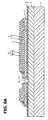
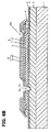
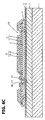
- FIGs. 6A to 6E are schematic cross-sectional views illustrating processes of manufacturing the semiconductor light emitting apparatus. Description will be made, focusing on differences from the first embodiment. The processes up to forming the recess CV described with reference to Fig. 1F are the same as the processes according to the first embodiment.
- the insulating floating layer 12 is formed in a state in which the columnar n-side via electrode is not formed in the recess CV. No n-side via electrode is formed.
- the insulating floating layer 12 is formed to extend in the hole HL and also into the recess CV, covering the pn junction region exposed at the side surface of the recess CV, and to be opened at the bottom of the recess CV to expose the n-type semiconductor layer 2.
- Same materials, film forming methods, and patterning methods as those of the first embodiment can be used for the insulating floating layer 12, for example.
- the contact hole CH is formed in the same manner as the process described with reference to Fig. 1I according to the first embodiment.
- an n-side highly reflective layer 13 is formed, covering the inside surface of the recess CV. Same materials, film forming methods, and patterning methods as those of the first embodiment can be used for the n-side highly reflective layer 13, for example.
- electrical connection with the n-type semiconductor layer 2 is secured by the n-side highly reflective layer 13 without using the columnar n-side via electrode.
- the n-side highly reflective layer 13 according to the second embodiment becomes the connection electrode contacting the n-type semiconductor layer 2 at the bottom of the recess CV and also functions as a highly reflective layer on the n-side electrode side.
- the structure in which the peripheral portion of the n-side highly reflective layer 13 overlaps with the peripheral portion of the p-side electrode layer 5 that defines the hole HL in plan view is the same as the first embodiment.
- n-side cap layer 14 (the connection electrode layers 14n and 14p) is formed at the same time similar to the process illustrated in Fig. 1K .
- the n-side highly reflective layer 13 and the n-side connection electrode 14n form the n-side electrode En of the element.
- the p-side electrode layer 5, the p-side highly reflective cap layer 9, and the p-side connection electrode 14p form the p-side electrode Ep of the element.
- Fig. 6E illustrates the semiconductor light emitting apparatus according to the second embodiment in a state as completed by forming the sealing resin layer 45 (including fluorescent powders).
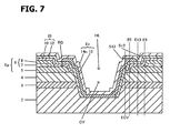
- Fig. 7 is an elevated cross-section illustrating the portion in the vicinity of the n-side highly reflective layer of the semiconductor light emitting element according to the second embodiment, and corresponds to Fig. 3A of the first embodiment.
- the schematic plane structure of the dispositions of the n-side highly reflective layer and so on are common to Figs. 3B and 3C as described in the first embodiment.
- the recess CV that exposes the n-type semiconductor layer 2 at the bottom is formed in the hole HL formed in the p-side electrode layer 5.
- the n-side highly reflective layer 13 according to the second embodiment contacts the n-type semiconductor layer 2 at the bottom of the recess CV.
- the n-side highly reflective layer 13 is formed to have the peripheral portion which overlaps the peripheral portion of the p-side electrode Ep defining the hole HL, and does not overlap the p-side highly reflective cap layer 9.
- the n-side cap layer 14n overlaps the p-side highly reflective cap layer 9 in plan view.
- the inter-electrode insulating layer IS is formed to ride on the upper surface of the p-side highly reflective cap layer 9 in the region outside the edge E9.
- a height S13 of the upper surface of the peripheral portion of the n-side highly reflective layer 13 riding on the region RG is lower than a height S12 of the upper surface of the inter-electrode insulating layer IS in the region outside the edge E9.
- the semiconductor light emitting element according to the second embodiment in similar manner to the semiconductor light emitting element of the first embodiment, the light incident from the light emitting layer is reflected by the n-side highly reflective layer 13 inside the hole and by the p-side electrode Ep outside the hole, enhancing the light extracting efficiency. Additionally, color unevenness and the like in the edge portion of the light emitting surface can be prevented, in similar manner to the semiconductor light emitting element according to the first embodiment described with reference to Figs. 5A and 5B .
- connection electrodes for providing electrical conduction to the n-type semiconductor layer are disposed in the element. If the number of n-side connection electrodes is increased and the number of columnar via electrodes according to the first embodiment becomes multiple, there is a possibility that stress applied to the element semiconductor layer caused by the thermal deformation of the columnar via electrodes accompanied by driving the element becomes large.
Landscapes
- Led Devices (AREA)
- Led Device Packages (AREA)
Abstract
Description
- The present invention relates to a semiconductor light emitting apparatus.
- The semiconductor light emitting apparatus has a semiconductor lamination including an n-type semiconductor layer and a p-type semiconductor layer, an n-side electrode electrically connected to the n-type semiconductor layer, and a p-side electrode electrically connected to the p-type semiconductor layer. For example, if a p-side electrode is formed on the p-type semiconductor layer, a recess exposing the n-type semiconductor layer is formed from the side of the p-type semiconductor layer, and an n-side electrode is formed on the recess, the n-side electrode and the p-side electrode can be disposed on the same side of the semiconductor lamination (for example, see Japanese Laid-open Patent Publication No.
2011-066304 2011-249501 2011-199221 - An object of the embodiment is to provide a semiconductor light emitting apparatus having a novel electrode structure.
- According to an aspect of the embodiment, there is provided a semiconductor light emitting apparatus, comprising:
- a first semiconductor layer of a first conductivity type;
- a light emitting layer formed on the first semiconductor layer;
- a second semiconductor layer of a second conductivity type opposite to the first conductivity type, formed on the light emitting layer and having an upper surface;
- recess formed from the upper surface of the second semiconductor layer, penetrating through the second semiconductor layer and the light emitting layer and exposing the first semiconductor layer at bottom;
- a first electrode electrically connected to the first semiconductor layer at the bottom of the recess and extending upward to extend above the upper surface of the second semiconductor layer;
- a second electrode electrically connected to the upper surface of the second semiconductor layer and having an opening which surrounds the recess in plan view and through which the first electrode extends from the inside of the recess to above the upper surface of the second semiconductor layer; and
- an insulating layer disposed between the first and second electrodes above the upper surface of the second semiconductor layer;
- wherein the second electrode constitute a reflective electrode that reflects light incident from the light emitting layer side,
- wherein the first electrode includes a reflective electrode layer formed covering the opening in plan view, that reflects light incident from the light emitting layer side, and
- wherein the reflective electrode layer of the first electrode has a peripheral portion overlapping a peripheral portion of the second electrode defining the opening in plan view.
- The light extracting efficiency can be enhanced by forming the light reflective electrode layer of the first electrode overlapping the second electrode at the peripheral portion.
-
-
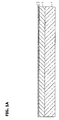
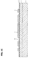
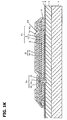
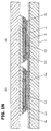
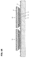
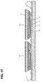
Figs. 1A to 1V are cross-sectional views schematically illustrating a manufacturing method of a semiconductor light emitting apparatus according to a first embodiment. -
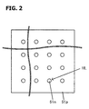
Fig. 2 is a plan view schematically illustrating a plane structure of contact portions of p-side electrodes and n-side electrodes with a semiconductor layer in a semiconductor light emitting element according to an embodiment. -
Fig. 3A is a cross-sectional view schematically illustrating structure in the vicinity of an n-side highly reflective layer of the semiconductor light emitting element according to the first embodiment, andFigs. 3B and 3C are plan views schematically illustrating arrangement of the n-side highly reflective layer according to the first embodiment. -
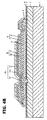
Figs. 4A to 4C are schematic cross-sectional views illustrating processes of manufacturing a semiconductor light emitting apparatus according to a comparative example. -
Figs. 5A and 5B are schematic cross-sectional views illustrating structures in the vicinity of the n-side via electrodes of the light emitting apparatuses according to the first embodiment and the comparative example. -
Figs. 6A to 6E are schematic cross-sectional views illustrating processes of manufacturing a semiconductor light emitting apparatus according to a second embodiment. -
Fig. 7 is a schematic cross-sectional view illustrating structure in the vicinity of the n-side highly reflective layer of the semiconductor light emitting element according to the second embodiment. - First, a semiconductor light emitting apparatus according to a first embodiment of the invention will be described.
Figs. 1A to 1L are schematic cross-sectional views illustrating processes of manufacturing a semiconductor light emitting element according to the first embodiment. In the present embodiment, a nitride-series semiconductor light emitting element is formed. Here, the term "nitride series" means compound including nitrogen as group V element. For example, a metal organic chemical vapor deposition (MOCVD) is used as a method of growing a semiconductor layer. A plurality of light emitting elements is formed at the same time on one growth substrate.Figs. 1A to 1L illustrate process of manufacturing representative one element. - As illustrated in
Fig. 1A , a sapphire substrate is prepared as agrowth substrate 1. Thegrowth substrate 1 is loaded in an MOCVD apparatus, and thermal cleaning is performed. A GaN buffer layer and an undoped GaN layer are grown on a cleaned substrate, and then an n-type GaN layer 2 doped with n-type impurity such as Si and having a film thickness of about 5 µm is grown. InFig. 1A and other figures, the GaN buffer layer and the undoped GaN layer are collectively illustrated as the n-type GaN layer 2. - A light emitting layer (active layer) 3 is grown on the n-
type GaN layer 2. A multiple quantum well structure including, for example, InGaN layers as well layers, and GaN layers as barrier layers alternately laminated, is formed as thelight emitting layer 3. A p-type GaN layer 4 doped with p-type impurity such as Mg and having a film thickness of about 0.5 µm is grown on thelight emitting layer 3. - The
growth substrate 1 is a single-crystal substrate having a lattice constant that enables epitaxial growth of GaN. A material is selected from those which are transparent to the light at a wavelength of 362 nm, absorption edge wavelength of GaN, so that the substrate can be peeled off by laser lift-off in a later process. Spinel, SiC, ZnO, and the like may be used, as well as sapphire. - As illustrated in
Fig. 1B , a reflective metal layer, for example formed of Ag added with additive such as as Ni, Pt, Ti, or Pd and having a thickness of 200 nm is deposited by electron beam vapor deposition on the p-type GaN layer 4, and is patterned by lift-off to form a p-side electrode 5 of desired shape. It is preferable that the p-side electrode layer 5 includes one material selected from the group consisting of Ag, Pt, Ni, Al, Pd, and alloys thereof, so as to serve as a reflective electrode. -
Fig. 2 is a schematic plan view illustrating a plane structure of contact portions of p-side electrodes 51p and n-side electrodes 51n with semiconductor layers in the semiconductor light emitting element of embodiment. The p-side electrode 51p is formed spreading on the upper surface of the p-type semiconductor layer. Holes HL are formed to distribute discretely in the p-side electrode 51p, for example, in matrix shape. Inside each hole HL, an n-side electrode (via electrode) 51n is disposed. One element may have a rectangular shape having, for example, a size of about 600 µm x 1300 µm. The number of viaelectrodes 51n arranged in one element is, for example, about 40. -
Fig. 1B and other figures representatively illustrate processes of forming one n-side via electrode and illustrate one hole HL formed in the p-side electrode layer 5. - As illustrated in
Fig. 1C , afringe layer 6 is formed by depositing an SiO2 layer having a film thickness equal to the thickness of the p-side electrode layer 5, for example, by sputtering on the p-type GaN layer 4 outside the p-side electrode layer 5 so as to surround the circumference of the p-side electrode layer 5. - As illustrated in
Fig. 1D , on upper surfaces of the p-side electrode layer 5 and thefringe layer 6, and on the p-type GaN layer 4 between the p-type electrode layer 5 and thefringe layer 6, an Ag layer of a thickness of 100 nm which will become a highly reflective layer is deposited for example by sputtering, and successively TiW/ Ti/ Pt/ Au/ Ti lamination (left side layer is formed on the substrate side or lower side, to represent laminated structure), which will become diffusion preventing layer, is formed with thicknesses 250 nm/ 50 nm/ 100 nm/ 1000 nm/ 30 nm for example by sputtering, and the lamination is patterned by lift-ofF, to form a p-side highlyreflective cap layer 9. - The p-
side electrode layer 5 is doped with additive such as Ni, Pt, Ti, or Pd to enhance ohmic contact with the p-type GaN layer 4. In contrast, no additive is doped to the p-side highlyreflective layer 7. - The p-side
diffusion preventing layer 8 serves to prevent diffusion of elements used in the p-side electrode layer 5 and the p-side highlyreflective layer 7. When the p-side electrode layer 5 and the p-side highlyreflective layer 7 include Ag, the p-side diffusionpreventive layer 8 can use Ti, W, Pt, Pd, Mo, Ru, Ir, Au, and an alloy thereof. - The p-side highly
reflective cap layer 9 is not formed in the vicinity of the edge of the hole HL, and the edge of the p-side highlyreflective cap layer 9 on the side of the hole HL is disposed to be separated from the edge of the hole HL to the outer side. The peripheral portion of the p-side diffusionpreventive layer 8 is formed to cover the peripheral portion of the p-side highlyreflective cap layer 9. In plan view, the edge of the p-side diffusionpreventive layer 8 is disposed inside the edge of the p-side highlyreflective layer 7. - At the edge of the p-side highly
reflective cap layer 9 on the circumference side of the element, the edge of the p-side highlyreflective layer 7 coincides with the edge of the p-side diffusionpreventive layer 8, and is disposed on the upper surface of thefringe layer 6. The structure in which the edge of the p-side highlyreflective cap layer 9 is disposed on the upper surface of thefringe layer 6, i.e. separated from the semiconductor layers 2, 3, and 4 functions as a leakage stopper of Ag in the p-side highlyreflective cap layer 9. - As illustrated in
Fig. 1E , an insulatingcap layer 10 is formed by depositing an SiO2 film having a thickness of 300 nm, covering the p-side highlyreflective cap layer 9, the p-side electrode layer 5, and thefringe layer 6, for example by sputtering, and is patterned by lift-off. As the patterning method, dry etching using CF4-based gas, for example, can be used after forming a layer of SiO2 on the entire surface, as well as the lift-off. - The insulating
cap layer 10 has a function of preventing leakage of the Ag-based material used in the p-side electrode layer 5 and the p-side highlyreflective layer 7 of the p-side highlyreflective cap layer 9. An insulating material such as SiO2, or SiN can also be used. - The insulating
cap layer 10 is formed to cover the edge of the hole HL and to extend on the side surface of the p-side electrode layer 5 that defines the hole HL. The side surfaces of the p-side electrode layer 5 are covered with the insulatingcap layer 10. The insulatingcap layer 10 has a corresponding opening OP in the hole HL, and the p-type GaN layer 4 is exposed at the bottom of the opening OP. - As illustrated in
Fig. 1F , the p-type GaN layer 4 exposed in the opening OP of the insulatingcap layer 10 and thelight emitting layer 3 therebelow are removed by, for example, reactive ion etching (RIE), to expose the n-type GaN layer, forming a recess CV which provides a contact area for an n-side electrode. The insulatingcap layer 10 functions as an etching mask. - As illustrated in
Fig. 1G , an n-side viaelectrode 11 is formed on the n-type GaN layer 2 exposed at the bottom of the recess CV, using lift-off, using, for example Al, or preferably Ag or an Ag alloy from the viewpoint of high reflectance. ATi film 11p having a thickness of 1 nm may be vapor deposited under the Ag or Ag alloy layer as a contact material with the n-type GaN layer 2 to provide appropriate contact resistance and high reflectance. - For example, the diameter of one hole HL formed in the p-
side electrode layer 5 is about 40 µm, the diameter of the edge of the recess CV is about 35 µm, and the diameter of the bottom portion of the viaelectrode 11 is about 30 µm. - As illustrated in
Fig. 1H , an insulating floatinglayer 12 is formed by depositing an SiO2 film having a thickness of 600 nm by sputtering, covering the p-side electrode layer 5, thefringe layer 6, the p-side highlyreflective cap layer 9, and the insulatingcap layer 10, and patterning by lift-off or dry etching using CF4-based gas. An insulating material such as SiO2, or SiN can be used, as a material of the floatinglayer 12. - The insulating floating
layer 12 is formed to extend to the inside of the opening OP and the recess CV, covering the pn junction region exposed to the side surface of the recess CV. The insulating floatinglayer 12 has an opening on the upper surface of the n-side viaelectrode 11. An inter-electrode insulating layer IS between the p-side and the n-side electrodes is formed by the lamination of the insulatingcap layer 10 and the insulating floatinglayer 12. The inter-electrode insulating layer IS is interposed between a p-side electrode Ep and an n-side electrode En to be completed by the later process, and electrically separates the p-side electrode Ep and the n-side electrode En. - As illustrated in
Fig. 1I , a contact hole CH for connecting the p-side electrode is formed by removing a partial region of the inter-electrode insulating layer IS, for example, in the vicinity of the edge portion of the element, for example, by RIE, and exposing the upper surface of the p-side highlyreflective cap layer 9. - As illustrated in
Fig. 1J , an n-side highlyreflective layer 13 is formed by depositing Ag/ Ti/ Pt/ Au layers respectively having thicknesses of 200 nm, 100 nm, 200 nm, and 200 nm on the n-side viaelectrode 11, for example, by electron beam deposition or sputtering, and by patterning using lift-off. A function of reflecting light progressing from the lower side through the insulatinglayers type semiconductor layer 2 side is provided. Further, aTi layer 13p may be formed as an undercoat of the Ag layer in order to enhance the adhesion with the insulatinglayer 12. However, the reflectance is reduced by Ti, so the thickness of theTi layer 13p is preferably selected 5 nm or less, for example, 1 nm. - In plan view, the n-side highly
reflective layer 13 is formed so that the peripheral portion of the n-side highlyreflective layer 13 overlaps the peripheral portion of the p-side electrode layer 5 which defines the hole HL. Details of the arrangement of the n-side highlyreflective layer 13 with related elements will be described with reference toFig. 3A . - As illustrated in
Fig. 1K , a conductive layer 14 divided in n-side portion and p-side portion, is formed by depositing Ti/ Pt/ Au layers respectively having thicknesses of 50 nm, 100 nm, and 400 nm by electron beam deposition or sputtering, and performing patterning by lift-off. - Portion of the conductive layer 14 which extends from above the n-side highly
reflective layer 13 onto the inter-electrode insulating layer IS covering the p-side highlyreflective cap layer 9 forms an n-side cap layer (n-side connection electrode) 14n. The n-side viaelectrode 11, the n-side highlyreflective layer 13, and the n-side cap layer 14n form the n-side electrode En of the element. - Portion of the conductive layer 14 which is formed in the contact hole CH and is electrically separated from the n-
side cap layer 14n by interposing a gap from the n-side cap layer 14n forms a p-side connection electrode 14p. The p-side electrode layer 5, the p-side highlyreflective cap layer 9, and the p-side connection electrode 14p form the p-side electrode Ep of the element. - As illustrated in
Fig. 1L , street ST is formed by removing the p-type semiconductor layer 4, thelight emitting layer 3, and the n-type semiconductor layer 2 in a region between neighboring elements by RIE using, for example, chlorine gas, using a photoresist mask, exposing thegrowth substrate 1, and separating the neighboring elements. In this manner, the semiconductor light emitting element according to the first embodiment is formed. - With reference to
Figs. 3A to 3C , structure in the vicinity of the n-side highlyreflective layer 13 of the semiconductor light emitting element according to the first embodiment will be described.Fig. 3A is a schematic cross-sectional view illustrating a portion in the vicinity of the n-side highlyreflective layer 13, andFigs. 3B and 3C are schematic plan views illustrating plane arrangement of the n-side highlyreflective layer 13 and related elements. - The hole HL is formed in the p-
side electrode layer 5 of the p-side electrode Ep. The recess CV is formed by using the insulatingcap layer 10 covering the p-side electrode as an etching mask and exposes the n-type semiconductor layer 2 at the bottom. The n-side viaelectrode 11 is formed on the n-type semiconductor layer 2 in the recess CV. In plan view, edge E9 of the p-side highlyreflective cap layer 9 surrounding the hole HL is located on outer side (with respect to the hole HL) than edge E5 of the p-side electrode layer 5 that defines the hole HL. In plan view, the edge E5 of the hole HL surrounds upper edge ECV of the recess CV formed in the semiconductor layers 2, 3, and 4. - The p-side electrode Ep has a flat region RG formed by an upper surface of the p-
side electrode layer 5 inside (with respect to the hole HL) the edge E9 of the p-side highlyreflective cap layer 9. A peripheral portion of the n-side highlyreflective layer 13 is formed on the inter-electrode insulating layer IS formed on the flat region RG. In plan view, the n-side highlyreflective layer 13 covers the hole HL and overlaps a peripheral portion of the p-side electrode layer 5. Edge E13 of the n-side highlyreflective layer 13 is located outside the edge E5 of the p-side electrode layer 5 and is located inside the edge E9 of the p-side highlyreflective cap layer 9. - The n-side highly
reflective layer 13 and the p-side highlyreflective cap layer 9 do not overlap each other.Fig. 3B illustrates the n-side highlyreflective layer 13 by left side lowering hatching, and the p-side electrode layer 5 and the p-side highlyreflective cap layer 9 by right side lowering hatching. The overlapped portion between the n-side highlyreflective layer 13 and the p-side electrode layer 5 is cross-hatched. The width WD of the cross-hatched portion in which peripheral portions of the n-side highlyreflective layer 13 and the p-side electrode Ep are overlapped with each other is preferably 25 µm or less, for example. - In plan view, the n-
side cap layer 14n is formed to cross the edge E13 of the n-side highlyreflective layer 13 and also cross the edge E9 of the p-side highlyreflective cap layer 9, and overlaps the p-side highlyreflective cap layer 9. InFig. 3C , the n-side cap layer 14n is illustrated by left side lowering hatching. - The inter-electrode insulating layer IS is formed to ride on a portion of the upper surface of the p-side highly
reflective cap layer 9. A height S13 of the upper surface of the peripheral portion of the n-side highlyreflective layer 13 riding on the flat region RG inside the edge E9 is lower than a height S12 of the upper surface of the inter-electrode insulating layer IS outside the edge E9. - Remaining processes of manufacturing the semiconductor light emitting apparatus according to the first embodiment will be described with reference to
Figs. 1M to 1V. Figs. 1M to 1V are schematic cross-sectional views illustrating the processes of manufacturing the semiconductor light emitting apparatus according to the first embodiment. - As illustrated in
Fig. 1M , for example, a silicon substrate is prepared as a supportingsubstrate 21. An SiO2 insulating layer 22 is formed by thermal oxidation. The supportingsubstrate 21 is preferably formed with a material having a thermal expansion coefficient close to sapphire (7.5 x 10⁻⁶/ K) or GaN (5.6 x 10⁻⁶/ K) and high thermal conductivity. Examples include Si, AIN, Mo, W, and CuW. The thickness of the insulatinglayer 22 may be a thickness that can achieve an object of securing insulation. - For example, a fusion or melt
layer 23 which will form electrode is formed on the supporting substrate by depositing an AuSn (Sn: 20 wt%) having a thickness of 1 µm by, for example, resistance heating vapor deposition on the insulatinglayer 22. Thesupport substrate electrodes 23 will be adhered to the n-side connection electrode 14n and the p-side connection electrode 14p on the element. Examples of materials of thesupport substrate electrode 23, the n-side connection electrode 14n, and the p-side connection electrode layer 14p which become bonded adhesion layers include metals including Au-Sn, Au-In, Pd-In, Cu-In, Cu-Sn, Ag-Sn, Ag-In, and Ni-Sn which can be joined by fusion or melt joining and metals including Au, which can be joined by diffusion joining. - As illustrated in
Fig. 1N , in the present example, processes of manufacturing a light emitting apparatus having a structure in which twolight emitting elements - On the
support substrate 21, there are formedelectrode layer 23p to be connected to the p-side electrode EpA of thelight emitting element 31A, electrode layer 23np to be connected to the n-side electrode EnA of thelight emitting element 31A and the p-side electrode EpB of thelight emitting element 31B, andelectrode layer 23n to be connected to the n-side electrode EnB of thelight emitting element 31B, in a manner of being electrically separated from each other. - The
support substrate electrodes 23p, 23np, and 23n, the n-sideconnection electrode layer 14n, and the p-side connection electrode layer 14p of each element are aligned and adhered, for example, heated to 300°C in a state of applying pressure to 3 MP, and maintained for 10 minutes. Thereafter, the fusion joining is performed by cooling the resultant to room temperature. - In this manner, the electric connection structure in which the p-side electrode EpA of the
light emitting element 31A by theelectrode layer 23p is extracted, the n-side electrode EnA of thelight emitting element 31A and the p-side electrode EpB of thelight emitting element 31B are connected in series by the electrode layer 23np, and the n-side electrode EnB of thelight emitting element 31B is extracted by theelectrode layer 23n is formed. - As illustrated in
Fig. 1O , thegrowth substrate 1 is peeled off using laser lift-off by radiating, for example, a UV laser beam UVL from the rear side of thesapphire substrate 1, and decomposing the buffer layer by heating. Methods such as etching or the like may also be used for peeling off or removing thegrowth substrate 1. - Subsequently, Ga generated by the laser lift-off is removed by hot water and the like, and the surface is treated by a hydrochloric acid or the like. According to this, the n-
type GaN layer 2 is exposed. The surface treatment may be a method that can etch a nitride semiconductor, and an agent such as acids such as phosphoric acid and sulfuric acid and alkali such as KOH and NaOH can be used. Additionally, the surface treatment may be performed by dry etching using Ar plasma or chlorine-based plasma, polishing, or the like. Further, the surface of the n-type GaN layer 2 is subjected to a Cl or Ar treatment using an apparatus for dry etching such as RIE or a smoothing treatment using a CMP polishing apparatus to remove a laser mark or a laser damaged layer. - As illustrated in
Fig. 1P , a light extracting structure or a micro-cone structure is formed by immersing the surface of the exposed n-type GaN layer 2, for example, in an alkaline solution such as a KOH solution to perform unevenness forming process , to form unevenness unique to crystal structure on the surface of the n-type GaN layer 2, enhancing light extracting efficiency. - As illustrated in
Fig. 1Q , a glarelight absorption layer 24 is formed in the outer edge region of theelectrodes - The glare
light absorption layer 24 is formed with aperture at wire bonding region, exposes an AuSn layer of a supportingsubstrate electrode 23, and covers the outer region of the opening with the Ti layer. The Ti layer easily absorbs yellow light generated in the fluorescent layer formed by covering the element, compared to the AuSn layer. Therefore, yellow light is absorbed by theTi layer 24 in the region around the wire bonding so that color unevenness or color separation in the peripheral portion of the light emitting apparatus can be prevented. - As illustrated in
Fig. 1R , an entiresurface protection film 25 is formed by depositing SiO2 having a thickness of 350 nm on the entire upper surface of the element, for example, by chemical vapor deposition (CVD). - As illustrated in
Fig. 1S , the back surface side of the supportingsubstrate 21 is ground or polished to thin the support substrate, for example, to a thickness of 300 µm, in order to lower thermal resistance. Additionally, a rearsurface metal layer 26 is formed by depositing Ti/ Pt/ Au respectively having thicknesses of 50 nm, 15 nm, and 200 nm, for example, by electron beam deposition on the ground or polished surface of the supportingsubstrate 21, in order to secure adhesion between the mounting substrate and the joining material. - As illustrated in
Fig. 1T , the supportingsubstrate 21 is divided by a laser scribe or dicing 27. - As illustrated in
Fig. 1U , by using a bonding or joiningmaterial 42 such as an Ag paste or AuSn on apackage substrate 41, die bonding is performed to the supporting substrate 21connected with theelement package substrate 41. Thereafter, package mounting is completed by respectively connecting the p-side electrode of theelement 31A and the n-side electrode, of theelement 31B tocurrent supply pads package substrate 41, bywire bondings - As illustrated in
Fig. 1V , thelight emitting elements resin 45. For whitening the output light, phosphor such as yellow light emitting phosphor powders are mixed in the sealing resin. A sealingresin layer 45 is sealed, filled, and cured to form theresin layer 45. A semiconductor light emitting apparatus according to the first embodiment is thus formed. - Subsequently, the semiconductor light emitting apparatus according to a comparative example will be described.
Figs. 4A to 4C are schematic cross-sectional views illustrating processes of manufacturing the semiconductor light emitting element according to the comparative example. Hereinafter, description will continue focusing on differences from the first embodiment. The processes up to the step of forming the contact hole CH described with reference toFig. 1I are the same as the processes according to the first embodiment. - As illustrated in
Fig. 4A , the n-side highlyreflective layer 13 is formed on the n-side viaelectrode 11. The n-side highlyreflective layer 13 of the comparative example is different from that of the first embodiment in that the n-side highlyreflective layer 13 extends from on the n-side viaelectrode 11 to widely on the inter-electrode insulating layer IS covering the p-side highlyreflective cap layer 9. - As illustrated in
Fig. 4B , an n-side cap layer (connection electrode layer) 14n is formed, covering the n-side highlyreflective layer 13. As illustrated inFig. 4C , theconnection electrode layer 15p is formed. - The
connection electrode layers reflective layer 13 does not ride on the inter-electrode insulating layer IS on the p-side highly reflective cap layer 9 (seeFig. 1J ). Accordingly, it becomes easy to form theconnection electrode layers 14n and 14p on the flat upper surface of the inter-electrode insulating layer IS by the same process (to have the same film thicknesses), and to equalize the heights of the upper surfaces of theconnection electrode layers 14n and 14p (seeFig. 1K ). - According to the comparative example, the n-side highly
reflective layer 13 is formed, riding on the inter-electrode insulating layer IS. When the heights of the upper surfaces of the n-side connection electrode 14n and the p-side connection electrode 15p are to be disposed at the same level, the thickness of the n-side connection electrode 14n should be different from that of the p-side connection electrode 15p (seeFig. 4C ). Accordingly, the step of forming the n-side connection electrode 14n and the step of forming the p-side connection electrode 15p should become different processes. Additionally, it is difficult to uniformlize the heights of the films formed by different processes. - After the process of
Fig. 4C , bonding with a support substrate, packaging to a package substrate, and the like are performed, in similar manner to the processes after the process of forming the street according to the first embodiment as illustrated inFig. 1L , to provide a semiconductor light emitting apparatus according to the comparative example. - Description will be made on differences in light propagation in the elements according to the first embodiment and the comparative example, referring to
Figs. 5A and 5B. Figs. 5A and 5B are schematic cross-sectional views illustrating portions in the vicinity of the n-side via electrodes of the light emitting apparatuses according to the first embodiment and the comparative example, respectively, and conceptually illustrate light propagation in the light emitting element. Yellow light is generated from the fluorescent material by the blue light emitted from the GaNlight emitting layer 3. Yellow light LT backwardly scattered is introduced into the inter-electrode insulating layer IS in the vicinity of the n-side via electrode of the element. - As illustrated in
Fig. 5B , according to the comparative example, the n-side highlyreflective layer 13 is formed widely opposing the p-side highlyreflective cap layer 9. Accordingly, the yellow light LT introduced into the inter-electrode insulating layer IS is propagated by repeating reflection between the n-side highlyreflective layer 13 and the p-side highlyreflective cap layer 9, to be released from end surface of the element. Thus, color unevenness or color separation can occur in end portions of the light emitting surface. - As illustrated in
Fig. 5A , according to the first embodiment, the n-side highlyreflective layer 13 is narrowly formed in the region that does not face the p-side highlyreflective cap layer 9. Among the n-side electrodes, those which are formed up to a region facing the p-side highlyreflective cap layer 9, is only the n-side cap layer (n-side connection electrode) 14n. - Accordingly, the yellow light LT inserted into the inter-electrode insulating layer IS is propagated between the n-
side cap layer 14n and the p-side highlyreflective cap layer 9. However, the n-side cap layer 14n has lower reflectance of the incident light, that is, a higher light absorbing property compared to the n-side highlyreflective layer 13, and functions as a light absorbing layer. Therefore, according to the first embodiment, the propagated light can be attenuated by the incidence to the n-side cap layer 14n and color unevenness caused by the emission of the yellow light from the element edge surface and the like can be prevented. - It is preferable for the n-side highly
reflective layer 13 to use Ag, Pt, Ni, Al, Pd, an alloy thereof, to have a high reflection function. The n-side cap layer 14n is formed, for example, of lamination of Ti/ Pt/ Au layers, in which a Ti layer is formed on the semiconductor layer side of the Pt layer, that is, on the light incident side. The thickness of the Ti layer is as thick as, for example, 50 nm, and hence the incident light rarely reaches the Pt layer. - The thickness of the Ti layer of the n-
side cap layer 14n is preferably 20 nm or more (for example, 50 nm), in which function of absorbing light is enhanced. Here, TiN, Ni, Cr, or the like can be used, as well as Ti, as a material having the high light absorbing property. - In the structure according to the comparative example, since the n-side highly
reflective layer 13 that includes easily migrating Ag is widely formed, the leakage easily occurs. In the structure according to the first embodiment, the n-side highlyreflective layer 13 is more narrowly formed than that according to the comparative example. Therefore, there is an effect of restraining migration or leakage of Ag atoms. - As described above, the semiconductor light emitting element according to the first embodiment has the n-side highly
reflective layer 13 serving as a reflective electrode formed as part of the n-side electrode En and the p-side electrode Ep formed as a reflecting electrode extending widely over the total area in such a manner that the peripheral portions of the n-side highlyreflective layer 13 and the p-side electrode Ep around the hole overlap each other. Accordingly, light incident from the light emitting layer can be reflected by the n-side highlyreflective layer 13 inside the hole and by the p-side electrode Ep outside the hole. Therefore, the light extracting efficiency can be enhanced. - Due to the facts that the overlapping of the n-side highly
reflective layer 13 and the hole forming portion of the p-side electrode Ep is limited to peripheral portions, and that the n-side cap layer 14n serving as a light absorbing layer having a higher light absorbing property than the n-side highlyreflective layer 13 is formed extending to the outside of the n-side highlyreflective layer 13 as another portion of the n-side electrode En, light generated in the fluorescent layer and penetrated into the element is prevented from being propagated by repetitive reflection at the n-side highlyreflective layer 13, and generation of color unevenness in the edge portion of the light emitting surface can be prevented. - A semiconductor light emitting apparatus according to the second embodiment will be described.
Figs. 6A to 6E are schematic cross-sectional views illustrating processes of manufacturing the semiconductor light emitting apparatus. Description will be made, focusing on differences from the first embodiment. The processes up to forming the recess CV described with reference toFig. 1F are the same as the processes according to the first embodiment. - As illustrated in
Fig. 6A , unlike the first embodiment, the insulating floatinglayer 12 is formed in a state in which the columnar n-side via electrode is not formed in the recess CV. No n-side via electrode is formed. The insulating floatinglayer 12 is formed to extend in the hole HL and also into the recess CV, covering the pn junction region exposed at the side surface of the recess CV, and to be opened at the bottom of the recess CV to expose the n-type semiconductor layer 2. Same materials, film forming methods, and patterning methods as those of the first embodiment can be used for the insulating floatinglayer 12, for example. - As illustrated in
Fig. 6B , the contact hole CH is formed in the same manner as the process described with reference toFig. 1I according to the first embodiment. - As illustrated in
Fig. 6C , an n-side highlyreflective layer 13 is formed, covering the inside surface of the recess CV. Same materials, film forming methods, and patterning methods as those of the first embodiment can be used for the n-side highlyreflective layer 13, for example. According to the second embodiment, electrical connection with the n-type semiconductor layer 2 is secured by the n-side highlyreflective layer 13 without using the columnar n-side via electrode. The n-side highlyreflective layer 13 according to the second embodiment becomes the connection electrode contacting the n-type semiconductor layer 2 at the bottom of the recess CV and also functions as a highly reflective layer on the n-side electrode side. The structure in which the peripheral portion of the n-side highlyreflective layer 13 overlaps with the peripheral portion of the p-side electrode layer 5 that defines the hole HL in plan view is the same as the first embodiment. - As illustrated in
Fig. 6D , n-side cap layer 14 (theconnection electrode layers 14n and 14p) is formed at the same time similar to the process illustrated inFig. 1K . According to the second embodiment, the n-side highlyreflective layer 13 and the n-side connection electrode 14n form the n-side electrode En of the element. Similar to the first embodiment, the p-side electrode layer 5, the p-side highlyreflective cap layer 9, and the p-side connection electrode 14p form the p-side electrode Ep of the element. - After the process of
Fig. 6D , bonding with the supporting substrate, mounting to the package substrate, and so on are performed in similar manner the first embodiment as illustrated inFig. 1L and on. The semiconductor light emitting apparatus according to the second embodiment is thus formed. -
Fig. 6E illustrates the semiconductor light emitting apparatus according to the second embodiment in a state as completed by forming the sealing resin layer 45 (including fluorescent powders). -
Fig. 7 is an elevated cross-section illustrating the portion in the vicinity of the n-side highly reflective layer of the semiconductor light emitting element according to the second embodiment, and corresponds toFig. 3A of the first embodiment. The schematic plane structure of the dispositions of the n-side highly reflective layer and so on are common toFigs. 3B and 3C as described in the first embodiment. - The recess CV that exposes the n-
type semiconductor layer 2 at the bottom is formed in the hole HL formed in the p-side electrode layer 5. The n-side highlyreflective layer 13 according to the second embodiment contacts the n-type semiconductor layer 2 at the bottom of the recess CV. - In plan view, in the same manner as the structure described in the first embodiment, the n-side highly
reflective layer 13 is formed to have the peripheral portion which overlaps the peripheral portion of the p-side electrode Ep defining the hole HL, and does not overlap the p-side highlyreflective cap layer 9. The n-side cap layer 14n overlaps the p-side highlyreflective cap layer 9 in plan view. - In the same manner as in the first embodiment, the inter-electrode insulating layer IS is formed to ride on the upper surface of the p-side highly
reflective cap layer 9 in the region outside the edge E9. A height S13 of the upper surface of the peripheral portion of the n-side highlyreflective layer 13 riding on the region RG is lower than a height S12 of the upper surface of the inter-electrode insulating layer IS in the region outside the edge E9. - In the semiconductor light emitting element according to the second embodiment, in similar manner to the semiconductor light emitting element of the first embodiment, the light incident from the light emitting layer is reflected by the n-side highly
reflective layer 13 inside the hole and by the p-side electrode Ep outside the hole, enhancing the light extracting efficiency. Additionally, color unevenness and the like in the edge portion of the light emitting surface can be prevented, in similar manner to the semiconductor light emitting element according to the first embodiment described with reference toFigs. 5A and 5B . - As described with reference to
Fig. 2 , a plurality of connection electrodes for providing electrical conduction to the n-type semiconductor layer are disposed in the element. If the number of n-side connection electrodes is increased and the number of columnar via electrodes according to the first embodiment becomes multiple, there is a possibility that stress applied to the element semiconductor layer caused by the thermal deformation of the columnar via electrodes accompanied by driving the element becomes large. The layered n-side electrode structure serving also as highly reflective layer, without using columnar via electrodes as the connection electrodes, similar to the second embodiment, is expected to provide effect of preventing stress. Additionally, process of forming the columnar via electrode may be omitted. - The invention has been described along the embodiments, but the invention is not limited thereto. For example, it is obvious to those skilled in the art that various modifications, improvements, combinations, and the like are possible.
Claims (13)
- A semiconductor light emitting apparatus, comprising:a first semiconductor layer of a first conductivity type;a light emitting layer formed on the first semiconductor layer;a second semiconductor layer of a second conductivity type opposite to the first conductivity type, formed on the light emitting layer and having an upper surface;recess formed from the upper surface of the second semiconductor layer, penetrating through the second semiconductor layer and the light emitting layer and exposing the first semiconductor layer at bottom;a first electrode electrically connected to the first semiconductor layer at the bottom of the recess and extending upward to extend above the upper surface of the second semiconductor layer;a second electrode electrically connected to the upper surface of the second semiconductor layer and having an opening which surrounds the recess in plan view and through which the first electrode extends from the inside of the recess to above the upper surface of the second semiconductor layer; andan insulating layer disposed between the first and second electrodes above the upper surface of the second semiconductor layer;wherein the second electrode constitute a reflective electrode that reflects light incident from the light emitting layer side,wherein the first electrode includes a reflective electrode layer formed covering the opening in plan view, that reflects light incident from the light emitting layer side, andwherein the reflective electrode layer of the first electrode has a peripheral portion overlapping a peripheral portion of the second electrode defining the opening in plan view.
- The semiconductor light emitting apparatus according to claim 1,
wherein the first electrode further includes a light absorbing electrode layer formed on the reflective electrode layer and having a lower reflectance against incident light from the light emitting layer side than that of the reflective electrode layer, and
wherein the light absorbing electrode layer is formed to spread to outer area than the peripheral portion of the reflective electrode layer in plan view. - The semiconductor light emitting apparatus according to claim 1,
wherein the first electrode includes a contact electrode connected to the first semiconductor layer at the bottom of the recess and extends upward, and the reflective electrode layer. - The semiconductor light emitting apparatus according to claim 1,
wherein the second electrode includes a first layer and a second layer formed on the first layer, the opening is defined by first periphery of the first layer, and the second layer has second periphery surrounding the opening and disposed on outer side of the opening than the first periphery, and
wherein the reflective electrode layer of the first electrode has a third periphery disposed between the first and the second peripheries in plan view. - The semiconductor light emitting apparatus according to claim 4,
wherein the light absorbing electrode layer of the first electrode is formed to spread in outer area than the second periphery of the second layer of the second electrode, and overlaps the second layer in plan view. - The semiconductor light emitting apparatus according to claim 1,
wherein the reflective electrode layer of the first electrode is in contact with the first semiconductor layer at the bottom of the recess. - The semiconductor light emitting apparatus according to claim 6,
) wherein the insulating layer includes a first insulating layer covering a side surface of the recess and the second electrode, and exposing a bottom surface of the recess, and
wherein the reflective electrode layer of the first electrode contacts the first semiconductor layer exposed at the bottom of the recess, and extends on portions of the first insulating layer on the side surface of the recess and on the second semiconductor layer and extends to a portion overlapping the second electrode. - The semiconductor light emitting apparatus according to claim 1,
wherein the first semiconductor layer and the second semiconductor layer are compound semiconductor layers including GaN and the light emitting layer has a multiple quantum well structure of a compound semiconductor layer including GaN. - The semiconductor light emitting apparatus according to claim 8,
wherein the second electrode includes an Ag undermost layer including additive and another Ag layer disposed thereon and not including additive. - The semiconductor light emitting apparatus according to claim 9,
wherein the first electrode includes a light reflecting layer having a high reflectance and a contact layer disposed between the light reflecting layer and the first semiconductor layer and having a lower reflectance than the light reflecting layer. - The semiconductor light emitting apparatus according to claim 10, further comprising:a sealing resin layer covering the second semiconductor layer, the first electrode, and the second electrode; andphosphor mixed in the sealing resin layer.
- A semiconductor light emitting apparatus, comprising:a first semiconductor light emitting element;a second semiconductor light emitting element; anda supporting substrate formed with supporting electrodes, wherein the first semiconductor light emitting element includes:a first semiconductor layer of a first conductivity type;a first light emitting layer formed on the first semiconductor layer;a second semiconductor layer of a second conductivity type opposite to the first conductivity type, formed on the first light emitting layer and having a first upper surface;first recess formed from the first upper surface of the second semiconductor layer, penetrating through the second semiconductor layer and the first light emitting layer and exposing the first semiconductor layer at bottom;a first electrode electrically connected to the first semiconductor layer at the bottom of the recess and extending upward to extend above the first upper surface of the second semiconductor layer;a second electrode electrically connected to the first upper surface of the second semiconductor layer and having a first opening which surrounds the first recess in plan view and through which the first electrode extends from the inside of the first recess to above the first upper surface of the second semiconductor layer; anda first insulating layer disposed between the first and second electrodes above the first upper surface of the second semiconductor layer;wherein the second electrode constitute a reflective electrode that reflects light incident from the first light emitting layer side,wherein the first electrode includes a first reflective electrode layer formed covering the first opening in plan view, that reflects light incident from the first light emitting layer side, andwherein the first reflective electrode layer of the first electrode has a peripheral portion overlapping a peripheral portion of the second electrode defining the first opening in plan view, and wherein the second semiconductor light emitting element includes:a third semiconductor layer of a first conductivity type;a second light emitting layer formed on the third semiconductor layer;a fourth semiconductor layer of a second conductivity type opposite to the first conductivity type, formed on the second light emitting layer and having a first upper surface;second recess formed from the first upper surface of the fourth semiconductor layer, penetrating through the fourth semiconductor layer and the second light emitting layer and exposing the third semiconductor layer at bottom;a third electrode electrically connected to the third semiconductor layer at the bottom of the recess and extending upward to extend above the first upper surface of the fourth semiconductor layer;a fourth electrode electrically connected to the first upper surface of the fourth semiconductor layer and having a first opening which surrounds the second recess in plan view and through which the third electrode extends from the inside of the second recess to above the first upper surface of the fourth semiconductor layer; anda second insulating layer disposed between the third and fourth electrodes above the second upper surface of the fourth semiconductor layer;wherein the fourth electrode constitute a reflective electrode that reflects light incident from the second light emitting layer side,wherein the third electrode includes a second reflective electrode layer formed covering the second opening in plan view, that reflects light incident from the second light emitting layer side, andwherein the second reflective electrode layer of the third electrode has a peripheral portion overlapping a peripheral portion of the fourth electrode defining the second opening in plan view, andwherein the supporting electrodes electrically connect the first electrode of the first semiconductor light emitting element and the fourth electrode of the second semiconductor light emitting element.
- The semiconductor light emitting apparatus according to claim 12, further comprising:a sealing resin layer covering the first and the second semiconductor light emitting elements; andphosphor mixed in the sealing resin layer.
Applications Claiming Priority (1)
| Application Number | Priority Date | Filing Date | Title |
|---|---|---|---|
| JP2013092884A JP6100598B2 (en) | 2013-04-25 | 2013-04-25 | Semiconductor light emitting device and semiconductor light emitting device |
Publications (2)
| Publication Number | Publication Date |
|---|---|
| EP2797129A1 true EP2797129A1 (en) | 2014-10-29 |
| EP2797129B1 EP2797129B1 (en) | 2019-07-17 |
Family
ID=50630565
Family Applications (1)
| Application Number | Title | Priority Date | Filing Date |
|---|---|---|---|
| EP14020055.1A Active EP2797129B1 (en) | 2013-04-25 | 2014-04-23 | Semiconductor light emitting apparatus |
Country Status (3)
| Country | Link |
|---|---|
| US (1) | US9231163B2 (en) |
| EP (1) | EP2797129B1 (en) |
| JP (1) | JP6100598B2 (en) |
Cited By (1)
| Publication number | Priority date | Publication date | Assignee | Title |
|---|---|---|---|---|
| CN109328399A (en) * | 2016-06-10 | 2019-02-12 | Lg伊诺特有限公司 | Semiconductor device |
Families Citing this family (10)
| Publication number | Priority date | Publication date | Assignee | Title |
|---|---|---|---|---|
| KR20160025456A (en) * | 2014-08-27 | 2016-03-08 | 서울바이오시스 주식회사 | Light emitting diode and method of fabricating the same |
| KR101719628B1 (en) * | 2014-10-27 | 2017-03-24 | 엘지이노텍 주식회사 | The light- |
| DE102016106928A1 (en) * | 2016-04-14 | 2017-10-19 | Osram Opto Semiconductors Gmbh | Optoelectronic semiconductor chip and method for producing an optoelectronic semiconductor chip |
| US20190296188A1 (en) * | 2017-01-10 | 2019-09-26 | PlayNitride Display Co., Ltd. | Micro light-emitting diode chip |
| JP6824501B2 (en) * | 2017-02-08 | 2021-02-03 | ウシオ電機株式会社 | Semiconductor light emitting device |
| KR102302592B1 (en) * | 2017-07-18 | 2021-09-15 | 삼성전자주식회사 | Semiconductor light-emitting device |
| JP7071648B2 (en) * | 2019-05-16 | 2022-05-19 | 日亜化学工業株式会社 | Light emitting device and manufacturing method of light emitting device |
| JP7288360B2 (en) | 2019-07-01 | 2023-06-07 | スタンレー電気株式会社 | Vertical cavity light emitting device |
| JP7216296B2 (en) | 2020-09-30 | 2023-02-01 | 日亜化学工業株式会社 | Light-emitting element and light-emitting device |
| JP2025099960A (en) * | 2023-12-22 | 2025-07-03 | セイコーエプソン株式会社 | Light-emitting device, electronic device, and method for manufacturing light-emitting device |
Citations (12)
| Publication number | Priority date | Publication date | Assignee | Title |
|---|---|---|---|---|
| DE102007019775A1 (en) * | 2007-04-26 | 2008-10-30 | Osram Opto Semiconductors Gmbh | Optoelectronic component |
| DE102007019776A1 (en) * | 2007-04-26 | 2008-10-30 | Osram Opto Semiconductors Gmbh | Optoelectronic component and method for producing a plurality of optoelectronic components |
| DE102009022966A1 (en) * | 2009-05-28 | 2010-12-02 | Osram Opto Semiconductors Gmbh | Surface-mountable optoelectronic semiconductor chip and method for producing a surface-mountable optoelectronic semiconductor chip |
| JP2011066304A (en) | 2009-09-18 | 2011-03-31 | Toyoda Gosei Co Ltd | Light-emitting element |
| US20110101390A1 (en) * | 2008-02-29 | 2011-05-05 | OSRAM Opio Semiconductors GmbH | Monolithic, Optoelectronic Semiconductor Body and Method for the Production Thereof |
| JP2011199221A (en) | 2010-03-24 | 2011-10-06 | Hitachi Cable Ltd | Light emitting diode |
| JP2011249501A (en) | 2010-05-26 | 2011-12-08 | Toshiba Corp | Light emitting device |
| DE102010025320A1 (en) * | 2010-06-28 | 2011-12-29 | Osram Opto Semiconductors Gmbh | Optoelectronic component and method for its production |
| EP2423984A2 (en) * | 2010-08-27 | 2012-02-29 | Toyoda Gosei Co., Ltd. | Light emitting element |
| US20120074441A1 (en) * | 2010-09-24 | 2012-03-29 | Seoul Semiconductor Co., Ltd. | Wafer-level light emitting diode package and method of fabricating the same |
| DE102011011378A1 (en) * | 2011-02-16 | 2012-08-16 | Osram Opto Semiconductors Gmbh | Carrier substrate and method for the production of semiconductor chips |
| EP2525420A2 (en) * | 2011-05-16 | 2012-11-21 | Kabushiki Kaisha Toshiba | Semiconductor light emitting device |
Family Cites Families (3)
| Publication number | Priority date | Publication date | Assignee | Title |
|---|---|---|---|---|
| JP2009059883A (en) * | 2007-08-31 | 2009-03-19 | Toyoda Gosei Co Ltd | Light emitting device |
| US8390021B2 (en) * | 2009-06-15 | 2013-03-05 | Panasonic Corporation | Semiconductor light-emitting device, light-emitting module, and illumination device |
| KR101252032B1 (en) * | 2010-07-08 | 2013-04-10 | 삼성전자주식회사 | Semiconductor light emitting device and method of manufacturing the same |
-
2013
- 2013-04-25 JP JP2013092884A patent/JP6100598B2/en active Active
-
2014
- 2014-04-21 US US14/257,610 patent/US9231163B2/en active Active
- 2014-04-23 EP EP14020055.1A patent/EP2797129B1/en active Active
Patent Citations (12)
| Publication number | Priority date | Publication date | Assignee | Title |
|---|---|---|---|---|
| DE102007019775A1 (en) * | 2007-04-26 | 2008-10-30 | Osram Opto Semiconductors Gmbh | Optoelectronic component |
| DE102007019776A1 (en) * | 2007-04-26 | 2008-10-30 | Osram Opto Semiconductors Gmbh | Optoelectronic component and method for producing a plurality of optoelectronic components |
| US20110101390A1 (en) * | 2008-02-29 | 2011-05-05 | OSRAM Opio Semiconductors GmbH | Monolithic, Optoelectronic Semiconductor Body and Method for the Production Thereof |
| DE102009022966A1 (en) * | 2009-05-28 | 2010-12-02 | Osram Opto Semiconductors Gmbh | Surface-mountable optoelectronic semiconductor chip and method for producing a surface-mountable optoelectronic semiconductor chip |
| JP2011066304A (en) | 2009-09-18 | 2011-03-31 | Toyoda Gosei Co Ltd | Light-emitting element |
| JP2011199221A (en) | 2010-03-24 | 2011-10-06 | Hitachi Cable Ltd | Light emitting diode |
| JP2011249501A (en) | 2010-05-26 | 2011-12-08 | Toshiba Corp | Light emitting device |
| DE102010025320A1 (en) * | 2010-06-28 | 2011-12-29 | Osram Opto Semiconductors Gmbh | Optoelectronic component and method for its production |
| EP2423984A2 (en) * | 2010-08-27 | 2012-02-29 | Toyoda Gosei Co., Ltd. | Light emitting element |
| US20120074441A1 (en) * | 2010-09-24 | 2012-03-29 | Seoul Semiconductor Co., Ltd. | Wafer-level light emitting diode package and method of fabricating the same |
| DE102011011378A1 (en) * | 2011-02-16 | 2012-08-16 | Osram Opto Semiconductors Gmbh | Carrier substrate and method for the production of semiconductor chips |
| EP2525420A2 (en) * | 2011-05-16 | 2012-11-21 | Kabushiki Kaisha Toshiba | Semiconductor light emitting device |
Cited By (2)
| Publication number | Priority date | Publication date | Assignee | Title |
|---|---|---|---|---|
| CN109328399A (en) * | 2016-06-10 | 2019-02-12 | Lg伊诺特有限公司 | Semiconductor device |
| CN109328399B (en) * | 2016-06-10 | 2022-08-23 | 苏州立琻半导体有限公司 | Semiconductor device with a plurality of transistors |
Also Published As
| Publication number | Publication date |
|---|---|
| JP2014216493A (en) | 2014-11-17 |
| US9231163B2 (en) | 2016-01-05 |
| EP2797129B1 (en) | 2019-07-17 |
| JP6100598B2 (en) | 2017-03-22 |
| US20140319455A1 (en) | 2014-10-30 |
Similar Documents
| Publication | Publication Date | Title |
|---|---|---|
| EP2797129B1 (en) | Semiconductor light emitting apparatus | |
| KR102276207B1 (en) | Semiconductor light-emitting element and semiconductor light-emitting device | |
| US7268372B2 (en) | Vertical GaN light emitting diode and method for manufacturing the same | |
| KR101028965B1 (en) | Light Emitting Diodes with Barrier Layers and Manufacturing Methods Thereof | |
| US7611915B2 (en) | Methods of manufacturing light emitting diodes including barrier layers/sublayers | |
| TWI482309B (en) | Thin film light-emitting diode with P contact and N contact electrically insulated from the substrate | |
| JP5676396B2 (en) | Substrate removal method for high light extraction LED | |
| JP6902569B2 (en) | Semiconductor light emitting element and manufacturing method of semiconductor light emitting element | |
| EP2262011B1 (en) | Light emitting device | |
| US7829911B2 (en) | Light emitting diode | |
| CN110379900B (en) | Light emitting diode and method of manufacturing the same | |
| US20100078656A1 (en) | Light emitting device and method of fabricating the same | |
| EP2797127B1 (en) | Semiconductor light emitting element | |
| WO2004010509A2 (en) | Light emitting diode including barrier layers and manufacturing methods therefor | |
| US20160276538A1 (en) | Light Emitting Diodes With Current Spreading Material Over Perimetric Sidewalls | |
| TW201631810A (en) | Light-emitting diode (LED) structure and method of forming a flip-chip LED structure | |
| TWI466327B (en) | Method for manufacturing wafer level light emitting diode structure | |
| JP2008172226A (en) | Method for forming a light emitting diode device | |
| CN115148870B (en) | Vertical light emitting diode and method for preparing the same | |
| RU2535636C2 (en) | Reflecting contact for semiconductor light-emitting device | |
| TW201210060A (en) | Process for producing light emitting diode, process for cutting light emitting diode and light emitting diode | |
| KR101499954B1 (en) | fabrication of vertical structured light emitting diodes using group 3 nitride-based semiconductors and its related methods | |
| JP2004006919A (en) | Nitride semiconductor device | |
| JP2014120511A (en) | Method of manufacturing semiconductor device; and semiconductor device | |
| JP6082653B2 (en) | Semiconductor light emitting device |
Legal Events
| Date | Code | Title | Description |
|---|---|---|---|
| PUAI | Public reference made under article 153(3) epc to a published international application that has entered the european phase |
Free format text: ORIGINAL CODE: 0009012 |
|
| 17P | Request for examination filed |
Effective date: 20140423 |
|
| AK | Designated contracting states |
Kind code of ref document: A1 Designated state(s): AL AT BE BG CH CY CZ DE DK EE ES FI FR GB GR HR HU IE IS IT LI LT LU LV MC MK MT NL NO PL PT RO RS SE SI SK SM TR |
|
| AX | Request for extension of the european patent |
Extension state: BA ME |
|
| R17P | Request for examination filed (corrected) |
Effective date: 20150429 |
|
| RBV | Designated contracting states (corrected) |
Designated state(s): AL AT BE BG CH CY CZ DE DK EE ES FI FR GB GR HR HU IE IS IT LI LT LU LV MC MK MT NL NO PL PT RO RS SE SI SK SM TR |
|
| GRAP | Despatch of communication of intention to grant a patent |
Free format text: ORIGINAL CODE: EPIDOSNIGR1 |
|
| STAA | Information on the status of an ep patent application or granted ep patent |
Free format text: STATUS: GRANT OF PATENT IS INTENDED |
|
| INTG | Intention to grant announced |
Effective date: 20190125 |
|
| RIC1 | Information provided on ipc code assigned before grant |
Ipc: H01L 33/58 20100101AFI20190111BHEP Ipc: H01L 33/00 20100101ALN20190111BHEP Ipc: H01L 33/38 20100101ALI20190111BHEP Ipc: H01L 33/60 20100101ALN20190111BHEP Ipc: H01L 33/62 20100101ALN20190111BHEP Ipc: H01L 33/40 20100101ALI20190111BHEP |
|
| GRAS | Grant fee paid |
Free format text: ORIGINAL CODE: EPIDOSNIGR3 |
|
| GRAA | (expected) grant |
Free format text: ORIGINAL CODE: 0009210 |
|
| STAA | Information on the status of an ep patent application or granted ep patent |
Free format text: STATUS: THE PATENT HAS BEEN GRANTED |
|
| AK | Designated contracting states |
Kind code of ref document: B1 Designated state(s): AL AT BE BG CH CY CZ DE DK EE ES FI FR GB GR HR HU IE IS IT LI LT LU LV MC MK MT NL NO PL PT RO RS SE SI SK SM TR |
|
| REG | Reference to a national code |
Ref country code: GB Ref legal event code: FG4D |
|
| REG | Reference to a national code |
Ref country code: CH Ref legal event code: EP |
|
| REG | Reference to a national code |
Ref country code: IE Ref legal event code: FG4D |
|
| REG | Reference to a national code |
Ref country code: DE Ref legal event code: R096 Ref document number: 602014050040 Country of ref document: DE |
|
| REG | Reference to a national code |
Ref country code: AT Ref legal event code: REF Ref document number: 1156653 Country of ref document: AT Kind code of ref document: T Effective date: 20190815 |
|
| REG | Reference to a national code |
Ref country code: NL Ref legal event code: MP Effective date: 20190717 |
|
| REG | Reference to a national code |
Ref country code: LT Ref legal event code: MG4D |
|
| REG | Reference to a national code |
Ref country code: AT Ref legal event code: MK05 Ref document number: 1156653 Country of ref document: AT Kind code of ref document: T Effective date: 20190717 |
|
| PG25 | Lapsed in a contracting state [announced via postgrant information from national office to epo] |
Ref country code: FI Free format text: LAPSE BECAUSE OF FAILURE TO SUBMIT A TRANSLATION OF THE DESCRIPTION OR TO PAY THE FEE WITHIN THE PRESCRIBED TIME-LIMIT Effective date: 20190717 Ref country code: LT Free format text: LAPSE BECAUSE OF FAILURE TO SUBMIT A TRANSLATION OF THE DESCRIPTION OR TO PAY THE FEE WITHIN THE PRESCRIBED TIME-LIMIT Effective date: 20190717 Ref country code: HR Free format text: LAPSE BECAUSE OF FAILURE TO SUBMIT A TRANSLATION OF THE DESCRIPTION OR TO PAY THE FEE WITHIN THE PRESCRIBED TIME-LIMIT Effective date: 20190717 Ref country code: NO Free format text: LAPSE BECAUSE OF FAILURE TO SUBMIT A TRANSLATION OF THE DESCRIPTION OR TO PAY THE FEE WITHIN THE PRESCRIBED TIME-LIMIT Effective date: 20191017 Ref country code: BG Free format text: LAPSE BECAUSE OF FAILURE TO SUBMIT A TRANSLATION OF THE DESCRIPTION OR TO PAY THE FEE WITHIN THE PRESCRIBED TIME-LIMIT Effective date: 20191017 Ref country code: SE Free format text: LAPSE BECAUSE OF FAILURE TO SUBMIT A TRANSLATION OF THE DESCRIPTION OR TO PAY THE FEE WITHIN THE PRESCRIBED TIME-LIMIT Effective date: 20190717 Ref country code: PT Free format text: LAPSE BECAUSE OF FAILURE TO SUBMIT A TRANSLATION OF THE DESCRIPTION OR TO PAY THE FEE WITHIN THE PRESCRIBED TIME-LIMIT Effective date: 20191118 Ref country code: NL Free format text: LAPSE BECAUSE OF FAILURE TO SUBMIT A TRANSLATION OF THE DESCRIPTION OR TO PAY THE FEE WITHIN THE PRESCRIBED TIME-LIMIT Effective date: 20190717 Ref country code: AT Free format text: LAPSE BECAUSE OF FAILURE TO SUBMIT A TRANSLATION OF THE DESCRIPTION OR TO PAY THE FEE WITHIN THE PRESCRIBED TIME-LIMIT Effective date: 20190717 |
|
| PG25 | Lapsed in a contracting state [announced via postgrant information from national office to epo] |
Ref country code: ES Free format text: LAPSE BECAUSE OF FAILURE TO SUBMIT A TRANSLATION OF THE DESCRIPTION OR TO PAY THE FEE WITHIN THE PRESCRIBED TIME-LIMIT Effective date: 20190717 Ref country code: GR Free format text: LAPSE BECAUSE OF FAILURE TO SUBMIT A TRANSLATION OF THE DESCRIPTION OR TO PAY THE FEE WITHIN THE PRESCRIBED TIME-LIMIT Effective date: 20191018 Ref country code: LV Free format text: LAPSE BECAUSE OF FAILURE TO SUBMIT A TRANSLATION OF THE DESCRIPTION OR TO PAY THE FEE WITHIN THE PRESCRIBED TIME-LIMIT Effective date: 20190717 Ref country code: IS Free format text: LAPSE BECAUSE OF FAILURE TO SUBMIT A TRANSLATION OF THE DESCRIPTION OR TO PAY THE FEE WITHIN THE PRESCRIBED TIME-LIMIT Effective date: 20191117 Ref country code: AL Free format text: LAPSE BECAUSE OF FAILURE TO SUBMIT A TRANSLATION OF THE DESCRIPTION OR TO PAY THE FEE WITHIN THE PRESCRIBED TIME-LIMIT Effective date: 20190717 Ref country code: RS Free format text: LAPSE BECAUSE OF FAILURE TO SUBMIT A TRANSLATION OF THE DESCRIPTION OR TO PAY THE FEE WITHIN THE PRESCRIBED TIME-LIMIT Effective date: 20190717 |
|
| PG25 | Lapsed in a contracting state [announced via postgrant information from national office to epo] |
Ref country code: TR Free format text: LAPSE BECAUSE OF FAILURE TO SUBMIT A TRANSLATION OF THE DESCRIPTION OR TO PAY THE FEE WITHIN THE PRESCRIBED TIME-LIMIT Effective date: 20190717 |
|
| PG25 | Lapsed in a contracting state [announced via postgrant information from national office to epo] |
Ref country code: EE Free format text: LAPSE BECAUSE OF FAILURE TO SUBMIT A TRANSLATION OF THE DESCRIPTION OR TO PAY THE FEE WITHIN THE PRESCRIBED TIME-LIMIT Effective date: 20190717 Ref country code: PL Free format text: LAPSE BECAUSE OF FAILURE TO SUBMIT A TRANSLATION OF THE DESCRIPTION OR TO PAY THE FEE WITHIN THE PRESCRIBED TIME-LIMIT Effective date: 20190717 Ref country code: IT Free format text: LAPSE BECAUSE OF FAILURE TO SUBMIT A TRANSLATION OF THE DESCRIPTION OR TO PAY THE FEE WITHIN THE PRESCRIBED TIME-LIMIT Effective date: 20190717 Ref country code: RO Free format text: LAPSE BECAUSE OF FAILURE TO SUBMIT A TRANSLATION OF THE DESCRIPTION OR TO PAY THE FEE WITHIN THE PRESCRIBED TIME-LIMIT Effective date: 20190717 Ref country code: DK Free format text: LAPSE BECAUSE OF FAILURE TO SUBMIT A TRANSLATION OF THE DESCRIPTION OR TO PAY THE FEE WITHIN THE PRESCRIBED TIME-LIMIT Effective date: 20190717 |
|
| PG25 | Lapsed in a contracting state [announced via postgrant information from national office to epo] |
Ref country code: SK Free format text: LAPSE BECAUSE OF FAILURE TO SUBMIT A TRANSLATION OF THE DESCRIPTION OR TO PAY THE FEE WITHIN THE PRESCRIBED TIME-LIMIT Effective date: 20190717 Ref country code: IS Free format text: LAPSE BECAUSE OF FAILURE TO SUBMIT A TRANSLATION OF THE DESCRIPTION OR TO PAY THE FEE WITHIN THE PRESCRIBED TIME-LIMIT Effective date: 20200224 Ref country code: SM Free format text: LAPSE BECAUSE OF FAILURE TO SUBMIT A TRANSLATION OF THE DESCRIPTION OR TO PAY THE FEE WITHIN THE PRESCRIBED TIME-LIMIT Effective date: 20190717 Ref country code: CZ Free format text: LAPSE BECAUSE OF FAILURE TO SUBMIT A TRANSLATION OF THE DESCRIPTION OR TO PAY THE FEE WITHIN THE PRESCRIBED TIME-LIMIT Effective date: 20190717 |
|
| REG | Reference to a national code |
Ref country code: DE Ref legal event code: R097 Ref document number: 602014050040 Country of ref document: DE |
|
| PLBE | No opposition filed within time limit |
Free format text: ORIGINAL CODE: 0009261 |
|
| STAA | Information on the status of an ep patent application or granted ep patent |
Free format text: STATUS: NO OPPOSITION FILED WITHIN TIME LIMIT |
|
| PG2D | Information on lapse in contracting state deleted |
Ref country code: IS |
|
| 26N | No opposition filed |
Effective date: 20200603 |
|
| PG25 | Lapsed in a contracting state [announced via postgrant information from national office to epo] |
Ref country code: SI Free format text: LAPSE BECAUSE OF FAILURE TO SUBMIT A TRANSLATION OF THE DESCRIPTION OR TO PAY THE FEE WITHIN THE PRESCRIBED TIME-LIMIT Effective date: 20190717 |
|
| PG25 | Lapsed in a contracting state [announced via postgrant information from national office to epo] |
Ref country code: MC Free format text: LAPSE BECAUSE OF FAILURE TO SUBMIT A TRANSLATION OF THE DESCRIPTION OR TO PAY THE FEE WITHIN THE PRESCRIBED TIME-LIMIT Effective date: 20190717 |
|
| REG | Reference to a national code |
Ref country code: CH Ref legal event code: PL |
|
| PG25 | Lapsed in a contracting state [announced via postgrant information from national office to epo] |
Ref country code: LI Free format text: LAPSE BECAUSE OF NON-PAYMENT OF DUE FEES Effective date: 20200430 Ref country code: LU Free format text: LAPSE BECAUSE OF NON-PAYMENT OF DUE FEES Effective date: 20200423 Ref country code: CH Free format text: LAPSE BECAUSE OF NON-PAYMENT OF DUE FEES Effective date: 20200430 |
|
| REG | Reference to a national code |
Ref country code: BE Ref legal event code: MM Effective date: 20200430 |
|
| PG25 | Lapsed in a contracting state [announced via postgrant information from national office to epo] |
Ref country code: BE Free format text: LAPSE BECAUSE OF NON-PAYMENT OF DUE FEES Effective date: 20200430 |
|
| PG25 | Lapsed in a contracting state [announced via postgrant information from national office to epo] |
Ref country code: IE Free format text: LAPSE BECAUSE OF NON-PAYMENT OF DUE FEES Effective date: 20200423 |
|
| PG25 | Lapsed in a contracting state [announced via postgrant information from national office to epo] |
Ref country code: MT Free format text: LAPSE BECAUSE OF FAILURE TO SUBMIT A TRANSLATION OF THE DESCRIPTION OR TO PAY THE FEE WITHIN THE PRESCRIBED TIME-LIMIT Effective date: 20190717 Ref country code: CY Free format text: LAPSE BECAUSE OF FAILURE TO SUBMIT A TRANSLATION OF THE DESCRIPTION OR TO PAY THE FEE WITHIN THE PRESCRIBED TIME-LIMIT Effective date: 20190717 |
|
| PG25 | Lapsed in a contracting state [announced via postgrant information from national office to epo] |
Ref country code: MK Free format text: LAPSE BECAUSE OF FAILURE TO SUBMIT A TRANSLATION OF THE DESCRIPTION OR TO PAY THE FEE WITHIN THE PRESCRIBED TIME-LIMIT Effective date: 20190717 |
|
| PGFP | Annual fee paid to national office [announced via postgrant information from national office to epo] |
Ref country code: GB Payment date: 20240229 Year of fee payment: 11 |
|
| PGFP | Annual fee paid to national office [announced via postgrant information from national office to epo] |
Ref country code: FR Payment date: 20240308 Year of fee payment: 11 |
|
| REG | Reference to a national code |
Ref country code: DE Ref legal event code: R079 Ref document number: 602014050040 Country of ref document: DE Free format text: PREVIOUS MAIN CLASS: H01L0033580000 Ipc: H10H0020855000 |
|
| GBPC | Gb: european patent ceased through non-payment of renewal fee |
Effective date: 20250423 |
|
| PG25 | Lapsed in a contracting state [announced via postgrant information from national office to epo] |
Ref country code: GB Free format text: LAPSE BECAUSE OF NON-PAYMENT OF DUE FEES Effective date: 20250423 |
|
| PG25 | Lapsed in a contracting state [announced via postgrant information from national office to epo] |
Ref country code: FR Free format text: LAPSE BECAUSE OF NON-PAYMENT OF DUE FEES Effective date: 20250430 |
|
| PGFP | Annual fee paid to national office [announced via postgrant information from national office to epo] |
Ref country code: DE Payment date: 20260305 Year of fee payment: 13 |