EP2797121B1 - Bypassanordnung in einem Glas-Glas-Solarmodul-Laminat mit Solarzellen - Google Patents
Bypassanordnung in einem Glas-Glas-Solarmodul-Laminat mit Solarzellen Download PDFInfo
- Publication number
- EP2797121B1 EP2797121B1 EP14401047.7A EP14401047A EP2797121B1 EP 2797121 B1 EP2797121 B1 EP 2797121B1 EP 14401047 A EP14401047 A EP 14401047A EP 2797121 B1 EP2797121 B1 EP 2797121B1
- Authority
- EP
- European Patent Office
- Prior art keywords
- glass
- module
- bypass
- solar module
- glass pane
- Prior art date
- Legal status (The legal status is an assumption and is not a legal conclusion. Google has not performed a legal analysis and makes no representation as to the accuracy of the status listed.)
- Not-in-force
Links
Images

Classifications
-
- H—ELECTRICITY
- H10—SEMICONDUCTOR DEVICES; ELECTRIC SOLID-STATE DEVICES NOT OTHERWISE PROVIDED FOR
- H10F—INORGANIC SEMICONDUCTOR DEVICES SENSITIVE TO INFRARED RADIATION, LIGHT, ELECTROMAGNETIC RADIATION OF SHORTER WAVELENGTH OR CORPUSCULAR RADIATION
- H10F19/00—Integrated devices, or assemblies of multiple devices, comprising at least one photovoltaic cell covered by group H10F10/00, e.g. photovoltaic modules
- H10F19/80—Encapsulations or containers for integrated devices, or assemblies of multiple devices, having photovoltaic cells
- H10F19/807—Double-glass encapsulation, e.g. photovoltaic cells arranged between front and rear glass sheets
-
- Y—GENERAL TAGGING OF NEW TECHNOLOGICAL DEVELOPMENTS; GENERAL TAGGING OF CROSS-SECTIONAL TECHNOLOGIES SPANNING OVER SEVERAL SECTIONS OF THE IPC; TECHNICAL SUBJECTS COVERED BY FORMER USPC CROSS-REFERENCE ART COLLECTIONS [XRACs] AND DIGESTS
- Y02—TECHNOLOGIES OR APPLICATIONS FOR MITIGATION OR ADAPTATION AGAINST CLIMATE CHANGE
- Y02E—REDUCTION OF GREENHOUSE GAS [GHG] EMISSIONS, RELATED TO ENERGY GENERATION, TRANSMISSION OR DISTRIBUTION
- Y02E10/00—Energy generation through renewable energy sources
- Y02E10/50—Photovoltaic [PV] energy
Definitions
- the invention relates to a bypass arrangement in a glass-glass solar module laminate with internal solar cells with or without frame.
- Solar module laminates consist of a front glass pane and a back sheet or a front glass pane and a back glass pane, between which the active solar cells, the electrical connections and the embedding material are located.
- the embedding material is usually supplied in the form of two sheets (two layers) before lamination and the dimensions are the same as the dimensions of the two glass sheets.
- the layers are usually arranged behind and in front of the solar cells and the electrical connection elements.
- the cells are usually electrically connected in series, wherein the two ends of the series connection of all cells are arranged on the outside at opposite module edges and represent the inner module connections.
- These inner module connections are usually guided through relatively long inner connecting lines to the vicinity of the module center and merged through the backsheet in glass-foil solar modules or rear glass pane on the back of the module in an external externally arranged central junction box.
- relatively large bypass elements such as semiconductor diodes with radial or axial terminals, or smaller monolithic or hybrid semiconductor diode equivalent circuits, partially with additional cooling elements for better heat dissipation from the bypass element in the interior of the junction box, housed and electrically connected.
- Each bypass element is electrically connected only over a certain part of the series connection of all the individual solar cells, usually about 20 solar cells of a module in so-called 60 cell modules.
- the bypass elements serve the purpose of keeping the output module output as high as possible in the case of partial shading of the solar module, since in the extreme case, although only a few individual cells are shaded, all cells of the module do not generate any current. At the same time they should reliably avoid overheating in order to protect the active solar cells from destruction.
- All electrical contact points for the bypass elements are usually located on one edge of the cell matrix, at the same time flat cross connectors are arranged, with which all cell connectors of each edge cell located there are electrically connected in parallel.
- the junction boxes are used for secure mechanical anchoring and protection against climatic influences of all electrical connection lines ending therein inside the module and the two module connection lines to the outside, as well as all necessary electrical contact connections.
- the document US-A-2010/0147364 shows a solar module with a front glass pane and a rear glass pane and intervening solar cells and bypass diodes.
- junction boxes contribute in particular with their exposed base plate, as well as the necessary mounting material in the area in which they are arranged and fixed on the solar module for increased heating of the active solar cells located there, since at this point the back surface can not be cooled.
- Bypass elements also develop their own additional heat loss, which reaches a maximum value at the latest with complete shading of a single cell. This heat loss contributes due to heat accumulation in particular to the heating of the entire junction box, as a ventilation of the junction box for heat dissipation for reasons of climatic protection and cost reasons is not possible.
- the arranged bypass elements heat up very strongly, in particular the one arranged in the middle, of the three necessary bypass elements, which represents a certain risk of overheating.
- Solar cells are known to have a negative temperature coefficient, i. the conversion efficiency of sunlight into electrical energy decreases with increasing temperature.
- solar modules are arranged and used in the solar module network, i. H.
- the solar modules are arranged pretty close to each other in rows and columns.
- the module connections of many modules arranged in the same row are electrically interconnected in series.
- the necessary cable length between central junction boxes of adjacent modules is thus always slightly more than a solar module width.
- the invention has for its object to provide a solar module laminate, in which the length of the connecting lines between the bypass elements and the junction box is reduced, relatively long connecting lines of the inner module connections are avoided from the module edge to near the middle of the module to the junction box, the Number of contacts per module inside connection box for connecting the bypass elements as well as the inner and outer module connections is reduced, the cable length between the junction boxes of adjacent composite solar modules is further reduced and the module efficiency and service life are further increased.
- the object of the invention is achieved with the features of the main claim. Further advantageous embodiments are the subject of the Wegbezelnden dependent claims.
- According to the invention can be in the novel bypass arrangement in a glass-glass solar module laminate with internal solar cells, d. H. embedded solar cells, with a plurality of contacted switching elements with or without frame and with conventional connecting cables and junction boxes, between a front glass pane 12 and a rear glass pane 13 depending on their thickness several bypass elements 1, 6, 14 or 23 are arranged with different heights.
- bypass elements which have a thickness greater than 1.3 mm, such as in the thicker than 1.3 mm trained by-pass elements 14 or 23 13 additional recesses or openings 20 are arranged in the back glass.
- the openings 20 can be made, for example, by means of suitable drilling methods.
- the recesses 20 can also be etched or milled as required. In these openings or recesses 20 are then primarily positioned to thick bypass elements 14 or 23 and contacted with the corresponding cross connectors 4.
- the bypass elements 1, 6, 14 or 23 are each arranged and positioned in the longitudinal axis of those two transverse connectors 4, 5 or 21 which correspond to their electrical contact points and at least two junction boxes are arranged on the outside of the module edges.
- the thicknesses of the interconnected bypass elements are less than or equal to 1.3 mm. This leads to a particularly flat construction of such a glass-glass solar module laminate.
- the gap between the front glass pane 12 and the rear glass pane 13 in such a glass-glass solar module laminate is less than or equal to 1 mm.
- the additional recesses 20 are only inside in the rear glass pane 13 or only in the interior in the front glass pane 12 or both in the front glass pane 12 and in the rear glass pane 13 as a flat, arbitrarily shaped, not formed outwardly through recesses. In these recesses then the connected bypass elements 14 are inserted and positioned.
- this design is slightly more expensive to manufacture, since the recesses are to be introduced by suitable methods at the corresponding locations in the front glass pane 12 or in the rear glass pane 13 or in both panes 21, 13. Since these types of recesses are not formed as through openings, the entire solar module remain permanently encapsulated and as a whole after the lamination process tight against any external influences acting from the outside.
- spacers are arranged and positioned between the front glass pane 12 and the rear glass pane 13 whose thickness is less than or equal to the distance between the front glass pane 12 and the rear glass pane 13.
- the solar cells are placed on the front glass pane 12 provided with at least one layer of embedding material 15 and / or 16 or the rear glass pane 13 provided with at least one layer of embedding material 15 and / or 16 , Subsequently, the respective bypass elements to be used 1, 6, 14 or 23 and, depending on requirements, the associated cross connector 4, 5 or 21 individually or partially placed and positioned in prefabricated sub-strands. Preference is given to the cross connector 4, 5 or 21 with additionally enclosed spacers 18 positioned accurately in position. Following then the contacting of all components with each other. As a rule, contacting takes place by means of suitable soldering processes. Optionally, the spacers can also be removed again if necessary.
- the inventive bypass arrangement and the novel method for producing the glass-glass solar module laminate it is possible to significantly reduce the length of the connecting lines between the bypass elements and the junction box. It succeeds to avoid the relatively long connecting lines of the inner module connections from the edge of the module to near the middle of the module to the junction box. Furthermore, the number of contacts per module within each junction box for connecting the bypass elements and the inner and outer module connections is reduced. Overall, the cable length between the junction boxes of adjacent composite modules laid solar modules can be further reduced significantly.
- the technical solution can also increase the module efficiency and increase the lifetime. In addition, the risk that individual solar cells or entire areas within the novel glass-glass solar module laminate overheat and thus permanently fail in the production of energy, ie, decreases. H. the module lifetime is improved.
- Fig. 1 shows in cross section a very thin flat bypass element (a semiconductor diode chip) 1 with an upper pad 2 on the diode chip and a lower pad 3 under the diode chip.
- the upper connection surface 2 is contacted with an overlying particularly flat solderable cross connector 5 and the lower connection surface 3 is contacted with a normal solderable conventional cross connector 4.
- This very shallow-mounted interconnected bypass element 1 is laminated between a consistently uniformly thick front glass pane 1 and rear glass pane 2 (not shown in the drawing).
- Fig. 2 shows a similar arrangement with a thin bypass element 6, which is designed as a diode replacement circuit with additional plastic encapsulation.
- the terminal lugs 7, executed laterally stepped on which the usual normal flat cross connector 7 are contacted
- This arrangement can also be laminated between a uniformly uniformly formed front glass pane 1 and similar back glass 2 (not shown in the drawing).
- Fig. 3 shows thin bypass element 6 as a diode equivalent circuit also with enveloping plastic encapsulation but other connection type.
- the cross connector 4 with the solder joint 11 of the cross connector are here laterally spaced and are contacted by means of particularly flat and at the same time flexible terminal lugs 9 on the upper side of the bypass element 6 with the solder joint of the bypass element 10, the Pads 8 are formed and arranged solderable on one side.
- the contacts (two unilaterally solderable pads 8) of the bypass element 6 are here separated from each other only on one side through the plastic encapsulation led to the outside.
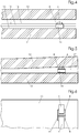
- Fig. 4 shows a cross-section through an entire glass-glass solar module laminate according to the invention before lamination with an embedding material layer 16 over the entire module width, but shorter than the total length of the solar module with a slightly too thick bypass element 14, ie the height of the bypass element 14 with lying on
- the above-contacted cross connector 4 and one-sided solderable terminal surface 8 is larger than the actually predetermined by the thickness of the embedding material and normally desired gap height, for example equal to 1.3 mm.
- the bypass element 14 is inserted in two layers of an embedding material 15 which extends through both the module width and the module length 14. Between the front glass pane 12 and the rear glass pane 13, a further shortened position of the embedding material 16 is arranged.
- FIG. 5 shows a cross section through a glass-glass solar module laminate after lamination with an embedding material layer 16 over the entire module width but shorter than the total length of the solar module, it can be seen that the back glass pane 13 and the front glass pane 12 are no longer accurate after lamination lie parallel to each other.
- the embedding material 17 after lamination in a bypass element with increased thickness is distributed over the module surface differently thick.
- a kind of slight waviness of the front glass pane 12 which follows the different gap heights at the points with intermediate bypass elements 14 and the intermediate surfaces with a small thickness between the spaced bypass elements 14.
- Fig. 6 shows a plan view of an embodiment and possible arrangement of a set between front glass pane 12 and rear glass pane 13 bypass element 14 according to FIG. 4 , From this it is apparent where, in particular, a bypass element 14 with solder surfaces 1 to be soldered on one side and the soldered transverse connectors 4 in relation to the module edge is approximately inserted.
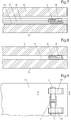
- Fig. 7 shows the arrangement of a novel spacer 18 for fixing the cross connector 4 after placing on a back glass pane 13 before lamination, embedded and enclosed by three layers of embedding material 15. This makes it possible all cross connector or connecting lines before and during the laminating reliable and immovable position.
- Fig. 8 shows a novel spacer 18 after laminating adjacent to the front glass pane 12 and the rear glass pane 13.
- the height of the spacer 18, which includes the cross connector 4 is less than or equal to the desired gap height wipe the two glass sheets 12, 13 after the lamination process and corresponds ideally, also the thickness of the potting material 19 after the completed lamination process.
- the spacers thus serve in addition to the reliable positioning of the cross connector 4 and the formation of a uniform gap height and a constant as possible parallelism of the front glass plate 12 and the back glass plate thirteenth
- Fig. 9 shows a plan view FIG. 4 and FIG. 6 . From the overview, the arrangement of a bypass element 14, the interconnected therewith cross-connector 4 and the position and arrangement of the spacer elements 18 can be seen. It is logical that the cross connector 4 can also be repeatedly arranged at certain intervals.
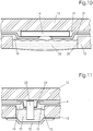
- Fig. 10 shows a slightly too thick bypass element 14 and its arrangement in an additionally introduced recess or opening 20 in the rear glass pane 13.
- the slightly too thick (ie more than 1.3 mm in height) by-pass element 14 is formed with one-sided solderable pads 8. With these pads 8 flat solderable cranked cross connector 21 are connected in the region of additionally introduced through the rear glass pane 13 opening 20.
- This composite of the cross connector 21 with the slightly too thick bypass element 14 is firmly embedded in the embedding material 19 after the lamination process.
- the additionally introduced into the rear glass pane 13 opening 20 is sealed with a suitable weather and climatic resistant material.
- the ends of the flat solderable cranked cross connector 21, which are connected to the bypass elements compensate for possible thermally different expansions occurring due to the offset and also serve for the eventual reduction of introduced mechanical stresses.
- Fig. 11 shows a considerably thicker bypass element 23 and its arrangement in an additionally introduced opening 20 in the rear glass pane 13.
- the flat cross connector 4 are here connected to the solderable bent connection pins of the bypass element 23.
- This also makes it possible, if necessary, to use considerably thicker bypass elements 23 which, because of their size, can even project beyond the rear outer surface of the rear glass pane 13 due to the additionally introduced opening 20.
- the free space between the embedding material 19 in the region of the opening 20, including the bypass element 23, is cast or encapsulated with a suitable filling material 22.
- a further cap 25 is arranged and glued.
- two transverse connector lines are arranged per solar module.
- three bypass elements are preferably arranged distributed and interconnected, wherein in two corners relatively far outside then two junction boxes with the corresponding module connection cables are arranged.
- the cross connectors are arranged at the edge of the module and have at each end a contact point with which the junction boxes are connected. Both junction boxes can be made relatively small and are located close to opposite module edges. These preferably contain no bypass elements.
- the bypass elements in the axis of the cross connectors are thermally far apart. Their heat loss is well dissipated along the cross connectors, as well as through their complete embedding between the two glass panes. The length of all lines, both between the inner module connection points and between adjacent solar modules of a row in series connection of the solar modules can be largely minimized by the inventive solution.
- a further advantage is that, depending on the application, it is possible to send thick bypass elements, such as monolithic or even hybrid low-voltage semiconductor diode elements, with pads on only one side on different sides or opposite sides, with or without terminal pins to be able to use.
- the number of connection surfaces may also be greater than two.
- connection of the bypass elements with other connecting elements is preferably carried out by welding, soldering, gluing or clamping.
- connection of bypass elements with the flat cross connectors is preferably carried out by soldering.
- bypass elements In the area of the bypass elements, additional embedding material for thickness compensation can optionally be added during lamination if the bypass elements used are too thick to reliably prevent glass breakage or blistering.
- the opening in the back glass pane for somewhat thicker bypass elements may be in the form of a circle, an ellipse, a long hole, a rectangle, or a combination of these shapes.
- the opening 20 in the rear glass pane 13, which is not completely filled by the bypass element, can be provided with filling material 22 and / or an additional suitable filling body before or after lamination.
- Their cover has the shape of a cap whose cap edge is formed circumferentially closed and is in a same plane.
- the cover is preferably made of weather-resistant material, such as metal, plastic, glass or ceramic.
Landscapes
- Photovoltaic Devices (AREA)
Description
- Die Erfindung betrifft eine Bypassanordnung in einem Glas-Glas-Solarmodul-Laminat mit innen liegenden Solarzellen mit oder ohne Rahmen.
- Solarmodul-Laminate bestehen aus einer Frontglasscheibe und einer Rückseitenfolie oder aus einer Frontglasscheibe und einer Rückglasscheibe, zwischen denen sich die aktiven Solarzellen, die elektrische Verbindungen und das Einbettungsmaterial befinden. Das Einbettungsmaterial wird vor dem Laminieren meist in der Form von zwei Folien (zwei Lagen) zugeführt und beigelegt, wobei die Abmessungen mit den Abmessungen der beiden Glasscheiben übereinstimmen. Die Lagen werden in der Regel hinter und vor den Solarzellen und den elektrischen Verbindungselementen angeordnet. Die Zellen sind elektrisch in der Regel in Reihe geschalten, wobei die beiden Enden der Reihenschaltung aller Zellen außen an gegenüberliegenden Modulkanten angeordnet sind und die inneren Modulanschlüsse darstellen. Diese inneren Modulanschlüsse sind meist durch relativ lange innere Verbindungsleitungen bis in die Nähe der Modulmitte geführt und durch die Rückseitenfolie bei Glas-Folien-Solarmodulen oder Rückglasscheibe hindurch auf der Rückseite des Moduls in einer externen außen angeordneten zentralen Anschlussdose zusammengeführt. Innerhalb der Anschlussdose sind die üblicherweise relativ großen Bypasselemente, wie Halbleiterdioden mit radialen oder axialen Anschlüssen, oder kleinere monolithische oder hybride Halbleiterdioden-Ersatzschaltungen, teilweise mit zusätzlichen Kühlelementen zur besseren Wärmeableitung aus dem Bypasselement im Innenraum der Anschlussdose, untergebracht und elektrisch angeschlossen.
- Jedes Bypasselement ist elektrisch nur über einen bestimmten Teil der Reihenschaltung aller einzelnen Solarzellen geschaltet, in der Regel über je 20 Solarzellen eines Moduls bei sogenannten 60 Zellen-Modulen. Die Bypasselemente dienen dem Zweck, im Falle von teilweisen Verschattungen des Solarmoduls die abgegebene Modulleistung so hoch wie möglich zu halten, da sonnst im Extremfall, obwohl nur wenige Einzelzellen beschattet sind alle Zellen des Moduls keinen Strom erzeugen. Gleichzeitig sollen sie Überhitzungen zuverlässig vermeiden um die aktiven Solarzellen vor einer Zerstörung zu bewahren.
- Bei der Herstellung von Solarmodulen mit Rückseitenfolien ist es bekannt, dass sich das Material der Rückseitenfolie während des Laminierprozesses ab etwa 150 C beginnt plastisch zu verformen. Damit kann sich die Form der Rückseitenfolie der Kontur zwischen liegender Bypasselemente mit den angeschlossenen Querverbindern anpassen. Bei zu großen Gesamthöhen der Bypasselemente besteht jedoch das Risiko, dass sich die Rückseitenfolie nicht ausreichend weit verformt, so dass im Bereich der Bypasselemente größere Hohlräume ohne Einbettungsmaterial entstehen, die letztlich die Zuverlässigkeit dieser Module einschränken können.
Die elektrischen Verbindungen der Bypasselemente und der äußeren Modulanschlüsse in der Anschlussdose mit den jeweiligen elektrischen Kontaktpunkten in der Reihenschaltung aller Zellen, erfolgen über lange und ggf. zusätzliche Verbindungsleitungen durch die Rückseitenfolie oder Rückglasscheibe hindurch und erfordern daher mindestens 12 Kontakte innerhalb einer Anschlussdose pro Solarmodul. Diese Kontakte können wahlweise z.B. als Löt-, Schweiß- oder Klemmverbindungen ausgebildet sein.
Alle elektrischen Kontaktpunkte für die Bypasselemente liegen üblicherweise an einem Rand der Zellenmatrix, an dem zugleich flache Querverbinder angeordnet sind, mit denen alle Zellenverbinder jeder dort befindlichen Randzelle elektrisch parallel geschaltet sind. Die Anschlussdosen dienen der sicheren mechanischen Verankerung und dem Schutz gegen klimatische Einflüsse aller darin endenden elektrischen Verbindungsleitungen aus dem Modulinneren und der beiden Modulanschlussleitungen nach außen, sowie aller dazu notwendigen elektrischen Kontaktverbindungen. Das DokumentUS-A-2010/0147364 zeigt ein Solarmodul mit einer Frontglasscheibe und einer Rückglasscheibe und dazwischen liegenden Solarzellen und Bypassdioden. Die Anschlussdosen tragen insbesondere mit ihrer ausliegenden Bodenplatte, sowie dem notwendigen Befestigungsmaterial in dem Bereich, in dem diese auf dem Solarmodul angeordnet und befestigt sind, zur verstärkten Erwärmung der dort befindlichen aktiven Solarzellen bei, da an dieser Stelle die Rückseitenfläche nicht gekühlt werden kann. Bypasselemente entwickeln zudem auch eigene zusätzliche Verlustwärme, die spätestens bei vollständiger Verschattung einer einzigen Zelle einen Maximalwert erreicht. Diese Verlustwärme trägt infolge Wärmestau insbesondere zur Erwärmung der gesamten Anschlussdose bei, da eine Belüftung der Anschlussdose zur Wärmeabfuhr aus Gründen des klimatischen Schutzes und aus Kostengründen nicht möglich ist. Durch diesen Wärmestau erhitzen sich die angeordneten Bypasselemente sehr stark, insbesondere das jeweils in der Mitte angeordnete, der drei notwendigen Bypasselemente, was ein gewisses Überhitzungsrisiko darstellt. - Solarzellen weisen bekannterweise einen negativen Temperaturkoeffizienten auf, d.h. der Wirkungsgrad der Umwandlung von Sonnenlicht in elektrische Energie sinkt mit wachsender Temperatur. In den meisten Anwendungsfällen werden Solarmodule im Solarmodulverbund angeordnet und genutzt, d. h. die Solarmodule sind ziemlich dicht nebeneinander in Zeilen und Spalten angeordnet. In der Regel werden die Modulanschlüsse vieler in der gleichen Zeile angeordneter Module elektrisch in Reihe untereinander verschaltet. Die notwendige Leitungslänge zwischen zentralen Anschlussdosen benachbarter Module beträgt damit immer etwas mehr als eine Solarmodulbreite.
- Dieser Aufbau und die Anordnung der Bypässe und deren wie vorstehend beschriebene Verschaltung führen zu folgenden Nachteilen:
- relativ lange, und ggf. zusätzliche Verbindungsleitungen zwischen Bypasselementen und Anschlussdose (erhöhter Aufwand und größere elektrische Verluste)
- relativ lange Verbindungsleitungen der inneren Modulanschlüsse vom Modulrand bis in Nähe der Modulmitte zur tatsächlichen Position der Anschlussdose (erhöhter Aufwand, größere elektrische Verluste)
- hohe Kontaktanzahl von mindestens 12 Kontaktverbindungen pro Modul innerhalb einer Anschlussdose zur Verbindung der Bypasselemente, sowie der inneren und äußeren Modulanschlüsse notwendig (Zuverlässigkeitsrisiko der Kontakte, erhöhter Aufwand)
- die Leitungslänge zwischen zentral angeordneten Anschlussdosen benachbarter Module beträgt mindestens etwas mehr als die Modulbreite und ist damit relativ groß (dies bedingt einen erhöhter Aufwand und größere elektrische Verluste)
- Anschlussdosen mit großen Abmessungen erforderlich, verursacht durch viele Kontaktverbindungen sowie die drei Bypasselemente, dies führt zur Verschlechterung des Modulwirkungsgrades infolge Wärmeisolation und Eigenerwärmung mit Wärmestau
- Überhitzungsrisiko der Bypasselemente infolge Wärmestau innerhalb Anschlussdose
- Vorgefertigte relativ lange Stränge von Bypasselementen und Querverbindern, diese sind biegeempfindlich und schwierig zu handhaben
- Der Erfindung liegt die Aufgabe zu Grunde ein Solarmodul-Laminat zu schaffen, bei dem die Länge der Verbindungsleitungen zwischen den Bypasselementen und der Anschlussdose reduziert wird, relativ lange Verbindungsleitungen der inneren Modulanschlüsse vom Modulrand bis in die Nähe der Modulmitte zur Anschlussdose hin vermieden werden, die Kontaktanzahl pro Modul innerhalb Anschlussdose zur Verbindung der Bypasselemente sowie der inneren und äußeren Modulanschlüsse reduziert wir, die Leitungslänge zwischen den Anschlussdosen benachbarter im Verbund verlegter Solarmodule weiter verringert wird und sich der Modulwirkungsgrad und die Lebensdauer weiter erhöht.
- Die Aufgabe der Erfindung wird mit den Merkmalen des Hauptanspruches gelöst. Weitere vorteilhafte Ausgestaltungen sind Gegenstand der rückbezüglichen Unteransprüche. Erfindungsgemäß können bei der neuartigen Bypassanordnung in einem Glas-Glas-Solarmodul-Laminat mit innen liegenden Solarzellen, d. h. eingebetteten Solarzellen, mit mehreren kontaktierten Schaltelementen mit oder ohne Rahmen und mit üblichen Anschlussleitungen und Anschlussdosen, zwischen einer Frontglasscheibe 12 und einer Rückglasscheibe 13 in Abhängigkeit von ihrer Dicke mehrere Bypasselemente 1, 6, 14 oder 23 mit unterschiedlicher Höhe angeordnet werden. Bei Bypasselementen die eine größere Dicke als 1,3 mm besitzen, wie beispielsweise bei den dicker als 1,3 mm ausgebildeten Bypasselementen 14 oder 23 sind im Rückseitenglas 13 zusätzliche Aussparungen oder Öffnungen 20 angeordnet. Die Öffnungen 20 können zum Beispiel mittels geeigneter Bohrverfahren hergestellt werden. Die Aussparungen 20 können je nach Bedarf auch eingeätzt oder eingefräst ausgebildet werden. In diesen Öffnungen oder Aussparungen 20 sind dann vorrangig die zu dicken Bypasselemente 14 oder 23 positioniert und mit den entsprechenden Querverbindern 4 kontaktiert. Dabei sind die Bypasselemente 1, 6, 14 oder 23 jeweils in der Längsachse derjenigen zwei Querverbinder 4, 5 oder 21 angeordnet und positioniert, die ihren elektrischen Kontaktpunkten entsprechen und es sind wenigstens zwei Anschlussdosen außen an den Modulrändern angeordnet.
- Bei einer besonderen vorteilhaften Ausführung des Glas-Glas-Solarmodul-Laminats sind die Dicken der verschalteten Bypasselemente kleiner gleich 1,3 mm. Dies führt zu einer besonders flachen Bauweise solch eines Glas-Glas-Solarmodul-Laminats. In einer speziellen Ausführung ist der Zwischenraum zwischen der Frontglasscheibe 12 und der Rückglasscheibe 13 bei einem solchen Glas-Glas-Solarmodul-Laminat kleiner gleich 1mm.
- In einer anderen Ausführung des erfindungsgemäßen Glas-Glas-Solarmodul-Laminats sind die zusätzlichen Aussparungen 20 nur Innen in der Rückglasscheibe 13 oder nur in Innen in der Frontglasscheibe 12 oder sowohl in der Frontglasscheibe 12 als auch in der Rückglasscheibe 13 als flächige, beliebig geformte, nicht nach außen durchgehende Aussparungen ausgebildet. In diesen Aussparungen sind dann die verbundenen Bypasselemente 14 eingelegt und positioniert. Diese Ausführung ist zwar in der Herstellung etwas aufwändiger, da an den entsprechenden Stellen in der Frontglasscheibe 12 oder in der Rückglasscheibe 13 oder in beiden Scheiben 21, 13 die Aussparungen mit geeigneten Verfahren einzubringen sind. Da diese Art von Aussparungen nicht als durchgehende Öffnungen ausgebildet sind, bleib das gesamte Solarmodul dauerhaft gekapselt und als ganzes nach dem Laminierprozess dicht gegenüber irgendwelchen von außen einwirkenden Umwelteinflüssen.
- Von Vorteil ist es Weiterhin wenn zwischen der Frontglasscheibe 12 und der Rückglasscheibe 13 Abstandshalter angeordnet und positioniert sind, deren Dicke kleiner gleich dem Abstand zwischen der Frontglasscheibe 12 und der Rückglasscheibe 13 ist.
- Beim neuartigen Verfahren zur Herstellung eines Glas-Glas-Solarmodul-Laminats werden die Solarzellen auf das, mit mindestens einer Lage Einbettungsmaterial 15 und/odere 16 versehene Frontglasscheibe 12 oder das mit mindestens einer Lage Einbettungsmaterial 15 und/oder 16 versehnen Rückglasscheibe 13 aufgelegt und positioniert. Anschließend werden die jeweils einzusetzenden Bypasselemente 1, 6, 14 oder 23 und je nach Bedarf die zugehörigen Querverbinder 4, 5 oder 21 einzeln oder teilweise in vorgefertigten Teilsträngen aufgelegt und positioniert. Bevorzugt sind dabei die Querverbinder 4, 5 oder 21 mit zusätzlich beigelegten Abstandshaltern 18 in ihrer Lage genau positioniert. Im Anschluss erfolgt dann das Kontaktieren aller Bauteile untereinander. In der Regel erfolgt das Kontaktieren mittels geeigneter Lötprozesse. Die Abstandshalter können wahlweise gegebenenfalls auch wieder entfern werden. Dann werden ein, zwei oder mehrere Lagen Einbettungsmaterial 15 bzw. 16 aufgelegt. Nunmehr kann die noch fehlende Rückglasscheibe 13, oder das je nach Art des gewählten Fertigungsverfahrens, die Frontglasscheibe 12 aufgelegt werden. Zum Schluss erfolg dann das Laminieren nach einem der bekannten, in der Branche üblichen, Laminierprozesse.
- Durch die erfindungsgemäße Bypassanordnung und das neuartige Verfahren zur Herstellung des Glas-Glas-Solarmodul-Laminat wird es möglich die Länge der Verbindungsleitungen zwischen den Bypasselementen und der Anschlussdose erheblich zu reduzieren. Es gelingt die bislang relativ langen Verbindungsleitungen der inneren Modulanschlüsse vom Modulrand bis in die Nähe der Modulmitte zur Anschlussdose hin zu vermeiden. Des Weitern wird die Kontaktanzahl pro Modul innerhalb jeder Anschlussdose zur Verbindung der Bypasselemente sowie der inneren und äußeren Modulanschlüsse verringert. Insgesamt kann auch die Leitungslänge zwischen den Anschlussdosen benachbarter im Verbund verlegter Solarmodule erheblich weiter verringert werden. Durch die technische Lösung kann ebenfalls der Modulwirkungsgrad gesteigert und die Lebensdauer weiter erhöht werden. Zudem sinkt das Risiko, dass sich einzelne Solarzellen oder ganze Bereiche innerhalb des neuartigen Glas-Glas-Solarmodul-Laminats überhitzen und damit für immer bei der Energieerzeugung ausfallen, d. h. die Modullebensdauer wird verbessert.
- Weitere Einzelheiten, Merkmale und Vorteile der Erfindung ergeben sich aus der nachfolgenden Beschreibung von Ausführungsbeispielen mit Bezugnahme auf die zugehörigen Zeichnungen. Es zeigen:
- Fig. 1
- zeigt ein Bypasselement 1 als ein Halbleiter-Diodenchip mit einem aufliegenden flachen lötfähigen Querverbinder 5 und einem unteren normalen lötfähigen Querverbinder 4
- Fig. 2
- zeigt ein Bypasselement 6 als eine Dioden-Ersatzschaltung mit Kunststoffkapselung mit seitlich herausgeführten abgestuften Anschlussflächen 7 mit aufliegenden normal flachen lötfähigen Querverbindern 4
- Fig. 3
- zeigt ein Bypasselement als eine Dioden-Ersatzschaltung mit Kunststoffkapselung mit nebenliegenden Querverbindern 4 und biegsamen lötfähigen Anschlussfahnen 9
- Fig. 4
- zeigt einen Querschnitt durch ein Glas-Glas-Solarmodul-Laminat vor dem Laminieren mit einer Einbettungsmateriallage 16 über die gesamte Modulbreite aber kürzer ausgeführt als die Gesamtlänge des Solarmoduls
- Fig. 5
- zeigt einen Querschnitt durch ein Glas-Glas-Solarmodul-Laminat nach dem Laminieren mit einer Einbettungsmateriallage 16 über die gesamte Modulbreite aber kürzer ausgeführt als die Gesamtlänge des Solarmoduls
- Fig. 6
- zeigt eine Draufsicht auf eine Ausführung gemäß
Figur 4 - Fig. 7
- zeigt einen neuartigen Abstandshalter 18 vor dem Laminieren eingebettet und umschlossen von Einbettungsmaterial 15
- Fig. 8
- zeigt einen neuartigen Abstandshalter 18 nach dem Laminieren anliegend an der Frontglasscheibe 12 und der Rückglasscheibe 13
- Fig. 9
- zeigt eine Draufsicht nach
Figur 4 und Figur 6 - Fig. 10
- zeigt ein geringfügig zu dickes Bypasselement 14 und dessen Anordnung in einer zusätzlich eingebrachten Öffnung 20 in der Rückglasscheibe 20
- Fig. 11
- zeigt ein dickeres Bypasselement 23 und dessen Anordnung in einer zusätzlich eingebrachten Aussparung oder Öffnung 20 in der Rückglasscheibe 13
-
Fig. 1 zeigt im Querschnitt ein sehr dünnes flaches Bypasselement (einen Halbleiter-Diodenchip) 1 mit einer oberen Anschlussfläche 2 auf dem Diodenchip und einer unteren Anschlussfläche 3 unter dem Diodenchip. Die obere Anschlussfläche 2 ist mit einem aufliegenden besonders flachen lötfähigen Querverbinder 5 und die untere Anschlussfläche 3 ist mit einem normalen lötfähigen üblichen Querverbinder 4 kontaktiert. Dieses sehr flach bauende verschaltete Bypasselement 1 ist zwischen einer durchgehend gleichmäßig dick ausgebildeten Frontglasscheibe 1 und Rückglasscheibe 2 einlaminiert (zeichnerisch nicht dargestellt). -
Fig. 2 zeigt eine ähnliche Anordnung mit einem dünnen Bypasselement 6, welches als eine Dioden-Ersatzschaltung mit zusätzlicher Kunststoffkapselung ausgeführt ist. Hier sind die Anschlussfahnen 7, seitlich abgestuft ausgeführt auf denen die üblichen normal flachen Querverbinder 7 kontaktiert sind Diese Anordnung kann ebenfalls noch zwischen einer durchgehend gleichmäßig dick ausgebildeten Frontglasscheibe 1 und gleichartiger Rückglasscheibe 2 einlaminiert werden (zeichnerisch nicht dargestellt). -
Fig. 3 zeigt dünnes Bypasselement 6 als eine Dioden-Ersatzschaltung ebenfalls mit umhüllender Kunststoffkapselung aber anderer Anschlussart. Die Querverbinder 4 mit der Lötverbindung 11 des Querverbinders sind hier seitlich beabstandet ausgeführt und werden mittels besonders flachen und zugleich biegsamen Anschlussfahnen 9 auf der Oberseite des Bypasselements 6 mit der Lötverbindung des Bypasselement 10 kontaktiert, dessen Anschlussflächen 8 einseitig lötfähig ausgebildet und angeordnet sind. Die Kontakte (zwei einseitig lötfähige Anschlussflächen 8) des Bypasselements 6 sind hier voneinander getrennt nur auf einer Seite durch die Kunststoffkapselung nach außen geführt. -
Fig. 4 zeigt einen Querschnitt durch ein gesamtes erfindungsgemäßes Glas-Glas-Solarmodul-Laminat vor dem Laminieren mit einer Einbettungsmateriallage 16 über die gesamte Modulbreite, aber kürzer ausgeführt als die Gesamtlänge des Solarmoduls mit einem geringfügig zu dicken Bypasselement 14, d. h. die Höhe des Bypasselements 14 mit aufliegendem oben kontaktierten Querverbinder 4 und einseitig lötfähiger Anschlussfläche 8 ist größer als die eigentlich durch die Dicke des Einbettungsmaterials vorgegebene und normalerweise gewünschte Spalthöhe zum Beispiel gleich 1,3 mm. Das Bypasselement 14 ist hier in diesem Beispiel in zwei Lagen eines sowohl über die Modulbreite als auch über die Modullänge 14 durchgehenden Einbettungsmaterials 15 eingelegt. Zwischen der Frontglasscheibe 12 und der Rückglasscheibe 13 ist eine weitere verkürzte Lage des Einbettungsmaterials 16 angeordnet. - Dies bewirkt, wie aus
Figur 5 , welche einen Querschnitt durch ein Glas-Glas-Solarmodul-Laminat nach dem Laminieren mit einer Einbettungsmateriallage 16 über die gesamte Modulbreite aber kürzer ausgeführt als die Gesamtlänge des Solarmoduls zeigt, ersichtlich, dass die Rückglasscheibe 13 und die Frontglasscheibe 12 nach dem Laminieren nicht mehr genau parallel zueinander liegen. Das Einbettungsmaterial 17 nach dem Laminieren bei einem Bypasselement mit erhöhter Dicke ist über die Modulfläche verteilt unterschiedlich dick. Letztlich entsteht hier eine Art leichte Welligkeit der Frontglasscheibe 12, welche den die unterschiedliche Spalthöhen an der Stellen mit zwischen liegenden Bypasselementen 14 und den Zwischenflächen mit geringer Dicke zwischen den beabstandeten Bypasselementen 14 folgt. -
Fig. 6 zeigt eine Draufsicht auf eine Ausführung und mögliche Anordnung eines zwischen Fronglasscheibe 12 und Rückglasscheibe 13 gelegten Bypasselements 14 gemäßFigur 4 . Hieraus wird ersichtlich, wo insbesondere ein Bypasselement 14 mit einseitig lötfähigen Anschlussflächen 8 und den aufgelöteten Querverbindern 4 im Bezug zum Modulrand in etwa eingelegt ist. -
Fig. 7 zeigt die Anordnung eines neuartigen Abstandshalters 18 zur Fixierung der Querverbinder 4 nach dem Auflegen auf eine Rückglasscheibe 13 vor dem Laminieren, eingebettet und umschlossen von drei Lagen Einbettungsmaterial 15. Dadurch wird es möglich alle Querverbinder bzw. Verbindungsleitungen vor und während des Laminierprozesses zuverlässig und unverrückbar zu positionieren. -
Fig. 8 zeigt einen neuartigen Abstandshalter 18 nach dem Laminieren anliegend an der Frontglasscheibe 12 und der Rückglasscheibe 13. Die Höhe des Abstandshalters 18, der den Querverbinder 4 umfasst, ist dabei jeweils kleiner gleich der gewünschten Spalthöhe wischen den beiden Glasscheiben 12, 13 nach dem Laminierprozess und entspricht idealerweise auch der Dicke des Einbettungsmaterials 19 nach dem abgeschlossenen Laminierprozess. Die Abstandshalter dienen also neben der zuverlässigen Positionierung der Querverbinder 4 auch der Ausbildung einer gleichmäßigen Spalthöhe und einem möglichst gleichbleibenden Parallelität der Frontglasplatte 12 und der Rückglasplatte 13. -
Fig. 9 zeigt eine Draufsicht nachFigur 4 und Figur 6 , aus der überblicksmäßig die Anordnung eines Bypasselements 14, die damit verschalteten Querverbinder 4 und die Lage und Anordnung der Abstandselemente 18 ersichtlich ist. Es ist logisch, dass die Querverbinder 4 in gewissen Abständen auch mehrfach wiederholt angeordnet sein können. -
Fig. 10 zeigt ein geringfügig zu dickes Bypasselement 14 und dessen Anordnung in einer zusätzlich eingebrachten Aussparung oder Öffnung 20 in der Rückglasscheibe 13. Das geringfügig zu dicke (d. h. in der Höhe mehr als 1,3 mm) Bypasselement 14 ist mit einseitig lötfähigen Anschlussflächen 8 ausgebildet. Mit diesen Anschlussflächen 8 sind im Bereich der zusätzlich durch die Rückglasscheibe 13 hindurch eingebrachten Öffnung 20 flache lötfähige abgekröpfte Querverbinder 21 verbunden. Dieser Verbund der Querverbinder 21 mit dem geringfügig zu dicken Bypasselement 14 ist in das Einbettungsmaterial 19 nach erfolgtem Laminierprozess fest eingebettet. Die zusätzlich in die Rückglasscheibe 13 eingebrachte Öffnung 20 ist mit einem geeigneten Witterungs- und Klimabeständigen Material dicht verschlossen. Die Enden der flachen lötfähigen abgekröpften Querverbinder 21, die mit den Bypasselementen verbunden sind, kompensieren durch die Kröpfung auftretende möglich thermisch unterschiedliche Ausdehnungen und dienen auch zum eventuellen Abbau eingebrachter mechanischer Spannungen. -
Fig. 11 zeigt ein erheblich dickeres Bypasselement 23 und dessen Anordnung in einer zusätzlich eingebrachten Öffnung 20 in der Rückglasscheibe 13. Die flachen Querverbinder 4 sind hier mit den lötfähigen abgekröpften Anschlusspins des Bypasselements 23 verbunden. Dadurch ist es auch möglich bei Bedarf erheblich dickere Bypasselemente 23 einzusetzen, die wegen ihrer Größe sogar durch die zusätzlich eingebrachte Öffnung 20 über die rückseitige Außenfläche der Rückglasscheibe 13 hinausragen können. Der freie Zwischenraum zwischen Einbettungsmaterial 19 im Bereich der Öffnung 20 einschließlich das Bypasselement 23 sind mit einem geeigneten Füllmaterial 22 aus bzw. umgossen. Zusätzlich ist es vorteilhaft, wenn wegen einer höheren Dichtheit eine weitere Abdeckkappe 25 angeordnet und aufgeklebt ist. - In der Regel sind pro Solarmodul zwei Querverbinderleitungen angeordnet in den Querverbindern sind bevorzugt drei Bypasselemente verteilt angeordnet und verschaltet, wobei in zwei Ecken relativ weit außen dann zwei Anschlussdosen mit den entsprechenden Modulanschlusskabeln angeordnet sind. Die Querverbinder sind am Rand des Moduls angeordnet und weisen an jedem Ende einen Kontaktpunkt auf mit dem die Anschlussdosen verbunden sind. Beide Anschlussdosen können relativ klein ausgebildet werden und sind nahe an gegenüberliegenden Modulkanten angeordnet. Diese enthalten bevorzugt keine Bypasselemente. Die Bypasselemente in der Achse der Querverbinder sind thermisch weit voneinander entfernt angeordnet. Ihre Verlustwärme wird entlang der Querverbinder, sowie durch ihre vollständige Einbettung zwischen den beiden Glasscheiben gut abgeleitet. Die Länge aller Leitungen sowohl zwischen den inneren Modulanschlusspunkten als auch zwischen benachbarten Solarmodulen einer Zeile bei Reihenschaltung der Solarmodule kann durch die erfindungsgemäße Lösung weitgehend minimiert werden.
- Ein weiterer Vorteil besteht darin, dass es je nach Einsatzfall möglich ist, verschicken Dicke Bypasselemente wie zum Beispiel monolithische oder auch hybride Halbleiter-Dioden-Element mit geringer Flußspannung, mit Anschlussflächen auf nur einer Seite auf verschiedenen Seiten oder gegenüberliegenden Seiten, mit oder ohne Anschlusspins einsetzen zu können. Pro Bypasselement kann die Anzahl der Anschlussflächen auch gegebenenfalls größer als zwei sein.
- Die Verbindung der Bypasselemente mit anderen Verbindungselementen erfolgt bevorzugt durch Schweißen, Löten, Kleben oder Klemmen.
- Die Verbindung von Bypasselementen mit den flachen Querverbindern erfolgt vorzugsweise durch Löten.
- Im Bereich der Bypasselemente kann wahlweise beim Laminieren zusätzliches Einbettungsmaterial zum Dickenausgleich beigefügt werden, falls die eingesetzten Bypasselemente zu dick sind, um Glasbrüche oder Blasenbildung zuverlässig zu vermeiden. Die Öffnung in der Rückglasscheibe für etwas dickere Bypasselemente kann die Form eines Kreises, einer Ellipse, eines Langlochs, Rechtecks oder eine Kombinationen dieser Formen haben.
- Die durch das Bypasselement nicht vollständig ausgefüllte Öffnung 20 in der Rückglasscheibe 13 kann vor oder nach dem Laminieren mit Füllmaterial 22 und/oder einem zusätzlichen geeigneten Füllkörper versehen werden.
- Deren Abdeckung weist die Form einer Abdeckkappe auf, deren Kappenrand umlaufend geschlossen ausgebildet ist und sich in einer gleichen Ebene befindet. Die Abdeckung besteht bevorzugt aus wetterbeständigem Material, z.B. Metall, Kunststoff, Glas oder Keramik.
-
- 1
- flaches Bypasselement (Halbleiter-Diodenchip)
- 2
- obere Anschlussfläche am Diodenchip
- 3
- untere Anschlussfläche am Diodenchip
- 4
- lötfähiger Querverbinder flach,
- 5
- flacher lötfähiger Querverbinder mit abgeflachte Anschlussfahne
- 6
- Bypasselement als Dioden-Ersatzschaltung mit Kunststoffkapselung
- 7
- seitlich herausgeführte, abgestufte Anschlussfläche
- 8
- einseitige lötfähige Anschlussflächen
- 9
- biegsame Anschlussfahne (dünner als Querverbinder)
- 10
- Lötverbindung zum Bypasselement
- 11
- Lötverbindung zum Querverbinder
- 12
- Frontglasscheibe
- 13
- Rückglasscheibe
- 14
- geringfügig zu dickes Bypasselement
- 15
- Einbettungsmateriallage über gesamte Modulfläche
- 16
- Einbettungsmateriallage über gesamte Modulbreite, kürzer als Gesamtlänge
- 17
- Einbettungsmaterial nach Laminieren bei einem Bypasselement mit erhöhter Dicke
- 18
- Abstandshalter
- 19
- Einbettungsmaterial nach abgeschlossenen Laminierprozess
- 20
- Aussparungen oder Öffnungen in der Rückglasscheibe
- 21
- flacher lötfähiger abgekröpfter Querverbinder
- 22
- Füllmaterial
- 23
- dickes Bypasselement
- 24
- lötfähiges, abgekröpftes Anschlusspin
- 25
- Abdeckkappe
Claims (4)
- Glas-Glas-Solarmodul-Laminat mit innenliegenden Solarzellen, wobei zwischen einer Frontglasscheibe (12) und einer Rückglasscheibe (13) Bypasselemente (1, 6, 14, 23) mit gleicher oder unterschiedlicher Höhe angeordnet sind, weiterhin die Bypasselemente (1, 6, 14, 23) Querverbinder (4, 5, 7) aufweisen, welche mit Anschlussflächen (2, 3) eines Diodenchip (1) kontaktiert sind, und mit wenigstens zwei, am Modulrand angeordneten Anschlussdosen,
dadurch gekennzeichnet, dass
Abstandshalter (18) vorgesehen sind, welche den jeweiligen Querverbinder (4) umfassen, wobei die Höhe des Abstandshalters (18) gleich oder kleiner als die Spaltbreite zwischen der Frontglas- und der Rückglasscheibe (12; 13) nach dem Laminierprozess ist, wobei die Abstandshalter(18) sowohl der Positionierung der Querverbinder (4) als auch der Ausbildung einer gleichmäßigen Spalthöhe und möglichst gleichbleibender Parallelität zwischen der Frontglasscheibe (12) und der Rückglasscheibe (13) dienen. - Glas-Glas-Solarmodul-Laminat nach Anspruch 1,
dadurch gekennzeichnet, dass
bei einer Dicke der Bypasselemente (14, 23) von größer 1,3 mm in der Rückglasscheibe (13) zusätzliche Aussparungen oder Öffnungen (20) angeordnet sind, in denen die zu dicken Bypasselemente (14, 23) angeordnet und kontaktiert sind. - Glas-Glas-Solarmodul-Laminat nach Anspruch 2,
dadurch gekennzeichnet, dass
zusätzliche Aussparungen (20) nur an der Innenseite der Rückglasscheibe (13) als nicht nach außen durchgehende Aussparungen ausgebildet sind. - Glas-Glas-Solarmodul-Laminat nach Anspruch 2 oder 3,
dadurch gekennzeichnet, dass
weitere Aussparungen (20) an der Innenseite der Frontglasscheibe (12) als flächige, beliebig geformte, nicht nach außen durchgehende Aussparungen (20) ausgebildet sind.
Applications Claiming Priority (2)
| Application Number | Priority Date | Filing Date | Title |
|---|---|---|---|
| DE102013104109 | 2013-04-23 | ||
| DE102014105598.5A DE102014105598A1 (de) | 2013-04-23 | 2014-04-17 | Bypassanordnung in einem Glas-Glas-Solarmodul-Laminat mit Solarzellen |
Publications (2)
| Publication Number | Publication Date |
|---|---|
| EP2797121A1 EP2797121A1 (de) | 2014-10-29 |
| EP2797121B1 true EP2797121B1 (de) | 2017-12-13 |
Family
ID=50976567
Family Applications (1)
| Application Number | Title | Priority Date | Filing Date |
|---|---|---|---|
| EP14401047.7A Not-in-force EP2797121B1 (de) | 2013-04-23 | 2014-04-22 | Bypassanordnung in einem Glas-Glas-Solarmodul-Laminat mit Solarzellen |
Country Status (3)
| Country | Link |
|---|---|
| EP (1) | EP2797121B1 (de) |
| DE (1) | DE102014105598A1 (de) |
| ES (1) | ES2658229T3 (de) |
Cited By (1)
| Publication number | Priority date | Publication date | Assignee | Title |
|---|---|---|---|---|
| DE102018120248A1 (de) * | 2018-08-20 | 2020-02-20 | EnBW Energie Baden-Württemberg AG | Verfahren zur Verschaltung von Solarzellen, dazugehöriger Solarzellenstring sowie dazugehöriges Solarmodul |
Families Citing this family (3)
| Publication number | Priority date | Publication date | Assignee | Title |
|---|---|---|---|---|
| DE102016115440B4 (de) * | 2016-08-19 | 2022-07-14 | Hanwha Q Cells Gmbh | Dioden-Kontaktierung für ein Solarmodul und ein Verfahren zur Kontaktierung einer Diode für ein Solarmodul |
| WO2025073501A1 (de) | 2023-10-02 | 2025-04-10 | Saint-Gobain Sekurit France | Verbundscheibe mit photovoltaikmodul |
| DE102024106441A1 (de) * | 2024-03-06 | 2025-09-11 | Weidmüller Interface GmbH & Co. KG | Bypass-Element und Photovoltaikmodul mit mindestens einem Bypass- Element |
Family Cites Families (2)
| Publication number | Priority date | Publication date | Assignee | Title |
|---|---|---|---|---|
| WO2010077952A1 (en) * | 2008-12-16 | 2010-07-08 | Solopower, Inc. | Thin film photovoltaic module manufacturing methods and structures |
| US20130050227A1 (en) * | 2011-08-30 | 2013-02-28 | Qualcomm Mems Technologies, Inc. | Glass as a substrate material and a final package for mems and ic devices |
-
2014
- 2014-04-17 DE DE102014105598.5A patent/DE102014105598A1/de not_active Ceased
- 2014-04-22 ES ES14401047.7T patent/ES2658229T3/es active Active
- 2014-04-22 EP EP14401047.7A patent/EP2797121B1/de not_active Not-in-force
Non-Patent Citations (1)
| Title |
|---|
| None * |
Cited By (1)
| Publication number | Priority date | Publication date | Assignee | Title |
|---|---|---|---|---|
| DE102018120248A1 (de) * | 2018-08-20 | 2020-02-20 | EnBW Energie Baden-Württemberg AG | Verfahren zur Verschaltung von Solarzellen, dazugehöriger Solarzellenstring sowie dazugehöriges Solarmodul |
Also Published As
| Publication number | Publication date |
|---|---|
| DE102014105598A1 (de) | 2014-10-23 |
| ES2658229T3 (es) | 2018-03-08 |
| EP2797121A1 (de) | 2014-10-29 |
Similar Documents
| Publication | Publication Date | Title |
|---|---|---|
| DE69229030T2 (de) | Solarzellenmodul | |
| DE112016003768B4 (de) | Sonnenkollektor | |
| DE112014006676B4 (de) | Leistungsmodulvorrichtung | |
| DE102010016721B4 (de) | Elektronische Baueinheit | |
| DE2049093B2 (de) | Relaistraeger- und anschlussplatte fuer eine schaltanordnung | |
| EP3818574B1 (de) | Pouchzelle und stack | |
| EP2797121A1 (de) | Bypassanordnung in einem Glas-Glas-Solarmodul-Laminat mit Solarzellen | |
| DE102019134674A1 (de) | Halbleitervorrichtung und Verfahren zum Herstellen derselben | |
| WO2018041860A1 (de) | Verbindungsplatte für eine batterie und batterie | |
| WO2019092072A1 (de) | Modulgehäuse für ein stapelbares batteriemodul, batteriemodul sowie batteriestapel | |
| DE102006035626A1 (de) | Verfahren zum Anbringen eines Verbindungsleiters an einer photovoltaischen Solarzelle | |
| EP1220314B1 (de) | Leistungshalbleitermodul | |
| DE102015105326A1 (de) | Batterienzellenaufnahmemodul | |
| EP2728627B1 (de) | Verbindungseinrichtung und Anordnung hiermit und mit einem Photovoltaikmodul | |
| EP2475014A2 (de) | Photovoltaikmodul mit einlaminierter Bypassdiode | |
| DE19740570C2 (de) | Piezoelektrischer Aktor mit einem elektrischen Anschluß | |
| WO2022089947A1 (de) | Solarzellenmodul | |
| WO2014072038A1 (de) | Leiterplattenelement und zellenanordnung | |
| DE112015003463B4 (de) | Halbleiterbauelement, Beleuchtungsvorrichtung und Verfahren zur Herstellung eines Halbleiterbauelements | |
| DE102017214347A1 (de) | Verfahren zur Herstellung eines Fassadenelements sowie Fassadenelement | |
| DE102015218526B4 (de) | Anschlussanordnung für ein Solarmodul | |
| DE29915648U1 (de) | Solarziegel in Modulbauweise | |
| EP2549552A2 (de) | Solarzellenbaustein und Solarzellenanordnung | |
| DE1614134B2 (de) | Leiterrahmen zur Verwendung bei der automatischen Herstellung von gekapselten, integrierten Halbleiterbauelementen, integriertes Halbleiterbauelement und Verfahren zu dessen Herstellung | |
| DE102015111696A1 (de) | Solarmodul mit direkter Kontaktierung einer Bypass-Diode mit einem Querverbinder |
Legal Events
| Date | Code | Title | Description |
|---|---|---|---|
| PUAI | Public reference made under article 153(3) epc to a published international application that has entered the european phase |
Free format text: ORIGINAL CODE: 0009012 |
|
| 17P | Request for examination filed |
Effective date: 20140422 |
|
| AK | Designated contracting states |
Kind code of ref document: A1 Designated state(s): AL AT BE BG CH CY CZ DE DK EE ES FI FR GB GR HR HU IE IS IT LI LT LU LV MC MK MT NL NO PL PT RO RS SE SI SK SM TR |
|
| AX | Request for extension of the european patent |
Extension state: BA ME |
|
| R17P | Request for examination filed (corrected) |
Effective date: 20150415 |
|
| RIN1 | Information on inventor provided before grant (corrected) |
Inventor name: LIPPMANN, ROBERT Inventor name: UHLMANN, RUEDIGER Inventor name: KUENANZ, STEFFEN Inventor name: FRIEDRICH, STEFFEN |
|
| GRAP | Despatch of communication of intention to grant a patent |
Free format text: ORIGINAL CODE: EPIDOSNIGR1 |
|
| STAA | Information on the status of an ep patent application or granted ep patent |
Free format text: STATUS: GRANT OF PATENT IS INTENDED |
|
| INTG | Intention to grant announced |
Effective date: 20170728 |
|
| RAP1 | Party data changed (applicant data changed or rights of an application transferred) |
Owner name: SOLARWATT GMBH |
|
| GRAS | Grant fee paid |
Free format text: ORIGINAL CODE: EPIDOSNIGR3 |
|
| GRAA | (expected) grant |
Free format text: ORIGINAL CODE: 0009210 |
|
| STAA | Information on the status of an ep patent application or granted ep patent |
Free format text: STATUS: THE PATENT HAS BEEN GRANTED |
|
| REG | Reference to a national code |
Ref country code: GB Ref legal event code: FG4D Free format text: NOT ENGLISH |
|
| REG | Reference to a national code |
Ref country code: AT Ref legal event code: REF Ref document number: 955159 Country of ref document: AT Kind code of ref document: T Effective date: 20171215 Ref country code: CH Ref legal event code: EP |
|
| REG | Reference to a national code |
Ref country code: IE Ref legal event code: FG4D Free format text: LANGUAGE OF EP DOCUMENT: GERMAN |
|
| REG | Reference to a national code |
Ref country code: DE Ref legal event code: R096 Ref document number: 502014006550 Country of ref document: DE |
|
| REG | Reference to a national code |
Ref country code: ES Ref legal event code: FG2A Ref document number: 2658229 Country of ref document: ES Kind code of ref document: T3 Effective date: 20180308 |
|
| REG | Reference to a national code |
Ref country code: NL Ref legal event code: MP Effective date: 20171213 |
|
| PG25 | Lapsed in a contracting state [announced via postgrant information from national office to epo] |
Ref country code: FI Free format text: LAPSE BECAUSE OF FAILURE TO SUBMIT A TRANSLATION OF THE DESCRIPTION OR TO PAY THE FEE WITHIN THE PRESCRIBED TIME-LIMIT Effective date: 20171213 Ref country code: SE Free format text: LAPSE BECAUSE OF FAILURE TO SUBMIT A TRANSLATION OF THE DESCRIPTION OR TO PAY THE FEE WITHIN THE PRESCRIBED TIME-LIMIT Effective date: 20171213 Ref country code: NO Free format text: LAPSE BECAUSE OF FAILURE TO SUBMIT A TRANSLATION OF THE DESCRIPTION OR TO PAY THE FEE WITHIN THE PRESCRIBED TIME-LIMIT Effective date: 20180313 |
|
| PG25 | Lapsed in a contracting state [announced via postgrant information from national office to epo] |
Ref country code: LV Free format text: LAPSE BECAUSE OF FAILURE TO SUBMIT A TRANSLATION OF THE DESCRIPTION OR TO PAY THE FEE WITHIN THE PRESCRIBED TIME-LIMIT Effective date: 20171213 Ref country code: BG Free format text: LAPSE BECAUSE OF FAILURE TO SUBMIT A TRANSLATION OF THE DESCRIPTION OR TO PAY THE FEE WITHIN THE PRESCRIBED TIME-LIMIT Effective date: 20180313 Ref country code: RS Free format text: LAPSE BECAUSE OF FAILURE TO SUBMIT A TRANSLATION OF THE DESCRIPTION OR TO PAY THE FEE WITHIN THE PRESCRIBED TIME-LIMIT Effective date: 20171213 Ref country code: GR Free format text: LAPSE BECAUSE OF FAILURE TO SUBMIT A TRANSLATION OF THE DESCRIPTION OR TO PAY THE FEE WITHIN THE PRESCRIBED TIME-LIMIT Effective date: 20180314 Ref country code: HR Free format text: LAPSE BECAUSE OF FAILURE TO SUBMIT A TRANSLATION OF THE DESCRIPTION OR TO PAY THE FEE WITHIN THE PRESCRIBED TIME-LIMIT Effective date: 20171213 |
|
| PG25 | Lapsed in a contracting state [announced via postgrant information from national office to epo] |
Ref country code: NL Free format text: LAPSE BECAUSE OF FAILURE TO SUBMIT A TRANSLATION OF THE DESCRIPTION OR TO PAY THE FEE WITHIN THE PRESCRIBED TIME-LIMIT Effective date: 20171213 |
|
| PG25 | Lapsed in a contracting state [announced via postgrant information from national office to epo] |
Ref country code: SK Free format text: LAPSE BECAUSE OF FAILURE TO SUBMIT A TRANSLATION OF THE DESCRIPTION OR TO PAY THE FEE WITHIN THE PRESCRIBED TIME-LIMIT Effective date: 20171213 Ref country code: EE Free format text: LAPSE BECAUSE OF FAILURE TO SUBMIT A TRANSLATION OF THE DESCRIPTION OR TO PAY THE FEE WITHIN THE PRESCRIBED TIME-LIMIT Effective date: 20171213 Ref country code: CY Free format text: LAPSE BECAUSE OF FAILURE TO SUBMIT A TRANSLATION OF THE DESCRIPTION OR TO PAY THE FEE WITHIN THE PRESCRIBED TIME-LIMIT Effective date: 20171213 Ref country code: CZ Free format text: LAPSE BECAUSE OF FAILURE TO SUBMIT A TRANSLATION OF THE DESCRIPTION OR TO PAY THE FEE WITHIN THE PRESCRIBED TIME-LIMIT Effective date: 20171213 |
|
| PG25 | Lapsed in a contracting state [announced via postgrant information from national office to epo] |
Ref country code: SM Free format text: LAPSE BECAUSE OF FAILURE TO SUBMIT A TRANSLATION OF THE DESCRIPTION OR TO PAY THE FEE WITHIN THE PRESCRIBED TIME-LIMIT Effective date: 20171213 Ref country code: IT Free format text: LAPSE BECAUSE OF FAILURE TO SUBMIT A TRANSLATION OF THE DESCRIPTION OR TO PAY THE FEE WITHIN THE PRESCRIBED TIME-LIMIT Effective date: 20171213 Ref country code: PL Free format text: LAPSE BECAUSE OF FAILURE TO SUBMIT A TRANSLATION OF THE DESCRIPTION OR TO PAY THE FEE WITHIN THE PRESCRIBED TIME-LIMIT Effective date: 20171213 Ref country code: RO Free format text: LAPSE BECAUSE OF FAILURE TO SUBMIT A TRANSLATION OF THE DESCRIPTION OR TO PAY THE FEE WITHIN THE PRESCRIBED TIME-LIMIT Effective date: 20171213 Ref country code: IS Free format text: LAPSE BECAUSE OF FAILURE TO SUBMIT A TRANSLATION OF THE DESCRIPTION OR TO PAY THE FEE WITHIN THE PRESCRIBED TIME-LIMIT Effective date: 20180413 |
|
| REG | Reference to a national code |
Ref country code: DE Ref legal event code: R097 Ref document number: 502014006550 Country of ref document: DE |
|
| PG25 | Lapsed in a contracting state [announced via postgrant information from national office to epo] |
Ref country code: MT Free format text: LAPSE BECAUSE OF FAILURE TO SUBMIT A TRANSLATION OF THE DESCRIPTION OR TO PAY THE FEE WITHIN THE PRESCRIBED TIME-LIMIT Effective date: 20171213 |
|
| PLBE | No opposition filed within time limit |
Free format text: ORIGINAL CODE: 0009261 |
|
| STAA | Information on the status of an ep patent application or granted ep patent |
Free format text: STATUS: NO OPPOSITION FILED WITHIN TIME LIMIT |
|
| 26N | No opposition filed |
Effective date: 20180914 |
|
| PG25 | Lapsed in a contracting state [announced via postgrant information from national office to epo] |
Ref country code: MC Free format text: LAPSE BECAUSE OF FAILURE TO SUBMIT A TRANSLATION OF THE DESCRIPTION OR TO PAY THE FEE WITHIN THE PRESCRIBED TIME-LIMIT Effective date: 20171213 Ref country code: DK Free format text: LAPSE BECAUSE OF FAILURE TO SUBMIT A TRANSLATION OF THE DESCRIPTION OR TO PAY THE FEE WITHIN THE PRESCRIBED TIME-LIMIT Effective date: 20171213 |
|
| REG | Reference to a national code |
Ref country code: CH Ref legal event code: PL |
|
| REG | Reference to a national code |
Ref country code: BE Ref legal event code: MM Effective date: 20180430 |
|
| GBPC | Gb: european patent ceased through non-payment of renewal fee |
Effective date: 20180422 |
|
| REG | Reference to a national code |
Ref country code: IE Ref legal event code: MM4A |
|
| PG25 | Lapsed in a contracting state [announced via postgrant information from national office to epo] |
Ref country code: LU Free format text: LAPSE BECAUSE OF NON-PAYMENT OF DUE FEES Effective date: 20180422 |
|
| PG25 | Lapsed in a contracting state [announced via postgrant information from national office to epo] |
Ref country code: CH Free format text: LAPSE BECAUSE OF NON-PAYMENT OF DUE FEES Effective date: 20180430 Ref country code: BE Free format text: LAPSE BECAUSE OF NON-PAYMENT OF DUE FEES Effective date: 20180430 Ref country code: SI Free format text: LAPSE BECAUSE OF FAILURE TO SUBMIT A TRANSLATION OF THE DESCRIPTION OR TO PAY THE FEE WITHIN THE PRESCRIBED TIME-LIMIT Effective date: 20171213 Ref country code: LI Free format text: LAPSE BECAUSE OF NON-PAYMENT OF DUE FEES Effective date: 20180430 Ref country code: GB Free format text: LAPSE BECAUSE OF NON-PAYMENT OF DUE FEES Effective date: 20180422 |
|
| PG25 | Lapsed in a contracting state [announced via postgrant information from national office to epo] |
Ref country code: IE Free format text: LAPSE BECAUSE OF NON-PAYMENT OF DUE FEES Effective date: 20180422 Ref country code: FR Free format text: LAPSE BECAUSE OF NON-PAYMENT OF DUE FEES Effective date: 20180430 |
|
| REG | Reference to a national code |
Ref country code: ES Ref legal event code: FD2A Effective date: 20190911 |
|
| PG25 | Lapsed in a contracting state [announced via postgrant information from national office to epo] |
Ref country code: ES Free format text: LAPSE BECAUSE OF NON-PAYMENT OF DUE FEES Effective date: 20180423 |
|
| PG25 | Lapsed in a contracting state [announced via postgrant information from national office to epo] |
Ref country code: TR Free format text: LAPSE BECAUSE OF FAILURE TO SUBMIT A TRANSLATION OF THE DESCRIPTION OR TO PAY THE FEE WITHIN THE PRESCRIBED TIME-LIMIT Effective date: 20171213 |
|
| PG25 | Lapsed in a contracting state [announced via postgrant information from national office to epo] |
Ref country code: PT Free format text: LAPSE BECAUSE OF FAILURE TO SUBMIT A TRANSLATION OF THE DESCRIPTION OR TO PAY THE FEE WITHIN THE PRESCRIBED TIME-LIMIT Effective date: 20171213 Ref country code: HU Free format text: LAPSE BECAUSE OF FAILURE TO SUBMIT A TRANSLATION OF THE DESCRIPTION OR TO PAY THE FEE WITHIN THE PRESCRIBED TIME-LIMIT; INVALID AB INITIO Effective date: 20140422 |
|
| PG25 | Lapsed in a contracting state [announced via postgrant information from national office to epo] |
Ref country code: MK Free format text: LAPSE BECAUSE OF NON-PAYMENT OF DUE FEES Effective date: 20171213 Ref country code: LT Free format text: LAPSE BECAUSE OF FAILURE TO SUBMIT A TRANSLATION OF THE DESCRIPTION OR TO PAY THE FEE WITHIN THE PRESCRIBED TIME-LIMIT Effective date: 20171213 |
|
| PG25 | Lapsed in a contracting state [announced via postgrant information from national office to epo] |
Ref country code: AL Free format text: LAPSE BECAUSE OF FAILURE TO SUBMIT A TRANSLATION OF THE DESCRIPTION OR TO PAY THE FEE WITHIN THE PRESCRIBED TIME-LIMIT Effective date: 20171213 |
|
| REG | Reference to a national code |
Ref country code: AT Ref legal event code: MM01 Ref document number: 955159 Country of ref document: AT Kind code of ref document: T Effective date: 20190422 |
|
| PG25 | Lapsed in a contracting state [announced via postgrant information from national office to epo] |
Ref country code: AT Free format text: LAPSE BECAUSE OF NON-PAYMENT OF DUE FEES Effective date: 20190422 |
|
| P01 | Opt-out of the competence of the unified patent court (upc) registered |
Effective date: 20230602 |
|
| PGFP | Annual fee paid to national office [announced via postgrant information from national office to epo] |
Ref country code: DE Payment date: 20230428 Year of fee payment: 10 |
|
| REG | Reference to a national code |
Ref country code: DE Ref legal event code: R119 Ref document number: 502014006550 Country of ref document: DE |
|
| REG | Reference to a national code |
Ref country code: DE Ref legal event code: R079 Ref document number: 502014006550 Country of ref document: DE Free format text: PREVIOUS MAIN CLASS: H01L0031048000 Ipc: H10F0019800000 |
|
| PG25 | Lapsed in a contracting state [announced via postgrant information from national office to epo] |
Ref country code: DE Free format text: LAPSE BECAUSE OF NON-PAYMENT OF DUE FEES Effective date: 20241105 |
|
| PG25 | Lapsed in a contracting state [announced via postgrant information from national office to epo] |
Ref country code: DE Free format text: LAPSE BECAUSE OF NON-PAYMENT OF DUE FEES Effective date: 20241105 |