EP2796833A2 - Estimation of sidewall skew angles of a structure - Google Patents
Estimation of sidewall skew angles of a structure Download PDFInfo
- Publication number
- EP2796833A2 EP2796833A2 EP14164623.2A EP14164623A EP2796833A2 EP 2796833 A2 EP2796833 A2 EP 2796833A2 EP 14164623 A EP14164623 A EP 14164623A EP 2796833 A2 EP2796833 A2 EP 2796833A2
- Authority
- EP
- European Patent Office
- Prior art keywords
- motion
- substrate
- skew angle
- paddle element
- planar surface
- Prior art date
- Legal status (The legal status is an assumption and is not a legal conclusion. Google has not performed a legal analysis and makes no representation as to the accuracy of the status listed.)
- Withdrawn
Links
- 238000000034 method Methods 0.000 claims abstract description 73
- 230000003321 amplification Effects 0.000 claims abstract description 70
- 238000003199 nucleic acid amplification method Methods 0.000 claims abstract description 70
- 230000008569 process Effects 0.000 claims abstract description 51
- 238000012360 testing method Methods 0.000 claims description 109
- 239000000758 substrate Substances 0.000 claims description 51
- 238000006073 displacement reaction Methods 0.000 claims description 32
- 230000004044 response Effects 0.000 claims description 13
- 230000004913 activation Effects 0.000 claims description 5
- 230000001939 inductive effect Effects 0.000 claims description 3
- 238000013461 design Methods 0.000 abstract description 8
- 230000008859 change Effects 0.000 description 21
- 238000012854 evaluation process Methods 0.000 description 13
- 238000004519 manufacturing process Methods 0.000 description 11
- 238000004088 simulation Methods 0.000 description 11
- 238000005259 measurement Methods 0.000 description 6
- 230000000875 corresponding effect Effects 0.000 description 5
- 238000011156 evaluation Methods 0.000 description 5
- 230000006872 improvement Effects 0.000 description 5
- 239000000523 sample Substances 0.000 description 5
- 238000005530 etching Methods 0.000 description 4
- 238000012546 transfer Methods 0.000 description 4
- 238000000151 deposition Methods 0.000 description 3
- 238000012986 modification Methods 0.000 description 3
- 230000004048 modification Effects 0.000 description 3
- 238000000059 patterning Methods 0.000 description 3
- 230000003068 static effect Effects 0.000 description 3
- 238000005452 bending Methods 0.000 description 2
- 230000002457 bidirectional effect Effects 0.000 description 2
- 230000008021 deposition Effects 0.000 description 2
- 238000010586 diagram Methods 0.000 description 2
- 230000009977 dual effect Effects 0.000 description 2
- 230000012447 hatching Effects 0.000 description 2
- 239000000463 material Substances 0.000 description 2
- 238000005459 micromachining Methods 0.000 description 2
- 238000012545 processing Methods 0.000 description 2
- 230000001133 acceleration Effects 0.000 description 1
- 230000006978 adaptation Effects 0.000 description 1
- 230000002411 adverse Effects 0.000 description 1
- 238000004458 analytical method Methods 0.000 description 1
- 230000015572 biosynthetic process Effects 0.000 description 1
- 238000004891 communication Methods 0.000 description 1
- 230000002596 correlated effect Effects 0.000 description 1
- 230000008878 coupling Effects 0.000 description 1
- 238000010168 coupling process Methods 0.000 description 1
- 238000005859 coupling reaction Methods 0.000 description 1
- 238000005516 engineering process Methods 0.000 description 1
- 238000005339 levitation Methods 0.000 description 1
- 229910021421 monocrystalline silicon Inorganic materials 0.000 description 1
- 230000003287 optical effect Effects 0.000 description 1
- 230000010355 oscillation Effects 0.000 description 1
- 230000037361 pathway Effects 0.000 description 1
- 229910021420 polycrystalline silicon Inorganic materials 0.000 description 1
- 229920005591 polysilicon Polymers 0.000 description 1
- 238000012913 prioritisation Methods 0.000 description 1
- 239000004065 semiconductor Substances 0.000 description 1
Images


Classifications
-
- G—PHYSICS
- G01—MEASURING; TESTING
- G01P—MEASURING LINEAR OR ANGULAR SPEED, ACCELERATION, DECELERATION, OR SHOCK; INDICATING PRESENCE, ABSENCE, OR DIRECTION, OF MOVEMENT
- G01P15/00—Measuring acceleration; Measuring deceleration; Measuring shock, i.e. sudden change of acceleration
- G01P15/02—Measuring acceleration; Measuring deceleration; Measuring shock, i.e. sudden change of acceleration by making use of inertia forces using solid seismic masses
- G01P15/08—Measuring acceleration; Measuring deceleration; Measuring shock, i.e. sudden change of acceleration by making use of inertia forces using solid seismic masses with conversion into electric or magnetic values
- G01P15/0888—Measuring acceleration; Measuring deceleration; Measuring shock, i.e. sudden change of acceleration by making use of inertia forces using solid seismic masses with conversion into electric or magnetic values for indicating angular acceleration
-
- G—PHYSICS
- G01—MEASURING; TESTING
- G01C—MEASURING DISTANCES, LEVELS OR BEARINGS; SURVEYING; NAVIGATION; GYROSCOPIC INSTRUMENTS; PHOTOGRAMMETRY OR VIDEOGRAMMETRY
- G01C19/00—Gyroscopes; Turn-sensitive devices using vibrating masses; Turn-sensitive devices without moving masses; Measuring angular rate using gyroscopic effects
- G01C19/56—Turn-sensitive devices using vibrating masses, e.g. vibratory angular rate sensors based on Coriolis forces
- G01C19/5642—Turn-sensitive devices using vibrating masses, e.g. vibratory angular rate sensors based on Coriolis forces using vibrating bars or beams
- G01C19/5656—Turn-sensitive devices using vibrating masses, e.g. vibratory angular rate sensors based on Coriolis forces using vibrating bars or beams the devices involving a micromechanical structure
-
- B—PERFORMING OPERATIONS; TRANSPORTING
- B81—MICROSTRUCTURAL TECHNOLOGY
- B81C—PROCESSES OR APPARATUS SPECIALLY ADAPTED FOR THE MANUFACTURE OR TREATMENT OF MICROSTRUCTURAL DEVICES OR SYSTEMS
- B81C99/00—Subject matter not provided for in other groups of this subclass
- B81C99/0035—Testing
- B81C99/004—Testing during manufacturing
-
- G—PHYSICS
- G01—MEASURING; TESTING
- G01B—MEASURING LENGTH, THICKNESS OR SIMILAR LINEAR DIMENSIONS; MEASURING ANGLES; MEASURING AREAS; MEASURING IRREGULARITIES OF SURFACES OR CONTOURS
- G01B5/00—Measuring arrangements characterised by the use of mechanical techniques
- G01B5/24—Measuring arrangements characterised by the use of mechanical techniques for measuring angles or tapers; for testing the alignment of axes
-
- G—PHYSICS
- G01—MEASURING; TESTING
- G01C—MEASURING DISTANCES, LEVELS OR BEARINGS; SURVEYING; NAVIGATION; GYROSCOPIC INSTRUMENTS; PHOTOGRAMMETRY OR VIDEOGRAMMETRY
- G01C19/00—Gyroscopes; Turn-sensitive devices using vibrating masses; Turn-sensitive devices without moving masses; Measuring angular rate using gyroscopic effects
- G01C19/56—Turn-sensitive devices using vibrating masses, e.g. vibratory angular rate sensors based on Coriolis forces
- G01C19/5642—Turn-sensitive devices using vibrating masses, e.g. vibratory angular rate sensors based on Coriolis forces using vibrating bars or beams
- G01C19/5663—Manufacturing; Trimming; Mounting; Housings
-
- G—PHYSICS
- G01—MEASURING; TESTING
- G01C—MEASURING DISTANCES, LEVELS OR BEARINGS; SURVEYING; NAVIGATION; GYROSCOPIC INSTRUMENTS; PHOTOGRAMMETRY OR VIDEOGRAMMETRY
- G01C25/00—Manufacturing, calibrating, cleaning, or repairing instruments or devices referred to in the other groups of this subclass
- G01C25/005—Manufacturing, calibrating, cleaning, or repairing instruments or devices referred to in the other groups of this subclass initial alignment, calibration or starting-up of inertial devices
-
- B—PERFORMING OPERATIONS; TRANSPORTING
- B81—MICROSTRUCTURAL TECHNOLOGY
- B81C—PROCESSES OR APPARATUS SPECIALLY ADAPTED FOR THE MANUFACTURE OR TREATMENT OF MICROSTRUCTURAL DEVICES OR SYSTEMS
- B81C2201/00—Manufacture or treatment of microstructural devices or systems
- B81C2201/01—Manufacture or treatment of microstructural devices or systems in or on a substrate
- B81C2201/0101—Shaping material; Structuring the bulk substrate or layers on the substrate; Film patterning
- B81C2201/0128—Processes for removing material
- B81C2201/013—Etching
- B81C2201/0132—Dry etching, i.e. plasma etching, barrel etching, reactive ion etching [RIE], sputter etching or ion milling
Definitions
- the present invention relates generally to microelectromechanical systems (MEMS) devices. More specifically, the present invention relates to the fabrication of MEMS devices that are less susceptible to quadrature error.
- MEMS microelectromechanical systems
- MEMS Microelectromechanical systems
- MEMS sensor devices are widely used in applications such as automotive, inertial guidance systems, household appliances, game devices, protection systems for a variety of devices, and many other industrial, scientific, and engineering systems.
- MEMS angular rate sensor senses angular speed or velocity around one or more axes.
- Other MEMS devices may be utilized as actuators, switches, pumps, and so forth.
- Quadrature error can occur in vibrating angular rate sensors due to manufacturing imperfections that permit the suspended mass to oscillate out-of-plane of its intended drive motion. This out-of-plane motion can create an oscillation about the sense axis that can be confused with Coriolis acceleration and subsequently, the rotation rate.
- quadrature error can result in offset error, reduced dynamic range, and increased noise for the device.
- a large quadrature error may even cause a device to rail the electronic circuit due to significant vertical motion, so that in the worst case, the sense mass may come into contact with conductive electrodes potentially resulting in collision-related damage, such as a short.
- a major source for quadrature error is from inadequate dimensional precision during manufacturing.
- off-vertical ion impact from deep reactive ion etch (DRIE) plasma during etching of the MEMS structural layer can produce asymmetrically tilted etch patterns in the sidewalls of the elements formed in the MEMS structural layer.
- the asymmetrical etch profile can lead to a shift of the principle axis.
- in-plane motion couples to out-of-plane motion.
- the out-of-plane motion can be a major contributor to quadrature error in X- and Y-axis angular rate sensors with an out-of-plane sense mode.
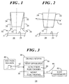
- FIG. 1 shows a cross-sectional view of a beam element 20 having asymmetrically tilted sidewalls 22, 24 and FIG. 2 shows a cross-sectional view of beam element 20 exemplifying its movement in response to the asymmetrically tilted sidewalls 22, 24.
- Sidewalls 22, 24 are tilted away from a design orientation, represented by a dashed line 26.
- the degree of tilt is referred to as a skew angle, ⁇ .
- sidewall 22 tilts inwardly at a skew angle 28, ⁇ R
- sidewall 24 tilts inwardly at a skew angle 30, ⁇ L .
- skew angle 28 defines a degree to which sidewall 22 is nonparallel relative to an axis, i.e. dashed line 26, perpendicular to a planar surface 29 of an underlying substrate 31.
- skew angle 30 defines a degree to which sidewall 24 is nonparallel relative to an axis, i.e. dashed line 26, perpendicular to planar surface 29 of the underlying substrate 31.
- Skew angle 28 may not be equivalent to skew angle 30.
- skew angle 28 is greater than skew angle 30.
- the asymmetrically tilted etch profile of beam element 20 can lead to a shift of the principle axis 32.
- This shift in the principle axis 32 can cause the in-plane motion of beam element 20 to couple to out-of-plane motion which contributes to quadrature error.
- the out-of-plane motion is represented by a tilted bi-directional arrow 33 in FIG. 2 .
- skew angles 28 and 30 in the sidewalls of some MEMS devices, e.g., angular rate sensors, resulting from inadequate dimensional precision during manufacturing can be crucial for understanding the impact of quadrature error in the MEMS devices.
- skew angles 28 and 30 can be added to the geometry of the angular rate sensor model. Numerical simulations can be run on the angular rate sensor model to predict how much quadrature error the angular rate sensor design produces with the given skew angles 28 and 30.
- skew angles 28 and 30 are not readily measured directly through cross sectioning since they can be very small. For example, skew angles 28 and 30 can be on the order of 0.2 degrees.
- Other methodologies entail probing the MEMS device, such as a MEMS angular rate sensor, to determine the severity of quadrature error.
- these methodologies call for vacuum seal of the MEMS device or a specialized probe chamber, and sophisticated measurement capabilities.
- Embodiments entail a test apparatus, a test system, and methodology for estimating skew angles in a sidewall of a MEMS device that result from a particular etch process that may be used to fabricate the MEMS device, and fabricating MEMS devices based on the results of the methodology.
- the test apparatus, test system, and methodology are implemented to estimate sidewall skew angles from a static probe measurement in ambient conditions.
- the test apparatus design can enable estimation of the sidewall skew angle to within approximately ten percent in any location on a device wafer that the test apparatus is fabricated. Accordingly, results of the test methodology can be evaluated to ascertain the efficacy of a particular etch process and/or to test improvements to an etch process in order to reduce the skew angles to an acceptable range.
- test apparatus test system, and methodology for estimating the sidewall skew angle may be implemented with a variety of MEMS devices, e.g., angular rate sensors, optical devices, and so forth, where in-plane to out-of-plane coupling (resulting from manufacturing imperfections that permit the suspended mass to move out-of-plane of its intended drive motion) can adversely affect the output and/or operation of the MEMS device.
- MEMS devices e.g., angular rate sensors, optical devices, and so forth, where in-plane to out-of-plane coupling (resulting from manufacturing imperfections that permit the suspended mass to move out-of-plane of its intended drive motion) can adversely affect the output and/or operation of the MEMS device.
- FIG. 3 shows a block diagram of a test system 34 for estimating a skew angle in a sidewall of a beam formed using an etch process in accordance with an embodiment.
- test system 34 includes a test apparatus 36 contained on a device wafer 38. Test apparatus 36 may be formed using a particular etch process under evaluation. Test system 34 further includes a voltage source 40 for providing an actuation signal 42, for example, a direct current (DC) voltage signal 42, to actuation electrodes 44 of test apparatus 36. Additionally, test system 34 includes test equipment 46 for receiving signals, for example, a capacitance signal 48 (represented by "C") from sense electrodes 50 of test apparatus 36. For purposes of illustration, capacitance signal 48 is referred to herein as a baseline capacitance signal 48. In accordance with a skew angle evaluation process, a change in capacitance from baseline capacitance signal 48 may be measured, as discussed in greater detail below.
- test apparatus 36 includes a mechanical amplification structure (discussed below) that is actuated via voltage source 40.
- the mechanical amplification structure applies a relatively large amount of in-plane bending to one or more beams. This large static in-plane bending produces out-of-plane motion if the beam has a sidewall skew angle, or more particularly, when asymmetrically tilted etch patterns (shown in FIGs. 1 and 2 ), are formed in the sidewalls of the beam.
- the degree of out-of-plane motion is related to the skew angle.
- Test equipment 46 may be used to measure the vertical motion of the tip of the beam to infer the skew angle.
- sense electrodes 50 are capacitive sensors that are formed at some advantageous position proximate the mechanical amplification structure to sense the vertical (i.e., out-of-plane) motion and communicate capacitance signal 48 to test apparatus 36.
- Test apparatus 36 includes one or more structures formed on a substrate of device wafer 38 using a particular etch process under evaluation. These one or more structures can be formed at suitable locations on the substrate in order to estimate skew angles resulting from the etch process over a wide surface area of the substrate. Test apparatus 36 is independent from the MEMS devices to be fabricated using the etch process under evaluation. Hence, in some embodiments, device wafer 38 may be a device wafer upon which only test apparatuses 36 are formed. In other embodiments, device wafer 38 may be a device wafer upon which MEMS devices (e.g., angular rate sensors), generally represented by a reference numeral 51, are co-located with one or more test apparatuses 36. However, test apparatuses 36 are located in different physical positions on the substrate from MEMS devices (51).
- MEMS devices e.g., angular rate sensors
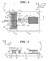
- FIG. 4 shows a top view of one of test apparatuses 36 for estimating a skew angle in accordance with an embodiment
- FIG. 5 shows a side view of test apparatus 36 along section lines 5-5 of FIG. 4
- Test apparatus 36 generally includes a motion amplification structure 52 suspended above a substrate 53, an actuator 54, and at least one sense electrode 50 formed on a planar surface 56 of substrate 53.
- device wafer 38 may contain only test apparatuses 36.
- device wafer 38 may contain one or more test apparatuses 36 co-located with, but independent from, MEMS devices 51 ( FIG. 3 ) also formed on substrate 53. As such, only a portion of device wafer 38 including one of test apparatuses 36 is shown for simplicity of illustration.
- Motion amplification structure 52 includes a first beam 58, a second beam 60, and a paddle element 62.
- First beam 58 has a first movable end 64, a middle region 66 configured to flex, and a second end 68.
- Second beam 60 has a third end 70 fixed to substrate 53 via an anchor 72 and a fourth end 74. Second end 68 of first beam 58 and fourth end 74 of second beam 60 are connected to paddle element 62.
- first and second beams 58 and 60 are adjacent to one another such that second end 68 of first beam 58 and fourth end 74 of second beam 60 are coupled to a common edge 76 (i.e., the same edge) of paddle element 62.
- first and second beams 58 and 60 may not be adjacent to one another.
- Sense electrode 50 is positioned on surface 56 of substrate 53 underlying the suspended paddle element 62.
- test apparatus 36 Various components of test apparatus 36 are illustrated with different shading and/or hatching to distinguish the different elements produced within the structural layers of test apparatus 36 from one another. These different elements within the structural layers may be produced utilizing the surface micromachining techniques of depositing, patterning, etching, and so forth. Accordingly, although different shading and/or hatching is utilized in the illustrations, the different elements within the structural layers are typically formed out of the same material, such as polysilicon, single crystal silicon, and the like.
- test apparatus 36 may be described variously as being “attached to,” “attached with,” “coupled to,” “connected to,” or “interconnected with,” other elements of test apparatus 36. However, it should be understood that the terms refer to the direct or indirect physical connections of particular elements of test apparatus 36 that occur during their formation through the deposition, patterning, and etching processes of MEMS fabrication.
- Actuator 54 includes a movable element 80 suspended above substrate 53 and coupled to first end 64 of first beam 58.
- Actuator 54 further includes one or more anchor elements 82 fixed to substrate 53 and compliant members 84 interconnected between movable element 80 and anchor elements 82.
- Actuator 54 additionally includes one or more actuation electrodes 44 positioned proximate movable element 80.
- movable element 80 is a frame structure having multiple openings 86, with one of actuation electrodes 44 positioned within each of openings 86.
- movable element 80 and actuation electrodes 44 can vary greatly in other embodiments.
- each of openings 86 may include two adjacent actuation electrodes 44 suitably arranged to enable bidirectional actuation.
- Conductive traces, pads, interconnects, test points, and so forth may be formed on, in, or proximate to substrate 53 in a known manner for use in forming an electrically conductive pathway between voltage source 40 ( FIG. 3 ) and actuation electrodes 44.
- test apparatus 36 The cross-sectional side view of test apparatus 36 shown in FIG. 5 reveals the fixed connection of sense electrode 50, anchor 72 (coupled to third end 70 of second beam 60), and actuation electrodes 44 to surface 56 of substrate 53. Additionally, the side view of test apparatus 36 reveals the suspended configuration of paddle element 62, movable element 80, and compliant members 84 above surface 56 of substrate 53. Although not visible in the side view, first and second beams 58 and 60 are suspended above surface 56 of substrate 53 in a similar manner. Test apparatus 36 can be formed using conventional surface micromachining techniques involving sacrificial material deposition, patterning, and etching to achieve the released and suspended structures of beams 58, 60, paddle element 62, movable element 80, and compliant members 84.
- actuation signal 42 ( FIG. 3 ) is applied to actuation electrodes 44.
- Actuation signal 42 enables motion of movable element 80 relative to fixed anchor elements 82 by electrostatic force. That is, compliant members 84 flex to enable planar motion of movable element 80 toward first beam 58. Since movable element 80 is coupled to first end 64 of first beam 58, the motion of movable element 80 induces an axial force, represented by an arrow 88 in FIG. 1 , upon first end 64 of first beam 58.
- a three-dimensional coordinate system is provided showing an X-axis 90, a Y-axis 92, and a Z-axis 94, where Z-axis 94 is perpendicular to surface 56 of substrate 53.
- Test apparatus 36 is thus illustrated as having a generally planar structure within an X-Y plane 96, where X-axis 90 and Y-axis 92 are substantially parallel to surface 56 of substrate 53 and Z-axis 94 extends perpendicular to X-Y plane 96.
- axial force 88 is oriented approximately parallel to X-axis 90, and is thus parallel to planar surface 56.
- a height of compliant members 84 in a direction parallel to Z-axis 94 is significantly greater than their width in a direction parallel to X-axis 90.
- a length of compliant members 84 in a direction parallel to Y-axis 92 is significantly greater than both the height and width of compliant members 84. Accordingly, compliant members 84 are flexible to allow motion of movable element 80 toward first end 64 of first beam in order to induce axial force 88.
- compliant elements 84 are relatively stiff in a direction perpendicular to surface 56 (i.e., in a direction parallel to Z-axis 94) to prevent or limit electrostatic levitation of movable element 80.
- compliant elements 84 can be configured in a great variety of shapes and orientations, and to have any suitable stiffness that enables motion of movable element 80.
- first beam 58 When axial force 88 is a compressive axial force which exceeds a critical value, first beam 58 is compressed axially along its length, L 1 , and the movable first end 64 displaces axially (i.e., in a direction parallel to X-axis 90). Similarly, when axial force 88 is a tensile axial force with exceeds the critical value, first beam 58 is pulled axially (i.e., in a direction parallel to X-axis 90) and again, the movable first end 64 displaces axially. Second end 68 is effectively fixed due to its interconnection with paddle element 62, second beam 60, and anchor 72.
- the axial displacement of the movable first end 64 of first beam 58 in response to either a compressive or a tensile axial force 88) can cause middle region 66 of first beam 58, as well as second beam 60, to buckle or flex transversely within X-Y plane 96.
- This flexion is referred to herein as in-plane motion, where the in-plane motion is approximately parallel to planar surface 56.
- any combination of skew angles in sidewalls 98 (best represented in FIG. 7 ) of first and/or second beams 58 and 60 resulting from the particular etch process used to form test apparatus 36 can produce displacement of the tip of motion amplification structure 52, namely paddle element 62.
- the displacement of paddle element 62 is a vertical displacement generally parallel to Z-axis 94.
- the displacement of paddle element 62 is referred to herein as out-of-plane motion, where the out-of-plane motion is approximately perpendicular to planar surface 96.
- the displacement of paddle element 62 is sensed at sense electrode 50 as a capacitance change signal.
- the magnitude of displacement i.e., a change in capacitance from baseline capacitance signal 48, corresponds to the degree of the skew angle formed in either or both of sidewalls 98 of first and second beams 58 and 60.
- the dual beams 58, 60 and paddle element 62 of motion amplification structure 52 enables a relatively large amount of in-plane motion to one or both beams 58 and 60.
- This relatively large in-plane motion produces out-of-plane motion of paddle element 62 if beams 58, 60 have a sidewall skew angle resulting from the etch process.
- the degree of out-of-plane motion is related to the size of the skew angle, and therefore measurement of the vertical motion of paddle element 62 can be used to estimate the skew angle.
- test apparatus 36 may be utilized within test system 34 to estimate skew angles resulting from an etch process in order to determine whether the etch process is suitable or the etch process needs improvement.
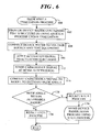
- FIG. 6 shows a flowchart of a skew angle evaluation process 100 utilizing test apparatus 36 ( FIG. 4 ) in accordance with an embodiment.
- Skew angle evaluation process 100 may be performed utilizing test system 34 ( FIG. 3 ) containing test apparatus 36 ( FIG. 4 ) to estimate a skew angle produced by a particular etch process.
- the results of the test methodology can evaluated to ascertain the efficacy of a particular etch process and/or to test improvements to an etch process in order to reduce the skew angles to an acceptable range.
- MEMS devices 51 FIG. 3
- Skew angle evaluation process 100 begins with a task 102.
- a device wafer e.g., device wafer 38 ( FIG. 3 ), containing at least one of test structures 36 ( FIG. 4 ) is provided.
- Device wafer 38 is formed using a particular etch process under evaluation.
- the etch process may be, for example, a deep reactive ion etch (DRIE) process, or any other process implemented to form the suspended structures of MEMS devices 51.
- the facility executing skew angle evaluation process 100 may also be the facility that formed device wafer 38.
- device wafer 38 containing at least one of test structures 36 may be provided by another fabrication facility for evaluation.
- Process 100 continues with a task 104.
- device wafer 38 is suitably connected to voltage source 40 ( FIG. 3 ) and test equipment 46 ( FIG. 3 ) within test system 34 ( FIG. 3 ).
- Task 104 may be performed in a conventional test environment without the need for test apparatus(es) 36 contained on device wafer 38 to be in a vacuum sealed environment or in a specialized probe chamber.
- a task 106 is performed.
- actuation signal 42 ( FIG. 3 ), e.g., a DC bias voltage, is applied to actuation electrodes 44 ( FIG. 4 ).
- FIG. 7 shows a perspective view of motion amplification structure 52 implemented within test apparatus 36 ( FIG. 4 ) and FIG. 8 shows a side view of a portion of motion amplification structure 52 along section lines 8-8 of FIG. 7 .
- Application of actuation signal 42 ( FIG. 3 ) induces axial force 88 upon first end 64 of first beam 58 to cause flexion, i.e., in-plane motion 108, of middle region 66 of first beam 58 and potentially second beam 60.
- axial force 88 is a tensile axial force.
- actuation electrodes 44 FIG.
- in-plane motion 108 produces displacement, i.e., out-of-plane motion 110 ( FIG. 8 ) of paddle element 62.
- a task 112 is performed in connection with task 106.
- the displacement, i.e., out-of-plane motion 110, of paddle element 62 is sensed at sense electrodes 50 as a capacitance change signal 114, dC, between paddle element 62 and the underlying sense electrode 50 relative to baseline capacitance value 48 ( FIG. 3 ).
- Capacitance change signal 114 at sense electrode 50 may be measured using a conventional test probe of test equipment 46 ( FIG. 3 ).
- skew angle evaluation process 100 continues with a task 116.
- capacitance change signal 114 is compared to a model of capacitance changes versus skew angles for test apparatus 36 ( FIG. 4 ) to estimate a skew angle for first beam 58.
- FIG. 9 shows a plot 118 of simulation results that may be utilized to estimate a skew angle.
- plot 118 includes a horizontal axis of skew angles 120, ⁇ , versus a vertical axis of capacitance change values 122, dC.
- Skew angles 120 are centered at ninety degrees, where ninety degrees corresponds to the axis perpendicular to planar surface 56 ( FIG. 4 ), i.e., Z-axis 94.
- skew angle 120 at ninety degrees corresponds to no skew angle, i.e., a skew angle equal to zero.
- the capacitance when the skew angle is zero can be any baseline capacitance value 48 ( FIG. 3 ) specific to test apparatus 36.
- the vertical axis of plot 118 represents a change (i.e., a difference value) between baseline capacitance value 48 and a change in capacitance in response to the displacement, i.e., out-of-plane motion 110, of paddle element 62 ( FIG. 4 ).
- finite element analysis may be utilized to determine a correlation between capacitance change for a particular test apparatus 36 and the skew angle.
- the skew angle measurement structure i.e., test structure 36
- the skew angle measurement structure may be modeled to include one of skew angles 120 and then simulated for in-plane deformations, i.e., in-plane motion 108 ( FIG. 7 ) that correspond to the limits of travel set by the design of test structure 36.
- Plot 118 indicates the simulation results that form a transfer function 124 between capacitance change 122 and skew angle 120.
- the correlation between the capacitance measurements from test structure 36, i.e., capacitance change signal 114 ( FIG. 8 ) and the skew angle on test structure 36, can be determined using plot 118. That is, once capacitance change signal 114 ( FIG. 8 ) is measured at task 112, the measured capacitance change signal 114 can be correlated with skew angles 120 in plot 118 in order to estimate a skew angle of first beam 58 ( FIG. 4 ).
- transfer function 124 reveals an estimated skew angle 126 of approximately 0.1 degrees.
- skew angle evaluation process 100 continues with a query task 128.
- estimated skew angle 126 is evaluated to determine whether it is within an allowable skew angle range. In this example, a determination is made as to whether estimated skew angle 126 is within an allowable range of skew angles. As shown in plot 118, an allowable range 130 of skew angles 120 may be ⁇ 0.2 degrees.
- process 100 continues with a task 132.
- the etch process used to form test apparatus 36 ( FIG. 4 ) maybe accepted for use in producing MEMS devices 51 ( FIG. 3 ).
- a block 136 of process 100 indicates that a MEMS device fabrication process using the accepted etch process is performed to produce the MEMS devices 51.
- MEMS device fabrication process 136 are not provided in detail herein for brevity. However, it should be understood the same fabrication processes used to fabricate test apparatus 36 may be implemented to fabricate MEMS devices 51. In particular, the same etch process that was evaluated in connection with skew angle evaluation process 100 can be implemented to fabricate MEMS devices 51.
- process 100 continues with a task 134 when estimated skew angle 126 falls outside of allowable range 130 as determined at query task 128.
- the etch process used to form test apparatus 36 may be rejected for use in producing MEMS devices 51. That is, the etch process may need improvement in order to get an acceptably reduced skew angle.
- skew angle evaluation process 100 ends.
- estimated skew angle 126 may additionally be added to the geometry of the MEMS device, e.g., angular rate sensor, model. Numerical simulations may then be run to predict how much quadrature error the design produces with estimated skew angle 126.
- skew angle evaluation process 100 can be executed to characterize the sidewall skew angle resulting from a particular etch process. If the etch process cannot be improved to reduce the sidewall skew angle, the quadrature error may be too great.
- FIG. 10 shows a top view of a test apparatus 140 in accordance with another embodiment.
- Test apparatus 140 includes multiple motion amplification structures 52 suspended above surface 56 of substrate 53, where each of the multiple motion amplification structures 52 includes first beam 58, second beam 60, and paddle element 62.
- test apparatus 140 further includes a plurality of sense electrodes 50, one each of sense electrodes 50 being in proximity to one each of paddle elements 62.
- sense electrodes are formed on surface 56 of substrate 53 underlying paddle elements 62.
- Test apparatus 140 employs four motion amplification structures 52 and the corresponding sense electrodes 50 so that test apparatus 140 can evaluate skew angles relative to two axes, i.e., X-axis 90 and Y-axis 92, and so that test apparatus 140 is approximately twice as sensitive to skew angles in each of the two axes.
- test apparatus 140 includes a motion amplification structure 52, referred to herein as a first motion amplification structure 52A, and another motion amplification structure 52, referred to herein as a second motion amplification structure 52B, aligned with first motion amplification structure 52A.
- Test apparatus 140 further includes a motion amplification structure 52, referred to herein as a third motion amplification structure 52C, and another motion amplification structure 52, referred to herein as a fourth motion amplification structure 52D, aligned with third motion amplification structure 52C.
- Motion amplification structures 52A, 52B, 52C, and 52D are arranged such that first beams 58 of structures 52A, 52B, 52C, and 52D are connected at a central location 142 of test apparatus 140.
- each of motion amplification structures 52A, 52B, 52C, and 52D has a longitudinal axis 144 aligned with each respective first beam 58.
- Longitudinal axis 144 of first and second motion amplification structures 52A and 52B is aligned with an axis that is parallel to planar surface 56 of substrate 53.
- longitudinal axis 144 of first and second motion amplification structures 52A and 52B is aligned with, i.e., parallel to, X-axis 90.
- longitudinal axis 144 of third and fourth motion amplification structures 52C and 52D is aligned with an axis that is parallel to planar surface 56 of substrate 53.
- third and fourth motion amplification structures 52C and 52D are aligned with, i.e., parallel to, Y-axis 92.
- third and fourth motion amplification structures 52C and 52D are oriented generally perpendicular to first and second motion amplification structures 52A and 52B.
- Test apparatus 140 further includes actuator 54, in the form of four electrode banks 146 that are interconnected by a rigid frame 148.
- Each of electrode banks 146 includes a movable element 150 and actuation electrodes 44 in proximity to movable element 150, as discussed above in connection with FIG. 4 .
- Compliant members 152 are interconnected between movable element 150 and anchor elements 154 fixed to substrate 53. Additional compliant members 156 may also be furnished to support some of electrode banks 146 of actuator 54.
- Movable element 150 of each electrode bank 146 is coupled to first beam 58 of each of motion amplification structures 52A, 52B, 52C, and 52D at central location 142.
- Actuator 54, containing multiple electrode banks 146 may be activated by the application of actuation signal 42 ( FIG. 3 ) on actuation electrodes 44.
- electrode banks 146 may be oriented diagonal to corresponding pairs of motion amplification structures 52A, 52B, 52C, and 52D.
- actuation signal 42 enables motion of movable elements 150 of the four electrode banks 146 in a direction 158 that is approximately parallel to X-Y plane 96 and that is approximately diagonal to each of X- and Y-axes 90, 92.
- actuator 54 is operative on each of first beams 58 of motion amplification structures 52A, 52B, 52C, and 52D such that activation of actuator 54 induces at least a portion of axial force 88 upon first ends 64 of first beams 58 to cause in-plane motion 108 of middle regions 66 of first beams 58. That is, the diagonal direction 158 of motion of movable elements 150 imparts a vector portion of axial force 88 upon first ends 64 of first beams 58.
- first beams 58 of motion amplification structures 52A, 52B, 52C, and 52D has one or more sidewalls 98 that exhibits a skew angle
- flexion of first beam 58 produces displacement of the its corresponding paddle element 62.
- the displacement of corresponding paddle element 62 is subsequently sensed as capacitance change 114 ( FIG. 8 ) at the corresponding sense electrode 50.
- FIG. 11 shows a plot 160 of simulation results that may be utilized to estimate a skew angle in one direction
- FIG. 12 shows a plot 162 of simulation results that may be utilized to estimate a skew angle in another direction.
- Plots 160 and 162 may be utilized in connection with skew angle evaluation process 100 ( FIG. 6 ) when evaluating skew angles using the dual axis configuration of test apparatus 140 ( FIG. 10 ).
- Each of plots, 160 and 162 includes a horizontal axis of skew angles 120, ⁇ , versus a vertical axis of capacitance change values 122, dC.
- skew angles 120 are centered at ninety degrees, where ninety degrees corresponds to the axis perpendicular to planar surface 56 ( FIG. 4 ), i.e., Z-axis 94.
- the vertical axis in each of plots 160 and 162 represents the change (i.e., a difference value) between baseline capacitance value 48 and a change in capacitance in response to the displacement.
- Plot 160 indicates the simulation results that form a transfer function 164 between capacitance change 122 and skew angle 120 for third and fourth motion amplification structures 52C and 52D ( FIG. 10 ) in the Y-direction.
- Plot 160 further indicates that first and second motion amplification structures 52A and 52B longitudinally aligned with X-axis 90 ( FIG. 10 ) are largely insensitive to sidewall skew angles in the Y direction.
- plot 162 indicates the simulation results that form another transfer function 166 between capacitance change 122 and skew angle 120 for first and second motion amplification structures 52A and 52B ( FIG. 10 ) in the X-direction.
- Plot 162 further indicates that third and fourth motion amplification structures 52C and 52D longitudinally aligned with Y-axis 92 ( FIG. 10 ) are largely insensitive to sidewall skew angles in the X direction.
- An embodiment of a test apparatus comprises a motion amplification structure suspended above a substrate.
- the motion amplification structure includes a first beam, a second beam, and a paddle element.
- the first beam has a movable first end, a middle region configured to flex, and a second end.
- the second beam has a third end fixed to the substrate and a fourth end, wherein the second end of the first beam and the fourth end of the second beam are connected to the paddle element.
- the test apparatus further comprises an actuator operative upon the first beam such that activation of the actuator induces an axial force upon the first end of the first beam to cause flexion of the middle region, and a sense electrode in proximity to the paddle element, wherein when a sidewall of the first beam exhibits a skew angle relative to an axis perpendicular to a planar surface of the substrate, the flexion of the first beam produces displacement of the paddle element, the displacement of the paddle element being sensed at the sense electrode.
- An embodiment of test system for estimating a skew angle in a sidewall of a beam formed using an etch process comprises a test apparatus formed on a substrate using the etch process.
- the test apparatus includes a motion amplification structure suspended above the substrate, the motion amplification structure including a first beam, a second beam, and a paddle element.
- the first beam has a movable first end, a middle region configured to flex, and a second end.
- the second beam has a third end fixed to the substrate and a fourth end, wherein the second end of the first beam and the fourth end of the second beam are connected to the paddle element.
- the test apparatus further includes an actuator operative upon the first beam such that activation of the actuator induces axial force upon the first end of the first beam to cause flexion of the middle region, and a sense electrode in proximity to the paddle element, wherein when the first beam exhibits the skew angle, the flexion of the first beam produces displacement of the paddle element, the displacement of the paddle element being sensed at the sense electrode.
- the test system further includes test equipment in communication with the sense electrode for receiving a signal indicative of the displacement of the paddle element, wherein the skew angle defines a degree to which the sidewall of the first beam is offset from an axis perpendicular to a planar surface of the substrate, and the displacement corresponds to the degree of the sidewall skew angle.
- An embodiment of a method comprises providing device wafer containing a test apparatus, the test apparatus including a motion amplification structure suspended above a substrate of the device wafer, the motion amplification structure including a first beam, a second beam, and a paddle element, the first beam having a movable first end, a middle region configured to flex, and a second end, the second beam having a third end fixed to the substrate and a fourth end, wherein the second end of the first beam and the fourth end of the second beam are connected to the paddle element.
- the method further comprises inducing an axial force upon the first end of the first beam via an actuator to cause flexion of the middle region and determining a displacement of the paddle element in response to the axial force.
- Another embodiment of a method comprises providing a device wafer containing a test apparatus, the test apparatus including a motion amplification structure suspended above a substrate of the device wafer, the motion amplification structure including a first beam, a second beam, and a paddle element, wherein an etch process is used to produce the motion amplification structure, the first beam having a movable first end, a middle region configured to flex, and a second end, the second beam having a third end fixed to the substrate and a fourth end, the second end of the first beam and the fourth end of the second beam being connected to the paddle element.
- the method further comprises inducing an axial force upon the first end of the first beam to cause flexion of the middle region, determining a displacement of the paddle element in response to the axial force, and estimating a skew angle of a sidewall of the first beam in response to the displacement, the skew angle resulting from the etch process, and the skew angle defining a degree to which the sidewall of the first beam is nonparallel to an axis perpendicular to a planar surface of the substrate.
- the etch process is rejected for use in fabricating the MEMS device.
- the estimated skew angle is accepted for use in fabricating the MEMS device and the MEMS device is fabricated using the etch process.
- test apparatus test system, and methodology are implemented to estimate sidewall skew angles from a static probe measurement in ambient conditions.
- the test apparatus design can enable estimation of the sidewall skew angle to within approximately ten percent in any location on a device wafer that the test apparatus is fabricated. Accordingly, results of the test methodology can be evaluated to ascertain the efficacy of a particular etch process and/or to test improvements to an etch process in order to reduce the skew angles to an acceptable range.
Landscapes
- Engineering & Computer Science (AREA)
- Physics & Mathematics (AREA)
- General Physics & Mathematics (AREA)
- Radar, Positioning & Navigation (AREA)
- Remote Sensing (AREA)
- Manufacturing & Machinery (AREA)
- Microelectronics & Electronic Packaging (AREA)
- Pressure Sensors (AREA)
- Gyroscopes (AREA)
- Measurement Of Length, Angles, Or The Like Using Electric Or Magnetic Means (AREA)
- Length Measuring Devices With Unspecified Measuring Means (AREA)
Abstract
Description
- The present invention relates generally to microelectromechanical systems (MEMS) devices. More specifically, the present invention relates to the fabrication of MEMS devices that are less susceptible to quadrature error.
- Microelectromechanical systems (MEMS) technology has achieved wide popularity in recent years, as it provides a way to make very small mechanical structures and integrate these structures with electrical devices on a single substrate using conventional batch semiconductor processing techniques. One common application of MEMS is the design and manufacture of sensor devices. MEMS sensor devices are widely used in applications such as automotive, inertial guidance systems, household appliances, game devices, protection systems for a variety of devices, and many other industrial, scientific, and engineering systems. One example of a MEMS sensor is a MEMS angular rate sensor. An angular rate sensor senses angular speed or velocity around one or more axes. Other MEMS devices may be utilized as actuators, switches, pumps, and so forth.
- A more complete understanding of the present invention may be derived by referring to the detailed description and claims when considered in connection with the Figures, wherein like reference numbers refer to similar items throughout the Figures, the Figures are not necessarily drawn to scale, and:
-
FIG. 1 shows a cross-sectional view of a beam element of a microelectromechanical systems (MEMS) device having asymmetrically tilted sidewalls; -
FIG. 2 shows a cross-sectional view of the beam element ofFIG. 1 exemplifying its movement in response to the asymmetrically tilted sidewalls; -
FIG. 3 shows a block diagram of a test system for estimating a skew angle in a sidewall of a beam in accordance with an embodiment; -
FIG. 4 shows a top view of a test apparatus for estimating a skew angle in accordance with an embodiment; -
FIG. 5 shows a side view of the test apparatus ofFIG. 4 ; -
FIG. 6 shows a flowchart of a skew angle evaluation process in accordance with an embodiment; -
FIG. 7 shows a perspective view of a motion amplification structure implemented within the testiapparatus ofFIG. 4 ; -
FIG. 8 shows a side view of a portion of the motion amplification structure along section lines 8-8 ofFIG. 7 ; -
FIG. 9 shows a plot of simulation results that may be utilized to estimate a skew angle; -
FIG. 10 shows a top view of a test apparatus in accordance with another embodiment; -
FIG. 11 shows a plot of simulation results that may be utilized to estimate a skew angle in one direction; and -
FIG. 12 shows a plot of simulation results that may be utilized to estimate a skew angle in another direction. - In vibratory microelectromechanical systems (MEMS) angular rate sensors, an inherent problem is the existence of undesirable interference signals, referred to as a quadrature component or quadrature error. Quadrature error can occur in vibrating angular rate sensors due to manufacturing imperfections that permit the suspended mass to oscillate out-of-plane of its intended drive motion. This out-of-plane motion can create an oscillation about the sense axis that can be confused with Coriolis acceleration and subsequently, the rotation rate. Unfortunately, quadrature error can result in offset error, reduced dynamic range, and increased noise for the device. A large quadrature error may even cause a device to rail the electronic circuit due to significant vertical motion, so that in the worst case, the sense mass may come into contact with conductive electrodes potentially resulting in collision-related damage, such as a short.
- A major source for quadrature error is from inadequate dimensional precision during manufacturing. For example, off-vertical ion impact from deep reactive ion etch (DRIE) plasma during etching of the MEMS structural layer can produce asymmetrically tilted etch patterns in the sidewalls of the elements formed in the MEMS structural layer. The asymmetrical etch profile can lead to a shift of the principle axis. As such, in-plane motion couples to out-of-plane motion. The out-of-plane motion can be a major contributor to quadrature error in X- and Y-axis angular rate sensors with an out-of-plane sense mode.
- Referring to
FIGs. 1-2, FIG. 1 shows a cross-sectional view of abeam element 20 having asymmetrically tiltedsidewalls FIG. 2 shows a cross-sectional view ofbeam element 20 exemplifying its movement in response to the asymmetricallytilted sidewalls Sidewalls dashed line 26. The degree of tilt is referred to as a skew angle, α. In the illustration shown inFIG. 1 ,sidewall 22 tilts inwardly at askew angle 28, αR, andsidewall 24 tilts inwardly at askew angle 30, αL. Accordingly,skew angle 28 defines a degree to whichsidewall 22 is nonparallel relative to an axis, i.e. dashedline 26, perpendicular to aplanar surface 29 of anunderlying substrate 31. Likewise,skew angle 30 defines a degree to whichsidewall 24 is nonparallel relative to an axis, i.e. dashedline 26, perpendicular toplanar surface 29 of theunderlying substrate 31. -
Skew angle 28 may not be equivalent toskew angle 30. For example, as shown,skew angle 28 is greater thanskew angle 30. This results in an uneven, i.e., an asymmetrically tilted, etch pattern inbeam element 20. As shown inFIG. 2 , the asymmetrically tilted etch profile ofbeam element 20 can lead to a shift of theprinciple axis 32. This shift in theprinciple axis 32 can cause the in-plane motion ofbeam element 20 to couple to out-of-plane motion which contributes to quadrature error. The out-of-plane motion is represented by a tiltedbi-directional arrow 33 inFIG. 2 . - Knowledge of
skew angles skew angles skew angles - Attempts have been made to directly measure the skew angles of a structure, such as
beam element 20 in order to characterize the potential for quadrature error. However,skew angles skew angles - Embodiments entail a test apparatus, a test system, and methodology for estimating skew angles in a sidewall of a MEMS device that result from a particular etch process that may be used to fabricate the MEMS device, and fabricating MEMS devices based on the results of the methodology. The test apparatus, test system, and methodology are implemented to estimate sidewall skew angles from a static probe measurement in ambient conditions. The test apparatus design can enable estimation of the sidewall skew angle to within approximately ten percent in any location on a device wafer that the test apparatus is fabricated. Accordingly, results of the test methodology can be evaluated to ascertain the efficacy of a particular etch process and/or to test improvements to an etch process in order to reduce the skew angles to an acceptable range.
- The test apparatus, test system, and methodology for estimating the sidewall skew angle may be implemented with a variety of MEMS devices, e.g., angular rate sensors, optical devices, and so forth, where in-plane to out-of-plane coupling (resulting from manufacturing imperfections that permit the suspended mass to move out-of-plane of its intended drive motion) can adversely affect the output and/or operation of the MEMS device.
-
FIG. 3 shows a block diagram of atest system 34 for estimating a skew angle in a sidewall of a beam formed using an etch process in accordance with an embodiment. In general,test system 34 includes atest apparatus 36 contained on adevice wafer 38.Test apparatus 36 may be formed using a particular etch process under evaluation.Test system 34 further includes avoltage source 40 for providing anactuation signal 42, for example, a direct current (DC)voltage signal 42, toactuation electrodes 44 oftest apparatus 36. Additionally,test system 34 includestest equipment 46 for receiving signals, for example, a capacitance signal 48 (represented by "C") fromsense electrodes 50 oftest apparatus 36. For purposes of illustration,capacitance signal 48 is referred to herein as abaseline capacitance signal 48. In accordance with a skew angle evaluation process, a change in capacitance frombaseline capacitance signal 48 may be measured, as discussed in greater detail below. - In general,
test apparatus 36 includes a mechanical amplification structure (discussed below) that is actuated viavoltage source 40. The mechanical amplification structure applies a relatively large amount of in-plane bending to one or more beams. This large static in-plane bending produces out-of-plane motion if the beam has a sidewall skew angle, or more particularly, when asymmetrically tilted etch patterns (shown inFIGs. 1 and 2 ), are formed in the sidewalls of the beam. The degree of out-of-plane motion is related to the skew angle.Test equipment 46 may be used to measure the vertical motion of the tip of the beam to infer the skew angle. In some embodiments,sense electrodes 50 are capacitive sensors that are formed at some advantageous position proximate the mechanical amplification structure to sense the vertical (i.e., out-of-plane) motion and communicatecapacitance signal 48 to testapparatus 36. -
Test apparatus 36 includes one or more structures formed on a substrate ofdevice wafer 38 using a particular etch process under evaluation. These one or more structures can be formed at suitable locations on the substrate in order to estimate skew angles resulting from the etch process over a wide surface area of the substrate.Test apparatus 36 is independent from the MEMS devices to be fabricated using the etch process under evaluation. Hence, in some embodiments,device wafer 38 may be a device wafer upon which only testapparatuses 36 are formed. In other embodiments,device wafer 38 may be a device wafer upon which MEMS devices (e.g., angular rate sensors), generally represented by a reference numeral 51, are co-located with one ormore test apparatuses 36. However,test apparatuses 36 are located in different physical positions on the substrate from MEMS devices (51). - Referring to
FIGs. 4 and 5, FIG. 4 shows a top view of one oftest apparatuses 36 for estimating a skew angle in accordance with an embodiment, andFIG. 5 shows a side view oftest apparatus 36 along section lines 5-5 ofFIG. 4 .Test apparatus 36 generally includes amotion amplification structure 52 suspended above asubstrate 53, anactuator 54, and at least onesense electrode 50 formed on aplanar surface 56 ofsubstrate 53. As mentioned previously,device wafer 38 may containonly test apparatuses 36. Alternatively,device wafer 38 may contain one ormore test apparatuses 36 co-located with, but independent from, MEMS devices 51 (FIG. 3 ) also formed onsubstrate 53. As such, only a portion ofdevice wafer 38 including one oftest apparatuses 36 is shown for simplicity of illustration. -
Motion amplification structure 52 includes afirst beam 58, asecond beam 60, and apaddle element 62.First beam 58 has a firstmovable end 64, a middle region 66 configured to flex, and asecond end 68.Second beam 60 has athird end 70 fixed tosubstrate 53 via ananchor 72 and afourth end 74.Second end 68 offirst beam 58 andfourth end 74 ofsecond beam 60 are connected to paddleelement 62. In an embodiment, first andsecond beams second end 68 offirst beam 58 andfourth end 74 ofsecond beam 60 are coupled to a common edge 76 (i.e., the same edge) ofpaddle element 62. However, in other embodiments, first andsecond beams Sense electrode 50 is positioned onsurface 56 ofsubstrate 53 underlying the suspendedpaddle element 62. - Various components of
test apparatus 36 are illustrated with different shading and/or hatching to distinguish the different elements produced within the structural layers oftest apparatus 36 from one another. These different elements within the structural layers may be produced utilizing the surface micromachining techniques of depositing, patterning, etching, and so forth. Accordingly, although different shading and/or hatching is utilized in the illustrations, the different elements within the structural layers are typically formed out of the same material, such as polysilicon, single crystal silicon, and the like. - In addition, the terms "first," "second," "third," "fourth," et cetera used herein do not refer to an ordering or prioritization of elements within a countable series of elements. Rather, the terms "first," "second," "third," and "fourth," are used to distinguish the particular elements for clarity of discussion. The elements of
test apparatus 36 may be described variously as being "attached to," "attached with," "coupled to," "connected to," or "interconnected with," other elements oftest apparatus 36. However, it should be understood that the terms refer to the direct or indirect physical connections of particular elements oftest apparatus 36 that occur during their formation through the deposition, patterning, and etching processes of MEMS fabrication. -
Actuator 54 includes amovable element 80 suspended abovesubstrate 53 and coupled tofirst end 64 offirst beam 58.Actuator 54 further includes one ormore anchor elements 82 fixed tosubstrate 53 andcompliant members 84 interconnected betweenmovable element 80 andanchor elements 82.Actuator 54 additionally includes one ormore actuation electrodes 44 positioned proximatemovable element 80. - In some embodiments,
movable element 80 is a frame structure havingmultiple openings 86, with one ofactuation electrodes 44 positioned within each ofopenings 86. However,movable element 80 andactuation electrodes 44 can vary greatly in other embodiments. For example, in some embodiments, each ofopenings 86 may include twoadjacent actuation electrodes 44 suitably arranged to enable bidirectional actuation. Conductive traces, pads, interconnects, test points, and so forth (not shown) may be formed on, in, or proximate tosubstrate 53 in a known manner for use in forming an electrically conductive pathway between voltage source 40 (FIG. 3 ) andactuation electrodes 44. - The cross-sectional side view of
test apparatus 36 shown inFIG. 5 reveals the fixed connection ofsense electrode 50, anchor 72 (coupled tothird end 70 of second beam 60), andactuation electrodes 44 to surface 56 ofsubstrate 53. Additionally, the side view oftest apparatus 36 reveals the suspended configuration ofpaddle element 62,movable element 80, andcompliant members 84 abovesurface 56 ofsubstrate 53. Although not visible in the side view, first andsecond beams surface 56 ofsubstrate 53 in a similar manner.Test apparatus 36 can be formed using conventional surface micromachining techniques involving sacrificial material deposition, patterning, and etching to achieve the released and suspended structures ofbeams paddle element 62,movable element 80, andcompliant members 84. - As will be discussed in greater detail below, actuation signal 42 (
FIG. 3 ) is applied toactuation electrodes 44.Actuation signal 42 enables motion ofmovable element 80 relative to fixedanchor elements 82 by electrostatic force. That is,compliant members 84 flex to enable planar motion ofmovable element 80 towardfirst beam 58. Sincemovable element 80 is coupled tofirst end 64 offirst beam 58, the motion ofmovable element 80 induces an axial force, represented by anarrow 88 inFIG. 1 , uponfirst end 64 offirst beam 58. - In the exemplary embodiment, a three-dimensional coordinate system is provided showing an X-axis 90, a Y-
axis 92, and a Z-axis 94, where Z-axis 94 is perpendicular to surface 56 ofsubstrate 53.Test apparatus 36 is thus illustrated as having a generally planar structure within anX-Y plane 96, whereX-axis 90 and Y-axis 92 are substantially parallel to surface 56 ofsubstrate 53 and Z-axis 94 extends perpendicular toX-Y plane 96. - In the exemplary embodiment,
axial force 88 is oriented approximately parallel toX-axis 90, and is thus parallel toplanar surface 56. A height ofcompliant members 84 in a direction parallel to Z-axis 94 is significantly greater than their width in a direction parallel toX-axis 90. Additionally, a length ofcompliant members 84 in a direction parallel to Y-axis 92 is significantly greater than both the height and width ofcompliant members 84. Accordingly,compliant members 84 are flexible to allow motion ofmovable element 80 towardfirst end 64 of first beam in order to induceaxial force 88. However,compliant elements 84 are relatively stiff in a direction perpendicular to surface 56 (i.e., in a direction parallel to Z-axis 94) to prevent or limit electrostatic levitation ofmovable element 80. Those skilled in the art will recognize thatcompliant elements 84 can be configured in a great variety of shapes and orientations, and to have any suitable stiffness that enables motion ofmovable element 80. - When
axial force 88 is a compressive axial force which exceeds a critical value,first beam 58 is compressed axially along its length, L1, and the movablefirst end 64 displaces axially (i.e., in a direction parallel to X-axis 90). Similarly, whenaxial force 88 is a tensile axial force with exceeds the critical value,first beam 58 is pulled axially (i.e., in a direction parallel to X-axis 90) and again, the movablefirst end 64 displaces axially.Second end 68 is effectively fixed due to its interconnection withpaddle element 62,second beam 60, andanchor 72. Accordingly, the axial displacement of the movablefirst end 64 of first beam 58 (in response to either a compressive or a tensile axial force 88) can cause middle region 66 offirst beam 58, as well assecond beam 60, to buckle or flex transversely withinX-Y plane 96. This flexion is referred to herein as in-plane motion, where the in-plane motion is approximately parallel toplanar surface 56. - Any combination of skew angles in sidewalls 98 (best represented in
FIG. 7 ) of first and/orsecond beams test apparatus 36 can produce displacement of the tip ofmotion amplification structure 52, namely paddleelement 62. The displacement ofpaddle element 62 is a vertical displacement generally parallel to Z-axis 94. Thus, the displacement ofpaddle element 62 is referred to herein as out-of-plane motion, where the out-of-plane motion is approximately perpendicular toplanar surface 96. The displacement ofpaddle element 62 is sensed atsense electrode 50 as a capacitance change signal. The magnitude of displacement, i.e., a change in capacitance frombaseline capacitance signal 48, corresponds to the degree of the skew angle formed in either or both ofsidewalls 98 of first andsecond beams - The
dual beams paddle element 62 ofmotion amplification structure 52 enables a relatively large amount of in-plane motion to one or bothbeams paddle element 62 ifbeams paddle element 62 can be used to estimate the skew angle. Accordingly,test apparatus 36 may be utilized withintest system 34 to estimate skew angles resulting from an etch process in order to determine whether the etch process is suitable or the etch process needs improvement. -
FIG. 6 shows a flowchart of a skewangle evaluation process 100 utilizing test apparatus 36 (FIG. 4 ) in accordance with an embodiment. Skewangle evaluation process 100 may be performed utilizing test system 34 (FIG. 3 ) containing test apparatus 36 (FIG. 4 ) to estimate a skew angle produced by a particular etch process. The results of the test methodology can evaluated to ascertain the efficacy of a particular etch process and/or to test improvements to an etch process in order to reduce the skew angles to an acceptable range. Thus, MEMS devices 51 (FIG. 3 ) can be fabricated based on the results ofevaluation process 100 when the skew angles are within an acceptable range. - Skew
angle evaluation process 100 begins with atask 102. Attask 102, a device wafer, e.g., device wafer 38 (FIG. 3 ), containing at least one of test structures 36 (FIG. 4 ) is provided.Device wafer 38 is formed using a particular etch process under evaluation. The etch process may be, for example, a deep reactive ion etch (DRIE) process, or any other process implemented to form the suspended structures of MEMS devices 51. In some embodiments, the facility executing skewangle evaluation process 100 may also be the facility that formeddevice wafer 38. Alternatively,device wafer 38 containing at least one oftest structures 36 may be provided by another fabrication facility for evaluation. -
Process 100 continues with atask 104. Attask 104,device wafer 38 is suitably connected to voltage source 40 (FIG. 3 ) and test equipment 46 (FIG. 3 ) within test system 34 (FIG. 3 ).Task 104 may be performed in a conventional test environment without the need for test apparatus(es) 36 contained ondevice wafer 38 to be in a vacuum sealed environment or in a specialized probe chamber. - Following
tasks task 106 is performed. Attask 106, actuation signal 42 (FIG. 3 ), e.g., a DC bias voltage, is applied to actuation electrodes 44 (FIG. 4 ). - Referring to
FIGs. 7 and 8 in connection withtask 106,FIG. 7 shows a perspective view ofmotion amplification structure 52 implemented within test apparatus 36 (FIG. 4 ) andFIG. 8 shows a side view of a portion ofmotion amplification structure 52 along section lines 8-8 ofFIG. 7 . Application of actuation signal 42 (FIG. 3 ) inducesaxial force 88 uponfirst end 64 offirst beam 58 to cause flexion, i.e., in-plane motion 108, of middle region 66 offirst beam 58 and potentiallysecond beam 60. In this example,axial force 88 is a tensile axial force. However, in other embodiments, actuation electrodes 44 (FIG. 4 ) may be configured to generate bidirectional actuation to alternately produce both tensile axial force and compressive axial force. When one or both sidewalls 98 (FIG. 7 ) of at leastfirst beam 58 exhibit a skew angle relative to Z-axis 94, in-plane motion 108 produces displacement, i.e., out-of-plane motion 110 (FIG. 8 ) ofpaddle element 62. - Referring back to
FIG. 6 and with continued reference toFIGs. 7 and 8 , atask 112 is performed in connection withtask 106. Attask 112, the displacement, i.e., out-of-plane motion 110, ofpaddle element 62 is sensed atsense electrodes 50 as acapacitance change signal 114, dC, betweenpaddle element 62 and theunderlying sense electrode 50 relative to baseline capacitance value 48 (FIG. 3 ).Capacitance change signal 114 atsense electrode 50 may be measured using a conventional test probe of test equipment 46 (FIG. 3 ). - Referring back to
FIG. 6 , skewangle evaluation process 100 continues with atask 116. Attask 116,capacitance change signal 114 is compared to a model of capacitance changes versus skew angles for test apparatus 36 (FIG. 4 ) to estimate a skew angle forfirst beam 58. - With reference to
FIG. 9 in connection withtask 116,FIG. 9 shows aplot 118 of simulation results that may be utilized to estimate a skew angle. In some embodiments,plot 118 includes a horizontal axis of skew angles 120, θ, versus a vertical axis of capacitance change values 122, dC. Skew angles 120 are centered at ninety degrees, where ninety degrees corresponds to the axis perpendicular to planar surface 56 (FIG. 4 ), i.e., Z-axis 94. Thus,skew angle 120 at ninety degrees corresponds to no skew angle, i.e., a skew angle equal to zero. The capacitance when the skew angle is zero can be any baseline capacitance value 48 (FIG. 3 ) specific to testapparatus 36. The vertical axis ofplot 118 represents a change (i.e., a difference value) betweenbaseline capacitance value 48 and a change in capacitance in response to the displacement, i.e., out-of-plane motion 110, of paddle element 62 (FIG. 4 ). - In an embodiment, finite element analysis may be utilized to determine a correlation between capacitance change for a
particular test apparatus 36 and the skew angle. The skew angle measurement structure, i.e.,test structure 36, may be modeled to include one of skew angles 120 and then simulated for in-plane deformations, i.e., in-plane motion 108 (FIG. 7 ) that correspond to the limits of travel set by the design oftest structure 36.Plot 118 indicates the simulation results that form atransfer function 124 betweencapacitance change 122 andskew angle 120. - The correlation between the capacitance measurements from
test structure 36, i.e., capacitance change signal 114 (FIG. 8 ) and the skew angle ontest structure 36, can be determined usingplot 118. That is, once capacitance change signal 114 (FIG. 8 ) is measured attask 112, the measuredcapacitance change signal 114 can be correlated withskew angles 120 inplot 118 in order to estimate a skew angle of first beam 58 (FIG. 4 ). By way of example, if the magnitude ofcapacitance change signal 114 is approximately eight femptofarads,transfer function 124 reveals an estimatedskew angle 126 of approximately 0.1 degrees. - With continued reference to
FIGs. 6 and9 , followingtask 116, skewangle evaluation process 100 continues with aquery task 128. Atquery task 128, estimatedskew angle 126 is evaluated to determine whether it is within an allowable skew angle range. In this example, a determination is made as to whether estimatedskew angle 126 is within an allowable range of skew angles. As shown inplot 118, anallowable range 130 of skew angles 120 may be ±0.2 degrees. When estimatedskew angle 126 falls withinallowable range 130,process 100 continues with atask 132. Attask 132, the etch process used to form test apparatus 36 (FIG. 4 ) maybe accepted for use in producing MEMS devices 51 (FIG. 3 ). - Accordingly, in response to
task 132, ablock 136 ofprocess 100 indicates that a MEMS device fabrication process using the accepted etch process is performed to produce the MEMS devices 51. Details of MEMSdevice fabrication process 136 are not provided in detail herein for brevity. However, it should be understood the same fabrication processes used to fabricatetest apparatus 36 may be implemented to fabricate MEMS devices 51. In particular, the same etch process that was evaluated in connection with skewangle evaluation process 100 can be implemented to fabricate MEMS devices 51. - Alternatively,
process 100 continues with atask 134 when estimatedskew angle 126 falls outside ofallowable range 130 as determined atquery task 128. Attask 134, the etch process used to formtest apparatus 36 may be rejected for use in producing MEMS devices 51. That is, the etch process may need improvement in order to get an acceptably reduced skew angle. Following either oftasks angle evaluation process 100 ends. - In some embodiments, estimated
skew angle 126 may additionally be added to the geometry of the MEMS device, e.g., angular rate sensor, model. Numerical simulations may then be run to predict how much quadrature error the design produces with estimatedskew angle 126. Thus, skewangle evaluation process 100 can be executed to characterize the sidewall skew angle resulting from a particular etch process. If the etch process cannot be improved to reduce the sidewall skew angle, the quadrature error may be too great. - It is to be understood that certain ones of the process blocks depicted in
FIG. 6 may be performed in parallel with each other or with performing other processes. In addition, it is to be understood that the particular ordering of the process blocks depicted inFIG. 6 may be modified, while achieving substantially the same result. Accordingly, such modifications are intended to be included within the scope of the inventive subject matter. -
FIG. 10 shows a top view of atest apparatus 140 in accordance with another embodiment.Test apparatus 140 includes multiplemotion amplification structures 52 suspended abovesurface 56 ofsubstrate 53, where each of the multiplemotion amplification structures 52 includesfirst beam 58,second beam 60, and paddleelement 62. In an embodiment,test apparatus 140 further includes a plurality ofsense electrodes 50, one each ofsense electrodes 50 being in proximity to one each ofpaddle elements 62. In the illustrated example, sense electrodes are formed onsurface 56 ofsubstrate 53underlying paddle elements 62.Test apparatus 140 employs fourmotion amplification structures 52 and thecorresponding sense electrodes 50 so thattest apparatus 140 can evaluate skew angles relative to two axes, i.e.,X-axis 90 and Y-axis 92, and so thattest apparatus 140 is approximately twice as sensitive to skew angles in each of the two axes. - In an embodiment,
test apparatus 140 includes amotion amplification structure 52, referred to herein as a firstmotion amplification structure 52A, and anothermotion amplification structure 52, referred to herein as a secondmotion amplification structure 52B, aligned with firstmotion amplification structure 52A.Test apparatus 140 further includes amotion amplification structure 52, referred to herein as a thirdmotion amplification structure 52C, and anothermotion amplification structure 52, referred to herein as a fourthmotion amplification structure 52D, aligned with thirdmotion amplification structure 52C.Motion amplification structures first beams 58 ofstructures central location 142 oftest apparatus 140. - In the illustrated embodiment, each of
motion amplification structures longitudinal axis 144 aligned with each respectivefirst beam 58.Longitudinal axis 144 of first and secondmotion amplification structures planar surface 56 ofsubstrate 53. In particular,longitudinal axis 144 of first and secondmotion amplification structures X-axis 90. Similarly,longitudinal axis 144 of third and fourthmotion amplification structures planar surface 56 ofsubstrate 53. In particular,longitudinal axis 144 of third and fourthmotion amplification structures axis 92. Thus, third and fourthmotion amplification structures motion amplification structures -
Test apparatus 140 further includesactuator 54, in the form of fourelectrode banks 146 that are interconnected by a rigid frame 148. Each ofelectrode banks 146 includes amovable element 150 andactuation electrodes 44 in proximity tomovable element 150, as discussed above in connection withFIG. 4 .Compliant members 152 are interconnected betweenmovable element 150 and anchorelements 154 fixed tosubstrate 53. Additionalcompliant members 156 may also be furnished to support some ofelectrode banks 146 ofactuator 54. -
Movable element 150 of eachelectrode bank 146 is coupled tofirst beam 58 of each ofmotion amplification structures central location 142.Actuator 54, containingmultiple electrode banks 146 may be activated by the application of actuation signal 42 (FIG. 3 ) onactuation electrodes 44. In an embodiment,electrode banks 146 may be oriented diagonal to corresponding pairs ofmotion amplification structures actuation signal 42 enables motion ofmovable elements 150 of the fourelectrode banks 146 in adirection 158 that is approximately parallel toX-Y plane 96 and that is approximately diagonal to each of X- and Y-axes - Referring briefly to
FIG. 7 in connection withFIG. 10 ,actuator 54 is operative on each offirst beams 58 ofmotion amplification structures actuator 54 induces at least a portion ofaxial force 88 upon first ends 64 offirst beams 58 to cause in-plane motion 108 of middle regions 66 of first beams 58. That is, thediagonal direction 158 of motion ofmovable elements 150 imparts a vector portion ofaxial force 88 upon first ends 64 of first beams 58. As discussed previously, when any offirst beams 58 ofmotion amplification structures first beam 58 produces displacement of the itscorresponding paddle element 62. The displacement ofcorresponding paddle element 62 is subsequently sensed as capacitance change 114 (FIG. 8 ) at thecorresponding sense electrode 50. - Referring to
FIGs. 11 and 12, FIG. 11 shows aplot 160 of simulation results that may be utilized to estimate a skew angle in one direction, andFIG. 12 shows aplot 162 of simulation results that may be utilized to estimate a skew angle in another direction.Plots FIG. 6 ) when evaluating skew angles using the dual axis configuration of test apparatus 140 (FIG. 10 ). - Each of plots, 160 and 162 includes a horizontal axis of skew angles 120, θ, versus a vertical axis of capacitance change values 122, dC. As discussed above, skew angles 120 are centered at ninety degrees, where ninety degrees corresponds to the axis perpendicular to planar surface 56 (
FIG. 4 ), i.e., Z-axis 94. The vertical axis in each ofplots baseline capacitance value 48 and a change in capacitance in response to the displacement. -
Plot 160 indicates the simulation results that form atransfer function 164 betweencapacitance change 122 andskew angle 120 for third and fourthmotion amplification structures FIG. 10 ) in the Y-direction. Plot 160 further indicates that first and secondmotion amplification structures FIG. 10 ) are largely insensitive to sidewall skew angles in the Y direction. Similarly,plot 162 indicates the simulation results that form anothertransfer function 166 betweencapacitance change 122 andskew angle 120 for first and secondmotion amplification structures FIG. 10 ) in the X-direction. Plot 162 further indicates that third and fourthmotion amplification structures FIG. 10 ) are largely insensitive to sidewall skew angles in the X direction. - Thus, various embodiments of a test apparatus, a test system, and a methodology have been described for estimating skew angles in a sidewall of a MEMS device that result from a particular etch process used to fabricate the MEMS device. An embodiment of a test apparatus comprises a motion amplification structure suspended above a substrate. The motion amplification structure includes a first beam, a second beam, and a paddle element. The first beam has a movable first end, a middle region configured to flex, and a second end. The second beam has a third end fixed to the substrate and a fourth end, wherein the second end of the first beam and the fourth end of the second beam are connected to the paddle element. The test apparatus further comprises an actuator operative upon the first beam such that activation of the actuator induces an axial force upon the first end of the first beam to cause flexion of the middle region, and a sense electrode in proximity to the paddle element, wherein when a sidewall of the first beam exhibits a skew angle relative to an axis perpendicular to a planar surface of the substrate, the flexion of the first beam produces displacement of the paddle element, the displacement of the paddle element being sensed at the sense electrode.
- An embodiment of test system for estimating a skew angle in a sidewall of a beam formed using an etch process comprises a test apparatus formed on a substrate using the etch process. The test apparatus includes a motion amplification structure suspended above the substrate, the motion amplification structure including a first beam, a second beam, and a paddle element. The first beam has a movable first end, a middle region configured to flex, and a second end. The second beam has a third end fixed to the substrate and a fourth end, wherein the second end of the first beam and the fourth end of the second beam are connected to the paddle element. The test apparatus further includes an actuator operative upon the first beam such that activation of the actuator induces axial force upon the first end of the first beam to cause flexion of the middle region, and a sense electrode in proximity to the paddle element, wherein when the first beam exhibits the skew angle, the flexion of the first beam produces displacement of the paddle element, the displacement of the paddle element being sensed at the sense electrode. The test system further includes test equipment in communication with the sense electrode for receiving a signal indicative of the displacement of the paddle element, wherein the skew angle defines a degree to which the sidewall of the first beam is offset from an axis perpendicular to a planar surface of the substrate, and the displacement corresponds to the degree of the sidewall skew angle.
- An embodiment of a method comprises providing device wafer containing a test apparatus, the test apparatus including a motion amplification structure suspended above a substrate of the device wafer, the motion amplification structure including a first beam, a second beam, and a paddle element, the first beam having a movable first end, a middle region configured to flex, and a second end, the second beam having a third end fixed to the substrate and a fourth end, wherein the second end of the first beam and the fourth end of the second beam are connected to the paddle element. The method further comprises inducing an axial force upon the first end of the first beam via an actuator to cause flexion of the middle region and determining a displacement of the paddle element in response to the axial force.
- Another embodiment of a method comprises providing a device wafer containing a test apparatus, the test apparatus including a motion amplification structure suspended above a substrate of the device wafer, the motion amplification structure including a first beam, a second beam, and a paddle element, wherein an etch process is used to produce the motion amplification structure, the first beam having a movable first end, a middle region configured to flex, and a second end, the second beam having a third end fixed to the substrate and a fourth end, the second end of the first beam and the fourth end of the second beam being connected to the paddle element. The method further comprises inducing an axial force upon the first end of the first beam to cause flexion of the middle region, determining a displacement of the paddle element in response to the axial force, and estimating a skew angle of a sidewall of the first beam in response to the displacement, the skew angle resulting from the etch process, and the skew angle defining a degree to which the sidewall of the first beam is nonparallel to an axis perpendicular to a planar surface of the substrate. When the estimated skew angle is outside of an allowable skew angle range, the etch process is rejected for use in fabricating the MEMS device. When the estimated skew angle is within the allowable skew angle range, the etch process is accepted for use in fabricating the MEMS device and the MEMS device is fabricated using the etch process.
- The test apparatus, test system, and methodology are implemented to estimate sidewall skew angles from a static probe measurement in ambient conditions. The test apparatus design can enable estimation of the sidewall skew angle to within approximately ten percent in any location on a device wafer that the test apparatus is fabricated. Accordingly, results of the test methodology can be evaluated to ascertain the efficacy of a particular etch process and/or to test improvements to an etch process in order to reduce the skew angles to an acceptable range. Although particular test apparatus and test system configurations are described in conjunction with
FIGs. 1-5 and7-12 , above, embodiments may be implemented in systems having other architectures, as well. These and other variations are intended to be included within the scope of the inventive subject matter. - While the principles of the inventive subject matter have been described above in connection with specific apparatus, systems, and methods, it is to be clearly understood that this description is made only by way of example and not as a limitation on the scope of the inventive subject matter. The various functions or processing blocks discussed herein and illustrated in the Figures may be implemented in hardware, firmware, software or any combination thereof Further, the phraseology or terminology employed herein is for the purpose of description and not of limitation.
- The foregoing description of specific embodiments reveals the general nature of the inventive subject matter sufficiently so that others can, by applying current knowledge, readily modify and/or adapt it for various applications without departing from the general concept. Therefore, such adaptations and modifications are within the meaning and range of equivalents of the disclosed embodiments. The inventive subject matter embraces all such alternatives, modifications, equivalents, and variations as fall within the spirit and broad scope of the appended claims.
Claims (15)
- An apparatus (36) comprising:a motion amplification structure (52) suspended above a substrate (53), said motion amplification structure (52) including a first beam (58), a second beam (60), and a paddle element (62), said first beam (58) having a movable first end (64), a middle region (66) configured to flex, and a second end (68), said second beam (60) having a third end (70) fixed to said substrate (31) and a fourth end (74), wherein said second end (68) of said first beam (58) and said fourth end (74) of said second beam (60) are connected to said paddle element (62);an actuator (54) operative upon said first beam (58) such that activation of said actuator (54) induces an axial force (88) upon said first end (64) of said first beam (58) to cause flexion of said middle region (66); anda sense electrode (50) in proximity to said paddle element (62), wherein when a sidewall (98) of said first beam (58) exhibits a skew angle (28) relative to an axis (94) perpendicular to a planar surface (56) of said substrate (53), said flexion of said first beam (58) produces displacement of said paddle element (62), said displacement of said paddle element (62) being sensed at said sense electrode (50).
- An apparatus (36) as claimed in claim 1 wherein said skew angle (28) defines a degree to which said sidewall (98) of said first beam (58) is nonparallel to said axis (94).
- An apparatus (36) as claimed in claim 2 wherein said displacement of said paddle element (62) corresponds to said degree of said skew angle (28).
- An apparatus (36) as claimed for any one of claims 1-3 wherein:said flexion of said first beam (58) in response to said axial force (88) is an in-plane motion (108) of said first beam (58), said in-plane motion (108) being approximately parallel to said planar surface (56); andsaid displacement of said paddle element (62) is an out-of-plane motion (110) of said paddle element (62), said out-of-plane motion (110) being approximately perpendicular to said planar surface (56).
- An apparatus (36) as claimed in claim 4 wherein said sense electrode (50) is positioned on said planar surface (56) of said substrate (53) underlying said paddle element (62) for detecting said out-of-plane motion (110) of said paddle element (62).
- An apparatus (36) as claimed for any one of claims 1-5 wherein said first and second beams (58, 60) are adjacent to one another such that said second end (68) of said first beam (58) and said fourth end (74) of said second beam (60) are coupled to a common edge (76) of said paddle element (62).
- An apparatus (36) as claimed for any one of claims 1-6 wherein said actuator (54) comprises:a movable element (80) suspended above said substrate (53) and coupled to said first beam (58);anchor elements (82) fixed to said substrate (53);compliant members (84) interconnected between said movable element (80) and said anchor elements (84); andat least one actuation electrode (44) coupled to said substrate (53) and positioned proximate said movable element (80), wherein an actuation signal (42) applied to said at least one actuation electrode (44) enables motion of said movable element (80) relative to said anchor elements (82) to induce said axial force (88) upon said first end (64) of said first beam (58).
- An apparatus (36) as claimed in claim 7 wherein said compliant members (84) are stiff in a direction (94) perpendicular to a planar surface (56) of said substrate (53).
- An apparatus (140) as claimed for any one of claims 1-8 further comprising:multiple motion amplification structures (52) suspended above said substrate (53), each of said motion amplification structures (52) including said first beam (58), said second beam (60), and said paddle element (62); anda plurality of sense electrodes (50), one each of said sense electrodes (50) being in proximity to one each of said paddle element (62).
- An apparatus (140) as claimed in claim 9 wherein said multiple motion amplification structures (52) include:a first motion amplification structure (52A);a second motion amplification structure (52B) aligned with said first amplification structure (52A);a third motion amplification structure (52C); anda fourth motion amplification structure (52D) aligned with said third amplification structure (52C), wherein said first, second, third, and fourth motion amplification structures (52A, 52B, 52C, 52D) are arranged such that said first beam (58) of each of said first, second, third, and fourth motion amplification structures (52A, 52B, 52C, 52D) is connected at a central location (142) of said apparatus (140).
- An apparatus (140) as claimed in claim 10 wherein:each of said first, second, third, and fourth motion amplification structures (52A, 52B, 52C, 52D) has a longitudinal axis (144) aligned with said first beam (58);said longitudinal axis (144) of each of said first and second motion amplification structures (52A, 52B) is aligned with a first axis (90) that is approximately parallel to a planar surface (56) of said substrate (53);said longitudinal axis (144) of each of said third and fourth motion amplification structures (52C, 52D) is aligned with a second axis (92) that is approximately parallel to said planar surface (56) and perpendicular to said first axis (90); andsaid actuator (54) includes a movable element (150) coupled to each said first beam (58) of said first, second, third, and fourth motion amplification structures (52A, 52B, 52C, 52D), wherein an actuation signal (42) applied by said actuator (54) enables motion of said movable element (150) in a direction (158) that is approximately parallel to said planar surface (56) and diagonal to each of said first and second axes (90, 92), to induce said axial force (88) upon said first end (64) of said first beam (58) of each of said first, second, third, and fourth motion amplification structures (52A, 52B, 52C, 52D).
- An apparatus (140) as claimed in claim 10 wherein:said actuator (54) is operative upon each said first beam (58) such that activation of said actuator (54) induces said axial force (88) upon each said first end (64) of said each first beam (58) to cause flexion of each said middle region (66); andwhen any of said each first beam (58) has a sidewall (98) that exhibits said skew angle (28), said flexion of said each first beam (58) produces displacement of a connected said paddle element (62), said displacement of said paddle element (62) being sensed at an associated one of said sense electrodes (50).
- A method (100) comprising:providing (102) a device wafer (38) containing a test apparatus (36), said test apparatus (36) including a motion amplification structure (52) suspended above a substrate (53) of said device wafer (38), said motion amplification structure (52) including a first beam (58), a second beam (60), and a paddle element (62), said first beam (58) having a movable first end (64), a middle region (66) configured to flex, and a second end (68), said second beam (60) having a third end (68) fixed to said substrate (53) and a fourth end (74), wherein said second end (68) of said first beam (58) and said fourth end (74) of said second beam (60) are connected to said paddle element (62);inducing (106) an axial force (88) upon said first end (64) of said first beam (58) to cause flexion of said middle region (66); anddetermining (112) a displacement of said paddle element (62) in response to said axial force (88).
- A method (100) as claimed in claim 13 wherein:said flexion of said first beam (58) in response to said axial force (88) is an in-plane motion (108) of said first beam (58), said in-plane motion (108) being approximately parallel to a planar surface (56) of said substrate (53); andwhen a sidewall (98) of said first beam (58) exhibits a skew angle (28) relative to an axis (94) perpendicular to said planar surface (56), said flexion of said first beam (58) produces said displacement of said paddle element (62), said displacement of said paddle element (62) being an out-of-plane motion (110) of said paddle element (62), said out-of-plane motion (110) being approximately perpendicular to said planar surface (56).
- A method (100) as claimed for any one of claims 13-14 further comprising:using (102) an etch process to produce said first beam (58); andestimating (116) a skew angle (126) of a sidewall (98) of said first beam (58) in response to said displacement, said skew angle (126) resulting from said etch process, and said skew angle (126) defining a degree to which said sidewall (98) of said first beam (58) is nonparallel to an axis (94) perpendicular to a planar surface (56) of said substrate (53).
Applications Claiming Priority (1)
| Application Number | Priority Date | Filing Date | Title |
|---|---|---|---|
| US13/867,720 US9316665B2 (en) | 2013-04-22 | 2013-04-22 | Estimation of sidewall skew angles of a structure |
Related Parent Applications (1)
| Application Number | Title | Priority Date | Filing Date |
|---|---|---|---|
| US13/867,720 Previously-Filed-Application US9316665B2 (en) | 2013-04-22 | 2013-04-22 | Estimation of sidewall skew angles of a structure |
Publications (2)
| Publication Number | Publication Date |
|---|---|
| EP2796833A2 true EP2796833A2 (en) | 2014-10-29 |
| EP2796833A3 EP2796833A3 (en) | 2014-11-05 |
Family
ID=50972426
Family Applications (1)
| Application Number | Title | Priority Date | Filing Date |
|---|---|---|---|
| EP14164623.2A Withdrawn EP2796833A3 (en) | 2013-04-22 | 2014-04-14 | Estimation of sidewall skew angles of a structure |
Country Status (3)
| Country | Link |
|---|---|
| US (1) | US9316665B2 (en) |
| EP (1) | EP2796833A3 (en) |
| CN (1) | CN104111345A (en) |
Families Citing this family (9)
| Publication number | Priority date | Publication date | Assignee | Title |
|---|---|---|---|---|
| CN106365107B (en) * | 2015-07-21 | 2021-11-16 | 北京大学 | Method and system for extracting beam etching verticality |
| CN107957500A (en) * | 2017-11-17 | 2018-04-24 | 北京半导体专用设备研究所(中国电子科技集团公司第四十五研究所) | A kind of wafer rotation-speed measuring device, method and system |
| JP7225817B2 (en) * | 2019-01-17 | 2023-02-21 | セイコーエプソン株式会社 | Angular rate sensors, inertial measurement devices, electronics and moving objects |
| US12091313B2 (en) | 2019-08-26 | 2024-09-17 | The Research Foundation For The State University Of New York | Electrodynamically levitated actuator |
| CN110514188B (en) * | 2019-09-03 | 2021-01-26 | 深迪半导体(上海)有限公司 | Gyroscope and method for correcting quadrature error of gyroscope by process |
| CN110966911B (en) * | 2019-12-19 | 2021-07-09 | 中国电子科技集团公司第三十八研究所 | A kind of aviation propeller blade angle measuring device and method |
| CN115327051B (en) * | 2022-10-17 | 2023-06-06 | 泉州装备制造研究所 | A rotating machine bending fault detection device |
| CN116678741B (en) * | 2023-05-31 | 2023-10-27 | 涿州市紫阳机械设备科技有限公司 | Mechanical part machining equipment with detection function |
| CN121347849B (en) * | 2025-12-16 | 2026-03-20 | 成都中科智成科技有限责任公司 | A single-axis mechanical accelerometer and its measurement method |
Family Cites Families (12)
| Publication number | Priority date | Publication date | Assignee | Title |
|---|---|---|---|---|
| US4034983A (en) * | 1975-12-11 | 1977-07-12 | Massachusetts Institute Of Technology | Electronic games |
| US6513908B2 (en) * | 1997-07-15 | 2003-02-04 | Silverbrook Research Pty Ltd | Pusher actuation in a printhead chip for an inkjet printhead |
| US6183097B1 (en) | 1999-01-12 | 2001-02-06 | Cornell Research Foundation Inc. | Motion amplification based sensors |
| WO2000057194A1 (en) | 1999-03-25 | 2000-09-28 | The Charles Stark Draper Laboratory, Inc. | Dynamically balanced microelectromechanical devices |
| US6806991B1 (en) | 2001-08-16 | 2004-10-19 | Zyvex Corporation | Fully released MEMs XYZ flexure stage with integrated capacitive feedback |
| US6738539B2 (en) * | 2001-10-03 | 2004-05-18 | Continuum Photonics | Beam-steering optical switching apparatus |
| US6823720B1 (en) * | 2003-05-12 | 2004-11-30 | Sandia Corporation | Method for chemical sensing using a microfabricated teeter-totter resonator |
| US7168298B1 (en) * | 2003-05-12 | 2007-01-30 | Sandia Corporation | Mass-sensitive chemical preconcentrator |
| US6781744B1 (en) | 2003-06-11 | 2004-08-24 | Lucent Technologies Inc. | Amplification of MEMS motion |
| EP2283486A2 (en) * | 2008-05-23 | 2011-02-16 | Veeco Instruments Inc. | Preamplifying cantilever and applications thereof |
| US9097524B2 (en) | 2009-09-11 | 2015-08-04 | Invensense, Inc. | MEMS device with improved spring system |
| US20150089693A1 (en) * | 2013-09-24 | 2015-03-26 | Ut-Battelle, Llc | Multi-resonant detection system for atomic force microscopy |
-
2013
- 2013-04-22 US US13/867,720 patent/US9316665B2/en active Active
-
2014
- 2014-04-14 EP EP14164623.2A patent/EP2796833A3/en not_active Withdrawn
- 2014-04-18 CN CN201410156351.1A patent/CN104111345A/en active Pending
Non-Patent Citations (1)
| Title |
|---|
| None |
Also Published As
| Publication number | Publication date |
|---|---|
| US9316665B2 (en) | 2016-04-19 |
| CN104111345A (en) | 2014-10-22 |
| EP2796833A3 (en) | 2014-11-05 |
| US20140311243A1 (en) | 2014-10-23 |
Similar Documents
| Publication | Publication Date | Title |
|---|---|---|
| US9316665B2 (en) | Estimation of sidewall skew angles of a structure | |
| CN108663039B (en) | Three-axis inertial sensor for detecting linear acceleration forces | |
| EP3121605B1 (en) | Multi-axis inertial sensor with dual mass and integrated damping structure | |
| EP3792638B1 (en) | Low-noise multi axis mems accelerometer | |
| EP3044542B1 (en) | Improved gyroscope structure and gyroscope | |
| KR101283683B1 (en) | Vertical Accelerometer | |
| CN108020686B (en) | MEMS triaxial accelerometer with improved configuration | |
| EP3564682B1 (en) | Inertial sensor with single proof mass and multiple sense axis capability | |
| ITTO20090371A1 (en) | MICROELETTROMECANICAL STRUCTURE WITH IMPROVED REJECTION OF ACCELERATION DISORDERS | |
| WO2013179647A2 (en) | Physical amount sensor | |
| KR101915954B1 (en) | MEMS based 3-axis accelerometer | |
| JP2018529972A (en) | MEMS rotational speed sensor | |
| EP2762893B1 (en) | Mems resonant accelerometer | |
| JP5292600B2 (en) | Acceleration sensor | |
| KR20220116929A (en) | Design method of multi-axis MEMS gyro sensor with low cross-axis sensitivity | |
| US20150323323A1 (en) | Gyroscope structure and gyroscope device | |
| CN111316062A (en) | Rotational speed sensor with substrate with main plane of extension, method for producing a rotational speed sensor | |
| US20140283606A1 (en) | Acceleration sensor | |
| US9964561B2 (en) | Acceleration sensor | |
| KR101090697B1 (en) | The Capacitive micro inclinometer and manufacturing method thereof | |
| US12480969B2 (en) | Physical quantity sensor and inertial measurement unit | |
| JPH09269335A (en) | Acceleration sensor and vibrator used for it | |
| JP2008261772A (en) | Inertial force sensor |
Legal Events
| Date | Code | Title | Description |
|---|---|---|---|
| PUAL | Search report despatched |
Free format text: ORIGINAL CODE: 0009013 |
|
| PUAI | Public reference made under article 153(3) epc to a published international application that has entered the european phase |
Free format text: ORIGINAL CODE: 0009012 |
|
| 17P | Request for examination filed |
Effective date: 20140414 |
|
| AK | Designated contracting states |
Kind code of ref document: A2 Designated state(s): AL AT BE BG CH CY CZ DE DK EE ES FI FR GB GR HR HU IE IS IT LI LT LU LV MC MK MT NL NO PL PT RO RS SE SI SK SM TR |
|
| AX | Request for extension of the european patent |
Extension state: BA ME |
|
| AK | Designated contracting states |
Kind code of ref document: A3 Designated state(s): AL AT BE BG CH CY CZ DE DK EE ES FI FR GB GR HR HU IE IS IT LI LT LU LV MC MK MT NL NO PL PT RO RS SE SI SK SM TR |
|
| AX | Request for extension of the european patent |
Extension state: BA ME |
|
| RIC1 | Information provided on ipc code assigned before grant |
Ipc: G01B 5/24 20060101ALI20141002BHEP Ipc: G01C 19/5656 20120101ALI20141002BHEP Ipc: G01C 19/5663 20120101ALI20141002BHEP Ipc: G01C 25/00 20060101ALI20141002BHEP Ipc: G01C 19/56 20120101AFI20141002BHEP |
|
| STAA | Information on the status of an ep patent application or granted ep patent |
Free format text: STATUS: THE APPLICATION IS DEEMED TO BE WITHDRAWN |
|
| 18D | Application deemed to be withdrawn |
Effective date: 20150507 |