EP2793254A1 - Semiconductor device with through-substrate via of enhanced conductivity and corresponding fabrication method - Google Patents
Semiconductor device with through-substrate via of enhanced conductivity and corresponding fabrication method Download PDFInfo
- Publication number
- EP2793254A1 EP2793254A1 EP20130163968 EP13163968A EP2793254A1 EP 2793254 A1 EP2793254 A1 EP 2793254A1 EP 20130163968 EP20130163968 EP 20130163968 EP 13163968 A EP13163968 A EP 13163968A EP 2793254 A1 EP2793254 A1 EP 2793254A1
- Authority
- EP
- European Patent Office
- Prior art keywords
- via layer
- layer
- interlayer
- connection pad
- electrically conductive
- Prior art date
- Legal status (The legal status is an assumption and is not a legal conclusion. Google has not performed a legal analysis and makes no representation as to the accuracy of the status listed.)
- Granted
Links
Images




Classifications
-
- H—ELECTRICITY
- H10—SEMICONDUCTOR DEVICES; ELECTRIC SOLID-STATE DEVICES NOT OTHERWISE PROVIDED FOR
- H10W—GENERIC PACKAGES, INTERCONNECTIONS, CONNECTORS OR OTHER CONSTRUCTIONAL DETAILS OF DEVICES COVERED BY CLASS H10
- H10W20/00—Interconnections in chips, wafers or substrates
- H10W20/01—Manufacture or treatment
- H10W20/021—Manufacture or treatment of interconnections within wafers or substrates
- H10W20/023—Manufacture or treatment of interconnections within wafers or substrates the interconnections being through-semiconductor vias
-
- H—ELECTRICITY
- H10—SEMICONDUCTOR DEVICES; ELECTRIC SOLID-STATE DEVICES NOT OTHERWISE PROVIDED FOR
- H10W—GENERIC PACKAGES, INTERCONNECTIONS, CONNECTORS OR OTHER CONSTRUCTIONAL DETAILS OF DEVICES COVERED BY CLASS H10
- H10W20/00—Interconnections in chips, wafers or substrates
- H10W20/01—Manufacture or treatment
- H10W20/021—Manufacture or treatment of interconnections within wafers or substrates
-
- H—ELECTRICITY
- H10—SEMICONDUCTOR DEVICES; ELECTRIC SOLID-STATE DEVICES NOT OTHERWISE PROVIDED FOR
- H10W—GENERIC PACKAGES, INTERCONNECTIONS, CONNECTORS OR OTHER CONSTRUCTIONAL DETAILS OF DEVICES COVERED BY CLASS H10
- H10W20/00—Interconnections in chips, wafers or substrates
- H10W20/01—Manufacture or treatment
- H10W20/021—Manufacture or treatment of interconnections within wafers or substrates
- H10W20/023—Manufacture or treatment of interconnections within wafers or substrates the interconnections being through-semiconductor vias
- H10W20/0234—Manufacture or treatment of interconnections within wafers or substrates the interconnections being through-semiconductor vias comprising etching via holes that stop on pads or on electrodes
-
- H—ELECTRICITY
- H10—SEMICONDUCTOR DEVICES; ELECTRIC SOLID-STATE DEVICES NOT OTHERWISE PROVIDED FOR
- H10W—GENERIC PACKAGES, INTERCONNECTIONS, CONNECTORS OR OTHER CONSTRUCTIONAL DETAILS OF DEVICES COVERED BY CLASS H10
- H10W20/00—Interconnections in chips, wafers or substrates
- H10W20/01—Manufacture or treatment
- H10W20/021—Manufacture or treatment of interconnections within wafers or substrates
- H10W20/023—Manufacture or treatment of interconnections within wafers or substrates the interconnections being through-semiconductor vias
- H10W20/0261—Manufacture or treatment of interconnections within wafers or substrates the interconnections being through-semiconductor vias characterised by the filling method or the material of the conductive fill
-
- H—ELECTRICITY
- H10—SEMICONDUCTOR DEVICES; ELECTRIC SOLID-STATE DEVICES NOT OTHERWISE PROVIDED FOR
- H10W—GENERIC PACKAGES, INTERCONNECTIONS, CONNECTORS OR OTHER CONSTRUCTIONAL DETAILS OF DEVICES COVERED BY CLASS H10
- H10W20/00—Interconnections in chips, wafers or substrates
- H10W20/20—Interconnections within wafers or substrates, e.g. through-silicon vias [TSV]
-
- H—ELECTRICITY
- H10—SEMICONDUCTOR DEVICES; ELECTRIC SOLID-STATE DEVICES NOT OTHERWISE PROVIDED FOR
- H10W—GENERIC PACKAGES, INTERCONNECTIONS, CONNECTORS OR OTHER CONSTRUCTIONAL DETAILS OF DEVICES COVERED BY CLASS H10
- H10W20/00—Interconnections in chips, wafers or substrates
- H10W20/20—Interconnections within wafers or substrates, e.g. through-silicon vias [TSV]
- H10W20/211—Through-semiconductor vias, e.g. TSVs
- H10W20/216—Through-semiconductor vias, e.g. TSVs characterised by dielectric material at least partially filling the via holes, e.g. covering the through-semiconductor vias in the via holes
Definitions
- Through-substrate vias provide electric interconnects through a semiconductor layer forming a substrate of a semiconductor device.
- WO 2012/031845 A1 discloses a through-substrate via provided with a tungsten layer, which forms the electrically conductive track of the via.
- a through-substrate via with a width of 80 ⁇ m and a depth of 200 ⁇ m comprising a tungsten layer as electric conductor typically has a resistance of about 400 m ⁇ if the thickness of the tungsten layer is 200 nm. In this case the maximum current capability is typically limited to 80 mA. Much higher currents are needed for many applications of semiconductor devices.
- the resistance of the through-substrate via may be reduced by applying a thicker metal layer or by completely filling the via with electrically conductive material.
- the deposition of a thick metal layer on a wafer surface may generate stress that makes the wafer warp.
- Increasing the thickness of the metal layer also increases the wafer bow, which must stay below about 100 ⁇ m to avoid wafer breakage due to robot handling in typical semiconductor processing tools. Consequently, the thickness of a tungsten layer provided as conductor in the through-substrate via must be kept smaller than about 0,8 ⁇ m. This limits the electric conductivity to less than 12/ ⁇ , and the minimal resistance is about 83 m ⁇ , which is much more than desired.
- the wafer bow generated by the deposition of a thick metal layer can be reduced by an etching process, as discussed in the paper of D. H. Triyoso et al., "Progress and challenges of tungsten-filled through-silicon via", IEEE International Conference on Integrated Circuit Design and Technology, ICICDT 2010, pp. 118 to 121 .
- the wafer bow can be reduced from about 90 ⁇ m to about 10 ⁇ m by a partial removal of the tungsten layer in a subsequent etching step.
- US 2010/0240214 A1 discloses multi-layer metal structures and a manufacturing process wherein extra process steps of wafer cleaning are skipped in order to obviate problems deriving from stress between two different metal layers that are applied on a planar surface.
- the semiconductor device comprises a substrate with an upper surface, the substrate including a semiconductor layer, a connection pad below the semiconductor layer opposite the upper surface, a via opening with a sidewall in the semiconductor layer above the connection pad, and an electrically conductive via layer arranged at the sidewall and in contact with the connection pad.
- An electrically conductive upper via layer is arranged at the sidewall on or above the via layer and is electrically conductively connected to the connection pad.
- An embodiment of the semiconductor device further comprises an interlayer between the via layer and the upper via layer, the interlayer comprising a material that is different from the via layer and from the upper via layer.
- the via layer and the upper via layer comprise tensile stress and the interlayer comprises compressive stress.
- the net mechanical stress generated by the layers is reduced, because the stress occurring in the via layers and the stress occurring in the interlayer compensate each other.
- the via layer and the upper via layer comprise compressive stress and the interlayer comprises tensile stress.
- the interlayer is electrically conductive.
- the interlayer is a dielectric layer, which is recessed in an area above the connection pad.
- a further embodiment further comprises an electrically conductive connection liner.
- the upper via layer is recessed in the area above the connection pad, and the connection liner electrically connects the upper via layer with the via layer and hence with the connection pad.
- the via layer and the upper via layer comprise a material selected from the group consisting of tungsten, copper, aluminum and electrically conductively doped polysilicon
- the interlayer comprises a material selected from the group consisting of TiN and TaN.
- the method of producing a semiconductor device with through-substrate via comprises the steps of providing a substrate having an upper surface, the substrate including a semiconductor layer, arranging a connection pad below the semiconductor layer opposite the upper surface, producing a via opening with a sidewall in the semiconductor layer above the connection pad, and arranging an electrically conductive via layer on the upper surface, at the sidewall and in contact with the connection pad.
- the via layer is removed from the upper surface, and an electrically conductive further via layer is arranged on the upper surface and at the sidewall on or above the via layer and is electrically conductively connected to the via layer.
- an electrically conductive first interlayer is arranged on the via layer before the further via layer is applied, the first interlayer comprising a material that is different from the via layer.
- an electrically conductive second interlayer is arranged on the further via layer, the second interlayer comprising a material that is different from the further via layer.
- At least one electrically conductive upper via layer is arranged on the upper surface and at the sidewall, the upper via layer being electrically conductively connected to the via layer.
- a dielectric interlayer is arranged on the via layer before the further via layer is applied, the dielectric interlayer is removed from an area above the connection pad, and the further via layer is subsequently applied.
- the further via layer is arranged so that it is in contact with the via layer in the area above the connection pad.
- the further via layer is removed from the area above the connection pad.
- An electrically conductive connection liner is applied, which electrically connects the further via layer with the via layer.
- Figure 1 is a cross section of an embodiment of the semiconductor device comprising a substrate 1 having an upper surface 20.
- the substrate 1 comprises a semiconductor layer 3, which may be a silicon wafer or part of a silicon wafer, for instance.
- the substrate 1 may also include an intermetal dielectric 4, in which structured metallization planes 5 of a wiring are embedded.
- the intermetal dielectric 4 can be arranged on or above the semiconductor layer 3 and forms the upper surface 20 in this embodiment.
- a further dielectric layer 2 can be arranged on the side of the semiconductor layer 3 opposite to the upper surface 20.
- a connection pad 7 is arranged below the semiconductor layer 3 and may preferably be embedded in the dielectric layer 2.
- a via opening 9 with a sidewall 19 is formed in the semiconductor layer 3 to provide a through-substrate via.
- the electric conductor of the through-substrate via is formed by a sequence of electrically conductive via layers, whose number is at least two and may be three or more.
- the electrically conductive via layers comprise a via layer 6, a further via layer 16 and an upper via layer 26. Interlayers may be provided between the via layers, which is described below.
- the via layer 6 is preferably insulated from the semiconductor material of the semiconductor layer 3. This insulation may be provided by a dielectric layer 10 arranged at the sidewall 19 of the via opening 9.
- a top metal 8 may be provided to connect the via layers 6, 16, 26 with further conductors that are arranged in the region of the upper surface 20.
- the further conductors may include the wiring, in particular a vertical connection plug 15 of the wiring, which is shown in Figure 1 by way of example.
- a passivation layer 11 may be applied to cover and protect the top metal 8 and the upper surface 20.
- Figure 2 is a cross section of a further embodiment. Elements of the further embodiment according to Figure 2 that correspond to elements of the embodiment according to Figure 1 are designated with the same reference numerals.
- the substrate 1 is structured like an SOI substrate (silicon on insulator substrate).
- the dielectric layer 2 is arranged in the substrate 1 between a semiconductor body 3' and the semiconductor layer 3.
- a portion of the upper via layer 26 is present on the upper surface 20 and may be structured according to the top metal 8.
- the top metal 8 is optional and is not necessary if the resistance of the upper via layer 26 is sufficiently low.
- the portion of the upper via layer 26 remaining on the upper surface 20 does not generate a stress bending the substrate 1 more than tolerably.
- the sequence of via layers 6, 16, 26 arranged within the via opening 9 renders the resistance of the through-substrate via sufficiently low.
- the number of electrically conductive via layers 6, 16, 26 may be as shown in Figure 2 or may be different from three.
- Figure 3 is a detail of Figure 2 showing the layer sequence of the through-substrate via including the basic via layer 6, a further via layer 16 and a third via layer, which is the upper via layer 26 in this embodiment.
- the number of electrically conductive via layers 6, 16, 26, which is three in the embodiment shown in Figure 3 is at least two and may be larger than three.
- the sidewall 19 of the via opening 9 is formed by the dielectric layer 10 insulating the via layer 6 from the semiconductor layer 3.
- the electrically conductive via layer 6 is in electric contact with the connection pad 7.
- the via layers 6, 16, 26 may comprise any electrically conductive material used in semiconductor technology like tungsten, copper, aluminum, electrically conductively doped polysilicon or combinations thereof, for instance.
- the via layers 6, 16, 26 may comprise different electrically conductive materials or may instead all be formed from the same material.
- Figure 4 is a detail according to Figure 3 for an embodiment comprising electrically conductive interlayers 12, 13 between the electrically conductive via layers 6, 16, 26.
- the number of via layers 6, 16, 26 may differ from three in this embodiment as well.
- a first interlayer 12, which may be a liner formed from TiN or TaN, for instance, is arranged between the via layer 6 and the further via layer 16.
- the interlayers 12, 13 may be provided as buffer layers, in particular for a reduction or compensation of stress that may occur between the via layers 6, 16, 26.
- the interlayers 12, 13 are electrically conductive in the embodiment according to Figure 4 , the electric conductivity of the through-substrate via is not essentially affected by the presence of the interlayers 12, 13.
- Figure 5 is a detail according to Figure 3 for an embodiment comprising a dielectric interlayer 14 between the via layer 6 and the further via layer 16.
- the number of electrically conductive via layers 6, 16, 26, which is three in the embodiment shown in Figure 5 is at least two and may be larger than three.
- the dielectric interlayer 14 may be SiO 2 , for instance.
- the dielectric interlayer 14 is recessed in an area 17 above the connection pad 7. In this area 17 the further via layer 16 is directly applied on the via layer 6, so that the via layer 6 and the further via layer 16 are electrically conductively connected to one another.
- a further recessed dielectric interlayer which is not shown in Figure 5 , may be arranged between the further via layer 16 and the upper via layer 26.
- Dielectric interlayers 14 may be provided between each pair of subsequent via layers or may only be provided between a selected number of via layers.
- the dielectric interlayers 14 may be provided as buffer layers to reduce stress that may occur between the via layers 6, 16, 26. Recesses of the dielectric interlayers 14 in the area 17 above the connection pad 7 allow the via layers 6, 16, 26 to be electrically conductively connected to one another.
- dielectric interlayers 14 and electrically conductive interlayers 12, 13 as used in the embodiment according to Figure 4 may be combined or alternatively applied between the via layers 6, 16, 26.
- Figure 6 is a detail according to Figure 5 for a further embodiment comprising a dielectric interlayer 14.
- An electrically conductive connection between the upper via layer 26 and the via layer 6 is provided by an electrically conductive connection liner 18, which may be TiN or TaN, for instance. If there are further electrically conductive via layers besides the two via layers 6, 26 shown in Figure 6 , each further via layer 16 may be recessed in the area 17 above the connection pad 7 to allow an electric connection of all the via layers 6, 16, 26 by means of the connection liner 18.
- Dielectric interlayers 14 may be provided between each pair of subsequent via layers or may instead only be provided between a selected number of via layers. Dielectric interlayers 14 and electrically conductive interlayers 12, 13 as used in the embodiment according to Figure 4 may be combined or alternatively applied in an embodiment in which the via layers are connected by means of a connection liner 18.
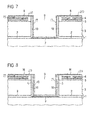
- Figure 7 is a cross section of an intermediate product of an example of the method of producing a semiconductor device with through-substrate via. Elements of the intermediate product according to Figure 7 that correspond to elements of the embodiment according to Figure 1 are designated with the same reference numerals. Figure 7 shows the via layer 6 applied on the upper surface 20, at the sidewall 19 of the via opening 9 and on the connection pad 7.
- Figure 8 is a cross section according to Figure 7 after the removal of the via layer 6 from the upper surface 20 and the application of a further via layer 16, which is applied on the upper surface 20, at the sidewall 19 on the remaining portion of the via layer 6, and above the connection pad 7.
- An interlayer 12, 14 as described above may be applied on the via layer 6 before the further via layer 16 is applied. If a dielectric interlayer 14 is applied, it is removed in an area 17 above the connection pad 7. This may be performed by a spacer etch, which is generally anisotropic but, owing to the large aspect ratio of the relatively deep via opening 9, yields the recessed structure of the dielectric interlayer 14 shown in Figures 5 and 6 with a peripheral portion of the dielectric interlayer 14 remaining above the connection pad 7.
- the conductor layer that is now present on the upper surface 20 is formed by the further via layer 16 only, which is sufficiently thin to prevent an undesired wafer bow.
- the further via layer 16 is then also removed from the upper surface 20. If an interlayer 12, 14 had been provided, it is also removed from the upper surface 20 in this step.
- Figure 9 is a cross section according to Figure 8 after the application of an upper via layer 26 on the upper surface 20, at the sidewall 19 on the remaining portions of the via layer 6 and the further via layer 16 and above the connection pad 7.
- An interlayer 13, 14 as described above may be applied on the further via layer 16 before the upper via layer 26 is applied. If a further dielectric interlayer 14 is applied, it is removed in an area 17 above the connection pad 7. This may be performed by a spacer etch as described above.
- the upper via layer 26, together with an interlayer 12, 14, if provided, may then be removed from the upper surface 20.
- the described method a sequence of any number of electrically conductive via layers and interlayers provided as buffer or stress compensation layers can be produced to obtain the desired good electric conductivity of the through-substrate via.
- the risk of a strong wafer bow is effectively avoided, because the upper surface 20 is not covered by more than one of the applied via layers during the manufacturing process.
- the upper via layer 26 may be left on the upper surface 20, or it may be removed together with an uppermost interlayer 12, 14, if provided, from the upper surface 20.
- Figure 10 is a cross section according to Figure 9 after the application of a top metal 8 and a first mask 21.
- the upper via layer 26 has been removed from the upper surface 20 before the top metal 8 has been applied.
- the top metal 8 is structured by an etching step according to the structure of the first mask 21.
- Figure 11 is a cross section according to Figure 10 after the structuring of the top metal 8.
- the first mask 21 has already been removed.
- a passivation layer 11 may be applied on top to render the device according to Figure 1 .
- the remaining portion of the structured top metal 8 connects the via layers 6, 16, 26 with a plug 15 of the wiring and/or with other conductors of the semiconductor device.
- the connection pad 7 is electrically connected with a conductor at or near the upper surface 20.
- the connection pad 7 may be connected with external terminals or with conductors that are arranged at the rear side of the substrate 1.
- Figure 12 is a cross section according to Figure 10 for a further embodiment. Elements of the further embodiment according to Figure 12 that correspond to elements of the embodiment according to Figure 10 are designated with the same reference numerals.
- the upper via layer 26 has been left on the upper surface 20, and the top metal 8 has been applied on the upper portion of the upper via layer 26.
- the top metal 8 is structured by an etching step together with the upper portion of the upper via layer 26 according to the structure of a second mask 22. The result of this method step after the removal of the second mask 22 is shown in Figure 2 .
- the remaining portion of the structured top metal 8 connects the via layers 6, 16, 26 with a plug 15 of the wiring and/or with other conductors of the semiconductor device.
- connection pad 7 which may be connected with external terminals or with conductors that are arranged at the rear side of the substrate 1, is electrically connected with a conductor at or near the upper surface 20.
- the top metal 8 is optional, and the portion of the upper via layer 26 remaining on the upper surface 20 may suffice as an electric conductor without the top metal 8 being applied.
- the described formation of stress-buffered multiple conductive layers for through-substrate vias comprises subsequent etching steps to remove the succeeding conductive layers from the planar substrate surface while leaving the sidewall and the bottom of the open via unetched.
- Particle collisions in which ions at the bottom of the via opening lose energy are augmented by increasing the pressure during an RIE step (reactive ion etching). This results in the main etch attack being directed to the upper substrate surface.
- RIE step reactive ion etching
- the described method in which the sequence of via layers is produced with intervening etchback steps, solves the problem of keeping the layer stress on the upper surface within tolerable limits while allowing the electric conductivity of the through-substrate via to be optimized.
- the insertion of electrically conductive buffer layers which compensate the stress occurring between the via layers, allows a common structuring of all the via layers by one masked etching step.
- the insertion of dielectric buffer layers is an alternative that is easily feasible, because the dielectric buffer layers can be structured according to a well-known spacer etching, which allows the conductive via layers to be etched back independently outside the via opening.
Landscapes
- Internal Circuitry In Semiconductor Integrated Circuit Devices (AREA)
Abstract
Description
- Semiconductor device with through-substrate via of enhanced conductivity and method of producing a semiconductor device with through-substrate via of enhanced conductivity
- Through-substrate vias provide electric interconnects through a semiconductor layer forming a substrate of a semiconductor device.
-
WO 2012/031845 A1 discloses a through-substrate via provided with a tungsten layer, which forms the electrically conductive track of the via. - A through-substrate via with a width of 80 µm and a depth of 200 µm comprising a tungsten layer as electric conductor typically has a resistance of about 400 mΩ if the thickness of the tungsten layer is 200 nm. In this case the maximum current capability is typically limited to 80 mA. Much higher currents are needed for many applications of semiconductor devices. The resistance of the through-substrate via may be reduced by applying a thicker metal layer or by completely filling the via with electrically conductive material.
- In the paper of K. Lee et al., "Impact of Cu Diffusion from Cu Through-Silicon Via (TSV) on Device Reliability in 3-D LSIs Evaluated by Transient Capacitance Measurement," IRPS 2012, pp. 2B.4.1 to 2B.4.6, problems arising from the contamination of a copper filling of a through-substrate via are discussed.
- The deposition of a thick metal layer on a wafer surface may generate stress that makes the wafer warp. Increasing the thickness of the metal layer also increases the wafer bow, which must stay below about 100 µm to avoid wafer breakage due to robot handling in typical semiconductor processing tools. Consequently, the thickness of a tungsten layer provided as conductor in the through-substrate via must be kept smaller than about 0,8 µm. This limits the electric conductivity to less than 12/Ω, and the minimal resistance is about 83 mΩ, which is much more than desired.
- The wafer bow generated by the deposition of a thick metal layer can be reduced by an etching process, as discussed in the paper of D. H. Triyoso et al., "Progress and challenges of tungsten-filled through-silicon via", IEEE International Conference on Integrated Circuit Design and Technology, ICICDT 2010, pp. 118 to 121.
- For a tungsten layer that is deposited 0,8 µm thick, it has been found that the wafer bow can be reduced from about 90 µm to about 10 µm by a partial removal of the tungsten layer in a subsequent etching step.
-
US 2010/0240214 A1 discloses multi-layer metal structures and a manufacturing process wherein extra process steps of wafer cleaning are skipped in order to obviate problems deriving from stress between two different metal layers that are applied on a planar surface. - It is an object of the present invention to disclose a semiconductor device comprising a through-substrate via of enhanced electric conductivity. It is a further object to disclose a method of producing such a semiconductor device. These objects are achieved with the semiconductor device according to claim 1 and with the method of producing a semiconductor device according to
claim 9. Embodiments and variants derive from the dependent claims. - The semiconductor device comprises a substrate with an upper surface, the substrate including a semiconductor layer, a connection pad below the semiconductor layer opposite the upper surface, a via opening with a sidewall in the semiconductor layer above the connection pad, and an electrically conductive via layer arranged at the sidewall and in contact with the connection pad. An electrically conductive upper via layer is arranged at the sidewall on or above the via layer and is electrically conductively connected to the connection pad.
- An embodiment of the semiconductor device further comprises an interlayer between the via layer and the upper via layer, the interlayer comprising a material that is different from the via layer and from the upper via layer.
- In a further embodiment the via layer and the upper via layer comprise tensile stress and the interlayer comprises compressive stress. Thus the net mechanical stress generated by the layers is reduced, because the stress occurring in the via layers and the stress occurring in the interlayer compensate each other.
- In a further embodiment the via layer and the upper via layer comprise compressive stress and the interlayer comprises tensile stress.
- In a further embodiment the interlayer is electrically conductive.
- In a further embodiment the interlayer is a dielectric layer, which is recessed in an area above the connection pad.
- A further embodiment further comprises an electrically conductive connection liner. The upper via layer is recessed in the area above the connection pad, and the connection liner electrically connects the upper via layer with the via layer and hence with the connection pad.
- In a further embodiment the via layer and the upper via layer comprise a material selected from the group consisting of tungsten, copper, aluminum and electrically conductively doped polysilicon, and the interlayer comprises a material selected from the group consisting of TiN and TaN. This selection of materials has the advantage that the net mechanical stress generated by the layers is reduced, because the stress occurring in the via layers and the stress occurring in the interlayers compensate each other.
- The method of producing a semiconductor device with through-substrate via comprises the steps of providing a substrate having an upper surface, the substrate including a semiconductor layer, arranging a connection pad below the semiconductor layer opposite the upper surface, producing a via opening with a sidewall in the semiconductor layer above the connection pad, and arranging an electrically conductive via layer on the upper surface, at the sidewall and in contact with the connection pad. The via layer is removed from the upper surface, and an electrically conductive further via layer is arranged on the upper surface and at the sidewall on or above the via layer and is electrically conductively connected to the via layer.
- In a variant of the method, an electrically conductive first interlayer is arranged on the via layer before the further via layer is applied, the first interlayer comprising a material that is different from the via layer.
- In a further variant of the method, an electrically conductive second interlayer is arranged on the further via layer, the second interlayer comprising a material that is different from the further via layer. At least one electrically conductive upper via layer is arranged on the upper surface and at the sidewall, the upper via layer being electrically conductively connected to the via layer.
- In a further variant of the method, a dielectric interlayer is arranged on the via layer before the further via layer is applied, the dielectric interlayer is removed from an area above the connection pad, and the further via layer is subsequently applied.
- In a further variant of the method, the further via layer is arranged so that it is in contact with the via layer in the area above the connection pad.
- In a further variant of the method, the further via layer is removed from the area above the connection pad. An electrically conductive connection liner is applied, which electrically connects the further via layer with the via layer.
- The following is a detailed description of examples of the semiconductor device and of the method in conjunction with the appended figures.
- Figure 1
- is a cross section of an embodiment of the semiconductor device.
- Figure 2
- is a cross section of a further embodiment of the semiconductor device.
- Figure 3
- is a detail of
Figure 2 showing the layer sequence of the through-substrate via. - Figure 4
- is a detail according to
Figure 3 for an embodiment comprising conductive interlayers. - Figure 5
- is a detail according to
Figure 3 for an embodiment comprising a dielectric interlayer. - Figure 6
- is a detail according to
Figure 5 for a further embodiment comprising a dielectric interlayer. - Figure 7
- is a cross section of an intermediate product of an example of the method.
- Figure 8
- is a cross section according to
Figure 7 after the application of a further via layer. - Figure 9
- is a cross section according to
Figure 8 after the application of an upper via layer. - Figure 10
- is a cross section according to
Figure 9 after the application of a mask. - Figure 11
- is a cross section according to
Figure 10 after the structuring of a top metal. - Figure 12
- is a cross section according to
Figure 10 for a further embodiment. -
Figure 1 is a cross section of an embodiment of the semiconductor device comprising a substrate 1 having anupper surface 20. The substrate 1 comprises asemiconductor layer 3, which may be a silicon wafer or part of a silicon wafer, for instance. The substrate 1 may also include anintermetal dielectric 4, in whichstructured metallization planes 5 of a wiring are embedded. Theintermetal dielectric 4 can be arranged on or above thesemiconductor layer 3 and forms theupper surface 20 in this embodiment. Afurther dielectric layer 2 can be arranged on the side of thesemiconductor layer 3 opposite to theupper surface 20. Aconnection pad 7 is arranged below thesemiconductor layer 3 and may preferably be embedded in thedielectric layer 2. A viaopening 9 with asidewall 19 is formed in thesemiconductor layer 3 to provide a through-substrate via. - The electric conductor of the through-substrate via is formed by a sequence of electrically conductive via layers, whose number is at least two and may be three or more. In the embodiment according to
Figure 1 , the electrically conductive via layers comprise a vialayer 6, a further vialayer 16 and an upper vialayer 26. Interlayers may be provided between the via layers, which is described below. The vialayer 6 is preferably insulated from the semiconductor material of thesemiconductor layer 3. This insulation may be provided by adielectric layer 10 arranged at thesidewall 19 of the viaopening 9. In embodiments in which the vialayers upper surface 20, as in the embodiment according toFigure 1 , atop metal 8 may be provided to connect the via layers 6, 16, 26 with further conductors that are arranged in the region of theupper surface 20. The further conductors may include the wiring, in particular a vertical connection plug 15 of the wiring, which is shown inFigure 1 by way of example. Apassivation layer 11 may be applied to cover and protect thetop metal 8 and theupper surface 20. -
Figure 2 is a cross section of a further embodiment. Elements of the further embodiment according toFigure 2 that correspond to elements of the embodiment according toFigure 1 are designated with the same reference numerals. In the embodiment according toFigure 2 , the substrate 1 is structured like an SOI substrate (silicon on insulator substrate). Thedielectric layer 2 is arranged in the substrate 1 between a semiconductor body 3' and thesemiconductor layer 3. In the embodiment according toFigure 2 , a portion of the upper vialayer 26 is present on theupper surface 20 and may be structured according to thetop metal 8. Thetop metal 8 is optional and is not necessary if the resistance of the upper vialayer 26 is sufficiently low. As the upper vialayer 26 is sufficiently thin, the portion of the upper vialayer 26 remaining on theupper surface 20 does not generate a stress bending the substrate 1 more than tolerably. The sequence of vialayers opening 9 renders the resistance of the through-substrate via sufficiently low. The number of electrically conductive vialayers Figure 2 or may be different from three. -
Figure 3 is a detail ofFigure 2 showing the layer sequence of the through-substrate via including the basic vialayer 6, a further vialayer 16 and a third via layer, which is the upper vialayer 26 in this embodiment. The number of electrically conductive vialayers Figure 3 , is at least two and may be larger than three. Thesidewall 19 of the viaopening 9 is formed by thedielectric layer 10 insulating the vialayer 6 from thesemiconductor layer 3. The electrically conductive vialayer 6 is in electric contact with theconnection pad 7. The via layers 6, 16, 26 may comprise any electrically conductive material used in semiconductor technology like tungsten, copper, aluminum, electrically conductively doped polysilicon or combinations thereof, for instance. The via layers 6, 16, 26 may comprise different electrically conductive materials or may instead all be formed from the same material. -
Figure 4 is a detail according toFigure 3 for an embodiment comprising electricallyconductive interlayers layers layers first interlayer 12, which may be a liner formed from TiN or TaN, for instance, is arranged between the vialayer 6 and the further vialayer 16. Asecond interlayer 13, which may also be a liner of TiN or TaN, for instance, is arranged between the further vialayer 16 and the upper vialayer 26. If there is another number of via layers, the number of interlayers may differ accordingly. Interlayers may be provided between each pair of subsequent via layers or may only be provided between some of the via layers. Theinterlayers interlayers Figure 4 , the electric conductivity of the through-substrate via is not essentially affected by the presence of theinterlayers -
Figure 5 is a detail according toFigure 3 for an embodiment comprising adielectric interlayer 14 between the vialayer 6 and the further vialayer 16. The number of electrically conductive vialayers Figure 5 , is at least two and may be larger than three. Thedielectric interlayer 14 may be SiO2, for instance. Thedielectric interlayer 14 is recessed in anarea 17 above theconnection pad 7. In thisarea 17 the further vialayer 16 is directly applied on the vialayer 6, so that the vialayer 6 and the further vialayer 16 are electrically conductively connected to one another. A further recessed dielectric interlayer, which is not shown inFigure 5 , may be arranged between the further vialayer 16 and the upper vialayer 26.Dielectric interlayers 14 may be provided between each pair of subsequent via layers or may only be provided between a selected number of via layers. Thedielectric interlayers 14 may be provided as buffer layers to reduce stress that may occur between the via layers 6, 16, 26. Recesses of thedielectric interlayers 14 in thearea 17 above theconnection pad 7 allow the via layers 6, 16, 26 to be electrically conductively connected to one another. In further embodiments,dielectric interlayers 14 and electricallyconductive interlayers Figure 4 may be combined or alternatively applied between the via layers 6, 16, 26. -
Figure 6 is a detail according toFigure 5 for a further embodiment comprising adielectric interlayer 14. In the embodiment according toFigure 6 there are only two via layers: the basic vialayer 6 and the upper vialayer 26, which is recessed in thearea 17 above theconnection pad 7. There may be further via layers as in the embodiments described above. An electrically conductive connection between the upper vialayer 26 and the vialayer 6 is provided by an electricallyconductive connection liner 18, which may be TiN or TaN, for instance. If there are further electrically conductive via layers besides the two vialayers Figure 6 , each further vialayer 16 may be recessed in thearea 17 above theconnection pad 7 to allow an electric connection of all the via layers 6, 16, 26 by means of theconnection liner 18.Dielectric interlayers 14 may be provided between each pair of subsequent via layers or may instead only be provided between a selected number of via layers.Dielectric interlayers 14 and electricallyconductive interlayers Figure 4 may be combined or alternatively applied in an embodiment in which the via layers are connected by means of aconnection liner 18. -
Figure 7 is a cross section of an intermediate product of an example of the method of producing a semiconductor device with through-substrate via. Elements of the intermediate product according toFigure 7 that correspond to elements of the embodiment according toFigure 1 are designated with the same reference numerals.Figure 7 shows the vialayer 6 applied on theupper surface 20, at thesidewall 19 of the viaopening 9 and on theconnection pad 7. -
Figure 8 is a cross section according toFigure 7 after the removal of the vialayer 6 from theupper surface 20 and the application of a further vialayer 16, which is applied on theupper surface 20, at thesidewall 19 on the remaining portion of the vialayer 6, and above theconnection pad 7. Aninterlayer layer 6 before the further vialayer 16 is applied. If adielectric interlayer 14 is applied, it is removed in anarea 17 above theconnection pad 7. This may be performed by a spacer etch, which is generally anisotropic but, owing to the large aspect ratio of the relatively deep viaopening 9, yields the recessed structure of thedielectric interlayer 14 shown inFigures 5 and 6 with a peripheral portion of thedielectric interlayer 14 remaining above theconnection pad 7. As the vialayer 6 had been removed from theupper surface 20, the conductor layer that is now present on theupper surface 20 is formed by the further vialayer 16 only, which is sufficiently thin to prevent an undesired wafer bow. The further vialayer 16 is then also removed from theupper surface 20. If aninterlayer upper surface 20 in this step. -
Figure 9 is a cross section according toFigure 8 after the application of an upper vialayer 26 on theupper surface 20, at thesidewall 19 on the remaining portions of the vialayer 6 and the further vialayer 16 and above theconnection pad 7. Aninterlayer layer 16 before the upper vialayer 26 is applied. If a furtherdielectric interlayer 14 is applied, it is removed in anarea 17 above theconnection pad 7. This may be performed by a spacer etch as described above. The upper vialayer 26, together with aninterlayer upper surface 20. - By the described method a sequence of any number of electrically conductive via layers and interlayers provided as buffer or stress compensation layers can be produced to obtain the desired good electric conductivity of the through-substrate via. At the same time the risk of a strong wafer bow is effectively avoided, because the
upper surface 20 is not covered by more than one of the applied via layers during the manufacturing process. After all via layers have been applied, the upper vialayer 26 may be left on theupper surface 20, or it may be removed together with anuppermost interlayer upper surface 20. -
Figure 10 is a cross section according toFigure 9 after the application of atop metal 8 and a first mask 21. In the embodiment shown inFigure 10 , the upper vialayer 26 has been removed from theupper surface 20 before thetop metal 8 has been applied. Thetop metal 8 is structured by an etching step according to the structure of the first mask 21. -
Figure 11 is a cross section according toFigure 10 after the structuring of thetop metal 8. In the state shown inFigure 11 the first mask 21 has already been removed. Apassivation layer 11 may be applied on top to render the device according toFigure 1 . The remaining portion of the structuredtop metal 8 connects the via layers 6, 16, 26 with aplug 15 of the wiring and/or with other conductors of the semiconductor device. In this way theconnection pad 7 is electrically connected with a conductor at or near theupper surface 20. Theconnection pad 7 may be connected with external terminals or with conductors that are arranged at the rear side of the substrate 1. These details are not essential to the invention and hence not shown in the Figures. -
Figure 12 is a cross section according toFigure 10 for a further embodiment. Elements of the further embodiment according toFigure 12 that correspond to elements of the embodiment according toFigure 10 are designated with the same reference numerals. In the embodiment according toFigure 12 the upper vialayer 26 has been left on theupper surface 20, and thetop metal 8 has been applied on the upper portion of the upper vialayer 26. Thetop metal 8 is structured by an etching step together with the upper portion of the upper vialayer 26 according to the structure of asecond mask 22. The result of this method step after the removal of thesecond mask 22 is shown inFigure 2 . The remaining portion of the structuredtop metal 8 connects the via layers 6, 16, 26 with aplug 15 of the wiring and/or with other conductors of the semiconductor device. In this way theconnection pad 7, which may be connected with external terminals or with conductors that are arranged at the rear side of the substrate 1, is electrically connected with a conductor at or near theupper surface 20. In the embodiment according toFigure 2 , thetop metal 8 is optional, and the portion of the upper vialayer 26 remaining on theupper surface 20 may suffice as an electric conductor without thetop metal 8 being applied. - The described formation of stress-buffered multiple conductive layers for through-substrate vias comprises subsequent etching steps to remove the succeeding conductive layers from the planar substrate surface while leaving the sidewall and the bottom of the open via unetched. Particle collisions in which ions at the bottom of the via opening lose energy are augmented by increasing the pressure during an RIE step (reactive ion etching). This results in the main etch attack being directed to the upper substrate surface. This can be achieved with any electrically conductive layers, including tungsten, copper or doped polysilicon layers, for instance.
- The described method, in which the sequence of via layers is produced with intervening etchback steps, solves the problem of keeping the layer stress on the upper surface within tolerable limits while allowing the electric conductivity of the through-substrate via to be optimized. The insertion of electrically conductive buffer layers, which compensate the stress occurring between the via layers, allows a common structuring of all the via layers by one masked etching step. The insertion of dielectric buffer layers is an alternative that is easily feasible, because the dielectric buffer layers can be structured according to a well-known spacer etching, which allows the conductive via layers to be etched back independently outside the via opening.
List of reference numerals 1 substrate 2 dielectric layer 3 semiconductor layer 3' semiconductor body 4 intermetal dielectric 5 metallization plane 6 via layer 7 connection pad 8 top metal 9 via opening 10 dielectric layer 11 passivation layer 12 first interlayer 13 second interlayer 14 dielectric interlayer 15 plug 16 further via layer 17 area above the connection pad 18 connection liner 19 sidewall 20 upper surface 21 first mask 22 second mask 26 upper via layer
Claims (14)
- A semiconductor device with a through-substrate via, comprising:- a substrate (1) with an upper surface (20), the substrate (1) including a semiconductor layer (3),- a connection pad (7) below the semiconductor layer (3) opposite the upper surface (20),- a via opening (9) with a sidewall (19) in the semiconductor layer (3) above the connection pad (7), and- an electrically conductive via layer (6) arranged at the sidewall (19) and in contact with the connection pad (7),
characterized in that- an electrically conductive upper via layer (26) is arranged at the sidewall (19) on or above the via layer (6) and is electrically conductively connected to the connection pad (7). - The semiconductor device of claim 1, further comprising:an interlayer (12, 13, 14) between the via layer (6) andthe upper via layer (26), the interlayer (12, 13, 14) comprising a material that is different from the via layer (6) and from the upper via layer (26).
- The semiconductor device of claim 2, wherein
the via layer (6) and the upper via layer (26) comprise tensile stress and the interlayer (12, 13, 14) comprises compressive stress. - The semiconductor device of claim 2, wherein
the via layer (6) and the upper via layer (26) comprise compressive stress and the interlayer (12, 13, 14) comprises tensile stress. - The semiconductor device of one of claims 2 to 4, wherein
the interlayer (12, 13) is electrically conductive. - The semiconductor device of one of claims 2 to 4, wherein
the interlayer (14) is a dielectric layer, and
the interlayer (14) is recessed in an area (17) above the connection pad (7). - The semiconductor device of claim 6, further comprising:an electrically conductive connection liner (18),the upper via layer (26) being recessed in the area (17) above the connection pad (7), andthe connection liner (18) electrically connecting the upper via layer (26) with the via layer (6).
- The semiconductor device of claim 2, wherein
the via layer (6) and the upper via layer (26) comprise a material selected from the group consisting of tungsten, copper, aluminum and electrically conductively doped polysilicon, and
the interlayer (12, 13) comprises a material selected from the group consisting of TiN and TaN. - A method of producing a semiconductor device with through-substrate via, comprising:- providing a substrate (1) having an upper surface (20), the substrate (1) including a semiconductor layer (3),- arranging a connection pad (7) below the semiconductor layer (3) opposite the upper surface (20),- producing a via opening (9) with a sidewall (19) in the semiconductor layer (3) above the connection pad (7), and- arranging an electrically conductive via layer (6) on the upper surface (20), at the sidewall (19) and in contact with the connection pad (7),
characterized in that- the via layer (6) is removed from the upper surface (20), and- an electrically conductive further via layer (16) is arranged on the upper surface (20) and at the sidewall (19) on or above the via layer (6) and is electrically conductively connected to the via layer (6). - The method of claim 9, further comprising:arranging an electrically conductive first interlayer (12) on the via layer (6) before the further via layer (16) is applied, the first interlayer (12) comprising a material that is different from the via layer (6).
- The method of claim 10, further comprising:arranging an electrically conductive second interlayer (13) on the further via layer (16), the second interlayer (13) comprising a material that is different from the further via layer (16), andarranging at least one electrically conductive upper via layer (26) on the upper surface (20) and at the sidewall (19), the upper via layer (26) being electrically conductively connected to the via layer (6).
- The method of claim 9, further comprising:arranging a dielectric interlayer (14) on the via layer (6) before the further via layer (16) is applied, removing the dielectric interlayer (14) from an area (17) above the connection pad (7), andsubsequently applying the further via layer (16).
- The method of claim 12, wherein
the further via layer (16) is arranged so that it is in contact with the via layer (6) in the area (17) above the connection pad (7). - The method of claim 12, wherein
the further via layer (16) is removed from the area (17) above the connection pad (7), and
an electrically conductive connection liner (18) is applied electrically connecting the further via layer (16) with the via layer (6).
Priority Applications (1)
| Application Number | Priority Date | Filing Date | Title |
|---|---|---|---|
| EP13163968.4A EP2793254B1 (en) | 2013-04-16 | 2013-04-16 | Semiconductor device with through-substrate via of enhanced conductivity and corresponding fabrication method |
Applications Claiming Priority (1)
| Application Number | Priority Date | Filing Date | Title |
|---|---|---|---|
| EP13163968.4A EP2793254B1 (en) | 2013-04-16 | 2013-04-16 | Semiconductor device with through-substrate via of enhanced conductivity and corresponding fabrication method |
Publications (2)
| Publication Number | Publication Date |
|---|---|
| EP2793254A1 true EP2793254A1 (en) | 2014-10-22 |
| EP2793254B1 EP2793254B1 (en) | 2015-10-21 |
Family
ID=48143106
Family Applications (1)
| Application Number | Title | Priority Date | Filing Date |
|---|---|---|---|
| EP13163968.4A Active EP2793254B1 (en) | 2013-04-16 | 2013-04-16 | Semiconductor device with through-substrate via of enhanced conductivity and corresponding fabrication method |
Country Status (1)
| Country | Link |
|---|---|
| EP (1) | EP2793254B1 (en) |
Cited By (2)
| Publication number | Priority date | Publication date | Assignee | Title |
|---|---|---|---|---|
| WO2015185354A3 (en) * | 2014-06-06 | 2016-03-03 | Robert Bosch Gmbh | Semiconductor component having at least one via in the carrier substrate and method for producing such a via |
| CN113053804A (en) * | 2021-03-10 | 2021-06-29 | 中国科学院微电子研究所 | Tungsten composite film layer, growth method thereof and monolithic 3DIC |
Citations (7)
| Publication number | Priority date | Publication date | Assignee | Title |
|---|---|---|---|---|
| US20090174080A1 (en) * | 2005-08-26 | 2009-07-09 | Toshio Saito | Semiconductor device |
| US20100130002A1 (en) * | 2008-11-25 | 2010-05-27 | Dao Thuy B | Multilayered through via |
| US20100240214A1 (en) | 2009-03-20 | 2010-09-23 | Nanya Technology Corp. | Method of forming multi metal layers thin film on wafer |
| US20100308435A1 (en) * | 2009-06-08 | 2010-12-09 | Qualcomm Incorporated | Through Silicon Via With Embedded Decoupling Capacitor |
| US20110079920A1 (en) * | 2009-10-05 | 2011-04-07 | Stmicroelectronics (Crolles 2) Sas | Electrical connection via for the substrate of a semiconductor device |
| WO2012031845A1 (en) | 2010-09-10 | 2012-03-15 | Austriamicrosystems Ag | Method for producing a semiconductor component with a through-contact and semiconductor component with through-contact |
| US8153520B1 (en) * | 2009-08-03 | 2012-04-10 | Novellus Systems, Inc. | Thinning tungsten layer after through silicon via filling |
-
2013
- 2013-04-16 EP EP13163968.4A patent/EP2793254B1/en active Active
Patent Citations (7)
| Publication number | Priority date | Publication date | Assignee | Title |
|---|---|---|---|---|
| US20090174080A1 (en) * | 2005-08-26 | 2009-07-09 | Toshio Saito | Semiconductor device |
| US20100130002A1 (en) * | 2008-11-25 | 2010-05-27 | Dao Thuy B | Multilayered through via |
| US20100240214A1 (en) | 2009-03-20 | 2010-09-23 | Nanya Technology Corp. | Method of forming multi metal layers thin film on wafer |
| US20100308435A1 (en) * | 2009-06-08 | 2010-12-09 | Qualcomm Incorporated | Through Silicon Via With Embedded Decoupling Capacitor |
| US8153520B1 (en) * | 2009-08-03 | 2012-04-10 | Novellus Systems, Inc. | Thinning tungsten layer after through silicon via filling |
| US20110079920A1 (en) * | 2009-10-05 | 2011-04-07 | Stmicroelectronics (Crolles 2) Sas | Electrical connection via for the substrate of a semiconductor device |
| WO2012031845A1 (en) | 2010-09-10 | 2012-03-15 | Austriamicrosystems Ag | Method for producing a semiconductor component with a through-contact and semiconductor component with through-contact |
Non-Patent Citations (2)
| Title |
|---|
| D. H. TRIYOSO ET AL.: "Progress and challenges of tungsten-filled through-silicon via", IEEE INTERNATIONAL CONFERENCE ON INTEGRATED CIRCUIT DESIGN AND TECHNOLOGY, 2010, pages 118 - 121 |
| K. LEE ET AL.: "Impact of Cu Diffusion from Cu Through-Silicon Via (TSV) on Device Reliability in 3-D LSIs Evaluated by Transient Capacitance Measurement", IRPS, 2012, pages 2B.4.1 - 2B.4.6 |
Cited By (3)
| Publication number | Priority date | Publication date | Assignee | Title |
|---|---|---|---|---|
| WO2015185354A3 (en) * | 2014-06-06 | 2016-03-03 | Robert Bosch Gmbh | Semiconductor component having at least one via in the carrier substrate and method for producing such a via |
| CN113053804A (en) * | 2021-03-10 | 2021-06-29 | 中国科学院微电子研究所 | Tungsten composite film layer, growth method thereof and monolithic 3DIC |
| CN113053804B (en) * | 2021-03-10 | 2023-02-21 | 中国科学院微电子研究所 | A kind of tungsten composite film layer and its growth method, monolithic 3DIC |
Also Published As
| Publication number | Publication date |
|---|---|
| EP2793254B1 (en) | 2015-10-21 |
Similar Documents
| Publication | Publication Date | Title |
|---|---|---|
| EP3407376B1 (en) | Semiconductor device and method for manufacturing same | |
| US7560375B2 (en) | Gas dielectric structure forming methods | |
| US9911653B2 (en) | Low capacitance interconnect structures and associated systems and methods | |
| KR102111474B1 (en) | Semiconductor devices having through electrodes and methods for fabricating the same | |
| TWI503981B (en) | Semiconductor device | |
| US20100164062A1 (en) | Method of manufacturing through-silicon-via and through-silicon-via structure | |
| US20140035109A1 (en) | Method and structure of forming backside through silicon via connections | |
| US8679937B2 (en) | Method for fabricating a capacitor and capacitor structure thereof | |
| KR102770256B1 (en) | Devices with through silicon vias, guard rings and methods of making the same | |
| CN101221921B (en) | Semiconductor integrated circuit and its manufacturing method | |
| US10319628B2 (en) | Integrated circuit having a plurality of active layers and method of fabricating the same | |
| US9373536B2 (en) | Stress reduction apparatus | |
| CN102623437A (en) | Through silicon via (TSV) structure and manufacturing method thereof | |
| US8119515B2 (en) | Bonding pad for anti-peeling property and method for fabricating the same | |
| KR20150062626A (en) | Semiconductor devices having through electrodes and methods for fabricating the same | |
| CN112838048B (en) | Interconnect structure and method of making the same | |
| EP2793254B1 (en) | Semiconductor device with through-substrate via of enhanced conductivity and corresponding fabrication method | |
| US20040259358A1 (en) | Self-aligned mask to reduce cell layout area | |
| EP2790211B1 (en) | Method of producing a through-substrate via in a semiconductor device and semiconductor device comprising a through-substrate via | |
| US8691688B2 (en) | Method of manufacturing semiconductor structure | |
| US8772936B2 (en) | Semiconductor device with a copper line and method for manufacturing the same | |
| EP2648214B1 (en) | Methods of producing a semiconductor device with a through-substrate via | |
| KR101113327B1 (en) | Semiconductor device having through via and method of fabricating the same | |
| CN108242386B (en) | Multilayer structure, manufacturing method thereof and contact structure corresponding to multilayer structure | |
| CN104269395A (en) | Low-dielectric constant dielectric etching and copper interconnection structure and integration method |
Legal Events
| Date | Code | Title | Description |
|---|---|---|---|
| PUAI | Public reference made under article 153(3) epc to a published international application that has entered the european phase |
Free format text: ORIGINAL CODE: 0009012 |
|
| 17P | Request for examination filed |
Effective date: 20130416 |
|
| AK | Designated contracting states |
Kind code of ref document: A1 Designated state(s): AL AT BE BG CH CY CZ DE DK EE ES FI FR GB GR HR HU IE IS IT LI LT LU LV MC MK MT NL NO PL PT RO RS SE SI SK SM TR |
|
| AX | Request for extension of the european patent |
Extension state: BA ME |
|
| R17P | Request for examination filed (corrected) |
Effective date: 20150126 |
|
| RBV | Designated contracting states (corrected) |
Designated state(s): AL AT BE BG CH CY CZ DE DK EE ES FI FR GB GR HR HU IE IS IT LI LT LU LV MC MK MT NL NO PL PT RO RS SE SI SK SM TR |
|
| GRAP | Despatch of communication of intention to grant a patent |
Free format text: ORIGINAL CODE: EPIDOSNIGR1 |
|
| INTG | Intention to grant announced |
Effective date: 20150529 |
|
| GRAS | Grant fee paid |
Free format text: ORIGINAL CODE: EPIDOSNIGR3 |
|
| GRAA | (expected) grant |
Free format text: ORIGINAL CODE: 0009210 |
|
| AK | Designated contracting states |
Kind code of ref document: B1 Designated state(s): AL AT BE BG CH CY CZ DE DK EE ES FI FR GB GR HR HU IE IS IT LI LT LU LV MC MK MT NL NO PL PT RO RS SE SI SK SM TR |
|
| REG | Reference to a national code |
Ref country code: GB Ref legal event code: FG4D Ref country code: NL Ref legal event code: MP Effective date: 20151021 |
|
| REG | Reference to a national code |
Ref country code: CH Ref legal event code: EP |
|
| REG | Reference to a national code |
Ref country code: AT Ref legal event code: REF Ref document number: 757081 Country of ref document: AT Kind code of ref document: T Effective date: 20151115 |
|
| REG | Reference to a national code |
Ref country code: IE Ref legal event code: FG4D |
|
| REG | Reference to a national code |
Ref country code: DE Ref legal event code: R096 Ref document number: 602013003515 Country of ref document: DE |
|
| REG | Reference to a national code |
Ref country code: LT Ref legal event code: MG4D |
|
| REG | Reference to a national code |
Ref country code: AT Ref legal event code: MK05 Ref document number: 757081 Country of ref document: AT Kind code of ref document: T Effective date: 20151021 |
|
| PG25 | Lapsed in a contracting state [announced via postgrant information from national office to epo] |
Ref country code: NL Free format text: LAPSE BECAUSE OF FAILURE TO SUBMIT A TRANSLATION OF THE DESCRIPTION OR TO PAY THE FEE WITHIN THE PRESCRIBED TIME-LIMIT Effective date: 20151021 Ref country code: NO Free format text: LAPSE BECAUSE OF FAILURE TO SUBMIT A TRANSLATION OF THE DESCRIPTION OR TO PAY THE FEE WITHIN THE PRESCRIBED TIME-LIMIT Effective date: 20160121 Ref country code: ES Free format text: LAPSE BECAUSE OF FAILURE TO SUBMIT A TRANSLATION OF THE DESCRIPTION OR TO PAY THE FEE WITHIN THE PRESCRIBED TIME-LIMIT Effective date: 20151021 Ref country code: IT Free format text: LAPSE BECAUSE OF FAILURE TO SUBMIT A TRANSLATION OF THE DESCRIPTION OR TO PAY THE FEE WITHIN THE PRESCRIBED TIME-LIMIT Effective date: 20151021 Ref country code: LT Free format text: LAPSE BECAUSE OF FAILURE TO SUBMIT A TRANSLATION OF THE DESCRIPTION OR TO PAY THE FEE WITHIN THE PRESCRIBED TIME-LIMIT Effective date: 20151021 Ref country code: HR Free format text: LAPSE BECAUSE OF FAILURE TO SUBMIT A TRANSLATION OF THE DESCRIPTION OR TO PAY THE FEE WITHIN THE PRESCRIBED TIME-LIMIT Effective date: 20151021 Ref country code: IS Free format text: LAPSE BECAUSE OF FAILURE TO SUBMIT A TRANSLATION OF THE DESCRIPTION OR TO PAY THE FEE WITHIN THE PRESCRIBED TIME-LIMIT Effective date: 20160221 |
|
| PG25 | Lapsed in a contracting state [announced via postgrant information from national office to epo] |
Ref country code: FI Free format text: LAPSE BECAUSE OF FAILURE TO SUBMIT A TRANSLATION OF THE DESCRIPTION OR TO PAY THE FEE WITHIN THE PRESCRIBED TIME-LIMIT Effective date: 20151021 Ref country code: GR Free format text: LAPSE BECAUSE OF FAILURE TO SUBMIT A TRANSLATION OF THE DESCRIPTION OR TO PAY THE FEE WITHIN THE PRESCRIBED TIME-LIMIT Effective date: 20160122 Ref country code: LV Free format text: LAPSE BECAUSE OF FAILURE TO SUBMIT A TRANSLATION OF THE DESCRIPTION OR TO PAY THE FEE WITHIN THE PRESCRIBED TIME-LIMIT Effective date: 20151021 Ref country code: SE Free format text: LAPSE BECAUSE OF FAILURE TO SUBMIT A TRANSLATION OF THE DESCRIPTION OR TO PAY THE FEE WITHIN THE PRESCRIBED TIME-LIMIT Effective date: 20151021 Ref country code: AT Free format text: LAPSE BECAUSE OF FAILURE TO SUBMIT A TRANSLATION OF THE DESCRIPTION OR TO PAY THE FEE WITHIN THE PRESCRIBED TIME-LIMIT Effective date: 20151021 Ref country code: PL Free format text: LAPSE BECAUSE OF FAILURE TO SUBMIT A TRANSLATION OF THE DESCRIPTION OR TO PAY THE FEE WITHIN THE PRESCRIBED TIME-LIMIT Effective date: 20151021 Ref country code: RS Free format text: LAPSE BECAUSE OF FAILURE TO SUBMIT A TRANSLATION OF THE DESCRIPTION OR TO PAY THE FEE WITHIN THE PRESCRIBED TIME-LIMIT Effective date: 20151021 Ref country code: PT Free format text: LAPSE BECAUSE OF FAILURE TO SUBMIT A TRANSLATION OF THE DESCRIPTION OR TO PAY THE FEE WITHIN THE PRESCRIBED TIME-LIMIT Effective date: 20160222 |
|
| REG | Reference to a national code |
Ref country code: DE Ref legal event code: R097 Ref document number: 602013003515 Country of ref document: DE |
|
| PG25 | Lapsed in a contracting state [announced via postgrant information from national office to epo] |
Ref country code: CZ Free format text: LAPSE BECAUSE OF FAILURE TO SUBMIT A TRANSLATION OF THE DESCRIPTION OR TO PAY THE FEE WITHIN THE PRESCRIBED TIME-LIMIT Effective date: 20151021 |
|
| PLBE | No opposition filed within time limit |
Free format text: ORIGINAL CODE: 0009261 |
|
| STAA | Information on the status of an ep patent application or granted ep patent |
Free format text: STATUS: NO OPPOSITION FILED WITHIN TIME LIMIT |
|
| PG25 | Lapsed in a contracting state [announced via postgrant information from national office to epo] |
Ref country code: SM Free format text: LAPSE BECAUSE OF FAILURE TO SUBMIT A TRANSLATION OF THE DESCRIPTION OR TO PAY THE FEE WITHIN THE PRESCRIBED TIME-LIMIT Effective date: 20151021 Ref country code: EE Free format text: LAPSE BECAUSE OF FAILURE TO SUBMIT A TRANSLATION OF THE DESCRIPTION OR TO PAY THE FEE WITHIN THE PRESCRIBED TIME-LIMIT Effective date: 20151021 Ref country code: BE Free format text: LAPSE BECAUSE OF NON-PAYMENT OF DUE FEES Effective date: 20160430 Ref country code: SK Free format text: LAPSE BECAUSE OF FAILURE TO SUBMIT A TRANSLATION OF THE DESCRIPTION OR TO PAY THE FEE WITHIN THE PRESCRIBED TIME-LIMIT Effective date: 20151021 Ref country code: RO Free format text: LAPSE BECAUSE OF FAILURE TO SUBMIT A TRANSLATION OF THE DESCRIPTION OR TO PAY THE FEE WITHIN THE PRESCRIBED TIME-LIMIT Effective date: 20151021 Ref country code: DK Free format text: LAPSE BECAUSE OF FAILURE TO SUBMIT A TRANSLATION OF THE DESCRIPTION OR TO PAY THE FEE WITHIN THE PRESCRIBED TIME-LIMIT Effective date: 20151021 |
|
| 26N | No opposition filed |
Effective date: 20160722 |
|
| PG25 | Lapsed in a contracting state [announced via postgrant information from national office to epo] |
Ref country code: SI Free format text: LAPSE BECAUSE OF FAILURE TO SUBMIT A TRANSLATION OF THE DESCRIPTION OR TO PAY THE FEE WITHIN THE PRESCRIBED TIME-LIMIT Effective date: 20151021 |
|
| REG | Reference to a national code |
Ref country code: CH Ref legal event code: PL |
|
| PG25 | Lapsed in a contracting state [announced via postgrant information from national office to epo] |
Ref country code: LU Free format text: LAPSE BECAUSE OF FAILURE TO SUBMIT A TRANSLATION OF THE DESCRIPTION OR TO PAY THE FEE WITHIN THE PRESCRIBED TIME-LIMIT Effective date: 20160416 Ref country code: BE Free format text: LAPSE BECAUSE OF FAILURE TO SUBMIT A TRANSLATION OF THE DESCRIPTION OR TO PAY THE FEE WITHIN THE PRESCRIBED TIME-LIMIT Effective date: 20151021 |
|
| REG | Reference to a national code |
Ref country code: IE Ref legal event code: MM4A |
|
| REG | Reference to a national code |
Ref country code: FR Ref legal event code: ST Effective date: 20161230 |
|
| PG25 | Lapsed in a contracting state [announced via postgrant information from national office to epo] |
Ref country code: FR Free format text: LAPSE BECAUSE OF NON-PAYMENT OF DUE FEES Effective date: 20160502 Ref country code: LI Free format text: LAPSE BECAUSE OF NON-PAYMENT OF DUE FEES Effective date: 20160430 Ref country code: CH Free format text: LAPSE BECAUSE OF NON-PAYMENT OF DUE FEES Effective date: 20160430 |
|
| PG25 | Lapsed in a contracting state [announced via postgrant information from national office to epo] |
Ref country code: IE Free format text: LAPSE BECAUSE OF NON-PAYMENT OF DUE FEES Effective date: 20160416 |
|
| GBPC | Gb: european patent ceased through non-payment of renewal fee |
Effective date: 20170416 |
|
| PG25 | Lapsed in a contracting state [announced via postgrant information from national office to epo] |
Ref country code: GB Free format text: LAPSE BECAUSE OF NON-PAYMENT OF DUE FEES Effective date: 20170416 |
|
| PG25 | Lapsed in a contracting state [announced via postgrant information from national office to epo] |
Ref country code: HU Free format text: LAPSE BECAUSE OF FAILURE TO SUBMIT A TRANSLATION OF THE DESCRIPTION OR TO PAY THE FEE WITHIN THE PRESCRIBED TIME-LIMIT; INVALID AB INITIO Effective date: 20130416 |
|
| PG25 | Lapsed in a contracting state [announced via postgrant information from national office to epo] |
Ref country code: CY Free format text: LAPSE BECAUSE OF FAILURE TO SUBMIT A TRANSLATION OF THE DESCRIPTION OR TO PAY THE FEE WITHIN THE PRESCRIBED TIME-LIMIT Effective date: 20151021 Ref country code: MK Free format text: LAPSE BECAUSE OF FAILURE TO SUBMIT A TRANSLATION OF THE DESCRIPTION OR TO PAY THE FEE WITHIN THE PRESCRIBED TIME-LIMIT Effective date: 20151021 Ref country code: MT Free format text: LAPSE BECAUSE OF NON-PAYMENT OF DUE FEES Effective date: 20160430 Ref country code: MC Free format text: LAPSE BECAUSE OF FAILURE TO SUBMIT A TRANSLATION OF THE DESCRIPTION OR TO PAY THE FEE WITHIN THE PRESCRIBED TIME-LIMIT Effective date: 20151021 |
|
| PG25 | Lapsed in a contracting state [announced via postgrant information from national office to epo] |
Ref country code: BG Free format text: LAPSE BECAUSE OF FAILURE TO SUBMIT A TRANSLATION OF THE DESCRIPTION OR TO PAY THE FEE WITHIN THE PRESCRIBED TIME-LIMIT Effective date: 20151021 |
|
| PG25 | Lapsed in a contracting state [announced via postgrant information from national office to epo] |
Ref country code: TR Free format text: LAPSE BECAUSE OF FAILURE TO SUBMIT A TRANSLATION OF THE DESCRIPTION OR TO PAY THE FEE WITHIN THE PRESCRIBED TIME-LIMIT Effective date: 20151021 Ref country code: AL Free format text: LAPSE BECAUSE OF FAILURE TO SUBMIT A TRANSLATION OF THE DESCRIPTION OR TO PAY THE FEE WITHIN THE PRESCRIBED TIME-LIMIT Effective date: 20151021 |
|
| P01 | Opt-out of the competence of the unified patent court (upc) registered |
Effective date: 20230822 |
|
| REG | Reference to a national code |
Ref country code: DE Ref legal event code: R079 Ref document number: 602013003515 Country of ref document: DE Free format text: PREVIOUS MAIN CLASS: H01L0021768000 Ipc: H10W0020000000 |
|
| REG | Reference to a national code |
Ref country code: DE Ref legal event code: R081 Ref document number: 602013003515 Country of ref document: DE Owner name: AMS-OSRAM AG, AT Free format text: FORMER OWNER: AMS AG, UNTERPREMSTAETTEN, AT |
|
| PGFP | Annual fee paid to national office [announced via postgrant information from national office to epo] |
Ref country code: DE Payment date: 20260422 Year of fee payment: 14 |