EP2793083A1 - Holder, lithography apparatus, and method of manufacturing article - Google Patents
Holder, lithography apparatus, and method of manufacturing article Download PDFInfo
- Publication number
- EP2793083A1 EP2793083A1 EP20140162005 EP14162005A EP2793083A1 EP 2793083 A1 EP2793083 A1 EP 2793083A1 EP 20140162005 EP20140162005 EP 20140162005 EP 14162005 A EP14162005 A EP 14162005A EP 2793083 A1 EP2793083 A1 EP 2793083A1
- Authority
- EP
- European Patent Office
- Prior art keywords
- substrate
- holder
- base
- holding portion
- pins
- Prior art date
- Legal status (The legal status is an assumption and is not a legal conclusion. Google has not performed a legal analysis and makes no representation as to the accuracy of the status listed.)
- Granted
Links
Images


Classifications
-
- G—PHYSICS
- G03—PHOTOGRAPHY; CINEMATOGRAPHY; ANALOGOUS TECHNIQUES USING WAVES OTHER THAN OPTICAL WAVES; ELECTROGRAPHY; HOLOGRAPHY
- G03F—PHOTOMECHANICAL PRODUCTION OF TEXTURED OR PATTERNED SURFACES, e.g. FOR PRINTING, FOR PROCESSING OF SEMICONDUCTOR DEVICES; MATERIALS THEREFOR; ORIGINALS THEREFOR; APPARATUS SPECIALLY ADAPTED THEREFOR
- G03F7/00—Photomechanical, e.g. photolithographic, production of textured or patterned surfaces, e.g. printing surfaces; Materials therefor, e.g. comprising photoresists; Apparatus specially adapted therefor
- G03F7/20—Exposure; Apparatus therefor
-
- B—PERFORMING OPERATIONS; TRANSPORTING
- B25—HAND TOOLS; PORTABLE POWER-DRIVEN TOOLS; MANIPULATORS
- B25B—TOOLS OR BENCH DEVICES NOT OTHERWISE PROVIDED FOR, FOR FASTENING, CONNECTING, DISENGAGING, OR HOLDING
- B25B11/00—Work holders not covered by any preceding group in the subclass, e.g. magnetic work holders, vacuum work holders
- B25B11/005—Vacuum work holders
-
- G—PHYSICS
- G03—PHOTOGRAPHY; CINEMATOGRAPHY; ANALOGOUS TECHNIQUES USING WAVES OTHER THAN OPTICAL WAVES; ELECTROGRAPHY; HOLOGRAPHY
- G03F—PHOTOMECHANICAL PRODUCTION OF TEXTURED OR PATTERNED SURFACES, e.g. FOR PRINTING, FOR PROCESSING OF SEMICONDUCTOR DEVICES; MATERIALS THEREFOR; ORIGINALS THEREFOR; APPARATUS SPECIALLY ADAPTED THEREFOR
- G03F7/00—Photomechanical, e.g. photolithographic, production of textured or patterned surfaces, e.g. printing surfaces; Materials therefor, e.g. comprising photoresists; Apparatus specially adapted therefor
- G03F7/70—Microphotolithographic exposure; Apparatus therefor
- G03F7/70691—Handling of masks or workpieces
- G03F7/707—Chucks, e.g. chucking or un-chucking operations or structural details
-
- G—PHYSICS
- G03—PHOTOGRAPHY; CINEMATOGRAPHY; ANALOGOUS TECHNIQUES USING WAVES OTHER THAN OPTICAL WAVES; ELECTROGRAPHY; HOLOGRAPHY
- G03F—PHOTOMECHANICAL PRODUCTION OF TEXTURED OR PATTERNED SURFACES, e.g. FOR PRINTING, FOR PROCESSING OF SEMICONDUCTOR DEVICES; MATERIALS THEREFOR; ORIGINALS THEREFOR; APPARATUS SPECIALLY ADAPTED THEREFOR
- G03F7/00—Photomechanical, e.g. photolithographic, production of textured or patterned surfaces, e.g. printing surfaces; Materials therefor, e.g. comprising photoresists; Apparatus specially adapted therefor
- G03F7/70—Microphotolithographic exposure; Apparatus therefor
- G03F7/70691—Handling of masks or workpieces
- G03F7/70716—Stages
-
- H—ELECTRICITY
- H10—SEMICONDUCTOR DEVICES; ELECTRIC SOLID-STATE DEVICES NOT OTHERWISE PROVIDED FOR
- H10P—GENERIC PROCESSES OR APPARATUS FOR THE MANUFACTURE OR TREATMENT OF DEVICES COVERED BY CLASS H10
- H10P72/00—Handling or holding of wafers, substrates or devices during manufacture or treatment thereof
- H10P72/70—Handling or holding of wafers, substrates or devices during manufacture or treatment thereof for supporting or gripping
- H10P72/76—Handling or holding of wafers, substrates or devices during manufacture or treatment thereof for supporting or gripping using mechanical means, e.g. clamps or pinches
- H10P72/7604—Handling or holding of wafers, substrates or devices during manufacture or treatment thereof for supporting or gripping using mechanical means, e.g. clamps or pinches the wafers being placed on a susceptor, stage or support
- H10P72/7614—Handling or holding of wafers, substrates or devices during manufacture or treatment thereof for supporting or gripping using mechanical means, e.g. clamps or pinches the wafers being placed on a susceptor, stage or support characterised by a plurality of individual support members, e.g. support posts or protrusions
-
- H—ELECTRICITY
- H10—SEMICONDUCTOR DEVICES; ELECTRIC SOLID-STATE DEVICES NOT OTHERWISE PROVIDED FOR
- H10P—GENERIC PROCESSES OR APPARATUS FOR THE MANUFACTURE OR TREATMENT OF DEVICES COVERED BY CLASS H10
- H10P72/00—Handling or holding of wafers, substrates or devices during manufacture or treatment thereof
- H10P72/70—Handling or holding of wafers, substrates or devices during manufacture or treatment thereof for supporting or gripping
- H10P72/78—Handling or holding of wafers, substrates or devices during manufacture or treatment thereof for supporting or gripping using vacuum or suction, e.g. Bernoulli chucks
Definitions
- the present invention relates to a holder, a lithography apparatus, and a method of manufacturing an article.
- NA numerical aperture
- the throughput of the exposure apparatus is enhanced and, for example, there is a need for a stage for holding a substrate which increases the acceleration.
- One method of implementing the high acceleration of the stage is to reduce the weight of the stage, and attempt to reduce the weight of a holder (chuck) that chucks and holds a substrate have been made.
- the present invention provides, for example, a holder which enhances the flatness of a substrate held thereby.
- Fig. 1 is a schematic view showing the arrangement of a lithography apparatus 1 according to an aspect of the present invention.
- the lithography apparatus 1 is an apparatus that forms (transfers) a pattern onto a substrate.
- the lithography apparatus 1 is embodied as an exposure apparatus that exposes a substrate via a projection optical system and forms a pattern on the substrate.
- the lithography apparatus 1 is not limited to the exposure apparatus.
- the lithography apparatus 1 may be a drawing apparatus that draws and forms a pattern on a substrate using a charged particle beam (for example, electron beam or ion beam) via a charged particle optical system.
- the lithography apparatus 1 may be an imprint apparatus that molds an imprint material (for example, resin) on a substrate using a mold and forms a pattern on the substrate.
- the lithography apparatus 1 includes an illumination optical system 102, a reticle stage (not shown) that hold a reticle 104, a projection optical system 106, and a substrate stage 110 that holds a substrate 108.
- the substrate stage 110 is a holding apparatus that can move while holding the substrate 108, and includes a holder (chuck) 112 and a stage table 114 on which the holder 112 is placed. Detailed arrangements of the substrate stage 110 will be described below in the respective embodiments.
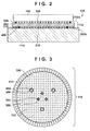
- Figs. 2 and 3 are views showing the arrangement of a substrate stage 110 according to the first embodiment of the present invention.
- Fig. 2 is a sectional view of the substrate stage 110
- Fig. 3 is a plan view of the second surface of a holder 112 of the substrate stage 110.
- the holder 112 includes a base 202 that is made of a material having a high thermal conductivity, for example, SiC ceramic, and includes a first surface (front surface) 202a on the substrate side and a second surface (back surface) 202b on the side opposite to the first surface 202a.
- the base 202 has one or a plurality of substrate vacuum holes 302 as through holes extending through the base 202.
- a stage table 114 has substrate vacuum holes communicating with the substrate vacuum holes 302, which are connected to a vacuum source (not shown).
- the stage table 114 also has holder vacuum holes configured to chuck the holder 112, which are connected to a vacuum source (not shown).
- lift pins pins that chuck the substrate 108 and move up and down relative to the stage table 114) for transfer of the substrate 108 are necessary.
- lift pin holes 304 having a diameter larger than that of the lift pins are formed in the base 202 as through holes extending through the base 202.
- Circumferential first holding portions (not shown) that surround the lift pin holes 304 through the perimeter and a circumferential second holding portion 204 that surrounds the first holding portions are formed on the first surface 202a of the base 202 to chuck (hold) the substrate 108.
- the second holding portion 204 seals the space between the substrate 108 and the first surface 202a of the base 202.
- the first holding portions and the second holding portion 204 contact the substrate 108 and define a substrate holding plane that holds the substrate 108.
- the second holding portion 204 is formed in a region of the first surface 202a between the outer edge of the base 202 and a projection region where a second support portion 208 formed on the second surface 202b of the base 202 is projected to the first surface 202a of the base 202.
- the second holding portion 204 is formed between the outer edge of the base 202 and the region of the first surface 202a above the second support portion 208.
- the second holding portion 204 is the member formed at the outermost position out of the members that are formed on the first surface 202a of the base 202 and contact the substrate 108.
- the second holding portion 204 is formed to have a diameter smaller than that of the substrate 108.
- a plurality of pins (pin-shaped projections) 206 that contact the substrate 108 are formed in the region of the first surface 202a surrounded by the second holding portion 204, more specifically, in the region of the first surface 202a between the second holding portion 204 and the first holding portions.
- the plurality of pins 206 also define the substrate holding plane that holds the substrate 108 together with the first holding portions and the second holding portion 204.
- the first holding portions, the second holding portion 204, and the pins 206 thus define the substrate holding plane. This makes it possible to hold the substrate 108 while maintaining a high flatness when vacuum-chucking the substrate 108.
- Circumferential support portions 306 that surround the lift pin holes 304 through the perimeter and circumferential support portions 308 that surround the substrate vacuum holes 302 through the perimeter are formed on the second surface 202b of the base 202 to chuck (hold) the substrate 108.
- the support portions 306 and 308 constitute first support portions that surround the through holes extending through the base 202 through the perimeter.
- the circumferential second support portion 208 is also formed on the second surface 202b of the base 202 so as to surround the support portions 306 and 308 as the first support portions.
- the support portions 306 and 308 and the second support portion 208 contact the stage table 114.
- a plurality of pins (pin-shaped projections) 210 that contact the stage table 114 are formed in the region of the second surface 202b surrounded by the second support portion 208, more specifically, in the region of the second surface 202b between the second support portion 208 and the support portions 306 and 308 (first support portions).
- the support portions 306 and 308 and the second support portion 208 thus contact the stage table 114. This makes it possible to maintain the flatness of the holder 112 when vacuum-chucking the substrate 108 or the holder 112.
- a plurality of second surface-side pins 212 that contact the stage table 114 are formed outside the second support portion 208, that is, in the region of the second surface 202b between the outer edge of the base 202 and the second support portion 208.
- Figs. 4 and 5 are views showing the arrangement of a substrate stage 110 according to the second embodiment of the present invention.
- Fig. 4 is a sectional view of the substrate stage 110
- Fig. 5 is a plan view of the second surface of a holder 112 of the substrate stage 110.
- a plurality of first surface-side pins 214 that contact a substrate 108 are formed outside a second holding portion 204, that is, in the region of a first surface 202a between the second holding portion 204 and the outer edge of a base 202, in addition to the features described in the first embodiment.
- the second holding portion 204 overlaps a projection region where a second support portion 208 is projected from the second surface side to the first surface side of the base 202.
- the second holding portion 204 is formed so as to at least partially overlap the second support portion 208 on the second support portion 208.
- the second holding portion 204 is formed so as to fit within the second support portion 208 (not to lie off the second support portion 208) on the second support portion 208.
- the width of the second holding portion 204 is smaller than that of the second support portion 208.
- the first surface-side pins 214 overlap projection regions where second surface-side pins 212 are projected from the second surface side to the first surface side of the base 202.
- each of the first surface-side pins 214 is formed so as to at least partially overlap a corresponding one of the second surface-side pins 212 on the second surface-side pin.
- each of the first surface-side pins 214 is formed so as to fit within a corresponding one of the second surface-side pins 212 (not to lie off the one second surface-side pin) on the second surface-side pin.
- the width of the first surface-side pin 214 is smaller than that of the second surface-side pin 212.
- the second support portion 208 can be formed on the second surface 202b of the base 202 on the outer side as compared to the first embodiment. It is therefore possible to suppress flexture of the outer edge portion of the holder 112 caused by making the holder 112 thinner and further reduce deformation of the holder 112.
- the second surface-side pins 212 that are formed outside the second support portion 208 contact a stage table 114, and additionally, the first surface-side pins 214 that contact the substrate 108 are formed coaxially to the second surface-side pins 212.
- the second surface-side pins 212 and the first surface-side pins 214 can have various shapes and forms.
- the second surface-side pins 212 and the first surface-side pins 214 can have a circular, square, rectangular, triangular, or elliptical shape, or a conical or cylindrical form.
- the lithography apparatus 1 can suppress flexture caused by the weight of the holder 112 and prevent the substrate holding performance and the plane correction performance from lowering even when the holder 112 is made thinner. For this reason, both high throughput and improvement of overlay performance can simultaneously be achieved. Hence, the lithography apparatus 1 can provide an article such as a quality device economically with high throughput.
- a method of manufacturing an article according to an embodiment of the present invention is suitable for manufacturing an article, for example, a micro device such as a semiconductor device or an element having a fine structure.
- This manufacturing method includes a step of forming a pattern on a substrate with a photoresist applied on it using the lithography apparatus 1, and a step of processing (for example, developing) the substrate on which the pattern is formed.
- the manufacturing method can include other known processes (for example, oxidation, deposition, vapor deposition, doping, planarization, etching, resist peeling, dicing, bonding, and packaging).
- the method of manufacturing the article according to the embodiment is advantageous in at least one of the performance, quality, productivity, and production cost of the article, as compared to conventional methods.
- the present invention is applicable not only to a lithography apparatus but also to another apparatus (for example, measurement apparatus) including a holder and a stage table.
Landscapes
- Physics & Mathematics (AREA)
- General Physics & Mathematics (AREA)
- Engineering & Computer Science (AREA)
- Mechanical Engineering (AREA)
- Exposure And Positioning Against Photoresist Photosensitive Materials (AREA)
- Container, Conveyance, Adherence, Positioning, Of Wafer (AREA)
- Electron Beam Exposure (AREA)
- Exposure Of Semiconductors, Excluding Electron Or Ion Beam Exposure (AREA)
Abstract
Description
- The present invention relates to a holder, a lithography apparatus, and a method of manufacturing an article.
- Along with the advance of semiconductor devices toward higher density and micronization degree, exposure apparatuses used to manufacture them have raised the numerical aperture (NA) of the projection optical system. As the NA of the projection optical system rises, the resolving power of the exposure apparatus improves, but the effective depth of focus decreases. Hence, an exposure apparatus is required to hold a substrate with a high degree of flatness, and Japanese Patent Laid-Open No.
2004-140071 - In addition, to attain high productivity, the throughput of the exposure apparatus is enhanced and, for example, there is a need for a stage for holding a substrate which increases the acceleration. One method of implementing the high acceleration of the stage is to reduce the weight of the stage, and attempt to reduce the weight of a holder (chuck) that chucks and holds a substrate have been made.
- However, as the holder is made thinner to reduce the weight of the stage, the rigidity of the holder itself lowers. Hence, flexture of the holder itself affects the plane correction performance of the substrate.
- The present invention provides, for example, a holder which enhances the flatness of a substrate held thereby.
- According to a first aspect of the present invention there is provided a holder as specified in
claims 1 to 7. - According to a second aspect of the present invention there is provided a lithography apparatus as specified in claims 8 and 9.
- According to a third aspect of the present invention there is provided a method of manufacturing an article as specified in
claim 10. - Further aspects of the present invention will become apparent from the following description of embodiments with reference to the attached drawings. Each of the embodiments of the present invention described below can be implemented solely or as a combination of a plurality of the embodiments or features thereof where necessary or where the combination of elements or features from individual embodiments in a single embodiment is beneficial.
-
-
Fig. 1 is a schematic view showing the arrangement of a lithography apparatus according to an aspect of the present invention. -
Fig. 2 is a sectional view showing the arrangement of a substrate stage according to the first embodiment. -
Fig. 3 is a plan view showing the arrangement of the substrate stage according to the first embodiment. -
Fig. 4 is a sectional view showing the arrangement of a substrate stage according to the second embodiment. -
Fig. 5 is a plan view showing the arrangement of the substrate stage according to the second embodiment. - Preferred embodiments of the present invention will be described below with reference to the accompanying drawings. Note that the same reference numerals denote the same members throughout the drawings, and a repetitive description thereof will not be given.
-
Fig. 1 is a schematic view showing the arrangement of alithography apparatus 1 according to an aspect of the present invention. Thelithography apparatus 1 is an apparatus that forms (transfers) a pattern onto a substrate. In this embodiment, thelithography apparatus 1 is embodied as an exposure apparatus that exposes a substrate via a projection optical system and forms a pattern on the substrate. However, thelithography apparatus 1 is not limited to the exposure apparatus. For example, thelithography apparatus 1 may be a drawing apparatus that draws and forms a pattern on a substrate using a charged particle beam (for example, electron beam or ion beam) via a charged particle optical system. Thelithography apparatus 1 may be an imprint apparatus that molds an imprint material (for example, resin) on a substrate using a mold and forms a pattern on the substrate. - As shown in
Fig. 1 , thelithography apparatus 1 includes an illuminationoptical system 102, a reticle stage (not shown) that hold areticle 104, a projectionoptical system 106, and asubstrate stage 110 that holds asubstrate 108. - In the
lithography apparatus 1, light from a light source (not shown) illuminates thereticle 104 held on the reticle stage via the illuminationoptical system 102. The light that has passed through thereticle 104 irradiates thesubstrate 108 via the projection optical system 106 (that is, the image of the pattern of thereticle 104 is formed on the substrate 108). Thesubstrate stage 110 is a holding apparatus that can move while holding thesubstrate 108, and includes a holder (chuck) 112 and a stage table 114 on which theholder 112 is placed. Detailed arrangements of thesubstrate stage 110 will be described below in the respective embodiments. -
Figs. 2 and 3 are views showing the arrangement of asubstrate stage 110 according to the first embodiment of the present invention.Fig. 2 is a sectional view of thesubstrate stage 110, andFig. 3 is a plan view of the second surface of aholder 112 of thesubstrate stage 110. - The
holder 112 includes abase 202 that is made of a material having a high thermal conductivity, for example, SiC ceramic, and includes a first surface (front surface) 202a on the substrate side and a second surface (back surface) 202b on the side opposite to thefirst surface 202a. Thebase 202 has one or a plurality ofsubstrate vacuum holes 302 as through holes extending through thebase 202. A stage table 114 has substrate vacuum holes communicating with thesubstrate vacuum holes 302, which are connected to a vacuum source (not shown). The stage table 114 also has holder vacuum holes configured to chuck theholder 112, which are connected to a vacuum source (not shown). - To transport a
substrate 108 to theholder 112 or collect thesubstrate 108 from theholder 112, lift pins (pins that chuck thesubstrate 108 and move up and down relative to the stage table 114) for transfer of thesubstrate 108 are necessary. Hence,lift pin holes 304 having a diameter larger than that of the lift pins are formed in thebase 202 as through holes extending through thebase 202. - Circumferential first holding portions (not shown) that surround the
lift pin holes 304 through the perimeter and a circumferentialsecond holding portion 204 that surrounds the first holding portions are formed on thefirst surface 202a of thebase 202 to chuck (hold) thesubstrate 108. Thesecond holding portion 204 seals the space between thesubstrate 108 and thefirst surface 202a of thebase 202. The first holding portions and thesecond holding portion 204 contact thesubstrate 108 and define a substrate holding plane that holds thesubstrate 108. Thesecond holding portion 204 is formed in a region of thefirst surface 202a between the outer edge of thebase 202 and a projection region where asecond support portion 208 formed on thesecond surface 202b of thebase 202 is projected to thefirst surface 202a of thebase 202. In other words, thesecond holding portion 204 is formed between the outer edge of thebase 202 and the region of thefirst surface 202a above thesecond support portion 208. In this embodiment, thesecond holding portion 204 is the member formed at the outermost position out of the members that are formed on thefirst surface 202a of thebase 202 and contact thesubstrate 108. Additionally, thesecond holding portion 204 is formed to have a diameter smaller than that of thesubstrate 108. A plurality of pins (pin-shaped projections) 206 that contact thesubstrate 108 are formed in the region of thefirst surface 202a surrounded by thesecond holding portion 204, more specifically, in the region of thefirst surface 202a between thesecond holding portion 204 and the first holding portions. The plurality ofpins 206 also define the substrate holding plane that holds thesubstrate 108 together with the first holding portions and thesecond holding portion 204. The first holding portions, thesecond holding portion 204, and thepins 206 thus define the substrate holding plane. This makes it possible to hold thesubstrate 108 while maintaining a high flatness when vacuum-chucking thesubstrate 108. - Circumferential support portions 306 that surround the
lift pin holes 304 through the perimeter andcircumferential support portions 308 that surround thesubstrate vacuum holes 302 through the perimeter are formed on thesecond surface 202b of thebase 202 to chuck (hold) thesubstrate 108. Thesupport portions 306 and 308 constitute first support portions that surround the through holes extending through thebase 202 through the perimeter. The circumferentialsecond support portion 208 is also formed on thesecond surface 202b of thebase 202 so as to surround thesupport portions 306 and 308 as the first support portions. Thesupport portions 306 and 308 and thesecond support portion 208 contact the stage table 114. A plurality of pins (pin-shaped projections) 210 that contact the stage table 114 are formed in the region of thesecond surface 202b surrounded by thesecond support portion 208, more specifically, in the region of thesecond surface 202b between thesecond support portion 208 and the support portions 306 and 308 (first support portions). Thesupport portions 306 and 308 and thesecond support portion 208 thus contact the stage table 114. This makes it possible to maintain the flatness of theholder 112 when vacuum-chucking thesubstrate 108 or theholder 112. - In addition, a plurality of second surface-
side pins 212 that contact the stage table 114 are formed outside thesecond support portion 208, that is, in the region of thesecond surface 202b between the outer edge of thebase 202 and thesecond support portion 208. This makes it possible to suppress flexture caused by the weight of the outer edge (outer periphery) of theholder 112, which becomes more conspicuous as theholder 112 is made thinner, and reduce deformation of theholder 112. Hence, even when theholder 112 is made thinner, a decrease in the flatness of the holder 112 (plane correction performance of the substrate 108) can be suppressed. It is therefore possible to hold thesubstrate 108 while maintaining a high flatness. -
Figs. 4 and 5 are views showing the arrangement of asubstrate stage 110 according to the second embodiment of the present invention.Fig. 4 is a sectional view of thesubstrate stage 110, andFig. 5 is a plan view of the second surface of aholder 112 of thesubstrate stage 110. - In the
holder 112 of this embodiment, a plurality of first surface-side pins 214 that contact asubstrate 108 are formed outside asecond holding portion 204, that is, in the region of afirst surface 202a between thesecond holding portion 204 and the outer edge of abase 202, in addition to the features described in the first embodiment. - Additionally, in this embodiment, the
second holding portion 204 overlaps a projection region where asecond support portion 208 is projected from the second surface side to the first surface side of thebase 202. In other words, thesecond holding portion 204 is formed so as to at least partially overlap thesecond support portion 208 on thesecond support portion 208. Especially inFig. 4 , thesecond holding portion 204 is formed so as to fit within the second support portion 208 (not to lie off the second support portion 208) on thesecond support portion 208. Hence, the width of thesecond holding portion 204 is smaller than that of thesecond support portion 208. - In this embodiment, the first surface-
side pins 214 overlap projection regions where second surface-side pins 212 are projected from the second surface side to the first surface side of thebase 202. In other words, each of the first surface-side pins 214 is formed so as to at least partially overlap a corresponding one of the second surface-side pins 212 on the second surface-side pin. Especially inFig. 4 , each of the first surface-side pins 214 is formed so as to fit within a corresponding one of the second surface-side pins 212 (not to lie off the one second surface-side pin) on the second surface-side pin. Hence, the width of the first surface-side pin 214 is smaller than that of the second surface-side pin 212. - With this arrangement, in this embodiment, the
second support portion 208 can be formed on thesecond surface 202b of the base 202 on the outer side as compared to the first embodiment. It is therefore possible to suppress flexture of the outer edge portion of theholder 112 caused by making theholder 112 thinner and further reduce deformation of theholder 112. - As described above, in this embodiment, the second surface-
side pins 212 that are formed outside thesecond support portion 208 contact a stage table 114, and additionally, the first surface-side pins 214 that contact thesubstrate 108 are formed coaxially to the second surface-side pins 212. This makes it possible to correct deformation of theholder 112 due to flexture caused by the weight of the outer edge of theholder 112, which becomes more conspicuous as theholder 112 is made thinner, flexture caused by the weight of the outer edge portion of thesubstrate 108, and a droop of the outer periphery of thesubstrate 108. It is therefore possible to hold thesubstrate 108 while maintaining a high flatness. - In the first and second embodiments, the second surface-
side pins 212 and the first surface-side pins 214 can have various shapes and forms. For example, the second surface-side pins 212 and the first surface-side pins 214 can have a circular, square, rectangular, triangular, or elliptical shape, or a conical or cylindrical form. - As described above, the
lithography apparatus 1 can suppress flexture caused by the weight of theholder 112 and prevent the substrate holding performance and the plane correction performance from lowering even when theholder 112 is made thinner. For this reason, both high throughput and improvement of overlay performance can simultaneously be achieved. Hence, thelithography apparatus 1 can provide an article such as a quality device economically with high throughput. - A method of manufacturing an article according to an embodiment of the present invention is suitable for manufacturing an article, for example, a micro device such as a semiconductor device or an element having a fine structure. This manufacturing method includes a step of forming a pattern on a substrate with a photoresist applied on it using the
lithography apparatus 1, and a step of processing (for example, developing) the substrate on which the pattern is formed. Following the forming step, the manufacturing method can include other known processes (for example, oxidation, deposition, vapor deposition, doping, planarization, etching, resist peeling, dicing, bonding, and packaging). The method of manufacturing the article according to the embodiment is advantageous in at least one of the performance, quality, productivity, and production cost of the article, as compared to conventional methods. - Note that the present invention is applicable not only to a lithography apparatus but also to another apparatus (for example, measurement apparatus) including a holder and a stage table.
- While the present invention has been described with reference to embodiments, it is to be understood that the invention is not limited to the disclosed embodiments.
Claims (10)
- A holder for holding a substrate, the holder comprising:a base (202) to be received by a table;the base (202) including a first surface (202a) arranged to receive the substrate to be held by the holder and a second surface (202b) opposite to the first surface (202a);a first support (306, 308) provided on the second surface (202b) and arranged to surround a through hole (302, 304) formed in the base (202) and configured to contact the table (114);a second support (208) provided on the second surface (202b) and arranged to surround the first support (306, 308) and to contact the table (114); anda plurality of first pins (212) provided in a region of the second surface (202b) between the second support (208) and an outer edge of the base (202) and arranged to contact the table (114).
- The holder according to claim 1, further comprising a holding portion (204) provided on the first surface (202a) and arranged to seal a space between the first surface (202a) and a substrate to be held by the holder,
wherein the holding portion (204) is arranged to, at least, partially overlap the second support (208). - The holder according to claim 2, wherein the holding portion (204) is arranged such that the holding portion (204) wholly overlaps the second support (208).
- The holder according to claim 2 or 3, further comprising a plurality of second pins (214) provided in a region of the first surface (202a) between the holding portion (204) and the outer edge of the base (202) and arranged to contact the substrate to be held,
each of the plurality of second pins (214) being arranged to, at least, partially overlap corresponding one of the plurality of first pins (212) on the second surface (202b). - The holder according to claim 4, wherein each of the plurality of second pins (214) is arranged to wholly overlap corresponding one of the plurality of first pins (212).
- The holder according to claim 1, further comprising a holding portion (204) on the first surface (202a) and arranged to seal a space between the first surface (202a) and the substrate to be held,
wherein the holding portion (202a) is provided in a region of the first surface (202) between the outer edge of the base (202) and a region of the first surface (202a) above the second support (208). - The holder according to claim 6, wherein the holding portion (204) is the outermost portion of all portions provided on the first surface (202) and arranged to contact the substrate to be held.
- A lithography apparatus for forming a pattern on a substrate, the apparatus comprising:a holder (212), defined in any one of claims 1 to 7, to hold the substrate.
- The apparatus according to claim 8, further comprising a projection optical system (106),
wherein a pattern is formed on the substrate to be held by exposing the substrate to a beam of radiation via the projection optical system. - A method of manufacturing an article, the method comprising:forming a pattern on a substrate using a lithography apparatus as claimed in claim 8 or 9; andprocessing the substrate on which the pattern has been formed to manufacture the article.
Applications Claiming Priority (1)
| Application Number | Priority Date | Filing Date | Title |
|---|---|---|---|
| JP2013076459A JP6130703B2 (en) | 2013-04-01 | 2013-04-01 | Holder, stage apparatus, lithography apparatus and article manufacturing method |
Publications (2)
| Publication Number | Publication Date |
|---|---|
| EP2793083A1 true EP2793083A1 (en) | 2014-10-22 |
| EP2793083B1 EP2793083B1 (en) | 2019-03-20 |
Family
ID=50439173
Family Applications (1)
| Application Number | Title | Priority Date | Filing Date |
|---|---|---|---|
| EP14162005.4A Active EP2793083B1 (en) | 2013-04-01 | 2014-03-27 | Holder, lithography apparatus, and method of manufacturing article |
Country Status (6)
| Country | Link |
|---|---|
| US (1) | US9104108B2 (en) |
| EP (1) | EP2793083B1 (en) |
| JP (1) | JP6130703B2 (en) |
| KR (2) | KR20140119647A (en) |
| CN (1) | CN104102093B (en) |
| TW (1) | TWI562273B (en) |
Cited By (4)
| Publication number | Priority date | Publication date | Assignee | Title |
|---|---|---|---|---|
| US9537430B2 (en) | 2014-05-28 | 2017-01-03 | Berliner Glas Kgaa Herbert Kubatz Gmbh & Co. | Clamp with burls-electrode |
| US9673079B2 (en) | 2014-05-28 | 2017-06-06 | Berliner Glas Kgaa Herbert Kubatz Gmbh & Co. | Clamp with electrode carrier disk |
| US9673737B2 (en) | 2014-05-28 | 2017-06-06 | Berliner Glas Kgaa Herbert Kubatz Gmbh & Co. | Clamp with ceramic electrode |
| US9728438B2 (en) | 2014-05-28 | 2017-08-08 | Berliner Glas Kgaa Herbert Kubatz Gmbh & Co. | Method for producing an electrostatic holding apparatus |
Families Citing this family (4)
| Publication number | Priority date | Publication date | Assignee | Title |
|---|---|---|---|---|
| JP6709726B2 (en) * | 2015-12-18 | 2020-06-17 | 日本特殊陶業株式会社 | Substrate holding device, substrate holding member, and substrate holding method |
| JP6700932B2 (en) * | 2016-04-20 | 2020-05-27 | キヤノン株式会社 | Detecting apparatus, detecting method, program, lithographic apparatus, and article manufacturing method |
| US10535549B2 (en) * | 2017-10-27 | 2020-01-14 | Applied Materials, Inc. | Lift pin holder |
| CN120002573B (en) * | 2025-04-03 | 2025-09-30 | 大连理工大学 | Large thin-wall rotary shell workpiece supporting and sucking combined clamp and clamping method |
Citations (6)
| Publication number | Priority date | Publication date | Assignee | Title |
|---|---|---|---|---|
| JP2000286330A (en) * | 1999-03-31 | 2000-10-13 | Hoya Corp | Substrate holding chuck and its manufacture, method of exposure, manufacture of semiconductor device, and aligner |
| JP2003332411A (en) * | 2002-05-17 | 2003-11-21 | Nikon Corp | Substrate holding device and exposure device |
| JP2004140071A (en) | 2002-10-16 | 2004-05-13 | Canon Inc | Substrate holding device |
| JP2007273693A (en) * | 2006-03-31 | 2007-10-18 | Nikon Corp | Substrate holding member, substrate holding method, substrate holding apparatus, exposure apparatus, and exposure method |
| JP2009206455A (en) * | 2008-02-29 | 2009-09-10 | Nihon Ceratec Co Ltd | Vacuum chuck |
| WO2011065386A1 (en) * | 2009-11-25 | 2011-06-03 | 日本精工株式会社 | Exposure unit and method for exposing substrate |
Family Cites Families (10)
| Publication number | Priority date | Publication date | Assignee | Title |
|---|---|---|---|---|
| EP1077393A2 (en) | 1999-08-19 | 2001-02-21 | Canon Kabushiki Kaisha | Substrate attracting and holding system for use in exposure apparatus |
| JP4298078B2 (en) * | 1999-08-20 | 2009-07-15 | キヤノン株式会社 | Substrate adsorption holding device, exposure apparatus using the substrate adsorption holding device, and device manufacturing method |
| KR20020041591A (en) * | 2000-11-28 | 2002-06-03 | 윤종용 | Lithography equpiment |
| JP4333065B2 (en) * | 2001-11-14 | 2009-09-16 | レーザーテック株式会社 | Substrate holding device |
| JP4288694B2 (en) * | 2001-12-20 | 2009-07-01 | 株式会社ニコン | Substrate holding apparatus, exposure apparatus, and device manufacturing method |
| CN1311301C (en) * | 2002-12-23 | 2007-04-18 | Asml荷兰有限公司 | Photoetching projection device |
| KR100574058B1 (en) * | 2004-08-20 | 2006-04-27 | 삼성전자주식회사 | Wafer baking equipment |
| JP2008041898A (en) * | 2006-08-04 | 2008-02-21 | Renesas Technology Corp | Method for manufacturing semiconductor device |
| US7508494B2 (en) * | 2006-12-22 | 2009-03-24 | Asml Netherlands B.V. | Lithographic apparatus and a subtrate table for exciting a shockwave in a substrate |
| US9360772B2 (en) * | 2011-12-29 | 2016-06-07 | Nikon Corporation | Carrier method, exposure method, carrier system and exposure apparatus, and device manufacturing method |
-
2013
- 2013-04-01 JP JP2013076459A patent/JP6130703B2/en active Active
-
2014
- 2014-03-17 TW TW103109918A patent/TWI562273B/en active
- 2014-03-26 US US14/225,655 patent/US9104108B2/en active Active
- 2014-03-27 CN CN201410118166.3A patent/CN104102093B/en active Active
- 2014-03-27 EP EP14162005.4A patent/EP2793083B1/en active Active
- 2014-03-31 KR KR20140037831A patent/KR20140119647A/en not_active Ceased
-
2018
- 2018-06-29 KR KR1020180075748A patent/KR102134207B1/en active Active
Patent Citations (6)
| Publication number | Priority date | Publication date | Assignee | Title |
|---|---|---|---|---|
| JP2000286330A (en) * | 1999-03-31 | 2000-10-13 | Hoya Corp | Substrate holding chuck and its manufacture, method of exposure, manufacture of semiconductor device, and aligner |
| JP2003332411A (en) * | 2002-05-17 | 2003-11-21 | Nikon Corp | Substrate holding device and exposure device |
| JP2004140071A (en) | 2002-10-16 | 2004-05-13 | Canon Inc | Substrate holding device |
| JP2007273693A (en) * | 2006-03-31 | 2007-10-18 | Nikon Corp | Substrate holding member, substrate holding method, substrate holding apparatus, exposure apparatus, and exposure method |
| JP2009206455A (en) * | 2008-02-29 | 2009-09-10 | Nihon Ceratec Co Ltd | Vacuum chuck |
| WO2011065386A1 (en) * | 2009-11-25 | 2011-06-03 | 日本精工株式会社 | Exposure unit and method for exposing substrate |
Cited By (5)
| Publication number | Priority date | Publication date | Assignee | Title |
|---|---|---|---|---|
| US9537430B2 (en) | 2014-05-28 | 2017-01-03 | Berliner Glas Kgaa Herbert Kubatz Gmbh & Co. | Clamp with burls-electrode |
| US9673079B2 (en) | 2014-05-28 | 2017-06-06 | Berliner Glas Kgaa Herbert Kubatz Gmbh & Co. | Clamp with electrode carrier disk |
| US9673737B2 (en) | 2014-05-28 | 2017-06-06 | Berliner Glas Kgaa Herbert Kubatz Gmbh & Co. | Clamp with ceramic electrode |
| US9728438B2 (en) | 2014-05-28 | 2017-08-08 | Berliner Glas Kgaa Herbert Kubatz Gmbh & Co. | Method for producing an electrostatic holding apparatus |
| GB2528369B (en) * | 2014-05-28 | 2019-05-08 | Berliner Glas Kgaa Herbert Kubatz Gmbh & Co | Method for producing an electrostatic holding apparatus |
Also Published As
| Publication number | Publication date |
|---|---|
| EP2793083B1 (en) | 2019-03-20 |
| US20140295355A1 (en) | 2014-10-02 |
| US9104108B2 (en) | 2015-08-11 |
| CN104102093A (en) | 2014-10-15 |
| TW201440170A (en) | 2014-10-16 |
| JP2014203860A (en) | 2014-10-27 |
| CN104102093B (en) | 2017-09-26 |
| KR20180079270A (en) | 2018-07-10 |
| KR102134207B1 (en) | 2020-07-15 |
| TWI562273B (en) | 2016-12-11 |
| JP6130703B2 (en) | 2017-05-17 |
| KR20140119647A (en) | 2014-10-10 |
Similar Documents
| Publication | Publication Date | Title |
|---|---|---|
| US9104108B2 (en) | Holder, lithography apparatus, and method of manufacturing article | |
| KR0182756B1 (en) | Substrate supporting device and aligner using the device as well as manufacturing method of device | |
| JP5656392B2 (en) | Substrate holding apparatus, exposure apparatus using the same, and device manufacturing method | |
| US9740109B2 (en) | Holding device, lithography apparatus, and method for manufacturing item | |
| US20080068580A1 (en) | Substrate-retaining unit | |
| JP4040423B2 (en) | Substrate holding device | |
| JP2008103703A (en) | Substrate holding apparatus, exposure apparatus including the substrate holding apparatus, and device manufacturing method | |
| US7307698B2 (en) | Exposure apparatus and device manufacturing method | |
| JPH10233433A (en) | Substrate holding apparatus, exposure apparatus using the same, and device manufacturing method | |
| JP2014203860A5 (en) | Holder, stage apparatus, lithography apparatus and article manufacturing method | |
| JP6294633B2 (en) | Lithographic apparatus, determination method and article manufacturing method | |
| US20190107788A1 (en) | Cover member, conveying apparatus, lithography apparatus, and method of manufacturing article | |
| TWI665530B (en) | Lithography imaging device and manufacturing method of article | |
| TWI757685B (en) | Semiconductor wafer, method for manufacturing semiconductor wafer, and method for manufacturing semiconductor device | |
| JP6914600B2 (en) | Fixing device and ion irradiation method | |
| JP6456114B2 (en) | Substrate transport method, substrate transport apparatus, lithography apparatus, and article manufacturing method | |
| JP2016219731A (en) | Drawing apparatus, drawing method, and manufacturing method of article | |
| JP2000100914A (en) | Substrate suction device and exposure device | |
| JP2002198287A (en) | Mask, mask manufacturing method and exposure method | |
| KR20000061631A (en) | Wafer chuck for fabricating semiconductor device |
Legal Events
| Date | Code | Title | Description |
|---|---|---|---|
| PUAI | Public reference made under article 153(3) epc to a published international application that has entered the european phase |
Free format text: ORIGINAL CODE: 0009012 |
|
| 17P | Request for examination filed |
Effective date: 20140327 |
|
| AK | Designated contracting states |
Kind code of ref document: A1 Designated state(s): AL AT BE BG CH CY CZ DE DK EE ES FI FR GB GR HR HU IE IS IT LI LT LU LV MC MK MT NL NO PL PT RO RS SE SI SK SM TR |
|
| AX | Request for extension of the european patent |
Extension state: BA ME |
|
| R17P | Request for examination filed (corrected) |
Effective date: 20150422 |
|
| RBV | Designated contracting states (corrected) |
Designated state(s): AL AT BE BG CH CY CZ DE DK EE ES FI FR GB GR HR HU IE IS IT LI LT LU LV MC MK MT NL NO PL PT RO RS SE SI SK SM TR |
|
| GRAP | Despatch of communication of intention to grant a patent |
Free format text: ORIGINAL CODE: EPIDOSNIGR1 |
|
| STAA | Information on the status of an ep patent application or granted ep patent |
Free format text: STATUS: GRANT OF PATENT IS INTENDED |
|
| INTG | Intention to grant announced |
Effective date: 20181119 |
|
| GRAS | Grant fee paid |
Free format text: ORIGINAL CODE: EPIDOSNIGR3 |
|
| GRAA | (expected) grant |
Free format text: ORIGINAL CODE: 0009210 |
|
| STAA | Information on the status of an ep patent application or granted ep patent |
Free format text: STATUS: THE PATENT HAS BEEN GRANTED |
|
| AK | Designated contracting states |
Kind code of ref document: B1 Designated state(s): AL AT BE BG CH CY CZ DE DK EE ES FI FR GB GR HR HU IE IS IT LI LT LU LV MC MK MT NL NO PL PT RO RS SE SI SK SM TR |
|
| REG | Reference to a national code |
Ref country code: GB Ref legal event code: FG4D |
|
| REG | Reference to a national code |
Ref country code: CH Ref legal event code: EP |
|
| REG | Reference to a national code |
Ref country code: DE Ref legal event code: R096 Ref document number: 602014043136 Country of ref document: DE |
|
| REG | Reference to a national code |
Ref country code: AT Ref legal event code: REF Ref document number: 1111136 Country of ref document: AT Kind code of ref document: T Effective date: 20190415 |
|
| REG | Reference to a national code |
Ref country code: IE Ref legal event code: FG4D |
|
| REG | Reference to a national code |
Ref country code: NL Ref legal event code: FP |
|
| PG25 | Lapsed in a contracting state [announced via postgrant information from national office to epo] |
Ref country code: SE Free format text: LAPSE BECAUSE OF FAILURE TO SUBMIT A TRANSLATION OF THE DESCRIPTION OR TO PAY THE FEE WITHIN THE PRESCRIBED TIME-LIMIT Effective date: 20190320 Ref country code: NO Free format text: LAPSE BECAUSE OF FAILURE TO SUBMIT A TRANSLATION OF THE DESCRIPTION OR TO PAY THE FEE WITHIN THE PRESCRIBED TIME-LIMIT Effective date: 20190620 Ref country code: FI Free format text: LAPSE BECAUSE OF FAILURE TO SUBMIT A TRANSLATION OF THE DESCRIPTION OR TO PAY THE FEE WITHIN THE PRESCRIBED TIME-LIMIT Effective date: 20190320 Ref country code: LT Free format text: LAPSE BECAUSE OF FAILURE TO SUBMIT A TRANSLATION OF THE DESCRIPTION OR TO PAY THE FEE WITHIN THE PRESCRIBED TIME-LIMIT Effective date: 20190320 |
|
| REG | Reference to a national code |
Ref country code: LT Ref legal event code: MG4D |
|
| PG25 | Lapsed in a contracting state [announced via postgrant information from national office to epo] |
Ref country code: BG Free format text: LAPSE BECAUSE OF FAILURE TO SUBMIT A TRANSLATION OF THE DESCRIPTION OR TO PAY THE FEE WITHIN THE PRESCRIBED TIME-LIMIT Effective date: 20190620 Ref country code: GR Free format text: LAPSE BECAUSE OF FAILURE TO SUBMIT A TRANSLATION OF THE DESCRIPTION OR TO PAY THE FEE WITHIN THE PRESCRIBED TIME-LIMIT Effective date: 20190621 Ref country code: LV Free format text: LAPSE BECAUSE OF FAILURE TO SUBMIT A TRANSLATION OF THE DESCRIPTION OR TO PAY THE FEE WITHIN THE PRESCRIBED TIME-LIMIT Effective date: 20190320 Ref country code: HR Free format text: LAPSE BECAUSE OF FAILURE TO SUBMIT A TRANSLATION OF THE DESCRIPTION OR TO PAY THE FEE WITHIN THE PRESCRIBED TIME-LIMIT Effective date: 20190320 Ref country code: RS Free format text: LAPSE BECAUSE OF FAILURE TO SUBMIT A TRANSLATION OF THE DESCRIPTION OR TO PAY THE FEE WITHIN THE PRESCRIBED TIME-LIMIT Effective date: 20190320 |
|
| PG25 | Lapsed in a contracting state [announced via postgrant information from national office to epo] |
Ref country code: RO Free format text: LAPSE BECAUSE OF FAILURE TO SUBMIT A TRANSLATION OF THE DESCRIPTION OR TO PAY THE FEE WITHIN THE PRESCRIBED TIME-LIMIT Effective date: 20190320 Ref country code: SK Free format text: LAPSE BECAUSE OF FAILURE TO SUBMIT A TRANSLATION OF THE DESCRIPTION OR TO PAY THE FEE WITHIN THE PRESCRIBED TIME-LIMIT Effective date: 20190320 Ref country code: CZ Free format text: LAPSE BECAUSE OF FAILURE TO SUBMIT A TRANSLATION OF THE DESCRIPTION OR TO PAY THE FEE WITHIN THE PRESCRIBED TIME-LIMIT Effective date: 20190320 Ref country code: EE Free format text: LAPSE BECAUSE OF FAILURE TO SUBMIT A TRANSLATION OF THE DESCRIPTION OR TO PAY THE FEE WITHIN THE PRESCRIBED TIME-LIMIT Effective date: 20190320 Ref country code: ES Free format text: LAPSE BECAUSE OF FAILURE TO SUBMIT A TRANSLATION OF THE DESCRIPTION OR TO PAY THE FEE WITHIN THE PRESCRIBED TIME-LIMIT Effective date: 20190320 Ref country code: AL Free format text: LAPSE BECAUSE OF FAILURE TO SUBMIT A TRANSLATION OF THE DESCRIPTION OR TO PAY THE FEE WITHIN THE PRESCRIBED TIME-LIMIT Effective date: 20190320 Ref country code: PT Free format text: LAPSE BECAUSE OF FAILURE TO SUBMIT A TRANSLATION OF THE DESCRIPTION OR TO PAY THE FEE WITHIN THE PRESCRIBED TIME-LIMIT Effective date: 20190720 |
|
| REG | Reference to a national code |
Ref country code: CH Ref legal event code: PL |
|
| PG25 | Lapsed in a contracting state [announced via postgrant information from national office to epo] |
Ref country code: LU Free format text: LAPSE BECAUSE OF NON-PAYMENT OF DUE FEES Effective date: 20190327 Ref country code: PL Free format text: LAPSE BECAUSE OF FAILURE TO SUBMIT A TRANSLATION OF THE DESCRIPTION OR TO PAY THE FEE WITHIN THE PRESCRIBED TIME-LIMIT Effective date: 20190320 Ref country code: SM Free format text: LAPSE BECAUSE OF FAILURE TO SUBMIT A TRANSLATION OF THE DESCRIPTION OR TO PAY THE FEE WITHIN THE PRESCRIBED TIME-LIMIT Effective date: 20190320 |
|
| REG | Reference to a national code |
Ref country code: BE Ref legal event code: MM Effective date: 20190331 |
|
| PG25 | Lapsed in a contracting state [announced via postgrant information from national office to epo] |
Ref country code: IS Free format text: LAPSE BECAUSE OF FAILURE TO SUBMIT A TRANSLATION OF THE DESCRIPTION OR TO PAY THE FEE WITHIN THE PRESCRIBED TIME-LIMIT Effective date: 20190720 |
|
| REG | Reference to a national code |
Ref country code: DE Ref legal event code: R097 Ref document number: 602014043136 Country of ref document: DE |
|
| PLBE | No opposition filed within time limit |
Free format text: ORIGINAL CODE: 0009261 |
|
| STAA | Information on the status of an ep patent application or granted ep patent |
Free format text: STATUS: NO OPPOSITION FILED WITHIN TIME LIMIT |
|
| PG25 | Lapsed in a contracting state [announced via postgrant information from national office to epo] |
Ref country code: LI Free format text: LAPSE BECAUSE OF NON-PAYMENT OF DUE FEES Effective date: 20190331 Ref country code: DK Free format text: LAPSE BECAUSE OF FAILURE TO SUBMIT A TRANSLATION OF THE DESCRIPTION OR TO PAY THE FEE WITHIN THE PRESCRIBED TIME-LIMIT Effective date: 20190320 Ref country code: MC Free format text: LAPSE BECAUSE OF FAILURE TO SUBMIT A TRANSLATION OF THE DESCRIPTION OR TO PAY THE FEE WITHIN THE PRESCRIBED TIME-LIMIT Effective date: 20190320 Ref country code: CH Free format text: LAPSE BECAUSE OF NON-PAYMENT OF DUE FEES Effective date: 20190331 Ref country code: IE Free format text: LAPSE BECAUSE OF NON-PAYMENT OF DUE FEES Effective date: 20190327 |
|
| 26N | No opposition filed |
Effective date: 20200102 |
|
| PG25 | Lapsed in a contracting state [announced via postgrant information from national office to epo] |
Ref country code: SI Free format text: LAPSE BECAUSE OF FAILURE TO SUBMIT A TRANSLATION OF THE DESCRIPTION OR TO PAY THE FEE WITHIN THE PRESCRIBED TIME-LIMIT Effective date: 20190320 Ref country code: BE Free format text: LAPSE BECAUSE OF NON-PAYMENT OF DUE FEES Effective date: 20190331 |
|
| PG25 | Lapsed in a contracting state [announced via postgrant information from national office to epo] |
Ref country code: TR Free format text: LAPSE BECAUSE OF FAILURE TO SUBMIT A TRANSLATION OF THE DESCRIPTION OR TO PAY THE FEE WITHIN THE PRESCRIBED TIME-LIMIT Effective date: 20190320 |
|
| PG25 | Lapsed in a contracting state [announced via postgrant information from national office to epo] |
Ref country code: MT Free format text: LAPSE BECAUSE OF NON-PAYMENT OF DUE FEES Effective date: 20190327 |
|
| PG25 | Lapsed in a contracting state [announced via postgrant information from national office to epo] |
Ref country code: CY Free format text: LAPSE BECAUSE OF FAILURE TO SUBMIT A TRANSLATION OF THE DESCRIPTION OR TO PAY THE FEE WITHIN THE PRESCRIBED TIME-LIMIT Effective date: 20190320 |
|
| PG25 | Lapsed in a contracting state [announced via postgrant information from national office to epo] |
Ref country code: HU Free format text: LAPSE BECAUSE OF FAILURE TO SUBMIT A TRANSLATION OF THE DESCRIPTION OR TO PAY THE FEE WITHIN THE PRESCRIBED TIME-LIMIT; INVALID AB INITIO Effective date: 20140327 |
|
| REG | Reference to a national code |
Ref country code: AT Ref legal event code: UEP Ref document number: 1111136 Country of ref document: AT Kind code of ref document: T Effective date: 20190320 |
|
| PG25 | Lapsed in a contracting state [announced via postgrant information from national office to epo] |
Ref country code: MK Free format text: LAPSE BECAUSE OF FAILURE TO SUBMIT A TRANSLATION OF THE DESCRIPTION OR TO PAY THE FEE WITHIN THE PRESCRIBED TIME-LIMIT Effective date: 20190320 |
|
| PGFP | Annual fee paid to national office [announced via postgrant information from national office to epo] |
Ref country code: NL Payment date: 20260219 Year of fee payment: 13 |
|
| PGFP | Annual fee paid to national office [announced via postgrant information from national office to epo] |
Ref country code: GB Payment date: 20260219 Year of fee payment: 13 |
|
| PGFP | Annual fee paid to national office [announced via postgrant information from national office to epo] |
Ref country code: DE Payment date: 20260219 Year of fee payment: 13 |
|
| PGFP | Annual fee paid to national office [announced via postgrant information from national office to epo] |
Ref country code: AT Payment date: 20260223 Year of fee payment: 13 |
|
| PGFP | Annual fee paid to national office [announced via postgrant information from national office to epo] |
Ref country code: IT Payment date: 20260219 Year of fee payment: 13 |
|
| PGFP | Annual fee paid to national office [announced via postgrant information from national office to epo] |
Ref country code: FR Payment date: 20260219 Year of fee payment: 13 |