EP2790270A1 - Transmission/reception-separated polarization-shared antenna - Google Patents
Transmission/reception-separated polarization-shared antenna Download PDFInfo
- Publication number
- EP2790270A1 EP2790270A1 EP12855682.6A EP12855682A EP2790270A1 EP 2790270 A1 EP2790270 A1 EP 2790270A1 EP 12855682 A EP12855682 A EP 12855682A EP 2790270 A1 EP2790270 A1 EP 2790270A1
- Authority
- EP
- European Patent Office
- Prior art keywords
- transmitting
- receiving
- band
- ground conductor
- patch antenna
- Prior art date
- Legal status (The legal status is an assumption and is not a legal conclusion. Google has not performed a legal analysis and makes no representation as to the accuracy of the status listed.)
- Granted
Links
Images






Classifications
-
- H—ELECTRICITY
- H01—ELECTRIC ELEMENTS
- H01Q—ANTENNAS, i.e. RADIO AERIALS
- H01Q1/00—Details of, or arrangements associated with, antennas
- H01Q1/52—Means for reducing coupling between antennas; Means for reducing coupling between an antenna and another structure
- H01Q1/521—Means for reducing coupling between antennas; Means for reducing coupling between an antenna and another structure reducing the coupling between adjacent antennas
- H01Q1/525—Means for reducing coupling between antennas; Means for reducing coupling between an antenna and another structure reducing the coupling between adjacent antennas between emitting and receiving antennas
-
- H—ELECTRICITY
- H01—ELECTRIC ELEMENTS
- H01Q—ANTENNAS, i.e. RADIO AERIALS
- H01Q1/00—Details of, or arrangements associated with, antennas
- H01Q1/52—Means for reducing coupling between antennas; Means for reducing coupling between an antenna and another structure
- H01Q1/526—Electromagnetic shields
-
- H—ELECTRICITY
- H01—ELECTRIC ELEMENTS
- H01Q—ANTENNAS, i.e. RADIO AERIALS
- H01Q21/00—Antenna arrays or systems
- H01Q21/06—Arrays of individually energised antenna units similarly polarised and spaced apart
- H01Q21/061—Two dimensional planar arrays
- H01Q21/065—Patch antenna array
-
- H—ELECTRICITY
- H01—ELECTRIC ELEMENTS
- H01Q—ANTENNAS, i.e. RADIO AERIALS
- H01Q21/00—Antenna arrays or systems
- H01Q21/24—Combinations of antenna units polarised in different directions for transmitting or receiving circularly and elliptically polarised waves or waves linearly polarised in any direction
-
- H—ELECTRICITY
- H01—ELECTRIC ELEMENTS
- H01Q—ANTENNAS, i.e. RADIO AERIALS
- H01Q9/00—Electrically-short antennas having dimensions not more than twice the operating wavelength and consisting of conductive active radiating elements
- H01Q9/04—Resonant antennas
- H01Q9/0407—Substantially flat resonant element parallel to ground plane, e.g. patch antenna
- H01Q9/045—Substantially flat resonant element parallel to ground plane, e.g. patch antenna with particular feeding means
- H01Q9/0457—Substantially flat resonant element parallel to ground plane, e.g. patch antenna with particular feeding means electromagnetically coupled to the feed line
-
- H—ELECTRICITY
- H01—ELECTRIC ELEMENTS
- H01Q—ANTENNAS, i.e. RADIO AERIALS
- H01Q1/00—Details of, or arrangements associated with, antennas
- H01Q1/12—Supports; Mounting means
- H01Q1/22—Supports; Mounting means by structural association with other equipment or articles
- H01Q1/24—Supports; Mounting means by structural association with other equipment or articles with receiving set
- H01Q1/241—Supports; Mounting means by structural association with other equipment or articles with receiving set used in mobile communications, e.g. GSM
- H01Q1/246—Supports; Mounting means by structural association with other equipment or articles with receiving set used in mobile communications, e.g. GSM specially adapted for base stations
-
- H—ELECTRICITY
- H01—ELECTRIC ELEMENTS
- H01Q—ANTENNAS, i.e. RADIO AERIALS
- H01Q21/00—Antenna arrays or systems
- H01Q21/06—Arrays of individually energised antenna units similarly polarised and spaced apart
- H01Q21/08—Arrays of individually energised antenna units similarly polarised and spaced apart the units being spaced along or adjacent to a rectilinear path
-
- H—ELECTRICITY
- H01—ELECTRIC ELEMENTS
- H01Q—ANTENNAS, i.e. RADIO AERIALS
- H01Q9/00—Electrically-short antennas having dimensions not more than twice the operating wavelength and consisting of conductive active radiating elements
- H01Q9/04—Resonant antennas
- H01Q9/0407—Substantially flat resonant element parallel to ground plane, e.g. patch antenna
- H01Q9/0428—Substantially flat resonant element parallel to ground plane, e.g. patch antenna radiating a circular polarised wave
- H01Q9/0435—Substantially flat resonant element parallel to ground plane, e.g. patch antenna radiating a circular polarised wave using two feed points
Definitions
- the present invention relates to a transmitting-receiving-separated dual-polarization antenna particularly preferable for use at a mobile communication base station.
- Figure 20 illustrates a configuration in which a transmitting and receiving front end circuit and an antenna are integrally implemented, which is one of the means for implementing the reduction of loss in a feed system.
- a diplexer 103 which separates transmitting and receiving bands, is provided immediately below an antenna 101, and bandpass filters 105 and 107 for removing unnecessary frequency band signals are provided in a stage subsequent to the diplexer 103.
- a low noise amplifier (LNA) 109 which is arranged in a stage subsequent to the bandpass filter 105
- a power amplifier (PA) 111 which is arranged in a stage subsequent to the bandpass filter 107, are provided in order to increase the level of signals in the receiving band and the transmitting band, respectively.
- LNA low noise amplifier
- PA power amplifier
- the reduction of a noise figure (NF) can be implemented for the receiving band, and the reduction of required radiation power can be implemented for the transmitting band.
- NF noise figure
- FDD frequency division duplex
- the transmitting-receiving-separated antennas according to Patent Literatures 1 to 3 have been proposed, which additionally include function of a diplexer.
- the transmitting-receiving-separated antennas implement reduction of the number of stages of filters arranged at stages subsequent to the antenna by suppressing cross coupling between an antenna for the transmitting band and an antenna for the receiving band (this phenomenon will be hereafter referred to as "coupling between transmission and reception ").
- the antenna according to Patent Literature 1 reduces coupling between transmission and reception in a configuration in which polarized waves in the transmitting and those in the receiving band are crossed one another, and coupling between transmission and reception as low as about -35 dB can be achieved thereby.
- the antenna according to Patent Literature 2 reduces coupling between transmission and reception in the transmitting band, even among the same polarized waves, to a level as low as about -30 dB by providing a parasitic element intended as a bandstop.
- the antenna according to Patent Literature 3 reduces coupling between transmission and reception to a level as low as about -50 dB by using circular polarization antennas of the same nutation direction as antennas for the transmitting band and the receiving band and by allowing one element structure to rotate.
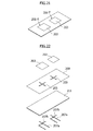
- FIG. 21 is a perspective view which illustrates a transmitting-receiving-separated dual-polarization patch antenna which uses a microstrip line as a feed line
- Figure 22 is an exploded view of the patch antenna.
- the transmitting-receiving-separated dual-polarization patch antenna includes a patch antenna 201-T for a transmitting band and a patch antenna 201-R for a receiving band.
- the patch antenna 201-T for transmitting band is constituted by a patch 203, a cross-shaped feed slot 205, which is located below the patch 203, and feed lines 207a and 207b, which are located below the feed slot 205.
- the patch antenna 201-R has a similar configuration.
- the feed slot 205 of the patch antenna 201-T, 201-R is formed on a common ground conductor plate 209.
- a dielectric substrate 211 is arranged between the ground conductor plate 209 and the feed line 207a, 207b. Note that the transmitting-receiving-separated dual-polarization patch antenna does not include any configuration for implementing the bandstop, which is included in the antenna according to Patent Literature 2.
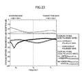
- f R denotes a center frequency of the receiving band
- f T denotes a center frequency of the transmitting band
- f 0 denotes a center frequency between a lower limit frequency of the receiving band and an upper limit frequency of the transmitting band, respectively
- f R 0.953 f 0
- f T 1.047 f 0 .
- the transmitting-receiving-separated dual-polarization patch antenna As is clear from the coupling characteristic, according to the transmitting-receiving-separated dual-polarization patch antenna, coupling between transmission and reception among cross polarized waves (i.e., among vertically polarized waves for the receiving band and horizontally polarized waves for the transmitting band, and among horizontally polarized waves for the receiving band and vertically polarized waves for the transmitting band) can be reduced to -40 dB or lower, however, with respect to the coupling between transmission and reception among the same polarized waves (i.e., among vertically polarized waves for the receiving band and vertically polarized waves for the transmitting band, and among horizontally polarized waves for the receiving band and horizontally polarized waves for the transmitting band), the worst case value becomes -20 dB or higher. As described above, in the transmitting-receiving-separated dual-polarization patch antenna described above, coupling among the same polarized waves becomes intense
- Multi-Input Multi-Output becomes the main technology, and in order to apply the above-described transmitting-receiving-separated patch antennas to MIMO, it becomes necessary to reduce coupling between transmission and reception while implementing sharing of polarized waves at the same time for both the transmitting band and the receiving band.
- MIMO Multi-Input Multi-Output
- the purpose of the present invention is to provide a transmitting-receiving-separated dual-polarization antenna capable of reducing coupling between transmission and reception while implementing sharing of polarized waves for both the transmitting band and the receiving band at the same time.
- a transmitting-receiving-separated dual-polarization antenna includes a patch antenna for a transmitting band and a patch antenna for a receiving band.
- the patch antenna for the transmitting band and the patch antenna for the receiving band have a predetermined spacing therebetween.
- Each of the patch antenna for the transmitting band and the patch antenna for the receiving band comprises an upper-stage ground conductor, a lower-stage ground conductor, a feed line arranged between the ground conductors, a feed slot formed on the upper-stage ground conductor, a patch electromagnetically coupled with the feed line via the feed slot, and an electromagnetic shielding member connected with the upper-stage ground conductor and the lower-stage ground conductor in a state in which the electromagnetic shielding member is located around the feed line, and the feed line includes independent feeding conductors corresponding to respective polarized waves.
- the electromagnetic shielding member is formed by multiple through holes, which are arranged around the feed line at predetermined spacing and extended from the upper-stage ground conductor to the lower-stage ground conductor, for example.
- the electromagnetic shielding member may be formed by a metal plate, which is arranged around the feed line and extended from the upper-stage ground conductor to the lower-stage ground conductor.
- the spacing for arranging the patch antenna for the transmitting band and the patch antenna for the receiving band be set at 0.5 ⁇ 0 ( ⁇ 0 is a wavelength of a center frequency between a lower limit frequency for the receiving band and an upper limit frequency for the transmitting band) or smaller.
- the feed slot may be square-shaped or cross-shaped.
- a transmitting-receiving-separated dual-polarization antenna having an allayed configuration may be implemented by arranging multiple stages of the transmitting-receiving-separated dual-polarization antennas.
- coupling between transmission and reception can be reduced while implementing sharing of polarized waves for both the transmitting band and the receiving band.
- the element spacing among the patch antennas for the transmitting band and the patch antennas for the receiving band is set as narrow as 0.4 ⁇ 0 ( ⁇ 0 is a wavelength of the center frequency between a lower limit frequency for the receiving band and an upper limit frequency for the transmitting band)
- coupling between transmission and reception as low as -30 dB or lower can be implemented.
- it is enabled to downsize a bandpass filter provided at a subsequent stage by omitting a diplexer which may otherwise be arranged inside a transmitting and receiving front end circuit.
- f 0 and ⁇ 0 are a center frequency between a lower limit frequency of the receiving band and an upper limit frequency of the transmitting band and a wavelength thereof, respectively
- f R and X R are a center frequency of the receiving band and a wavelength thereof, respectively
- f T and ⁇ T are a center frequency of the transmitting band and a wavelength thereof, respectively
- FIGS 1 and 2 are a perspective view and a plan view which illustrate an embodiment of a transmitting-receiving-separated dual-polarization patch antenna according to the present invention.
- the direction of z-axis is perpendicular to the ground and the xy plane is a plane parallel to the ground.
- a transmitting-receiving-separated antenna according to the present embodiment includes a patch antenna 3-T for a transmitting band and a patch antenna 3-R for a receiving band, which are installed on a conductor substrate 1.
- the patch antenna 3-R for the receiving band and the patch antenna 3-T for the transmitting band are arranged at spacing d between them of 0.5 ⁇ 0 or smaller, and the spacing d is set at 0.4 ⁇ 0 in the present embodiment.
- the patch antenna 3-T for the transmitting band and the patch antenna 3-R for the receiving band include at least four layers constituted by metal plates as illustrated in the exploded perspective view in Figure 3 .
- the first layer (the top layer) is a patch 5 having a square shape, which is an excitation element (an antenna element).
- the patch 5 is formed in the center of an upper surface of a dielectric substrate 7.
- the second layer is an upper-stage ground conductor 9.
- the upper-stage ground conductor 9 is adhered to an upper surface of a dielectric substrate 11, and a feed slot 13 is formed in the center thereof.
- the third layer is a feed line 15.
- the feed line 15 includes a feeding conductor 15a for horizontally polarized wave and a feeding conductor 15b for vertically polarized wave, which are formed on an upper surface of a dielectric substrate 17, and a bridge conductor 15c, which will be described below.
- the fourth layer (the bottom layer) is a lower-stage ground conductor 19.
- the lower-stage ground conductor 19 is adhered to a lower surface of the dielectric substrate 17, and a slot 21 is formed in the center thereof. Further, the above-described bridge conductor 15c is formed in an inside of the slot 21. Note that the upper-stage ground conductor 9, the dielectric substrate 11, the feed line 15, the dielectric substrate 17, and the lower-stage ground conductor 19 constitute a feed line known as a triplate feed line. Note that in the present embodiment, dielectric substrates of which relative dielectric constant ⁇ r is about 3.3 are used for the dielectric substrates 7, 11, and 17.
- the patch 5, the upper-stage ground conductor 9, the feed line 15, and the lower-stage ground conductor 19 described above are constituted by a metal foil such as a copper foil, respectively, and are patterned by using a method for forming a printed wiring pattern (a method in which a predetermined metal foil pattern is formed on a surface of a dielectric by etching processing and the like).
- a method for forming a printed wiring pattern a method in which a predetermined metal foil pattern is formed on a surface of a dielectric by etching processing and the like.
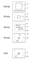
- FIGS 4(a) through 4(d) illustrate a planar structure of the patch 5, the upper-stage ground conductor 9, the planar structure of the feed line 15, and the lower-stage ground conductor 19, respectively.
- the patch 5 is formed so as to form a square about 0.25 ⁇ R on a side
- the feed slot 13, which is provided on the upper-stage ground conductor 9, is formed so as to form a square about 0.1 ⁇ R on a side, for example.
- the structures of the patch 5 and the feed slot 13 are determined according to the resonance frequency band, and each side of the patch 7 is set at 0.228 ⁇ R and each side of the feed slot 13 is set at 0.125 ⁇ R , respectively.
- the feed slot 13 according to the present embodiment is formed so as to be square-shaped, however, the configuration of the feed slot 13 is not limited to this, and similar functions can be achieved if a cross-shaped feed slot 27, which is illustrated in Figure 5 , is used.
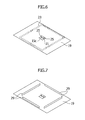
- the upper-stage ground conductor 9 and the lower-stage ground conductor 19 are electrically short-circuited via through holes 23, which penetrate through the dielectric substrates 11 and 17. Accordingly, both ground conductors 9 and 19 have the same potential.
- the through holes 23 are arranged at spacing of 0.01 to 0.02 ⁇ R on each side of the square-shaped area about 0.25 to 0.35 ⁇ R on a side. Note that the center point of the square-shaped area and that of the patch 5 have the same value of xz coordinates (see Figure 2 ).
- Metal plates 29 illustrated in Figure 7 can be used instead of the above-described through holes 23.
- the metal plates 29 have a height substantially the same as that of the through holes 23, and are provided along respective sides of the above-described square-shaped area.
- slits through which the metal plate 29 is allowed to penetrate are formed in the upper-stage ground conductor 9, the dielectric substrate 11, the dielectric substrate 17, and the lower-stage ground conductor 19, respectively, and upper edges and lower edges of the metal plates 29 penetrated through the slits are connected with an upper surface of the upper-stage ground conductor 9 and a lower surface of the lower-stage ground conductor 19, respectively, by using means such as soldering.
- the values of the structure parameter for generating resonance in the receiving band are as described above.
- the values of the structure parameter set in generating resonance in the transmission band are values obtained by substituting the wavelength ⁇ R with the wavelength ⁇ T .
- the patch antenna 3-R for the receiving band and the patch antenna 3-T for the transmitting band illustrated in Figure 1 and the patch antenna 3-T for the transmitting band operate only for the frequency band used by the respective antennas by setting the structure parameter values in the above-described manner.
- each end of the conductor element 15b which faces the notch part is connected with the above-described bridge conductor 15c via through holes 25 which penetrate through the dielectric substrate 17.
- the bridge conductor 15c and the through holes 25 are bridge-connected while bypassing the contact between the conductor element 15b and the conductor element 15a, which are divided by the notch into two portions.
- the bridge conductor 15c may be provided inside the feed slot 13 of the upper-stage ground conductor 9.
- the antenna according to the present invention be manufactured by using a multilayer substrate as described above in consideration of its configuration.
- the patch antenna 3-R for the receiving band one end of the feeding conductor 15a and one end of the feeding conductor 15b are the feeding points for horizontally polarized waves and vertically polarized waves, respectively.
- This also applies to the patch antenna 3-T for the transmitting band.
- the patch antenna 3-T for the transmitting band and the patch antenna 3-R for the receiving band perform a transmitting operation and a receiving operation, respectively, by sharing polarized waves due to electromagnetic coupling between the patch 5 and the feed line 15 via the corresponding feed slot 13.
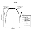
- Figure 8 illustrates results of simulation of return loss occurring in the antenna according to the present embodiment.
- the fractional bandwidth in which the return loss is -9.6 dB or lower, is about 1.1% with respect to horizontally polarized waves in the receiving band of which the fractional bandwidth is the narrowest.
- Figure 9 illustrates characteristics of coupling between transmission and reception of the antenna according to the present embodiment.
- the coupling value becomes high in the case where the waves are polarized in the same direction in both the transmitting band and the receiving band, however, as is clear from the fact that the worst case value is -30 dB, which is a value in the receiving band in which the waves are horizontally polarized waves, the antenna according to the present embodiment has excellent characteristics as a whole.
- the coupling between transmission and reception among cross polarized waves has excellent values of -60 dB or lower for both the transmitting band and the receiving band.
- the coupling between transmission and reception can be reduced to -30 dB or lower while implementing sharing of polarized waves in both the transmitting band and the receiving band.
- the through holes 23 illustrated in Figure 6 or the metal plates 29 illustrated in Figure 7 have a function as an electromagnetic shielding member which suppresses coupling between transmission and reception.
- Figure 10 illustrates a radiation pattern of vertically polarized waves in the receiving band on the xy plane of the antenna according to the present embodiment
- Figure 11 illustrates a radiation pattern of horizontally polarized waves in the receiving band on the xy plane of the antenna
- Figure 12 illustrates a radiation pattern of the vertically polarized waves in the transmitting band on the xy plane of the antenna
- Figure 13 illustrates a radiation pattern of horizontally polarized waves in the transmitting band on the xy plane of the antenna, respectively.
- an excellent radiation pattern with a half bandwidth of about 80° can be achieved both in the transmitting band and the receiving band and regardless of the type of polarization.
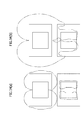
- Figure 14(a) illustrates the distribution of field intensity with respect to the antenna according to the present embodiment, which is observed when horizontally polarized waves in the receiving band are excited.
- Figure 14(b) illustrates the distribution of field intensity with respect to the antenna of Comparative Example, in which no through holes 23 are provided.
- the antenna of the present embodiment having the through holes 23 the amount of electric field creeping from the excited patch 5 to a non-excited patch 5 can be effectively reduced due to the electromagnetic shield action of the through holes 23.
- the amount of coupling between the patch antenna 3-R for the receiving band and the patch antenna 3-T for the transmitting band is reduced.
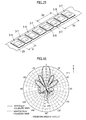
- Figure 15 illustrates a transmitting-receiving-separated dual-polarization antenna having an allayed configuration, in which multiple stages of the transmitting-receiving-separated dual-polarization patch antenna illustrated in Figure 1 are arranged on the metal plate 29.
- the patch antenna 3-T for the transmitting band and the patch antenna 3-R for the receiving band are alternately arranged.
- the spacing between mutually adjacent patch antennas 3-T for the transmitting band and the spacing between mutually adjacent patch antennas 3-R for the receiving band are set at a value 2d, which is twice as large as the element spacing (the spacing between the patches 5) d illustrated in Figure 2 .
- Figures 16 and 17 illustrate the radiation pattern on the yz plane of the transmitting-receiving-separated dual-polarization patch antenna having an allayed configuration, in which multiple stages of the transmitting-receiving-separated dual-polarization patch antenna illustrated in Figure 1 with the element spacing d of 0.4 ⁇ 0 are arranged, in the receiving band and the transmitting band, respectively.
- Figures 18 and 19 illustrate the radiation pattern on the yz plane of Comparison Example in the receiving band and the transmitting band, respectively, in a case in which the element spacing d is 0.5 ⁇ 0 . Note that the radiation patterns are observed when the respective feeding points are excited at the same phase and by the same amplitude.
- a solid line and a broken line denote the radiation pattern for vertically polarized waves and that for horizontally polarized waves, respectively.
- the element spacing d is set at 0.5 ⁇ 0 or narrower so that the coupling amount can be reduced while suppressing the grating lobe at the same time.
Landscapes
- Physics & Mathematics (AREA)
- Electromagnetism (AREA)
- Variable-Direction Aerials And Aerial Arrays (AREA)
- Waveguide Aerials (AREA)
- Details Of Aerials (AREA)
Abstract
Description
- The present invention relates to a transmitting-receiving-separated dual-polarization antenna particularly preferable for use at a mobile communication base station.
- In order to secure power per bit, which has been increasing as the data transmission speed becomes higher, it is useful to reduce the loss in a feed system (see Non-Patent
Literature 1, for example).Figure 20 illustrates a configuration in which a transmitting and receiving front end circuit and an antenna are integrally implemented, which is one of the means for implementing the reduction of loss in a feed system. - In
Figure 20 , adiplexer 103, which separates transmitting and receiving bands, is provided immediately below anantenna 101, andbandpass filters diplexer 103. A low noise amplifier (LNA) 109, which is arranged in a stage subsequent to thebandpass filter 105, and a power amplifier (PA) 111, which is arranged in a stage subsequent to thebandpass filter 107, are provided in order to increase the level of signals in the receiving band and the transmitting band, respectively. - According to the above-described configuration, the reduction of a noise figure (NF) can be implemented for the receiving band, and the reduction of required radiation power can be implemented for the transmitting band. However, if the above-described configuration is applied to a frequency division duplex (FDD) system, a required value becomes high for the bandstop amount for signals in unnecessary frequency bands in order to separate signals in the transmitting band, and accordingly, a problem may arise such that it becomes necessary to respond to the high required value by using a multi-stage large diplexers and bandpass filters.
- Under these circumstances, in order to implement a small-sized filter, the transmitting-receiving-separated antennas according to
Patent Literatures 1 to 3 have been proposed, which additionally include function of a diplexer. The transmitting-receiving-separated antennas implement reduction of the number of stages of filters arranged at stages subsequent to the antenna by suppressing cross coupling between an antenna for the transmitting band and an antenna for the receiving band (this phenomenon will be hereafter referred to as "coupling between transmission and reception "). The antenna according toPatent Literature 1 reduces coupling between transmission and reception in a configuration in which polarized waves in the transmitting and those in the receiving band are crossed one another, and coupling between transmission and reception as low as about -35 dB can be achieved thereby. The antenna according toPatent Literature 2 reduces coupling between transmission and reception in the transmitting band, even among the same polarized waves, to a level as low as about -30 dB by providing a parasitic element intended as a bandstop. The antenna according toPatent Literature 3 reduces coupling between transmission and reception to a level as low as about -50 dB by using circular polarization antennas of the same nutation direction as antennas for the transmitting band and the receiving band and by allowing one element structure to rotate. - The above-described antennas according to
Patent Literatures Figure 21 is a perspective view which illustrates a transmitting-receiving-separated dual-polarization patch antenna which uses a microstrip line as a feed line, andFigure 22 is an exploded view of the patch antenna. The transmitting-receiving-separated dual-polarization patch antenna includes a patch antenna 201-T for a transmitting band and a patch antenna 201-R for a receiving band. The patch antenna 201-T for transmitting band is constituted by apatch 203, across-shaped feed slot 205, which is located below thepatch 203, andfeed lines feed slot 205. The patch antenna 201-R has a similar configuration. Thefeed slot 205 of the patch antenna 201-T, 201-R is formed on a commonground conductor plate 209. In addition, adielectric substrate 211 is arranged between theground conductor plate 209 and thefeed line Patent Literature 2. - In the transmitting-receiving-separated dual-polarization patch antenna, power is fed to the
patch 203 of the patch antenna 201-T for the transmitting band so that polarized waves are shared by electromagnetic coupling with thefeed line corresponding feed slot 205. Thepatch 203 of the patch antenna 201-R for the receiving band has a similar configuration.Figure 23 illustrates a characteristic of coupling between transmission and reception with respect to the transmitting-receiving-separated dual-polarization patch antenna. In this drawing, fR denotes a center frequency of the receiving band, fT denotes a center frequency of the transmitting band, and f0 denotes a center frequency between a lower limit frequency of the receiving band and an upper limit frequency of the transmitting band, respectively, and fR = 0.953 f0, fT = 1.047 f0. - As is clear from the coupling characteristic, according to the transmitting-receiving-separated dual-polarization patch antenna, coupling between transmission and reception among cross polarized waves (i.e., among vertically polarized waves for the receiving band and horizontally polarized waves for the transmitting band, and among horizontally polarized waves for the receiving band and vertically polarized waves for the transmitting band) can be reduced to -40 dB or lower, however, with respect to the coupling between transmission and reception among the same polarized waves (i.e., among vertically polarized waves for the receiving band and vertically polarized waves for the transmitting band, and among horizontally polarized waves for the receiving band and horizontally polarized waves for the transmitting band), the worst case value becomes -20 dB or higher. As described above, in the transmitting-receiving-separated dual-polarization patch antenna described above, coupling among the same polarized waves becomes intense.
-
- [Patent Literature 1] Japanese Patent Application Laid-Open No.
05-41608 - [Patent Literature 2] Japanese Patent Application Laid-Open No.
2009-71795 - [Patent Literature 3] Japanese Patent Application Laid-Open No.
05-175727 - [Non-Patent Literature 1] Keizo CHO, Ryo YAMAGUCHI, and Huiling JIANG, "Base Station and Terminal Antenna Technologies Required for Next Generation Mobile Communication Systems", Journal of the Institute of Electronics, Information and Communication Engineers, Vol. J85-B, No. 9, pp. 886-900 (Sept. 2008)
- In future mobile communications typified by Long Term Evolution (LTE), Multi-Input Multi-Output (MIMO) becomes the main technology, and in order to apply the above-described transmitting-receiving-separated patch antennas to MIMO, it becomes necessary to reduce coupling between transmission and reception while implementing sharing of polarized waves at the same time for both the transmitting band and the receiving band. However, as described above, if polarized waves are shared in the conventional transmitting-receiving-separated patch antenna, a problem may arise such that coupling between transmission and reception among same polarized waves may not be reduced.
- In order to solve the above-described problems, the purpose of the present invention is to provide a transmitting-receiving-separated dual-polarization antenna capable of reducing coupling between transmission and reception while implementing sharing of polarized waves for both the transmitting band and the receiving band at the same time.
- According to an aspect of the present invention, a transmitting-receiving-separated dual-polarization antenna includes a patch antenna for a transmitting band and a patch antenna for a receiving band. The patch antenna for the transmitting band and the patch antenna for the receiving band have a predetermined spacing therebetween. Each of the patch antenna for the transmitting band and the patch antenna for the receiving band comprises an upper-stage ground conductor, a lower-stage ground conductor, a feed line arranged between the ground conductors, a feed slot formed on the upper-stage ground conductor, a patch electromagnetically coupled with the feed line via the feed slot, and an electromagnetic shielding member connected with the upper-stage ground conductor and the lower-stage ground conductor in a state in which the electromagnetic shielding member is located around the feed line, and the feed line includes independent feeding conductors corresponding to respective polarized waves.
- The electromagnetic shielding member is formed by multiple through holes, which are arranged around the feed line at predetermined spacing and extended from the upper-stage ground conductor to the lower-stage ground conductor, for example. In addition, the electromagnetic shielding member may be formed by a metal plate, which is arranged around the feed line and extended from the upper-stage ground conductor to the lower-stage ground conductor.
- It is preferable if the spacing for arranging the patch antenna for the transmitting band and the patch antenna for the receiving band be set at 0.5 λ0 (λ0 is a wavelength of a center frequency between a lower limit frequency for the receiving band and an upper limit frequency for the transmitting band) or smaller. In addition, the feed slot may be square-shaped or cross-shaped. Further, a transmitting-receiving-separated dual-polarization antenna having an allayed configuration may be implemented by arranging multiple stages of the transmitting-receiving-separated dual-polarization antennas.
- According to the present invention, coupling between transmission and reception can be reduced while implementing sharing of polarized waves for both the transmitting band and the receiving band. For example, even in a case in which the element spacing among the patch antennas for the transmitting band and the patch antennas for the receiving band is set as narrow as 0.4 λ0 (λ0 is a wavelength of the center frequency between a lower limit frequency for the receiving band and an upper limit frequency for the transmitting band), coupling between transmission and reception as low as -30 dB or lower can be implemented. In addition, according to the present invention, it is enabled to downsize a bandpass filter provided at a subsequent stage by omitting a diplexer which may otherwise be arranged inside a transmitting and receiving front end circuit.
-
- [
Figure 1] Figure 1 is a perspective view which illustrates an embodiment of a transmitting-receiving-separated dual-polarization patch antenna according to the present invention. - [
Figure 2] Figure 2 is a plan view which illustrates an antenna according to an embodiment. - [
Figure 3] Figure 3 is an exploded perspective view which illustrates a patch antenna for a transmitting band and a patch antenna for a receiving band. - [
Figure 4] Figures 4(a) through 4(d) are plan views which illustrate a planar structure of a patch, an upper-stage ground conductor, a feed line, and a lower-stage ground conductor, respectively. - [
Figure 5] Figure 5 is a plan view which illustrates another example of a feed slot. - [
Figure 6] Figure 6 is a perspective view which illustrates a mode of arrangement of through holes. - [
Figure 7] Figure 7 is a perspective view which illustrates metal plates used instead of the through holes. - [
Figure 8] Figure 8 is a graph which illustrates return loss characteristics of the antenna according to an embodiment. - [
Figure 9] Figure 9 is a graph which illustrates transmission-reception coupling characteristics of the antenna according to an embodiment. - [
Figure 10] Figure 10 is a graph which illustrates a radiation pattern of vertically polarized waves in the receiving band on the xy plane of the antenna according to an embodiment. - [
Figure 11] Figure 11 is a graph which illustrates a radiation pattern of horizontally polarized waves in the receiving band on the xy plane of the antenna according to an embodiment. - [
Figure 12] Figure 12 is a graph which illustrates a radiation pattern of the vertically polarized waves in the transmitting band on the xy plane of the antenna according to an embodiment. - [
Figure 13] Figure 13 is a graph which illustrates a radiation pattern of horizontally polarized waves in the transmitting band on the xy plane of the antenna according to an embodiment. - [
Figure 14] Figure 14(a) is a view which illustrates the distribution of field intensity of the antenna according to an embodiment. -
Figure 14(b) is a view which illustrates the distribution of field intensity observed when no through holes are provided. - [
Figure 15] Figure 15 is a perspective view which illustrates a transmitting-receiving-separated dual-polarization patch antenna having an allayed configuration. - [
Figure 16] Figure 16 is a graph which illustrates a radiation pattern of waves in the receiving band on the yz plane of the transmitting-receiving-separated dual-polarization patch antenna having an allayed configuration. - [
Figure 17] Figure 17 is a graph which illustrates a radiation pattern of waves in the transmitting band on the yz plane of the transmitting-receiving-separated dual-polarization patch antenna having an allayed configuration. - [
Figure 18] Figure 18 is a graph which illustrates a radiation pattern of waves in the receiving band on the yz plane of the transmitting-receiving-separated dual-polarization patch antenna having an allayed configuration with altered element spacing. - [
Figure 19] Figure 19 is a graph which illustrates a radiation pattern of waves in the transmitting band on the yz plane of the transmitting-receiving-separated dual-polarization patch antenna having an allayed configuration with altered element spacing. - [
Figure 20] Figure 20 is a block diagram which illustrates a configuration in which the transmitting and receiving front end circuit and the antenna are integrated together. - [
Figure 21] Figure 21 is a perspective view which illustrates the conventional transmitting-receiving-separated dual-polarization patch antenna. - [
Figure 22] Figure 22 is a an exploded view which illustrates the conventional transmitting-receiving-separated dual-polarization patch antenna. - [
Figure 23] Figure 23 is a graph which illustrates a characteristic of the conventional transmitting-receiving-separated dual-polarization patch antenna of coupling between transmission and reception. - In the following description, f0 and λ0 are a center frequency between a lower limit frequency of the receiving band and an upper limit frequency of the transmitting band and a wavelength thereof, respectively, fR and XR are a center frequency of the receiving band and a wavelength thereof, respectively, fT and λT are a center frequency of the transmitting band and a wavelength thereof, respectively, and fR = 0.953 f0 (wavelength λR = 1.049 λ0), fT = 1.047 f0 (wavelength λT = 0.955 λ0).
-
Figures 1 and 2 are a perspective view and a plan view which illustrate an embodiment of a transmitting-receiving-separated dual-polarization patch antenna according to the present invention. In these drawings, the direction of z-axis is perpendicular to the ground and the xy plane is a plane parallel to the ground. A transmitting-receiving-separated antenna according to the present embodiment includes a patch antenna 3-T for a transmitting band and a patch antenna 3-R for a receiving band, which are installed on aconductor substrate 1. The patch antenna 3-R for the receiving band and the patch antenna 3-T for the transmitting band are arranged at spacing d between them of 0.5 λ0 or smaller, and the spacing d is set at 0.4 λ0 in the present embodiment. - The patch antenna 3-T for the transmitting band and the patch antenna 3-R for the receiving band include at least four layers constituted by metal plates as illustrated in the exploded perspective view in
Figure 3 . The first layer (the top layer) is apatch 5 having a square shape, which is an excitation element (an antenna element). Thepatch 5 is formed in the center of an upper surface of adielectric substrate 7. The second layer is an upper-stage ground conductor 9. The upper-stage ground conductor 9 is adhered to an upper surface of adielectric substrate 11, and afeed slot 13 is formed in the center thereof. The third layer is afeed line 15. Thefeed line 15 includes afeeding conductor 15a for horizontally polarized wave and afeeding conductor 15b for vertically polarized wave, which are formed on an upper surface of adielectric substrate 17, and abridge conductor 15c, which will be described below. The fourth layer (the bottom layer) is a lower-stage ground conductor 19. - The lower-
stage ground conductor 19 is adhered to a lower surface of thedielectric substrate 17, and aslot 21 is formed in the center thereof. Further, the above-describedbridge conductor 15c is formed in an inside of theslot 21. Note that the upper-stage ground conductor 9, thedielectric substrate 11, thefeed line 15, thedielectric substrate 17, and the lower-stage ground conductor 19 constitute a feed line known as a triplate feed line. Note that in the present embodiment, dielectric substrates of which relative dielectric constant εr is about 3.3 are used for thedielectric substrates - The
patch 5, the upper-stage ground conductor 9, thefeed line 15, and the lower-stage ground conductor 19 described above are constituted by a metal foil such as a copper foil, respectively, and are patterned by using a method for forming a printed wiring pattern (a method in which a predetermined metal foil pattern is formed on a surface of a dielectric by etching processing and the like). When thedielectric substrates patch 5, the upper-stage ground conductor 9, thefeed line 15, and the lower-stage ground conductor 19 are located on a common axis. -
Figures 4(a) through 4(d) illustrate a planar structure of thepatch 5, the upper-stage ground conductor 9, the planar structure of thefeed line 15, and the lower-stage ground conductor 19, respectively. Now, values of structure parameter for generating resonance in the receiving band will be described. Thepatch 5 is formed so as to form a square about 0.25 λR on a side, and thefeed slot 13, which is provided on the upper-stage ground conductor 9, is formed so as to form a square about 0.1 λR on a side, for example. The structures of thepatch 5 and thefeed slot 13 are determined according to the resonance frequency band, and each side of thepatch 7 is set at 0.228 λR and each side of thefeed slot 13 is set at 0.125 λR, respectively. Thefeed slot 13 according to the present embodiment is formed so as to be square-shaped, however, the configuration of thefeed slot 13 is not limited to this, and similar functions can be achieved if across-shaped feed slot 27, which is illustrated inFigure 5 , is used. - As illustrated in
Figure 3 , the upper-stage ground conductor 9 and the lower-stage ground conductor 19 are electrically short-circuited via throughholes 23, which penetrate through thedielectric substrates ground conductors Figures 4 through 6 , the throughholes 23 are arranged at spacing of 0.01 to 0.02 λR on each side of the square-shaped area about 0.25 to 0.35 λR on a side. Note that the center point of the square-shaped area and that of thepatch 5 have the same value of xz coordinates (seeFigure 2 ). -
Metal plates 29 illustrated inFigure 7 can be used instead of the above-described throughholes 23. Themetal plates 29 have a height substantially the same as that of the throughholes 23, and are provided along respective sides of the above-described square-shaped area. In short-circuiting the upper-stage ground conductor 9 and the lower-stage ground conductor 19 by using themetal plates 29, slits through which themetal plate 29 is allowed to penetrate are formed in the upper-stage ground conductor 9, thedielectric substrate 11, thedielectric substrate 17, and the lower-stage ground conductor 19, respectively, and upper edges and lower edges of themetal plates 29 penetrated through the slits are connected with an upper surface of the upper-stage ground conductor 9 and a lower surface of the lower-stage ground conductor 19, respectively, by using means such as soldering. The values of the structure parameter for generating resonance in the receiving band are as described above. The values of the structure parameter set in generating resonance in the transmission band are values obtained by substituting the wavelength λR with the wavelength λT. The patch antenna 3-R for the receiving band and the patch antenna 3-T for the transmitting band illustrated inFigure 1 and the patch antenna 3-T for the transmitting band operate only for the frequency band used by the respective antennas by setting the structure parameter values in the above-described manner. - Incidentally, in order to share polarized waves, it is necessary to separate between the feeding
conductor 15a for horizontally polarized wave and thefeeding conductor 15b for vertically polarized wave. This is the reason why the center of theconductor element 15b is cut out. Each end of theconductor element 15b which faces the notch part is connected with the above-describedbridge conductor 15c via throughholes 25 which penetrate through thedielectric substrate 17. As described above, thebridge conductor 15c and the throughholes 25 are bridge-connected while bypassing the contact between theconductor element 15b and theconductor element 15a, which are divided by the notch into two portions. Note that thebridge conductor 15c may be provided inside thefeed slot 13 of the upper-stage ground conductor 9. - It is preferable that the antenna according to the present invention be manufactured by using a multilayer substrate as described above in consideration of its configuration. In the patch antenna 3-R for the receiving band, one end of the
feeding conductor 15a and one end of thefeeding conductor 15b are the feeding points for horizontally polarized waves and vertically polarized waves, respectively. This also applies to the patch antenna 3-T for the transmitting band. Further, the patch antenna 3-T for the transmitting band and the patch antenna 3-R for the receiving band perform a transmitting operation and a receiving operation, respectively, by sharing polarized waves due to electromagnetic coupling between thepatch 5 and thefeed line 15 via thecorresponding feed slot 13. -
Figure 8 illustrates results of simulation of return loss occurring in the antenna according to the present embodiment. As is clear from the return loss characteristic, according to the antenna of the present embodiment, the fractional bandwidth, in which the return loss is -9.6 dB or lower, is about 1.1% with respect to horizontally polarized waves in the receiving band of which the fractional bandwidth is the narrowest. -
Figure 9 illustrates characteristics of coupling between transmission and reception of the antenna according to the present embodiment. As is clear from the characteristics of coupling between transmission and reception, the coupling value becomes high in the case where the waves are polarized in the same direction in both the transmitting band and the receiving band, however, as is clear from the fact that the worst case value is -30 dB, which is a value in the receiving band in which the waves are horizontally polarized waves, the antenna according to the present embodiment has excellent characteristics as a whole. The coupling between transmission and reception among cross polarized waves has excellent values of -60 dB or lower for both the transmitting band and the receiving band. As described above, according to the antenna of the present embodiment, the coupling between transmission and reception can be reduced to -30 dB or lower while implementing sharing of polarized waves in both the transmitting band and the receiving band. This is because the throughholes 23 illustrated inFigure 6 or themetal plates 29 illustrated inFigure 7 have a function as an electromagnetic shielding member which suppresses coupling between transmission and reception. -
Figure 10 illustrates a radiation pattern of vertically polarized waves in the receiving band on the xy plane of the antenna according to the present embodiment,Figure 11 illustrates a radiation pattern of horizontally polarized waves in the receiving band on the xy plane of the antenna,Figure 12 illustrates a radiation pattern of the vertically polarized waves in the transmitting band on the xy plane of the antenna, andFigure 13 illustrates a radiation pattern of horizontally polarized waves in the transmitting band on the xy plane of the antenna, respectively. As is clear from these drawings, according to the antenna of the present embodiment, an excellent radiation pattern with a half bandwidth of about 80° can be achieved both in the transmitting band and the receiving band and regardless of the type of polarization. -
Figure 14(a) illustrates the distribution of field intensity with respect to the antenna according to the present embodiment, which is observed when horizontally polarized waves in the receiving band are excited.Figure 14(b) illustrates the distribution of field intensity with respect to the antenna of Comparative Example, in which no throughholes 23 are provided. According to the antenna of the present embodiment having the throughholes 23, the amount of electric field creeping from theexcited patch 5 to anon-excited patch 5 can be effectively reduced due to the electromagnetic shield action of the through holes 23. To paraphrase this, the amount of coupling between the patch antenna 3-R for the receiving band and the patch antenna 3-T for the transmitting band is reduced. -
Figure 15 illustrates a transmitting-receiving-separated dual-polarization antenna having an allayed configuration, in which multiple stages of the transmitting-receiving-separated dual-polarization patch antenna illustrated inFigure 1 are arranged on themetal plate 29. In the antenna, the patch antenna 3-T for the transmitting band and the patch antenna 3-R for the receiving band are alternately arranged. Further, the spacing between mutually adjacent patch antennas 3-T for the transmitting band and the spacing between mutually adjacent patch antennas 3-R for the receiving band are set at avalue 2d, which is twice as large as the element spacing (the spacing between the patches 5) d illustrated inFigure 2 . -
Figures 16 and17 illustrate the radiation pattern on the yz plane of the transmitting-receiving-separated dual-polarization patch antenna having an allayed configuration, in which multiple stages of the transmitting-receiving-separated dual-polarization patch antenna illustrated inFigure 1 with the element spacing d of 0.4 λ0 are arranged, in the receiving band and the transmitting band, respectively.Figures 18 and19 illustrate the radiation pattern on the yz plane of Comparison Example in the receiving band and the transmitting band, respectively, in a case in which the element spacing d is 0.5 λ0. Note that the radiation patterns are observed when the respective feeding points are excited at the same phase and by the same amplitude. InFigures 16 through 19 , a solid line and a broken line denote the radiation pattern for vertically polarized waves and that for horizontally polarized waves, respectively. As is clear from comparisons betweenFigures 16 and17 andFigures 18 and19 , if the element spacing d is 0.4 λ0, then the maximum sidelobe level within the test range becomes about 13 dB, and thereby the grating lobe is more suppressed compared with the case where d = 0.5 λ0. In the transmitting-receiving-separated dual-polarization patch antenna having an allayed configuration according to the present invention, the element spacing d is set at 0.5 λ0 or narrower so that the coupling amount can be reduced while suppressing the grating lobe at the same time. -
- 1
- Metal conductor
- 3-T
- Patch antenna for transmitting band
- 3-R
- Patch antenna for receiving band
- 5
- Patch
- 7
- Dielectric substrate
- 9
- Upper-stage ground conductor
- 11
- Dielectric substrate
- 13
- Feed slot
- 15
- Feed line
- 15a
- Feeding conductor for horizontally polarized wave
- 15b
- Feeding conductor for vertically polarized wave
- 15c
- Bridge conductor
- 17
- Dielectric substrate
- 19
- Lower-stage ground conductor
- 21
- Slot
- 23,25
- Through hole
- 27
- Feed slot
- 29
- Metal plate
Claims (6)
- A transmitting-receiving-separated dual-polarization antenna, comprising:a patch antenna for a transmitting band; anda patch antenna for a receiving band,the patch antenna for the transmitting band and the patch antenna for the receiving band having a predetermined spacing therebetween,wherein each of the patch antenna for the transmitting band and the patch antenna for the receiving band comprises:an upper-stage ground conductor;a lower-stage ground conductor;a feed line arranged between the ground conductors;a feed slot formed on the upper-stage ground conductor;a patch electromagnetically coupled with the feed line via the feed slot; andan electromagnetic shielding member connected with the upper-stage ground conductor and the lower-stage ground conductor in a state in which the electromagnetic shielding member is located around the feed line, andwherein the feed line comprises independent feeding conductors corresponding to respective polarized waves.
- The transmitting-receiving-separated dual-polarization antenna according to Claim 1, wherein the electromagnetic shielding member is formed by multiple through holes, which are arranged around the feed line at predetermined spacing and extended from the upper-stage ground conductor to the lower-stage ground conductor.
- The transmitting-receiving-separated dual-polarization antenna according to Claim 1, wherein the electromagnetic shielding member is formed by a metal plate, which is arranged around the feed line and extended from the upper-stage ground conductor to the lower-stage ground conductor.
- The transmitting-receiving-separated dual-polarization antenna according to Claim 1, wherein the spacing for arranging the patch antenna for the transmitting band and the patch antenna for the receiving band is set at 0.5 λ0 (λ0 is a wavelength of a center frequency between a lower limit frequency for the receiving band and an upper limit frequency for the transmitting band) or smaller.
- The transmitting-receiving-separated dual-polarization antenna according to Claim 1, wherein the feed slot is square-shaped or cross-shaped.
- A transmitting-receiving-separated dual-polarization antenna having an allayed configuration in which multiple stages of the transmitting-receiving-separated dual-polarization antenna according to Claim 1 are arranged.
Applications Claiming Priority (2)
| Application Number | Priority Date | Filing Date | Title |
|---|---|---|---|
| JP2011268961A JP5427226B2 (en) | 2011-12-08 | 2011-12-08 | Transmit / receive split polarization antenna |
| PCT/JP2012/076199 WO2013084585A1 (en) | 2011-12-08 | 2012-10-10 | Transmission/reception-separated polarization-shared antenna |
Publications (3)
| Publication Number | Publication Date |
|---|---|
| EP2790270A1 true EP2790270A1 (en) | 2014-10-15 |
| EP2790270A4 EP2790270A4 (en) | 2015-07-29 |
| EP2790270B1 EP2790270B1 (en) | 2022-05-11 |
Family
ID=48573968
Family Applications (1)
| Application Number | Title | Priority Date | Filing Date |
|---|---|---|---|
| EP12855682.6A Not-in-force EP2790270B1 (en) | 2011-12-08 | 2012-10-10 | Transmission/reception-separated polarization-shared antenna |
Country Status (6)
| Country | Link |
|---|---|
| US (1) | US9379434B2 (en) |
| EP (1) | EP2790270B1 (en) |
| JP (1) | JP5427226B2 (en) |
| KR (1) | KR101602083B1 (en) |
| CN (1) | CN104054215B (en) |
| WO (1) | WO2013084585A1 (en) |
Cited By (1)
| Publication number | Priority date | Publication date | Assignee | Title |
|---|---|---|---|---|
| GB2528839A (en) * | 2014-07-25 | 2016-02-10 | Kathrein Werke Kg | Multiband antenna |
Families Citing this family (21)
| Publication number | Priority date | Publication date | Assignee | Title |
|---|---|---|---|---|
| KR101413986B1 (en) * | 2012-12-26 | 2014-07-04 | 전자부품연구원 | Patch Antenna having a Patch Fed with Mulitiple Signal |
| JP6388199B2 (en) * | 2014-07-03 | 2018-09-12 | 日立金属株式会社 | Antenna device |
| JP6517629B2 (en) * | 2015-08-20 | 2019-05-22 | 株式会社東芝 | Flat antenna device |
| KR102472949B1 (en) * | 2016-03-03 | 2022-12-02 | 삼성전자 주식회사 | Method and electronic device excuting screen security function of electronic device |
| WO2018034868A1 (en) * | 2016-08-18 | 2018-02-22 | Anokiwave, Inc. | Hybrid laminated phased array |
| CN109643846B (en) * | 2016-08-24 | 2021-02-23 | 株式会社村田制作所 | Antenna module |
| CN106329106B (en) * | 2016-10-13 | 2019-10-18 | 哈尔滨工程大学 | A Broadband High Isolation Low Cross-polarized Dual-polarized Microstrip Antenna Array Based on SIW Technology |
| US10505255B2 (en) * | 2017-01-30 | 2019-12-10 | Infineon Technologies Ag | Radio frequency device packages and methods of formation thereof |
| CN106953173B (en) * | 2017-02-23 | 2020-04-28 | 上海华为技术有限公司 | Dual-polarized antenna isolation device and method |
| CN106953157B (en) * | 2017-04-17 | 2023-06-27 | 上海瀚界科技发展有限公司 | An antenna device for a radar sensor |
| GB2569164A (en) * | 2017-12-08 | 2019-06-12 | Cambridge Consultants | Antenna |
| JP6741174B2 (en) * | 2017-12-12 | 2020-08-19 | 株式会社村田製作所 | High frequency module and communication device |
| CN111615777B (en) * | 2018-01-26 | 2023-02-17 | 索尼公司 | antenna equipment |
| CN109728425B (en) * | 2018-12-18 | 2020-06-19 | 南通大学 | Dual-polarized filter patch antenna |
| CN109950691A (en) * | 2018-12-28 | 2019-06-28 | 瑞声科技(新加坡)有限公司 | Millimeter wave array antenna and mobile terminal |
| KR102468914B1 (en) * | 2019-01-30 | 2022-11-18 | 후아웨이 테크놀러지 컴퍼니 리미티드 | dual polarized antenna array |
| CN110048224B (en) | 2019-03-28 | 2021-05-11 | Oppo广东移动通信有限公司 | Antenna module and electronic equipment |
| KR102533885B1 (en) * | 2019-05-31 | 2023-05-18 | 가부시키가이샤 무라타 세이사쿠쇼 | Sub-array antenna, array antenna, antenna module and communication device |
| EP4435973A1 (en) * | 2023-03-23 | 2024-09-25 | u-blox AG | Patch antenna array and method for manufacturing a patch antenna array |
| CN117317596A (en) * | 2023-09-27 | 2023-12-29 | 普罗斯通信技术(苏州)有限公司 | An antenna component and antenna |
| CN120581861A (en) * | 2024-03-01 | 2025-09-02 | 英业达科技有限公司 | Antenna device |
Family Cites Families (17)
| Publication number | Priority date | Publication date | Assignee | Title |
|---|---|---|---|---|
| US4929959A (en) * | 1988-03-08 | 1990-05-29 | Communications Satellite Corporation | Dual-polarized printed circuit antenna having its elements capacitively coupled to feedlines |
| JP3181326B2 (en) | 1991-05-30 | 2001-07-03 | 株式会社東芝 | Microstrip and array antennas |
| JPH082007B2 (en) | 1991-12-24 | 1996-01-10 | 株式会社エイ・ティ・アール光電波通信研究所 | Dual antenna for dual frequency |
| US5241321A (en) * | 1992-05-15 | 1993-08-31 | Space Systems/Loral, Inc. | Dual frequency circularly polarized microwave antenna |
| US5455594A (en) * | 1992-07-16 | 1995-10-03 | Conductus, Inc. | Internal thermal isolation layer for array antenna |
| KR960027054A (en) | 1994-12-16 | 1996-07-22 | 구자홍 | Planar antenna structure for satellite broadcasting reception |
| CA2164669C (en) | 1994-12-28 | 2000-01-18 | Martin Victor Schneider | Multi-branch miniature patch antenna having polarization and share diversity |
| SE9603565D0 (en) * | 1996-05-13 | 1996-09-30 | Allgon Ab | Flat antenna |
| JP2000278039A (en) * | 1999-03-19 | 2000-10-06 | Hitachi Cable Ltd | Dual-polarized antenna |
| US6407704B1 (en) * | 1999-10-22 | 2002-06-18 | Lucent Technologies Inc. | Patch antenna using non-conductive thermo form frame |
| KR20020017775A (en) | 2000-08-31 | 2002-03-07 | 남상임 | A planar antenna using a slot |
| JP3784807B2 (en) * | 2004-02-24 | 2006-06-14 | 株式会社エヌ・ティ・ティ・ドコモ | Microstrip antenna |
| DE102005010895B4 (en) * | 2005-03-09 | 2007-02-08 | Fraunhofer-Gesellschaft zur Förderung der angewandten Forschung e.V. | Aperture-coupled antenna |
| JP4548287B2 (en) * | 2005-09-22 | 2010-09-22 | 三菱電機株式会社 | Antenna device |
| JP2007166115A (en) * | 2005-12-12 | 2007-06-28 | Matsushita Electric Ind Co Ltd | Antenna device |
| JP4881283B2 (en) | 2007-08-20 | 2012-02-22 | 株式会社エヌ・ティ・ティ・ドコモ | Microstrip antenna |
| AU2008310923B9 (en) * | 2007-10-08 | 2014-06-12 | Sensormatic Electronics Llc | RFID patch antenna with coplanar reference ground and floating grounds |
-
2011
- 2011-12-08 JP JP2011268961A patent/JP5427226B2/en active Active
-
2012
- 2012-10-10 US US14/363,498 patent/US9379434B2/en active Active
- 2012-10-10 KR KR1020147015044A patent/KR101602083B1/en not_active Expired - Fee Related
- 2012-10-10 CN CN201280060356.3A patent/CN104054215B/en not_active Expired - Fee Related
- 2012-10-10 EP EP12855682.6A patent/EP2790270B1/en not_active Not-in-force
- 2012-10-10 WO PCT/JP2012/076199 patent/WO2013084585A1/en not_active Ceased
Cited By (3)
| Publication number | Priority date | Publication date | Assignee | Title |
|---|---|---|---|---|
| GB2528839A (en) * | 2014-07-25 | 2016-02-10 | Kathrein Werke Kg | Multiband antenna |
| GB2528839B (en) * | 2014-07-25 | 2019-04-03 | Kathrein Werke Kg | Multiband antenna |
| US10305185B2 (en) | 2014-07-25 | 2019-05-28 | Kathrein Se | Multiband antenna |
Also Published As
| Publication number | Publication date |
|---|---|
| US9379434B2 (en) | 2016-06-28 |
| JP2013121115A (en) | 2013-06-17 |
| EP2790270A4 (en) | 2015-07-29 |
| KR101602083B1 (en) | 2016-03-09 |
| WO2013084585A1 (en) | 2013-06-13 |
| US20150180116A1 (en) | 2015-06-25 |
| JP5427226B2 (en) | 2014-02-26 |
| EP2790270B1 (en) | 2022-05-11 |
| CN104054215B (en) | 2016-01-20 |
| KR20140099469A (en) | 2014-08-12 |
| CN104054215A (en) | 2014-09-17 |
Similar Documents
| Publication | Publication Date | Title |
|---|---|---|
| EP2790270B1 (en) | Transmission/reception-separated polarization-shared antenna | |
| CN110707427B (en) | Silicon-based small-sized common-caliber dual-frequency dual-polarization broadband array antenna | |
| US10044111B2 (en) | Wideband dual-polarized patch antenna | |
| EP3025392B1 (en) | Polarization dependent electromagnetic bandgap antenna and related methods | |
| US20180226727A1 (en) | Module, wireless communication apparatus, and radar apparatus | |
| US12244081B2 (en) | Substrate integrated waveguide cavity-backed dual-polarized multi-band antenna | |
| WO2019108775A1 (en) | Low-profile multi-band stacked patch antenna | |
| CN111052504A (en) | Millimeter wave antenna array element, array antenna and communication product | |
| EP3465823B1 (en) | C-fed antenna formed on multi-layer printed circuit board edge | |
| US11721892B2 (en) | Surface wave reduction for antenna structures | |
| CN112768909B (en) | Back cavity circular polarization patch antenna array with filtering function | |
| CN105612660A (en) | A common aperture antenna and base station | |
| EP3526855B1 (en) | Single layer shared aperture dual band antenna | |
| US10566704B2 (en) | Antenna apparatus and surface current suppression filter for antenna apparatus | |
| CN110401020B (en) | Antenna units and electronics | |
| CN114336020B (en) | A broadband circularly polarized antenna array based on asymmetric slotted rectangular patches | |
| CN110148828B (en) | Antenna unit and electronic device | |
| US10177459B2 (en) | Dual-band modular active antenna | |
| AU2014288982A1 (en) | Meander line circular polariser | |
| KR102282575B1 (en) | High-frequency polymers in metal radiators | |
| CN110649380A (en) | Millimeter wave broadband filtering antenna | |
| CN114649682A (en) | Multiband patch antenna | |
| CN116780180A (en) | Millimeter wave packaged filter antennas, antenna arrays and wireless communication equipment | |
| EP3471203B1 (en) | Antenna and mobile terminal | |
| EP4443648A1 (en) | Antenna and electronic device |
Legal Events
| Date | Code | Title | Description |
|---|---|---|---|
| PUAI | Public reference made under article 153(3) epc to a published international application that has entered the european phase |
Free format text: ORIGINAL CODE: 0009012 |
|
| 17P | Request for examination filed |
Effective date: 20140603 |
|
| AK | Designated contracting states |
Kind code of ref document: A1 Designated state(s): AL AT BE BG CH CY CZ DE DK EE ES FI FR GB GR HR HU IE IS IT LI LT LU LV MC MK MT NL NO PL PT RO RS SE SI SK SM TR |
|
| DAX | Request for extension of the european patent (deleted) | ||
| RA4 | Supplementary search report drawn up and despatched (corrected) |
Effective date: 20150701 |
|
| RIC1 | Information provided on ipc code assigned before grant |
Ipc: H01Q 21/08 20060101ALI20150625BHEP Ipc: H01Q 21/06 20060101ALI20150625BHEP Ipc: H01Q 1/52 20060101ALI20150625BHEP Ipc: H01Q 21/24 20060101ALI20150625BHEP Ipc: H01Q 1/24 20060101ALI20150625BHEP Ipc: H01Q 13/08 20060101AFI20150625BHEP Ipc: H01Q 9/04 20060101ALI20150625BHEP |
|
| STAA | Information on the status of an ep patent application or granted ep patent |
Free format text: STATUS: EXAMINATION IS IN PROGRESS |
|
| 17Q | First examination report despatched |
Effective date: 20190614 |
|
| REG | Reference to a national code |
Ref country code: DE Ref legal event code: R079 Ref document number: 602012078218 Country of ref document: DE Free format text: PREVIOUS MAIN CLASS: H01Q0013080000 Ipc: H01Q0001520000 |
|
| GRAP | Despatch of communication of intention to grant a patent |
Free format text: ORIGINAL CODE: EPIDOSNIGR1 |
|
| STAA | Information on the status of an ep patent application or granted ep patent |
Free format text: STATUS: GRANT OF PATENT IS INTENDED |
|
| RIC1 | Information provided on ipc code assigned before grant |
Ipc: H01Q 21/08 20060101ALN20211125BHEP Ipc: H01Q 1/24 20060101ALN20211125BHEP Ipc: H01Q 21/24 20060101ALI20211125BHEP Ipc: H01Q 21/06 20060101ALI20211125BHEP Ipc: H01Q 9/04 20060101ALI20211125BHEP Ipc: H01Q 1/52 20060101AFI20211125BHEP |
|
| INTG | Intention to grant announced |
Effective date: 20211215 |
|
| GRAS | Grant fee paid |
Free format text: ORIGINAL CODE: EPIDOSNIGR3 |
|
| GRAA | (expected) grant |
Free format text: ORIGINAL CODE: 0009210 |
|
| STAA | Information on the status of an ep patent application or granted ep patent |
Free format text: STATUS: THE PATENT HAS BEEN GRANTED |
|
| RAP3 | Party data changed (applicant data changed or rights of an application transferred) |
Owner name: KDDI CORPORATION Owner name: DKK CO., LTD. |
|
| AK | Designated contracting states |
Kind code of ref document: B1 Designated state(s): AL AT BE BG CH CY CZ DE DK EE ES FI FR GB GR HR HU IE IS IT LI LT LU LV MC MK MT NL NO PL PT RO RS SE SI SK SM TR |
|
| REG | Reference to a national code |
Ref country code: GB Ref legal event code: FG4D |
|
| REG | Reference to a national code |
Ref country code: CH Ref legal event code: EP |
|
| REG | Reference to a national code |
Ref country code: AT Ref legal event code: REF Ref document number: 1492255 Country of ref document: AT Kind code of ref document: T Effective date: 20220515 |
|
| REG | Reference to a national code |
Ref country code: DE Ref legal event code: R096 Ref document number: 602012078218 Country of ref document: DE |
|
| REG | Reference to a national code |
Ref country code: IE Ref legal event code: FG4D |
|
| REG | Reference to a national code |
Ref country code: LT Ref legal event code: MG9D |
|
| REG | Reference to a national code |
Ref country code: NL Ref legal event code: MP Effective date: 20220511 |
|
| REG | Reference to a national code |
Ref country code: AT Ref legal event code: MK05 Ref document number: 1492255 Country of ref document: AT Kind code of ref document: T Effective date: 20220511 |
|
| PG25 | Lapsed in a contracting state [announced via postgrant information from national office to epo] |
Ref country code: SE Free format text: LAPSE BECAUSE OF FAILURE TO SUBMIT A TRANSLATION OF THE DESCRIPTION OR TO PAY THE FEE WITHIN THE PRESCRIBED TIME-LIMIT Effective date: 20220511 Ref country code: PT Free format text: LAPSE BECAUSE OF FAILURE TO SUBMIT A TRANSLATION OF THE DESCRIPTION OR TO PAY THE FEE WITHIN THE PRESCRIBED TIME-LIMIT Effective date: 20220912 Ref country code: NO Free format text: LAPSE BECAUSE OF FAILURE TO SUBMIT A TRANSLATION OF THE DESCRIPTION OR TO PAY THE FEE WITHIN THE PRESCRIBED TIME-LIMIT Effective date: 20220811 Ref country code: NL Free format text: LAPSE BECAUSE OF FAILURE TO SUBMIT A TRANSLATION OF THE DESCRIPTION OR TO PAY THE FEE WITHIN THE PRESCRIBED TIME-LIMIT Effective date: 20220511 Ref country code: LT Free format text: LAPSE BECAUSE OF FAILURE TO SUBMIT A TRANSLATION OF THE DESCRIPTION OR TO PAY THE FEE WITHIN THE PRESCRIBED TIME-LIMIT Effective date: 20220511 Ref country code: HR Free format text: LAPSE BECAUSE OF FAILURE TO SUBMIT A TRANSLATION OF THE DESCRIPTION OR TO PAY THE FEE WITHIN THE PRESCRIBED TIME-LIMIT Effective date: 20220511 Ref country code: GR Free format text: LAPSE BECAUSE OF FAILURE TO SUBMIT A TRANSLATION OF THE DESCRIPTION OR TO PAY THE FEE WITHIN THE PRESCRIBED TIME-LIMIT Effective date: 20220812 Ref country code: FI Free format text: LAPSE BECAUSE OF FAILURE TO SUBMIT A TRANSLATION OF THE DESCRIPTION OR TO PAY THE FEE WITHIN THE PRESCRIBED TIME-LIMIT Effective date: 20220511 Ref country code: ES Free format text: LAPSE BECAUSE OF FAILURE TO SUBMIT A TRANSLATION OF THE DESCRIPTION OR TO PAY THE FEE WITHIN THE PRESCRIBED TIME-LIMIT Effective date: 20220511 Ref country code: BG Free format text: LAPSE BECAUSE OF FAILURE TO SUBMIT A TRANSLATION OF THE DESCRIPTION OR TO PAY THE FEE WITHIN THE PRESCRIBED TIME-LIMIT Effective date: 20220811 Ref country code: AT Free format text: LAPSE BECAUSE OF FAILURE TO SUBMIT A TRANSLATION OF THE DESCRIPTION OR TO PAY THE FEE WITHIN THE PRESCRIBED TIME-LIMIT Effective date: 20220511 |
|
| PG25 | Lapsed in a contracting state [announced via postgrant information from national office to epo] |
Ref country code: RS Free format text: LAPSE BECAUSE OF FAILURE TO SUBMIT A TRANSLATION OF THE DESCRIPTION OR TO PAY THE FEE WITHIN THE PRESCRIBED TIME-LIMIT Effective date: 20220511 Ref country code: PL Free format text: LAPSE BECAUSE OF FAILURE TO SUBMIT A TRANSLATION OF THE DESCRIPTION OR TO PAY THE FEE WITHIN THE PRESCRIBED TIME-LIMIT Effective date: 20220511 Ref country code: LV Free format text: LAPSE BECAUSE OF FAILURE TO SUBMIT A TRANSLATION OF THE DESCRIPTION OR TO PAY THE FEE WITHIN THE PRESCRIBED TIME-LIMIT Effective date: 20220511 Ref country code: IS Free format text: LAPSE BECAUSE OF FAILURE TO SUBMIT A TRANSLATION OF THE DESCRIPTION OR TO PAY THE FEE WITHIN THE PRESCRIBED TIME-LIMIT Effective date: 20220911 |
|
| PG25 | Lapsed in a contracting state [announced via postgrant information from national office to epo] |
Ref country code: SM Free format text: LAPSE BECAUSE OF FAILURE TO SUBMIT A TRANSLATION OF THE DESCRIPTION OR TO PAY THE FEE WITHIN THE PRESCRIBED TIME-LIMIT Effective date: 20220511 Ref country code: SK Free format text: LAPSE BECAUSE OF FAILURE TO SUBMIT A TRANSLATION OF THE DESCRIPTION OR TO PAY THE FEE WITHIN THE PRESCRIBED TIME-LIMIT Effective date: 20220511 Ref country code: RO Free format text: LAPSE BECAUSE OF FAILURE TO SUBMIT A TRANSLATION OF THE DESCRIPTION OR TO PAY THE FEE WITHIN THE PRESCRIBED TIME-LIMIT Effective date: 20220511 Ref country code: EE Free format text: LAPSE BECAUSE OF FAILURE TO SUBMIT A TRANSLATION OF THE DESCRIPTION OR TO PAY THE FEE WITHIN THE PRESCRIBED TIME-LIMIT Effective date: 20220511 Ref country code: DK Free format text: LAPSE BECAUSE OF FAILURE TO SUBMIT A TRANSLATION OF THE DESCRIPTION OR TO PAY THE FEE WITHIN THE PRESCRIBED TIME-LIMIT Effective date: 20220511 Ref country code: CZ Free format text: LAPSE BECAUSE OF FAILURE TO SUBMIT A TRANSLATION OF THE DESCRIPTION OR TO PAY THE FEE WITHIN THE PRESCRIBED TIME-LIMIT Effective date: 20220511 |
|
| REG | Reference to a national code |
Ref country code: DE Ref legal event code: R097 Ref document number: 602012078218 Country of ref document: DE |
|
| PLBE | No opposition filed within time limit |
Free format text: ORIGINAL CODE: 0009261 |
|
| STAA | Information on the status of an ep patent application or granted ep patent |
Free format text: STATUS: NO OPPOSITION FILED WITHIN TIME LIMIT |
|
| PG25 | Lapsed in a contracting state [announced via postgrant information from national office to epo] |
Ref country code: AL Free format text: LAPSE BECAUSE OF FAILURE TO SUBMIT A TRANSLATION OF THE DESCRIPTION OR TO PAY THE FEE WITHIN THE PRESCRIBED TIME-LIMIT Effective date: 20220511 |
|
| 26N | No opposition filed |
Effective date: 20230214 |
|
| PG25 | Lapsed in a contracting state [announced via postgrant information from national office to epo] |
Ref country code: SI Free format text: LAPSE BECAUSE OF FAILURE TO SUBMIT A TRANSLATION OF THE DESCRIPTION OR TO PAY THE FEE WITHIN THE PRESCRIBED TIME-LIMIT Effective date: 20220511 Ref country code: MC Free format text: LAPSE BECAUSE OF FAILURE TO SUBMIT A TRANSLATION OF THE DESCRIPTION OR TO PAY THE FEE WITHIN THE PRESCRIBED TIME-LIMIT Effective date: 20220511 |
|
| REG | Reference to a national code |
Ref country code: CH Ref legal event code: PL |
|
| REG | Reference to a national code |
Ref country code: BE Ref legal event code: MM Effective date: 20221031 |
|
| GBPC | Gb: european patent ceased through non-payment of renewal fee |
Effective date: 20221010 |
|
| PG25 | Lapsed in a contracting state [announced via postgrant information from national office to epo] |
Ref country code: LU Free format text: LAPSE BECAUSE OF NON-PAYMENT OF DUE FEES Effective date: 20221010 |
|
| PG25 | Lapsed in a contracting state [announced via postgrant information from national office to epo] |
Ref country code: LI Free format text: LAPSE BECAUSE OF NON-PAYMENT OF DUE FEES Effective date: 20221031 Ref country code: FR Free format text: LAPSE BECAUSE OF NON-PAYMENT OF DUE FEES Effective date: 20221031 Ref country code: CH Free format text: LAPSE BECAUSE OF NON-PAYMENT OF DUE FEES Effective date: 20221031 |
|
| PG25 | Lapsed in a contracting state [announced via postgrant information from national office to epo] |
Ref country code: BE Free format text: LAPSE BECAUSE OF NON-PAYMENT OF DUE FEES Effective date: 20221031 |
|
| PG25 | Lapsed in a contracting state [announced via postgrant information from national office to epo] |
Ref country code: IE Free format text: LAPSE BECAUSE OF NON-PAYMENT OF DUE FEES Effective date: 20221010 Ref country code: GB Free format text: LAPSE BECAUSE OF NON-PAYMENT OF DUE FEES Effective date: 20221010 |
|
| PG25 | Lapsed in a contracting state [announced via postgrant information from national office to epo] |
Ref country code: IT Free format text: LAPSE BECAUSE OF FAILURE TO SUBMIT A TRANSLATION OF THE DESCRIPTION OR TO PAY THE FEE WITHIN THE PRESCRIBED TIME-LIMIT Effective date: 20220511 |
|
| PGFP | Annual fee paid to national office [announced via postgrant information from national office to epo] |
Ref country code: DE Payment date: 20230816 Year of fee payment: 12 |
|
| PG25 | Lapsed in a contracting state [announced via postgrant information from national office to epo] |
Ref country code: HU Free format text: LAPSE BECAUSE OF FAILURE TO SUBMIT A TRANSLATION OF THE DESCRIPTION OR TO PAY THE FEE WITHIN THE PRESCRIBED TIME-LIMIT; INVALID AB INITIO Effective date: 20121010 |
|
| PG25 | Lapsed in a contracting state [announced via postgrant information from national office to epo] |
Ref country code: CY Free format text: LAPSE BECAUSE OF FAILURE TO SUBMIT A TRANSLATION OF THE DESCRIPTION OR TO PAY THE FEE WITHIN THE PRESCRIBED TIME-LIMIT Effective date: 20220511 |
|
| PG25 | Lapsed in a contracting state [announced via postgrant information from national office to epo] |
Ref country code: MK Free format text: LAPSE BECAUSE OF FAILURE TO SUBMIT A TRANSLATION OF THE DESCRIPTION OR TO PAY THE FEE WITHIN THE PRESCRIBED TIME-LIMIT Effective date: 20220511 |
|
| PG25 | Lapsed in a contracting state [announced via postgrant information from national office to epo] |
Ref country code: MT Free format text: LAPSE BECAUSE OF FAILURE TO SUBMIT A TRANSLATION OF THE DESCRIPTION OR TO PAY THE FEE WITHIN THE PRESCRIBED TIME-LIMIT Effective date: 20220511 |
|
| PG25 | Lapsed in a contracting state [announced via postgrant information from national office to epo] |
Ref country code: BG Free format text: LAPSE BECAUSE OF FAILURE TO SUBMIT A TRANSLATION OF THE DESCRIPTION OR TO PAY THE FEE WITHIN THE PRESCRIBED TIME-LIMIT Effective date: 20220511 |
|
| PG25 | Lapsed in a contracting state [announced via postgrant information from national office to epo] |
Ref country code: BG Free format text: LAPSE BECAUSE OF FAILURE TO SUBMIT A TRANSLATION OF THE DESCRIPTION OR TO PAY THE FEE WITHIN THE PRESCRIBED TIME-LIMIT Effective date: 20220511 |
|
| REG | Reference to a national code |
Ref country code: DE Ref legal event code: R119 Ref document number: 602012078218 Country of ref document: DE |
|
| PG25 | Lapsed in a contracting state [announced via postgrant information from national office to epo] |
Ref country code: DE Free format text: LAPSE BECAUSE OF NON-PAYMENT OF DUE FEES Effective date: 20250501 |
|
| PG25 | Lapsed in a contracting state [announced via postgrant information from national office to epo] |
Ref country code: TR Free format text: LAPSE BECAUSE OF FAILURE TO SUBMIT A TRANSLATION OF THE DESCRIPTION OR TO PAY THE FEE WITHIN THE PRESCRIBED TIME-LIMIT Effective date: 20220511 |