EP2790229A1 - Solar cell and solar cell manufacturing method - Google Patents
Solar cell and solar cell manufacturing method Download PDFInfo
- Publication number
- EP2790229A1 EP2790229A1 EP12856509.0A EP12856509A EP2790229A1 EP 2790229 A1 EP2790229 A1 EP 2790229A1 EP 12856509 A EP12856509 A EP 12856509A EP 2790229 A1 EP2790229 A1 EP 2790229A1
- Authority
- EP
- European Patent Office
- Prior art keywords
- electrode layer
- solar cell
- semiconductor layer
- layer
- light
- Prior art date
- Legal status (The legal status is an assumption and is not a legal conclusion. Google has not performed a legal analysis and makes no representation as to the accuracy of the status listed.)
- Withdrawn
Links
Images
Classifications
-
- H—ELECTRICITY
- H10—SEMICONDUCTOR DEVICES; ELECTRIC SOLID-STATE DEVICES NOT OTHERWISE PROVIDED FOR
- H10F—INORGANIC SEMICONDUCTOR DEVICES SENSITIVE TO INFRARED RADIATION, LIGHT, ELECTROMAGNETIC RADIATION OF SHORTER WAVELENGTH OR CORPUSCULAR RADIATION
- H10F10/00—Individual photovoltaic cells, e.g. solar cells
- H10F10/10—Individual photovoltaic cells, e.g. solar cells having potential barriers
- H10F10/18—Photovoltaic cells having only Schottky potential barriers
-
- H—ELECTRICITY
- H10—SEMICONDUCTOR DEVICES; ELECTRIC SOLID-STATE DEVICES NOT OTHERWISE PROVIDED FOR
- H10F—INORGANIC SEMICONDUCTOR DEVICES SENSITIVE TO INFRARED RADIATION, LIGHT, ELECTROMAGNETIC RADIATION OF SHORTER WAVELENGTH OR CORPUSCULAR RADIATION
- H10F19/00—Integrated devices, or assemblies of multiple devices, comprising at least one photovoltaic cell covered by group H10F10/00, e.g. photovoltaic modules
-
- H—ELECTRICITY
- H10—SEMICONDUCTOR DEVICES; ELECTRIC SOLID-STATE DEVICES NOT OTHERWISE PROVIDED FOR
- H10F—INORGANIC SEMICONDUCTOR DEVICES SENSITIVE TO INFRARED RADIATION, LIGHT, ELECTROMAGNETIC RADIATION OF SHORTER WAVELENGTH OR CORPUSCULAR RADIATION
- H10F71/00—Manufacture or treatment of devices covered by this subclass
- H10F71/125—The active layers comprising only Group II-VI materials, e.g. CdS, ZnS or CdTe
-
- H—ELECTRICITY
- H10—SEMICONDUCTOR DEVICES; ELECTRIC SOLID-STATE DEVICES NOT OTHERWISE PROVIDED FOR
- H10F—INORGANIC SEMICONDUCTOR DEVICES SENSITIVE TO INFRARED RADIATION, LIGHT, ELECTROMAGNETIC RADIATION OF SHORTER WAVELENGTH OR CORPUSCULAR RADIATION
- H10F77/00—Constructional details of devices covered by this subclass
- H10F77/10—Semiconductor bodies
- H10F77/12—Active materials
- H10F77/127—Active materials comprising only Group IV-VI or only Group II-IV-VI chalcogenide materials, e.g. PbSnTe
-
- H—ELECTRICITY
- H10—SEMICONDUCTOR DEVICES; ELECTRIC SOLID-STATE DEVICES NOT OTHERWISE PROVIDED FOR
- H10F—INORGANIC SEMICONDUCTOR DEVICES SENSITIVE TO INFRARED RADIATION, LIGHT, ELECTROMAGNETIC RADIATION OF SHORTER WAVELENGTH OR CORPUSCULAR RADIATION
- H10F77/00—Constructional details of devices covered by this subclass
- H10F77/20—Electrodes
- H10F77/206—Electrodes for devices having potential barriers
- H10F77/211—Electrodes for devices having potential barriers for photovoltaic cells
-
- H—ELECTRICITY
- H10—SEMICONDUCTOR DEVICES; ELECTRIC SOLID-STATE DEVICES NOT OTHERWISE PROVIDED FOR
- H10K—ORGANIC ELECTRIC SOLID-STATE DEVICES
- H10K30/00—Organic devices sensitive to infrared radiation, light, electromagnetic radiation of shorter wavelength or corpuscular radiation
- H10K30/10—Organic devices sensitive to infrared radiation, light, electromagnetic radiation of shorter wavelength or corpuscular radiation comprising heterojunctions between organic semiconductors and inorganic semiconductors
- H10K30/15—Sensitised wide-bandgap semiconductor devices, e.g. dye-sensitised TiO2
- H10K30/152—Sensitised wide-bandgap semiconductor devices, e.g. dye-sensitised TiO2 the wide bandgap semiconductor comprising zinc oxide, e.g. ZnO
-
- H—ELECTRICITY
- H10—SEMICONDUCTOR DEVICES; ELECTRIC SOLID-STATE DEVICES NOT OTHERWISE PROVIDED FOR
- H10K—ORGANIC ELECTRIC SOLID-STATE DEVICES
- H10K30/00—Organic devices sensitive to infrared radiation, light, electromagnetic radiation of shorter wavelength or corpuscular radiation
- H10K30/30—Organic devices sensitive to infrared radiation, light, electromagnetic radiation of shorter wavelength or corpuscular radiation comprising bulk heterojunctions, e.g. interpenetrating networks of donor and acceptor material domains
- H10K30/35—Organic devices sensitive to infrared radiation, light, electromagnetic radiation of shorter wavelength or corpuscular radiation comprising bulk heterojunctions, e.g. interpenetrating networks of donor and acceptor material domains comprising inorganic nanostructures, e.g. CdSe nanoparticles
-
- H—ELECTRICITY
- H10—SEMICONDUCTOR DEVICES; ELECTRIC SOLID-STATE DEVICES NOT OTHERWISE PROVIDED FOR
- H10K—ORGANIC ELECTRIC SOLID-STATE DEVICES
- H10K30/00—Organic devices sensitive to infrared radiation, light, electromagnetic radiation of shorter wavelength or corpuscular radiation
- H10K30/50—Photovoltaic [PV] devices
-
- H—ELECTRICITY
- H10—SEMICONDUCTOR DEVICES; ELECTRIC SOLID-STATE DEVICES NOT OTHERWISE PROVIDED FOR
- H10K—ORGANIC ELECTRIC SOLID-STATE DEVICES
- H10K85/00—Organic materials used in the body or electrodes of devices covered by this subclass
- H10K85/10—Organic polymers or oligomers
- H10K85/111—Organic polymers or oligomers comprising aromatic, heteroaromatic, or aryl chains, e.g. polyaniline, polyphenylene or polyphenylene vinylene
- H10K85/113—Heteroaromatic compounds comprising sulfur or selene, e.g. polythiophene
- H10K85/1135—Polyethylene dioxythiophene [PEDOT]; Derivatives thereof
-
- Y—GENERAL TAGGING OF NEW TECHNOLOGICAL DEVELOPMENTS; GENERAL TAGGING OF CROSS-SECTIONAL TECHNOLOGIES SPANNING OVER SEVERAL SECTIONS OF THE IPC; TECHNICAL SUBJECTS COVERED BY FORMER USPC CROSS-REFERENCE ART COLLECTIONS [XRACs] AND DIGESTS
- Y02—TECHNOLOGIES OR APPLICATIONS FOR MITIGATION OR ADAPTATION AGAINST CLIMATE CHANGE
- Y02E—REDUCTION OF GREENHOUSE GAS [GHG] EMISSIONS, RELATED TO ENERGY GENERATION, TRANSMISSION OR DISTRIBUTION
- Y02E10/00—Energy generation through renewable energy sources
- Y02E10/50—Photovoltaic [PV] energy
- Y02E10/543—Solar cells from Group II-VI materials
-
- Y—GENERAL TAGGING OF NEW TECHNOLOGICAL DEVELOPMENTS; GENERAL TAGGING OF CROSS-SECTIONAL TECHNOLOGIES SPANNING OVER SEVERAL SECTIONS OF THE IPC; TECHNICAL SUBJECTS COVERED BY FORMER USPC CROSS-REFERENCE ART COLLECTIONS [XRACs] AND DIGESTS
- Y02—TECHNOLOGIES OR APPLICATIONS FOR MITIGATION OR ADAPTATION AGAINST CLIMATE CHANGE
- Y02E—REDUCTION OF GREENHOUSE GAS [GHG] EMISSIONS, RELATED TO ENERGY GENERATION, TRANSMISSION OR DISTRIBUTION
- Y02E10/00—Energy generation through renewable energy sources
- Y02E10/50—Photovoltaic [PV] energy
- Y02E10/547—Monocrystalline silicon PV cells
-
- Y—GENERAL TAGGING OF NEW TECHNOLOGICAL DEVELOPMENTS; GENERAL TAGGING OF CROSS-SECTIONAL TECHNOLOGIES SPANNING OVER SEVERAL SECTIONS OF THE IPC; TECHNICAL SUBJECTS COVERED BY FORMER USPC CROSS-REFERENCE ART COLLECTIONS [XRACs] AND DIGESTS
- Y02—TECHNOLOGIES OR APPLICATIONS FOR MITIGATION OR ADAPTATION AGAINST CLIMATE CHANGE
- Y02E—REDUCTION OF GREENHOUSE GAS [GHG] EMISSIONS, RELATED TO ENERGY GENERATION, TRANSMISSION OR DISTRIBUTION
- Y02E10/00—Energy generation through renewable energy sources
- Y02E10/50—Photovoltaic [PV] energy
- Y02E10/549—Organic PV cells
-
- Y—GENERAL TAGGING OF NEW TECHNOLOGICAL DEVELOPMENTS; GENERAL TAGGING OF CROSS-SECTIONAL TECHNOLOGIES SPANNING OVER SEVERAL SECTIONS OF THE IPC; TECHNICAL SUBJECTS COVERED BY FORMER USPC CROSS-REFERENCE ART COLLECTIONS [XRACs] AND DIGESTS
- Y02—TECHNOLOGIES OR APPLICATIONS FOR MITIGATION OR ADAPTATION AGAINST CLIMATE CHANGE
- Y02P—CLIMATE CHANGE MITIGATION TECHNOLOGIES IN THE PRODUCTION OR PROCESSING OF GOODS
- Y02P70/00—Climate change mitigation technologies in the production process for final industrial or consumer products
- Y02P70/50—Manufacturing or production processes characterised by the final manufactured product
Definitions
- the present invention relates to a solar cell and a method of manufacturing the same.
- Patent Document 1 Schottky solar cell structures have heretofore been known (Patent Document 1 and Non-patent Document 1).
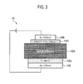
- the solar cell 10 is formed by stacking a semiconductor layer 10A, a front electrode layer 10B, a first electrode layer 10C, a second electrode layer 10D and a back electrode layer 10E, as shown in Fig. 3 .
- the semiconductor layer 10A is formed from a 1-mmt-thick ZnO substrate (in (0001) orientation), and the front electrode 10B is formed from Au with a thickness of 100 nm.
- the first electrode layer 10C is formed from a 100-nm-thick PEDOT-PSS (a conductive polymer made by H. C. Starck GmbH).
- the second electrode layer 10D is a metallic electrode layer for ohmic contact which is formed from Ti with a thickness of 40 nm.
- the back electrode layer 10E is formed from Au with a thickness of 100 nm.
- first electrode layer 10C and the semiconductor layer 10A are joined together with a Schottky junction interface in between, and the second electrode layer 10D and the semiconductor layer 10A are joined together by ohmic contact.
- the solar cell 10 is formed in a way that: once incident light hits the semiconductor layer 10A via the front electrode layer 10B and the first electrode layer 10C, electrons in a valence band jump to a conduction band in the semiconductor layer 10A, and photocarriers (electrons and holes) are thereby generated; photocarrier separation occurs due to built-in potential difference (diffusion potential difference) which exists in the semiconductor layer 10A near the Schottky junction interface; and thereby photovoltaic effects take place.
- the light energy of visible light is less than the bandgap between the conduction band and the valence band in the semiconductor layer 10A formed from the ZnO substrate. For this reason, no photovoltaic effects take place when the visible light is incident.
- the Schottky solar electron 10 shown in Fig. 3 has a problem of poor power generation efficiency with the sunlight including a large amount of the visible light.
- An object of the present invention is to provide a Schottky solar cell having fine power generation efficiency with the sunlight including a large amount of the visible light, and a method of manufacturing the same.
- a first feature of the present invention is summarized as a solar cell including a first electrode layer, a semiconductor layer and a second electrode layer which are stacked, in which the first electrode layer is placed on a light-irradiated surface side of the semiconductor layer, the first electrode layer and the semiconductor layer are joined together with a Schottky junction interface in between, the second electrode layer is placed on an opposite side of the semiconductor layer from the light-irradiated surface, the second electrode layer and the semiconductor layer are joined together in ohmic contact with each other, and the first electrode layer includes a visible light absorbing material.
- a solar cell 1 and a method of manufacturing the solar cell 1 of a first embodiment of the present invention.
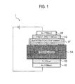
- the solar cell 10 of the embodiment is formed by stacking a semiconductor layer 1A, a front electrode layer 1B, a first electrode layer 1C/1F, a second electrode layer 1D and a back electrode layer 1E.
- the semiconductor layer 1A is formed from a 1-mmt-thick ZnO substrate (in (0001) orientation), for example.
- the front electrode 1B is formed from Au with a thickness of 100 nm, for example.
- the back electrode layer 1E is formed from Au with a thickness of 100 nm, for example.
- the second electrode layer 1D is a metallic electrode layer for ohmic contact, which is formed from Ti with a thickness of 40 nm, for example. To put it specifically, the second electrode layer 1D is placed on an opposite side of the semiconductor layer 10A from the light-irradiated surface, and is formed in ohmic contact with the semiconductor layer 1A.
- the first electrode layer 1C/1F is placed on a light-irradiated surface side of the semiconductor layer 10A, and is formed with a Schottky barrier between the first electrode layer 1C/1F and the semiconductor layer 10A.
- the first electrode layer 1C/1F includes a 100-nm-thick PEDOT-PSS (a conductive polymer made by H. C. Starck GmbH) layer 1C and a 40-nm-thick PEDOT-PSS (a conductive polymer made by H. C. Starck GmbH) layer 1F.
- PEDOT-PSS a conductive polymer made by H. C. Starck GmbH
- 40-nm-thick PEDOT-PSS a conductive polymer made by H. C. Starck GmbH
- the layer IF is formed to include a visible light absorbing material.
- the layer IF is formed to contain silicon microparticles (nanosilicon) as the visible light absorbing material.
- the silicon microparticles have a characteristic that "a bandgap between a conduction band and a valence band varies depending on the grain size of the silicon microparticles.” For example, when the grain size is “5 nm,” the bandgap is “2.0 eV.” When the grain size is “3 nm,” the bandgap is "2.5 eV.”
- a range of wavelengths (light energy) of the incident light which is absorbable into the layer 1 can be adjusted by changing the grain size of the silicon microparticles as the visible light absorbing material to be included in the layer 1.
- the solar cell 10 is formed in a way that: once the incident light hits the semiconductor layer 10A via the front electrode layer 10B and the first electrode layer 10C, electrons in a valence band jump to a conduction band in the semiconductor layer 10A, and photocarriers (electrons and holes) are thereby generated; photocarrier separation occurs due to built-in potential difference (diffusion potential difference) which exists in the semiconductor layer 10A near the Schottky junction interface; and thereby photovoltaic effects take place.
- the solar cell 1 is formed in a way that: once the incident light hits the silicon microparticles in the layer 1C via the front electrode layer 10B and the first electrode layer 10C, electrons in a valence band jump to a conduction band in the silicon microparticles, and photocarriers (electrons and holes) are thereby generated; photocarrier separation occurs due to built-in potential difference (diffusion potential difference) which exists in the semiconductor layer 10A near the Schottky junction interface; and thereby photovoltaic effects take place.
- the silicon microparticles be subjected to a termination treatment.
- the termination treatment improves the solubility of the silicon microparticles to the PEDOT-PSS solution to a large extent, and accordingly makes it possible to form the PEDOT-PSS layer IF containing the silicon microparticles with high homogeneity.
- the termination treatment increases the stability in the atmosphere to a large extent, and accordingly makes it possible to extend the life of the solar cell 1 of the embodiment.
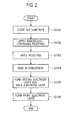
- a semiconductor substrate constituting the semiconductor layer 1A is cleaned in step S101.
- a ZnO substrate (zinc oxide single-crystal substrate) in (0001) orientation made by Tokyo Denpa Co., Ltd., is subj ected to ultrasonic cleaning with ethanol for 10 minutes, and is then subjected to ultrasonic cleaning with acetone for 10 minutes. Subsequently, the ZnO substrate is subjected to a cleaning process using a UV ozone cleaner for 10 minutes.
- step S102 a first conductive polymer including the visible light absorbing material is applied to the ZnO substrate.
- a solution is prepared by mixing PEDOT-PSS, which is the conductive polymer made by H. C. Starck GmbH, and a toluene solution of decene-terminated nanosilicon in a proportion of 30 to 70 in mass percentage. This solution is applied to the aforementioned ZnO substrate by spin coating.
- step S103 a second conductive polymer is applied to a light-irradiated surface side of the first conductive polymer applied in step S102.
- PEDOT-PSS which is the conductive polymer made by H. C. Starck GmbH
- a spinning condition is set to 5000 rpm per 30 seconds.
- step S104 a baking process is performed in atmosphere immediately after the completion of step S103.
- a temperature profile is set, for example, to a sequence of 50°C (for 10 minutes), 80°C (for 10 minutes), 150°C (for 10 minutes), 190°C (for 10 minutes), and then slow cooling to normal temperature.
- the second electrode layer 1D and the back electrode layer 1E are formed on the opposite side of the semiconductor layer (ZnO substrate) from the light-irradiated surface.
- the second electrode layer 1D and the back electrode layer 1E are formed by sputtering.
- step S106 the front electrode layer 1B is formed on a light-irradiated surface side of the second conductive polymer applied in step S103.
- step S105 the ZnO substrate is taken out into atmosphere. Subsequently, a metal mask having a punched-out circular pattern with a diameter of 0.2 mm is attached onto the PEDOT-PSS applied in step S103, and the front electrode layer 1B is formed on the metal mask by sputtering.
- the metal mask is removed, and the PEDOT-PSS with sides of approximately 0.3 mm around the front electrode layer 1B is mechanically removed using tweezers.
- the solar cell 1 of the first embodiment of the present invention is capable of obtaining photovoltaic power using the visible light, and is capable of enhancing effects of power generation using the sunlight including a large amount of the visible light.
- the photovoltaic power of the solar cell 10 of Comparative Example 1 and the photovoltaic power of the solar cell 1 of Example 1 were measured regarding cases of irradiation with LED lamps having a red wavelength (660 nm), a green wavelength (525 nm), a blue wavelength (470 nm) and an ultraviolet wavelength (365 nm), respectively.
- the solar cell 1 used in Example 1 had the structure shown in Fig. 1 and was manufactured by the manufacturing method shown in Fig. 2 .
- the solar cell 10 of the conventional example 1 had the structure shown in Fig. 3 and was manufactured by the manufacturing method shown in Fig. 2 except the processing in step S102.
- Table 1 shows the photovoltaic power obtained from the experiment.
- the solar cell 1 of Example 1 using the conductive polymer including the visible light absorbing material is capable of obtain photovoltaic power from the visible light.
- the solar cell and the method of manufacturing the same of the present invention are useful since they are capable of enhancing power generation efficiency with the sunlight including a large amount of the visible light.
Landscapes
- Chemical & Material Sciences (AREA)
- Inorganic Chemistry (AREA)
- Physics & Mathematics (AREA)
- Electromagnetism (AREA)
- Photovoltaic Devices (AREA)
Abstract
A solar cell (1) according to the invention is formed by stacking a first electrode layer (1C), a semiconductor layer (1A), and a second electrode layer (1D). The first electrode layer (1C) is placed on a light-irradiated surface side of the semiconductor layer (1A). The first electrode layer (1C) and the semiconductor layer (1A) are joined together with a Schottky junction interface in between. The second electrode layer (1D) is placed on an opposite side of the semiconductor layer (1A) from the light-irradiated surface. The second electrode layer (1D) and the semiconductor layer (1A) are joined together in ohmic contact with each other. The first electrode layer (1C) includes a visible light absorbing material.
Description
- The present invention relates to a solar cell and a method of manufacturing the same.
- Schottky solar cell structures have heretofore been known (
Patent Document 1 and Non-patent Document 1). - For example, a structure of a Schottky
solar cell 10 shown inFig. 3 has been known. Specifically, thesolar cell 10 is formed by stacking asemiconductor layer 10A, afront electrode layer 10B, afirst electrode layer 10C, asecond electrode layer 10D and aback electrode layer 10E, as shown inFig. 3 . - In the example shown in
Fig. 3 , thesemiconductor layer 10A is formed from a 1-mmt-thick ZnO substrate (in (0001) orientation), and thefront electrode 10B is formed from Au with a thickness of 100 nm. - In addition, the
first electrode layer 10C is formed from a 100-nm-thick PEDOT-PSS (a conductive polymer made by H. C. Starck GmbH). - The
second electrode layer 10D is a metallic electrode layer for ohmic contact which is formed from Ti with a thickness of 40 nm. Theback electrode layer 10E is formed from Au with a thickness of 100 nm. - It should be noted that the
first electrode layer 10C and thesemiconductor layer 10A are joined together with a Schottky junction interface in between, and thesecond electrode layer 10D and thesemiconductor layer 10A are joined together by ohmic contact. - The
solar cell 10 is formed in a way that: once incident light hits thesemiconductor layer 10A via thefront electrode layer 10B and thefirst electrode layer 10C, electrons in a valence band jump to a conduction band in thesemiconductor layer 10A, and photocarriers (electrons and holes) are thereby generated; photocarrier separation occurs due to built-in potential difference (diffusion potential difference) which exists in thesemiconductor layer 10A near the Schottky junction interface; and thereby photovoltaic effects take place. - It should be noted that when the light energy of the incident light is less than the bandgap between the conduction band and the valence band in the
semiconductor layer 10A, no such photovoltaic effects take place because: in thesemiconductor layer 10A, no electrons in the valence band can jump to the conduction band; and thesemiconductor layer 10A accordingly cannot absorb the incident light. - [PTL 1] Japanese Patent Application Publication No.
2010-219399 - [NPL 1] APPLIED PHYSICS LETTERS 93, 12309(2008)
- In this respect, in the structure of the Schottky
solar electron 10 shown inFig. 3 , the light energy of visible light is less than the bandgap between the conduction band and the valence band in thesemiconductor layer 10A formed from the ZnO substrate. For this reason, no photovoltaic effects take place when the visible light is incident. - As a result, the Schottky
solar electron 10 shown inFig. 3 has a problem of poor power generation efficiency with the sunlight including a large amount of the visible light. - The present invention has been made with the foregoing problem taken into consideration. An object of the present invention is to provide a Schottky solar cell having fine power generation efficiency with the sunlight including a large amount of the visible light, and a method of manufacturing the same.
- A first feature of the present invention is summarized as a solar cell including a first electrode layer, a semiconductor layer and a second electrode layer which are stacked, in which the first electrode layer is placed on a light-irradiated surface side of the semiconductor layer, the first electrode layer and the semiconductor layer are joined together with a Schottky junction interface in between, the second electrode layer is placed on an opposite side of the semiconductor layer from the light-irradiated surface, the second electrode layer and the semiconductor layer are joined together in ohmic contact with each other, and the first electrode layer includes a visible light absorbing material.
-
- [
Fig. 1 ]
Fig. 1 is a diagram showing a structure of a solar cell of a first embodiment of the present invention. - [
Fig. 2 ]
Fig. 2 is a flowchart showing an example of a method of manufacturing a solar cell of the first embodiment of the present invention. - [
Fig. 3 ]
Fig. 3 is a diagram showing a structure of a solar cell of a conventional technique. - Referring to
Fig. 1 , descriptions will be provided for asolar cell 1 and a method of manufacturing thesolar cell 1 of a first embodiment of the present invention. - Specifically, as shown in
Fig. 1 , thesolar cell 10 of the embodiment is formed by stacking a semiconductor layer 1A, afront electrode layer 1B, afirst electrode layer 1C/1F, asecond electrode layer 1D and aback electrode layer 1E. - The semiconductor layer 1A is formed from a 1-mmt-thick ZnO substrate (in (0001) orientation), for example.
- The
front electrode 1B is formed from Au with a thickness of 100 nm, for example. Theback electrode layer 1E is formed from Au with a thickness of 100 nm, for example. - The
second electrode layer 1D is a metallic electrode layer for ohmic contact, which is formed from Ti with a thickness of 40 nm, for example. To put it specifically, thesecond electrode layer 1D is placed on an opposite side of thesemiconductor layer 10A from the light-irradiated surface, and is formed in ohmic contact with the semiconductor layer 1A. - The
first electrode layer 1C/1F is placed on a light-irradiated surface side of thesemiconductor layer 10A, and is formed with a Schottky barrier between thefirst electrode layer 1C/1F and thesemiconductor layer 10A. - For example, the
first electrode layer 1C/1F includes a 100-nm-thick PEDOT-PSS (a conductive polymer made by H. C. Starck GmbH)layer 1C and a 40-nm-thick PEDOT-PSS (a conductive polymer made by H. C. Starck GmbH)layer 1F. - In this respect, the layer IF is formed to include a visible light absorbing material. For example, the layer IF is formed to contain silicon microparticles (nanosilicon) as the visible light absorbing material.
- It should be noted that the silicon microparticles have a characteristic that "a bandgap between a conduction band and a valence band varies depending on the grain size of the silicon microparticles." For example, when the grain size is "5 nm," the bandgap is "2.0 eV." When the grain size is "3 nm," the bandgap is "2.5 eV."
- Accordingly, a range of wavelengths (light energy) of the incident light which is absorbable into the
layer 1 can be adjusted by changing the grain size of the silicon microparticles as the visible light absorbing material to be included in thelayer 1. - The
solar cell 10 is formed in a way that: once the incident light hits thesemiconductor layer 10A via thefront electrode layer 10B and thefirst electrode layer 10C, electrons in a valence band jump to a conduction band in thesemiconductor layer 10A, and photocarriers (electrons and holes) are thereby generated; photocarrier separation occurs due to built-in potential difference (diffusion potential difference) which exists in thesemiconductor layer 10A near the Schottky junction interface; and thereby photovoltaic effects take place. - Likewise, the
solar cell 1 is formed in a way that: once the incident light hits the silicon microparticles in thelayer 1C via thefront electrode layer 10B and thefirst electrode layer 10C, electrons in a valence band jump to a conduction band in the silicon microparticles, and photocarriers (electrons and holes) are thereby generated; photocarrier separation occurs due to built-in potential difference (diffusion potential difference) which exists in thesemiconductor layer 10A near the Schottky junction interface; and thereby photovoltaic effects take place. - In this respect, it is desirable that the silicon microparticles be subjected to a termination treatment. In this formation, the termination treatment improves the solubility of the silicon microparticles to the PEDOT-PSS solution to a large extent, and accordingly makes it possible to form the PEDOT-PSS layer IF containing the silicon microparticles with high homogeneity. Furthermore, in this formation, the termination treatment increases the stability in the atmosphere to a large extent, and accordingly makes it possible to extend the life of the
solar cell 1 of the embodiment. - Referring to
Fig. 2 , descriptions will be hereinbelow provided for an example of the method of manufacturing thesolar cell 1. - As shown in
Fig. 2 , a semiconductor substrate constituting the semiconductor layer 1A is cleaned in step S101. - For example, a ZnO substrate (zinc oxide single-crystal substrate) in (0001) orientation, made by Tokyo Denpa Co., Ltd., is subj ected to ultrasonic cleaning with ethanol for 10 minutes, and is then subjected to ultrasonic cleaning with acetone for 10 minutes. Subsequently, the ZnO substrate is subjected to a cleaning process using a UV ozone cleaner for 10 minutes.
- In step S102, a first conductive polymer including the visible light absorbing material is applied to the ZnO substrate.
- For example, a solution is prepared by mixing PEDOT-PSS, which is the conductive polymer made by H. C. Starck GmbH, and a toluene solution of decene-terminated nanosilicon in a proportion of 30 to 70 in mass percentage. This solution is applied to the aforementioned ZnO substrate by spin coating.
- In step S103, a second conductive polymer is applied to a light-irradiated surface side of the first conductive polymer applied in step S102.
- For example, PEDOT-PSS, which is the conductive polymer made by H. C. Starck GmbH, is applied to the light-irradiated surface side of the solution applied in the step S102 by spin coating. Here, a spinning condition is set to 5000 rpm per 30 seconds.
- In step S104, a baking process is performed in atmosphere immediately after the completion of step S103. In this respect, a temperature profile is set, for example, to a sequence of 50°C (for 10 minutes), 80°C (for 10 minutes), 150°C (for 10 minutes), 190°C (for 10 minutes), and then slow cooling to normal temperature.
- In step S105, the
second electrode layer 1D and theback electrode layer 1E are formed on the opposite side of the semiconductor layer (ZnO substrate) from the light-irradiated surface. For example, thesecond electrode layer 1D and theback electrode layer 1E are formed by sputtering. - In step S106, the
front electrode layer 1B is formed on a light-irradiated surface side of the second conductive polymer applied in step S103. - For example, after the completion of step S105, the ZnO substrate is taken out into atmosphere. Subsequently, a metal mask having a punched-out circular pattern with a diameter of 0.2 mm is attached onto the PEDOT-PSS applied in step S103, and the
front electrode layer 1B is formed on the metal mask by sputtering. - Thereafter, the metal mask is removed, and the PEDOT-PSS with sides of approximately 0.3 mm around the
front electrode layer 1B is mechanically removed using tweezers. - Since the first conductive polymer including the visible light absorbing material (for example, the PEDOT-PSS containing the nanosilicon) is not transparent to visible light, the
solar cell 1 of the first embodiment of the present invention is capable of obtaining photovoltaic power using the visible light, and is capable of enhancing effects of power generation using the sunlight including a large amount of the visible light. - Next, in order to make the effects of the present invention clearer, the photovoltaic power of the
solar cell 10 of Comparative Example 1 and the photovoltaic power of thesolar cell 1 of Example 1 were measured regarding cases of irradiation with LED lamps having a red wavelength (660 nm), a green wavelength (525 nm), a blue wavelength (470 nm) and an ultraviolet wavelength (365 nm), respectively. - It should be noted that the
solar cell 1 used in Example 1 had the structure shown inFig. 1 and was manufactured by the manufacturing method shown inFig. 2 . Meanwhile, thesolar cell 10 of the conventional example 1 had the structure shown inFig. 3 and was manufactured by the manufacturing method shown inFig. 2 except the processing in step S102. - Here, Table 1 shows the photovoltaic power obtained from the experiment.
[Table 1] Dark State Red Green Blue Ultraviolet Comparative Example 1 0.00 V 0.00 V 0.00 V 0.02 V 0.45 V Example 1 0.00 V 0.01 V 0.05 V 0.20 V 0.35 V - As shown in Table 1, it is learned that the
solar cell 1 of Example 1 using the conductive polymer including the visible light absorbing material is capable of obtain photovoltaic power from the visible light. - Hereinabove, the present invention has been described in detail by use of the foregoing embodiments. However, it is apparent to those skilled in the art that the present invention should not be limited to the embodiments described in the specification. The present invention can be implemented as an altered or modified embodiment without departing from the spirit and scope of the present invention, which are determined by the description of the scope of claims. Therefore, the description of the specification is intended for illustrative explanation only and does not impose any limited interpretation on the present invention.
- Note that the entire content of Japanese Patent Application No.
2011-268787 (filed on December 8, 2011 - As described above, the solar cell and the method of manufacturing the same of the present invention are useful since they are capable of enhancing power generation efficiency with the sunlight including a large amount of the visible light.
Claims (5)
- A solar cell comprising a first electrode layer, a semiconductor layer and a second electrode layer which are stacked, wherein
the first electrode layer is placed on a light-irradiated surface side of the semiconductor layer,
the first electrode layer and the semiconductor layer are joined together with a Schottky junction interface in between,
the second electrode layer is placed on an opposite side of the semiconductor layer from the light-irradiated surface,
the second electrode layer and the semiconductor layer are joined together in ohmic contact with each other, and
the first electrode layer includes a visible light absorbing material. - The solar cell of claim 1, wherein the visible light absorbing material is silicon microparticles.
- The solar cell of claim 2, wherein the silicon microparticles are subjected to a termination treatment.
- The solar cell of claim 1, wherein the first electrode layer is formed from a conductive polymer.
- A method of manufacturing a solar cell, comprising the steps of:applying a first conductive polymer including a visible light absorbing material to a light-irradiated surface side of a semiconductor layer;applying a second conductive polymer to a light-irradiated surface side of the first conductive polymer; andforming an electrode layer on an opposite side of the semiconductor layer from the light-irradiated surface.
Applications Claiming Priority (2)
| Application Number | Priority Date | Filing Date | Title |
|---|---|---|---|
| JP2011268787A JP2013120878A (en) | 2011-12-08 | 2011-12-08 | Solar cell and solar cell manufacturing method |
| PCT/JP2012/081547 WO2013084954A1 (en) | 2011-12-08 | 2012-12-05 | Solar cell and solar cell manufacturing method |
Publications (2)
| Publication Number | Publication Date |
|---|---|
| EP2790229A1 true EP2790229A1 (en) | 2014-10-15 |
| EP2790229A4 EP2790229A4 (en) | 2015-07-08 |
Family
ID=48574312
Family Applications (1)
| Application Number | Title | Priority Date | Filing Date |
|---|---|---|---|
| EP12856509.0A Withdrawn EP2790229A4 (en) | 2011-12-08 | 2012-12-05 | SOLAR CELL AND METHOD FOR MANUFACTURING SOLAR CELL |
Country Status (5)
| Country | Link |
|---|---|
| US (1) | US20140326303A1 (en) |
| EP (1) | EP2790229A4 (en) |
| JP (1) | JP2013120878A (en) |
| CN (1) | CN103975444A (en) |
| WO (1) | WO2013084954A1 (en) |
Families Citing this family (1)
| Publication number | Priority date | Publication date | Assignee | Title |
|---|---|---|---|---|
| US10608184B2 (en) * | 2012-12-03 | 2020-03-31 | The University Of Akron | Organic polymer photo device with broadband response and increased photo-responsitivity |
Family Cites Families (6)
| Publication number | Priority date | Publication date | Assignee | Title |
|---|---|---|---|---|
| JP2006237283A (en) * | 2005-02-25 | 2006-09-07 | Nippon Paint Co Ltd | Organic solar cell and manufacturing method thereof |
| JP4362635B2 (en) * | 2007-02-02 | 2009-11-11 | ローム株式会社 | ZnO-based semiconductor element |
| KR20090047107A (en) * | 2007-11-07 | 2009-05-12 | 한양대학교 산학협력단 | Method for manufacturing solar cell using semiconductor nanoparticles formed in polymer thin film |
| JP2010050432A (en) * | 2008-07-24 | 2010-03-04 | Rohm Co Ltd | Ultraviolet detection apparatus |
| JP2010205891A (en) * | 2009-03-03 | 2010-09-16 | Rohm Co Ltd | Semiconductor device |
| JP5562568B2 (en) | 2009-03-18 | 2014-07-30 | 株式会社東芝 | Schottky type solar cell and manufacturing method |
-
2011
- 2011-12-08 JP JP2011268787A patent/JP2013120878A/en not_active Withdrawn
-
2012
- 2012-12-05 WO PCT/JP2012/081547 patent/WO2013084954A1/en not_active Ceased
- 2012-12-05 EP EP12856509.0A patent/EP2790229A4/en not_active Withdrawn
- 2012-12-05 US US14/361,912 patent/US20140326303A1/en not_active Abandoned
- 2012-12-05 CN CN201280059996.2A patent/CN103975444A/en active Pending
Also Published As
| Publication number | Publication date |
|---|---|
| CN103975444A (en) | 2014-08-06 |
| US20140326303A1 (en) | 2014-11-06 |
| EP2790229A4 (en) | 2015-07-08 |
| JP2013120878A (en) | 2013-06-17 |
| WO2013084954A1 (en) | 2013-06-13 |
Similar Documents
| Publication | Publication Date | Title |
|---|---|---|
| CN103703567B (en) | Solar cell, solar cell manufacturing method, and solar cell module | |
| KR101220304B1 (en) | Up conversion oxide fluorescent composition for solar cell and method of fabrication of high efficiency solar cell using thereof | |
| JP5694620B1 (en) | Crystalline silicon solar cell manufacturing method and crystalline silicon solar cell module manufacturing method | |
| CN1534798A (en) | Multilayer Photovoltaic Elements | |
| JP2010050356A (en) | Process for manufacturing heterojunction solar cell and heterojunction solar cell | |
| WO2010025291A3 (en) | Four terminal multi-junction thin film photovoltaic device and method | |
| KR100946797B1 (en) | Manufacturing method of high efficiency solar cell using laser | |
| KR20120082663A (en) | Solar cell and method for manufacturing the same | |
| CN104300032A (en) | Single crystal silicon solar ion implantation technology | |
| CN117352563A (en) | Solar cells and photovoltaic modules | |
| TW201515244A (en) | Solar battery and solar battery module | |
| CN1220276C (en) | Laminated photoelectric element | |
| EP2720280A1 (en) | Photoelectric conversion element | |
| CN110073498B (en) | High photoelectric conversion efficiency solar cell and method for manufacturing high photoelectric conversion efficiency solar cell | |
| TW201440235A (en) | Back junction solar cell with reinforced emitter layer | |
| JP2015233027A (en) | PHOTOELECTRIC CONVERSION ELEMENT, METHOD FOR PRODUCING PHOTOELECTRIC CONVERSION ELEMENT, LAMINATE TYPE SOLID-STATE IMAGING ELEMENT | |
| US20140326303A1 (en) | Solar cell and method of manufacturing the same | |
| WO2021010127A1 (en) | Semiconductor device and solar battery and production method for semiconductor device | |
| JP6072904B2 (en) | Photovoltaic element and manufacturing method thereof | |
| KR101473697B1 (en) | Photoelectric device and method for fabricating the same | |
| KR101252815B1 (en) | Down conversion oxide fluorescent composition for solar cell and method of fabrication of high efficiency solar cell using thereof | |
| CN102191563A (en) | Preparation method of codoped silicon-base impurity intermediate belt material | |
| CN103956399B (en) | Silicon solar cell backboard and manufacturing method thereof | |
| WO2017017772A1 (en) | Photovoltaic power generation element and method for manufacturing same | |
| KR101939482B1 (en) | Silicon solar cell, and method for manufacturing same |
Legal Events
| Date | Code | Title | Description |
|---|---|---|---|
| PUAI | Public reference made under article 153(3) epc to a published international application that has entered the european phase |
Free format text: ORIGINAL CODE: 0009012 |
|
| 17P | Request for examination filed |
Effective date: 20140708 |
|
| AK | Designated contracting states |
Kind code of ref document: A1 Designated state(s): AL AT BE BG CH CY CZ DE DK EE ES FI FR GB GR HR HU IE IS IT LI LT LU LV MC MK MT NL NO PL PT RO RS SE SI SK SM TR |
|
| DAX | Request for extension of the european patent (deleted) | ||
| RA4 | Supplementary search report drawn up and despatched (corrected) |
Effective date: 20150605 |
|
| RIC1 | Information provided on ipc code assigned before grant |
Ipc: H01L 31/04 20140101AFI20150529BHEP |
|
| STAA | Information on the status of an ep patent application or granted ep patent |
Free format text: STATUS: THE APPLICATION IS DEEMED TO BE WITHDRAWN |
|
| 18D | Application deemed to be withdrawn |
Effective date: 20160105 |