EP2790225A1 - Method for manufacturing semiconductor device - Google Patents
Method for manufacturing semiconductor device Download PDFInfo
- Publication number
- EP2790225A1 EP2790225A1 EP12854962.3A EP12854962A EP2790225A1 EP 2790225 A1 EP2790225 A1 EP 2790225A1 EP 12854962 A EP12854962 A EP 12854962A EP 2790225 A1 EP2790225 A1 EP 2790225A1
- Authority
- EP
- European Patent Office
- Prior art keywords
- oxide film
- substrate
- main surface
- manufacturing
- semiconductor device
- Prior art date
- Legal status (The legal status is an assumption and is not a legal conclusion. Google has not performed a legal analysis and makes no representation as to the accuracy of the status listed.)
- Granted
Links
Images




Classifications
-
- H—ELECTRICITY
- H10—SEMICONDUCTOR DEVICES; ELECTRIC SOLID-STATE DEVICES NOT OTHERWISE PROVIDED FOR
- H10D—INORGANIC ELECTRIC SEMICONDUCTOR DEVICES
- H10D62/00—Semiconductor bodies, or regions thereof, of devices having potential barriers
- H10D62/80—Semiconductor bodies, or regions thereof, of devices having potential barriers characterised by the materials
- H10D62/83—Semiconductor bodies, or regions thereof, of devices having potential barriers characterised by the materials being Group IV materials, e.g. B-doped Si or undoped Ge
- H10D62/832—Semiconductor bodies, or regions thereof, of devices having potential barriers characterised by the materials being Group IV materials, e.g. B-doped Si or undoped Ge being Group IV materials comprising two or more elements, e.g. SiGe
- H10D62/8325—Silicon carbide
-
- H—ELECTRICITY
- H10—SEMICONDUCTOR DEVICES; ELECTRIC SOLID-STATE DEVICES NOT OTHERWISE PROVIDED FOR
- H10D—INORGANIC ELECTRIC SEMICONDUCTOR DEVICES
- H10D64/00—Electrodes of devices having potential barriers
- H10D64/01—Manufacture or treatment
- H10D64/011—Manufacture or treatment of electrodes ohmically coupled to a semiconductor
- H10D64/0111—Manufacture or treatment of electrodes ohmically coupled to a semiconductor to Group IV semiconductors
- H10D64/0115—Manufacture or treatment of electrodes ohmically coupled to a semiconductor to Group IV semiconductors to silicon carbide
-
- H—ELECTRICITY
- H10—SEMICONDUCTOR DEVICES; ELECTRIC SOLID-STATE DEVICES NOT OTHERWISE PROVIDED FOR
- H10D—INORGANIC ELECTRIC SEMICONDUCTOR DEVICES
- H10D64/00—Electrodes of devices having potential barriers
- H10D64/01—Manufacture or treatment
- H10D64/012—Manufacture or treatment of electrodes comprising a Schottky barrier to a semiconductor
- H10D64/0121—Manufacture or treatment of electrodes comprising a Schottky barrier to a semiconductor to Group IV semiconductors
- H10D64/0123—Manufacture or treatment of electrodes comprising a Schottky barrier to a semiconductor to Group IV semiconductors to silicon carbide
-
- H—ELECTRICITY
- H10—SEMICONDUCTOR DEVICES; ELECTRIC SOLID-STATE DEVICES NOT OTHERWISE PROVIDED FOR
- H10D—INORGANIC ELECTRIC SEMICONDUCTOR DEVICES
- H10D64/00—Electrodes of devices having potential barriers
- H10D64/01—Manufacture or treatment
- H10D64/013—Manufacture or treatment of electrodes having a conductor capacitively coupled to a semiconductor by an insulator
- H10D64/01366—Manufacture or treatment of electrodes having a conductor capacitively coupled to a semiconductor by an insulator the semiconductor being silicon carbide
-
- H—ELECTRICITY
- H10—SEMICONDUCTOR DEVICES; ELECTRIC SOLID-STATE DEVICES NOT OTHERWISE PROVIDED FOR
- H10D—INORGANIC ELECTRIC SEMICONDUCTOR DEVICES
- H10D64/00—Electrodes of devices having potential barriers
- H10D64/60—Electrodes characterised by their materials
- H10D64/64—Electrodes comprising a Schottky barrier to a semiconductor
-
- H—ELECTRICITY
- H10—SEMICONDUCTOR DEVICES; ELECTRIC SOLID-STATE DEVICES NOT OTHERWISE PROVIDED FOR
- H10D—INORGANIC ELECTRIC SEMICONDUCTOR DEVICES
- H10D8/00—Diodes
- H10D8/01—Manufacture or treatment
- H10D8/051—Manufacture or treatment of Schottky diodes
-
- H—ELECTRICITY
- H10—SEMICONDUCTOR DEVICES; ELECTRIC SOLID-STATE DEVICES NOT OTHERWISE PROVIDED FOR
- H10D—INORGANIC ELECTRIC SEMICONDUCTOR DEVICES
- H10D8/00—Diodes
- H10D8/60—Schottky-barrier diodes
-
- H—ELECTRICITY
- H10—SEMICONDUCTOR DEVICES; ELECTRIC SOLID-STATE DEVICES NOT OTHERWISE PROVIDED FOR
- H10D—INORGANIC ELECTRIC SEMICONDUCTOR DEVICES
- H10D62/00—Semiconductor bodies, or regions thereof, of devices having potential barriers
- H10D62/10—Shapes, relative sizes or dispositions of the regions of the semiconductor bodies; Shapes of the semiconductor bodies
- H10D62/102—Constructional design considerations for preventing surface leakage or controlling electric field concentration
- H10D62/103—Constructional design considerations for preventing surface leakage or controlling electric field concentration for increasing or controlling the breakdown voltage of reverse-biased devices
- H10D62/105—Constructional design considerations for preventing surface leakage or controlling electric field concentration for increasing or controlling the breakdown voltage of reverse-biased devices by having particular doping profiles, shapes or arrangements of PN junctions; by having supplementary regions, e.g. junction termination extension [JTE]
- H10D62/106—Constructional design considerations for preventing surface leakage or controlling electric field concentration for increasing or controlling the breakdown voltage of reverse-biased devices by having particular doping profiles, shapes or arrangements of PN junctions; by having supplementary regions, e.g. junction termination extension [JTE] having supplementary regions doped oppositely to or in rectifying contact with regions of the semiconductor bodies, e.g. guard rings with PN or Schottky junctions
-
- H—ELECTRICITY
- H10—SEMICONDUCTOR DEVICES; ELECTRIC SOLID-STATE DEVICES NOT OTHERWISE PROVIDED FOR
- H10D—INORGANIC ELECTRIC SEMICONDUCTOR DEVICES
- H10D62/00—Semiconductor bodies, or regions thereof, of devices having potential barriers
- H10D62/10—Shapes, relative sizes or dispositions of the regions of the semiconductor bodies; Shapes of the semiconductor bodies
- H10D62/102—Constructional design considerations for preventing surface leakage or controlling electric field concentration
- H10D62/112—Constructional design considerations for preventing surface leakage or controlling electric field concentration for preventing surface leakage due to surface inversion layers, e.g. by using channel stoppers
-
- H—ELECTRICITY
- H10—SEMICONDUCTOR DEVICES; ELECTRIC SOLID-STATE DEVICES NOT OTHERWISE PROVIDED FOR
- H10D—INORGANIC ELECTRIC SEMICONDUCTOR DEVICES
- H10D64/00—Electrodes of devices having potential barriers
- H10D64/60—Electrodes characterised by their materials
- H10D64/62—Electrodes ohmically coupled to a semiconductor
Definitions
- the present invention relates to a method for manufacturing a semiconductor device, and more particularly to a method for manufacturing a semiconductor device capable of achieving improved breakdown voltage characteristics.
- SBD Schottky barrier diode
- JBS junction barrier Schottky diode
- PTL 1 Japanese Patent Laying-Open No. 9-246573
- the present invention was made in view of the problems described above, and an object of the present invention is to provide a method for manufacturing a semiconductor device capable of achieving improved breakdown voltage characteristics.
- a method for manufacturing a semiconductor device of the present invention includes the steps of preparing a substrate made of silicon carbide and having a first conductivity type region formed to include one main surface, forming a second conductivity type region in a region including the main surface, forming an oxide film on the main surface across the first conductivity type region and the second conductivity type region, by heating the substrate having the second conductivity type region formed therein at a temperature of 1250°C or more, removing the oxide film to expose at least a part of the main surface, and forming a Schottky electrode in contact with the main surface that has been exposed by removing the oxide film.
- the present inventors conducted detailed studies of means for improving breakdown voltage characteristics of a semiconductor device, and arrived at the present invention based on the following findings.
- the present inventors found that, when forming an oxide film by heating a substrate in a method for manufacturing a semiconductor device, different rates of formation of the oxide film between a first conductivity type region and a second conductivity type region causes exaggerated roughness of an interface between a main surface of the substrate exposed by removing the oxide film, or the substrate, and the oxide film.
- the present inventors also found that, if the oxide film is formed by heating the substrate at a temperature of 1250°C or more, the rate of formation of the oxide film can be less dependent on the conductivity type to thereby reduce the roughness, to arrive at the present invention.
- the substrate is heated at a temperature of 1250°C or more in the step of forming the oxide film.
- the rate of formation of the oxide film can be less dependent on the conductivity type, to form the oxide film with suppressed variation in film thickness.
- the surface roughness of the main surface of the substrate exposed by removing the oxide film can be reduced, to obtain a satisfactory contact state between the substrate and the Schottky electrode formed on the main surface of the substrate. According to the method for manufacturing a semiconductor device of the present invention, therefore, by obtaining the satisfactory contact state between the substrate and the Schottky electrode, a method for manufacturing a semiconductor device capable of achieving improved breakdown voltage characteristics can be provided.
- the oxide film in the step of forming an oxide film, may be formed on the main surface by heating the substrate at a temperature of 1300°C or more. As such, variation in film thickness of the formed oxide film can be suppressed more effectively.
- the oxide film in the step of removing the oxide film, the oxide film may be removed to expose a part of the main surface.
- the Schottky electrode in the step of forming a Schottky electrode, the Schottky electrode may be formed in contact with the main surface that has been exposed by removing the oxide film and with the oxide film.
- the remaining oxide film can function as an electric field relaxation FP (Field Plate), to further improve the breakdown voltage characteristics of the semiconductor device.
- the step of further depositing an oxide film on this oxide film can be performed.
- the oxide film formed by heating the substrate and the oxide film deposited on this oxide film may be removed to expose a part of the main surface of the substrate. As such, the oxide film having a greater thickness can be left, to further improve the function of the oxide film as an electric field relaxation FP.
- the method for manufacturing a semiconductor device may further include the step of heating the substrate having the oxide film formed thereon in a nitrogen-containing atmosphere, before the step of removing the oxide film.
- an interface state of a region including the interface between the oxide film and the silicon carbide that forms the substrate can be reduced, to further improve the breakdown voltage characteristics of the semiconductor device.
- the oxide film having a thickness of 0.1 ⁇ m or more may be formed.
- the thickness of the oxide film can be set within a practically suitable range.
- the oxide film in the step of removing the oxide film, may be removed to expose the entire main surface.
- the semiconductor device without the oxide film functioning as an electric field relaxation FP can be readily manufactured.
- the Schottky electrode including at least one selected from the group consisting of Ti, W, Mo, Ni, Ta, Al and Au may be formed.
- various types of metals capable of making Schottky contact with the substrate can be employed as a metal that forms the Schottky electrode.
- a method for manufacturing a semiconductor device of the present invention a method for manufacturing a semiconductor device capable of achieving improved breakdown voltage characteristics can be provided.
- a method for manufacturing a semiconductor device according to a first embodiment which is one embodiment of the present invention is described.
- a substrate preparation step is performed.
- steps (S11) and (S 12) to be described below are performed to prepare a substrate 10 made of silicon carbide.
- a base substrate preparation step is performed.
- this step (S11) referring to Fig. 2 , an ingot made of 4H-SiC (not shown) is cut into a slice, for example, to prepare a base substrate 11 made of silicon carbide and having an n conductivity type.
- an epitaxial growth layer formation step is performed.
- this step (S12) referring to Fig. 2 , first, an electric field stop layer 12 having an n conductivity type is formed by epitaxial growth on a main surface 11A of base substrate 11. Then, a semiconductor layer 13 having an n conductivity type is similarly formed by epitaxial growth on a main surface of electric field stop layer 12 opposite to base substrate 11. As such, substrate 10 having a main surface 10A and formed of base substrate 11, electric field stop layer 12 and semiconductor layer 13 is prepared.
- step (S20) an ion implantation step is performed.
- this step (S20) referring to Fig. 3 , first, Al (aluminum) ions are implanted into semiconductor layer 13 as indicated with arrows in the figure, for example, to form p regions 15 having a p conductivity type. Then, Al ions are implanted into an area of semiconductor layer 13 which is closer to the outer edge than p regions 15, for example, to form guard ring regions 16 having a p conductivity type. Then, P (phosphorus) ions are implanted into an area of semiconductor layer 13 which is closer to the outer edge than guard ring regions 16, for example, to form a field stop region 17 having an n conductivity type.
- Al (aluminum) ions are implanted into semiconductor layer 13 as indicated with arrows in the figure, for example, to form p regions 15 having a p conductivity type.
- Al ions are implanted into an area of semiconductor layer 13 which is closer to the outer edge than p regions
- p regions 15 and guard ring regions 16 as p type (second conductivity type) regions, and field stop region 17 as an n type (first conductivity type) region are formed in a region including main surface 10A of substrate 10.
- p regions 15, guard ring regions 16 surrounding p regions 15, and field stop region 17 surrounding p regions 15 and guard ring regions 16 are formed in the region including main surface 10A of substrate 10.
- a region in semiconductor layer 13 in which neither of p regions 15, guard ring regions 16 and field stop region 17 is formed is a drift region 14, which forms an n type region together with field stop region 17.
- the ion implantations can be performed after a mask made of SiO2 (silicon dioxide) is formed on main surface 10A of substrate 10, for example, to form the impurity regions in desired positions in semiconductor layer 13, as shown in Fig. 3 .
- a mask made of SiO2 silicon dioxide
- step (S30) an activation annealing step is performed.
- substrate 10 is heated at a temperature of 1700°C for 30 minutes, for example, to activate the impurities introduced in the step (S20). As such, desired carriers are generated in the regions where the impurities have been introduced.
- an oxide film formation step is performed.
- an oxide film 20 made of SiO 2 (silicon dioxide) is formed, for example, to cover main surface 10A of substrate 10.
- substrate 10 is heated at a temperature of 1250°C or more in an oxygen-containing atmosphere, to form oxide film 20 on main surface 10A across drift region 14 and field stop region 17 as n type regions, and p regions 15 and guard ring regions 16 as p type regions.
- a nitriding process step is performed.
- substrate 10 is heated in an atmosphere containing a gas including nitrogen atoms such as NO (nitric oxide), NO 2 (nitrogen dioxide) or N 2 O (nitrous oxide), for example, to introduce the nitrogen atoms into a region including an interface between oxide film 20 and the silicon carbide that forms substrate 10.
- a gas including nitrogen atoms such as NO (nitric oxide), NO 2 (nitrogen dioxide) or N 2 O (nitrous oxide
- this step (S50) is not an essential step of the method for manufacturing a semiconductor device of the present invention, if this step is performed, an interface state of the region including the interface between oxide film 20 and the silicon carbide that forms substrate 10 can be reduced, to further improve breakdown voltage characteristics of a JBS 1.
- SiO 2 silicon dioxide
- CVD Chemical Vapor Deposition
- an ohmic electrode formation step is performed.
- a metallic film made of Ni (not shown) is formed by sputtering, for example, on a main surface 11B of base substrate 11 opposite to main surface 11A. Then, the metallic film is heated at 1000°C, for example, to silicidize at least a part of the metallic film. As such, an ohmic electrode 30 electrically connected to base substrate 11 is formed.
- a pad electrode formation step is performed.
- a pad electrode 40 made of a conductor such as NiAu and TiAu is formed on ohmic electrode 30 by evaporation, for example.
- oxide film 20 is removed to expose a part of main surface 10A of substrate 10. Specifically, oxide film 20 is removed to expose a part of drift region 14 and p regions 15, as shown in Fig. 6 , by dry etching such as RIE (Reactive Ion Etching) and wet etching with hydrofluoric acid, for example. If SiO 2 (silicon dioxide) is further deposited on oxide film 20 that has been formed by thermal oxidation in the step (S40) as described above, in this step (S80), oxide film 20 formed by thermal oxidation and the SiO 2 (silicon dioxide) deposited on oxide film 20 are removed to expose a part of main surface 10A of substrate 10.
- RIE Reactive Ion Etching
- a Schottky electrode formation step is performed.
- a Schottky electrode 50 is formed in contact with main surface 10A of substrate 10 that has been exposed by removing oxide film 20 in the step (S80) and with oxide film 20.
- a metallic film made of Ti or TiAl is formed on main surface 10A and oxide film 20 by sputtering, for example.
- the metallic film is heated at 500°C, for example, to silicidize at least a part of the metallic film, to form Schottky electrode 50 having thickness of 0.1 ⁇ m or more in contact with main surface 10A, across one of oxide films 20 and the other oxide film 20 with the contact portion interposed therebetween.
- Schottky electrode 50 including at least one metal selected from the group consisting of Ti, W, Mo, Ni, Ta, Al and Au may be formed, or Schottky electrode 50 made of one metal selected from the group of metals above may be formed.
- Schottky electrode 50 made of an alloy of two or more metals selected from the group of metals above such as TiW or TiTa may be formed.
- Schottky electrode 50 having a metallic film made of one metal selected from the group of metals above and a metallic film made of another metal laminated one above the other may be formed.
- Schottky electrode 50 made of nitride of one metal selected from the group of metals above such as TiN may be formed.
- various types of materials capable of making Schottky contact with substrate 10 can be employed as a material for Schottky electrode 50.
- a wire formation step is performed.
- a wire 60 made of a conductor such as Al is formed to surround Schottky electrode 50 by evaporation, for example.
- a passivation film formation step is performed.
- a passivation film 70 made of SiO 2 (silicon dioxide) is formed on oxide film 20 and wire 60 by CVD, for example.
- substrate 10 is heated at a temperature of 1250°C or more in the step (S40).
- the rate of formation of oxide film 20 can be less dependent on the conductivity type, to form oxide film 20 with suppressed variation in film thickness.
- the surface roughness of main surface 10A of substrate 10 exposed by removing oxide film 20 can be reduced, to obtain a satisfactory contact state between substrate 10 and Schottky electrode 50 formed on main surface 10A of substrate 10.
- JBS 1 with improved breakdown voltage characteristics can be manufactured.
- oxide film 20 is removed to expose a part of main surface 10A of substrate 10, and Schottky electrode 50 is formed in contact with main surface 10 that has been exposed by removing oxide film 20, and with remaining oxide film 20.
- remaining oxide film 20 can function as an electric field relaxation FP (Field Plate) to avoid electric field concentration at opposing ends of Schottky electrode 50, thereby further improving the breakdown voltage characteristics of JBS 1.
- oxide film 20 is formed by heating substrate 10 at 1250°C or more as described above. As such, the roughness of the interface between substrate 10 and oxide film 20 can be reduced, to further improve the function of oxide film 20 as an electric field relaxation FP.
- oxide film 20 having a greater thickness can be left, to further improve the function of oxide film 20 as an electric field relaxation FP.
- oxide film 20 having thickness of 0.1 ⁇ m or more may be formed. It is preferable to set the thickness of oxide film 20 within such a practically suitable range, namely, within a range required to avoid breakdown of oxide film 20.
- the method for manufacturing a semiconductor device according to this embodiment is basically implemented similarly to that as discussed above with regard to the semiconductor device according to the first embodiment, and provides similar effects.
- the method for manufacturing a semiconductor device according to this embodiment is different from the method for manufacturing a semiconductor device according to the first embodiment in that the oxide film is removed to expose the entire main surface of the substrate in the oxide film removal step.
- the method for manufacturing a semiconductor device according to this embodiment will be described. Referring to Fig. 1 , first, the steps (S10) to (S70) are performed similarly to the first embodiment. The step (S50) is omitted in this embodiment.
- the oxide film removal step is performed.
- oxide film 20 is removed to expose the entire main surface 10A of substrate 10.
- the Schottky electrode formation step is performed.
- Schottky electrode 50 is formed in contact with main surface 10A that has been exposed by removing oxide film 20 in the step (S80) similarly to the first embodiment.
- step (S100) the wire formation step is performed.
- this step (S100) referring to Fig. 11 , wire 60 is formed to surround Schottky electrode 50 similarly to the first embodiment.
- step (S110) the passivation film formation step is performed.
- this step (S110) referring to Fig. 11 , passivation film 70 is formed on main surface 10A of substrate 10 and wire 60.
- a JBS 2 is manufactured, and the method for manufacturing a semiconductor device according to this embodiment is completed.
- substrate 10 is heated at a temperature of 1250°C or more in the step (S40).
- the rate of formation of oxide film 20 can be less dependent on the conductivity type, to form oxide film 20 with suppressed variation in film thickness.
- the surface roughness of main surface 10A of substrate 10 exposed by removing oxide film 20 can be reduced, to obtain a satisfactory contact state between substrate 10 and Schottky electrode 50 formed on main surface 10A of substrate 10.
- JBS 1 with improved breakdown voltage characteristics can be manufactured.
- oxide film 20 may be formed on main surface 10A of substrate 10 by heating substrate 10 at a temperature of 1300°C or more. As such, variation in film thickness of oxide film 20 can be suppressed more effectively. As a result, the contact between substrate 10 and Schottky electrode 50 can be further enhanced, to further improve the breakdown voltage characteristics of JBSs 1 and 2.
- the methods for manufacturing a semiconductor device according to the first and second embodiments of the present invention are only directed to the JBSs in which p regions 15 are formed in the region including main surface 10A in contact with Schottky electrode 50, the method for manufacturing a semiconductor device of the present invention is not limited as such. Namely, the method for manufacturing a semiconductor device of the present invention can be employed in manufacturing a SBD in which p regions 15 are not formed. As such, the roughness of the interface between oxide film 20 and substrate 10 can be reduced, to manufacture a SBD with improved characteristics of oxide film 20 as an electric field relaxation FP.
- Fig. 12 illustrates the effect of heating temperature on variation in film thickness of the oxide film.
- the abscissa represents the heating temperature (°C) of the substrate
- the left ordinate represents the thickness ( ⁇ ) of the oxide film
- the right ordinate represents average variation (%) in film thickness of the oxide film.
- the average variation as used herein refers to a standard deviation ( ⁇ ) of the film thickness of the oxide film.
- the method for manufacturing a semiconductor device of the present invention is applicable particularly advantageously to a method for manufacturing a semiconductor device required to achieve improved breakdown voltage characteristics.
Landscapes
- Electrodes Of Semiconductors (AREA)
Abstract
Description
- The present invention relates to a method for manufacturing a semiconductor device, and more particularly to a method for manufacturing a semiconductor device capable of achieving improved breakdown voltage characteristics.
- Semiconductor devices such as a Schottky barrier diode (SBD) and a junction barrier Schottky diode (JBS) have a structure in which a Schottky electrode is formed on a substrate. To improve breakdown voltage characteristics of the SBD and JBS, a satisfactory contact state between the substrate and the Schottky electrode needs to be secured. For this reason, it has been proposed to form an oxide film in advance on a substrate surface on which a Schottky electrode is to be formed, and to form the Schottky electrode on the clean substrate surface obtained by removing the oxide film (see Japanese Patent Laying-Open No.
9-246573 - PTL 1: Japanese Patent Laying-Open No.
9-246573 - To further improve the breakdown voltage characteristics of the SBD and JBS, there is a need for a manufacturing method capable of further enhancing the contact state between the substrate and the Schottky electrode.
- The present invention was made in view of the problems described above, and an object of the present invention is to provide a method for manufacturing a semiconductor device capable of achieving improved breakdown voltage characteristics.
- A method for manufacturing a semiconductor device of the present invention includes the steps of preparing a substrate made of silicon carbide and having a first conductivity type region formed to include one main surface, forming a second conductivity type region in a region including the main surface, forming an oxide film on the main surface across the first conductivity type region and the second conductivity type region, by heating the substrate having the second conductivity type region formed therein at a temperature of 1250°C or more, removing the oxide film to expose at least a part of the main surface, and forming a Schottky electrode in contact with the main surface that has been exposed by removing the oxide film.
- The present inventors conducted detailed studies of means for improving breakdown voltage characteristics of a semiconductor device, and arrived at the present invention based on the following findings.
- The present inventors found that, when forming an oxide film by heating a substrate in a method for manufacturing a semiconductor device, different rates of formation of the oxide film between a first conductivity type region and a second conductivity type region causes exaggerated roughness of an interface between a main surface of the substrate exposed by removing the oxide film, or the substrate, and the oxide film. The present inventors also found that, if the oxide film is formed by heating the substrate at a temperature of 1250°C or more, the rate of formation of the oxide film can be less dependent on the conductivity type to thereby reduce the roughness, to arrive at the present invention.
- In the method for manufacturing a semiconductor device according to the present invention, the substrate is heated at a temperature of 1250°C or more in the step of forming the oxide film. Thus, the rate of formation of the oxide film can be less dependent on the conductivity type, to form the oxide film with suppressed variation in film thickness. Accordingly, the surface roughness of the main surface of the substrate exposed by removing the oxide film can be reduced, to obtain a satisfactory contact state between the substrate and the Schottky electrode formed on the main surface of the substrate. According to the method for manufacturing a semiconductor device of the present invention, therefore, by obtaining the satisfactory contact state between the substrate and the Schottky electrode, a method for manufacturing a semiconductor device capable of achieving improved breakdown voltage characteristics can be provided.
- In the method for manufacturing a semiconductor device, in the step of forming an oxide film, the oxide film may be formed on the main surface by heating the substrate at a temperature of 1300°C or more. As such, variation in film thickness of the formed oxide film can be suppressed more effectively.
- In the method for manufacturing a semiconductor device, in the step of removing the oxide film, the oxide film may be removed to expose a part of the main surface. In the step of forming a Schottky electrode, the Schottky electrode may be formed in contact with the main surface that has been exposed by removing the oxide film and with the oxide film.
- As such, the remaining oxide film can function as an electric field relaxation FP (Field Plate), to further improve the breakdown voltage characteristics of the semiconductor device. Furthermore, after the step of forming an oxide film by heating the substrate, the step of further depositing an oxide film on this oxide film can be performed. In the step of removing the oxide film, the oxide film formed by heating the substrate and the oxide film deposited on this oxide film may be removed to expose a part of the main surface of the substrate. As such, the oxide film having a greater thickness can be left, to further improve the function of the oxide film as an electric field relaxation FP.
- The method for manufacturing a semiconductor device may further include the step of heating the substrate having the oxide film formed thereon in a nitrogen-containing atmosphere, before the step of removing the oxide film.
- As such, an interface state of a region including the interface between the oxide film and the silicon carbide that forms the substrate can be reduced, to further improve the breakdown voltage characteristics of the semiconductor device.
- In the method for manufacturing a semiconductor device, in the step of forming an oxide film, the oxide film having a thickness of 0.1 µm or more may be formed. As such, the thickness of the oxide film can be set within a practically suitable range.
- In the method for manufacturing a semiconductor device, in the step of removing the oxide film, the oxide film may be removed to expose the entire main surface. As such, the semiconductor device without the oxide film functioning as an electric field relaxation FP can be readily manufactured.
- In the method for manufacturing a semiconductor device, in the step of forming a Schottky electrode, the Schottky electrode including at least one selected from the group consisting of Ti, W, Mo, Ni, Ta, Al and Au may be formed.
- As such, various types of metals capable of making Schottky contact with the substrate can be employed as a metal that forms the Schottky electrode.
- As is clear from the description above, according to the method for manufacturing a semiconductor device of the present invention, a method for manufacturing a semiconductor device capable of achieving improved breakdown voltage characteristics can be provided.
-
-
Fig. 1 is a flowchart schematically showing a method for manufacturing a JBS. -
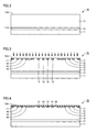
Fig. 2 is a schematic cross-sectional view illustrating the method for manufacturing a JBS. -
Fig. 3 is a schematic cross-sectional view illustrating the method for manufacturing a JBS. -
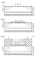
Fig. 4 is a schematic cross-sectional view illustrating the method for manufacturing a JBS. -
Fig. 5 is a schematic cross-sectional view illustrating the method for manufacturing a JBS. -
Fig. 6 is a schematic cross-sectional view illustrating the method for manufacturing a JBS. -
Fig. 7 is a schematic cross-sectional view illustrating the method for manufacturing a JBS. -
Fig. 8 is a schematic cross-sectional view illustrating the method for manufacturing a JBS. -
Fig. 9 is a schematic cross-sectional view illustrating a method for manufacturing a JBS according to a second embodiment. -
Fig. 10 is a schematic cross-sectional view illustrating the method for manufacturing a JBS according to the second embodiment. -
Fig. 11 is a schematic cross-sectional view illustrating the method for manufacturing a JBS according to the second embodiment. -
Fig. 12 illustrates the effect of heating temperature on average variation in film thickness of an oxide film. - Embodiments of the present invention will be described below with reference to the drawings. The same reference numerals are used to identify the same or corresponding features in the following drawings, and descriptions thereof will not be repeated.
- Referring to
Figs. 1 to 8 , first, a method for manufacturing a semiconductor device according to a first embodiment which is one embodiment of the present invention is described. Referring toFig. 1 , first, as a step (S10), a substrate preparation step is performed. In this step (S10), steps (S11) and (S 12) to be described below are performed to prepare asubstrate 10 made of silicon carbide. - First, as a step (S11), a base substrate preparation step is performed. In this step (S11), referring to
Fig. 2 , an ingot made of 4H-SiC (not shown) is cut into a slice, for example, to prepare abase substrate 11 made of silicon carbide and having an n conductivity type. - Next, as a step (S12), an epitaxial growth layer formation step is performed. In this step (S12), referring to
Fig. 2 , first, an electricfield stop layer 12 having an n conductivity type is formed by epitaxial growth on amain surface 11A ofbase substrate 11. Then, asemiconductor layer 13 having an n conductivity type is similarly formed by epitaxial growth on a main surface of electricfield stop layer 12 opposite tobase substrate 11. As such,substrate 10 having amain surface 10A and formed ofbase substrate 11, electricfield stop layer 12 andsemiconductor layer 13 is prepared. - Next, as a step (S20), an ion implantation step is performed. In this step (S20), referring to
Fig. 3 , first, Al (aluminum) ions are implanted intosemiconductor layer 13 as indicated with arrows in the figure, for example, to formp regions 15 having a p conductivity type. Then, Al ions are implanted into an area ofsemiconductor layer 13 which is closer to the outer edge thanp regions 15, for example, to formguard ring regions 16 having a p conductivity type. Then, P (phosphorus) ions are implanted into an area ofsemiconductor layer 13 which is closer to the outer edge thanguard ring regions 16, for example, to form afield stop region 17 having an n conductivity type. As such,p regions 15 andguard ring regions 16 as p type (second conductivity type) regions, andfield stop region 17 as an n type (first conductivity type) region are formed in a region includingmain surface 10A ofsubstrate 10. Put another way,p regions 15,guard ring regions 16 surroundingp regions 15, andfield stop region 17 surroundingp regions 15 andguard ring regions 16 are formed in the region includingmain surface 10A ofsubstrate 10. A region insemiconductor layer 13 in which neither ofp regions 15,guard ring regions 16 andfield stop region 17 is formed is adrift region 14, which forms an n type region together withfield stop region 17. In this step (S20), the ion implantations can be performed after a mask made of SiO2 (silicon dioxide) is formed onmain surface 10A ofsubstrate 10, for example, to form the impurity regions in desired positions insemiconductor layer 13, as shown inFig. 3 . - Next, as a step (S30), an activation annealing step is performed. In this step (S30),
substrate 10 is heated at a temperature of 1700°C for 30 minutes, for example, to activate the impurities introduced in the step (S20). As such, desired carriers are generated in the regions where the impurities have been introduced. - Next, as a step (S40), an oxide film formation step is performed. In this step (S40), referring to
Fig. 4 , anoxide film 20 made of SiO2 (silicon dioxide) is formed, for example, to covermain surface 10A ofsubstrate 10. Specifically,substrate 10 is heated at a temperature of 1250°C or more in an oxygen-containing atmosphere, to formoxide film 20 onmain surface 10A acrossdrift region 14 andfield stop region 17 as n type regions, andp regions 15 andguard ring regions 16 as p type regions. - Next, as a step (S50), a nitriding process step is performed. In this step (S50),
substrate 10 is heated in an atmosphere containing a gas including nitrogen atoms such as NO (nitric oxide), NO2 (nitrogen dioxide) or N2O (nitrous oxide), for example, to introduce the nitrogen atoms into a region including an interface betweenoxide film 20 and the silicon carbide that formssubstrate 10. Although this step (S50) is not an essential step of the method for manufacturing a semiconductor device of the present invention, if this step is performed, an interface state of the region including the interface betweenoxide film 20 and the silicon carbide that formssubstrate 10 can be reduced, to further improve breakdown voltage characteristics of aJBS 1. After the introduction of nitrogen atoms is completed, SiO2 (silicon dioxide) may further be deposited onoxide film 20 by CVD (Chemical Vapor Deposition), for example. Although this is not an essential step of the method for manufacturing a semiconductor device of the present invention, either, if this step is performed,oxide film 20 having a greater thickness can be formed. - Next, as a step (S60), an ohmic electrode formation step is performed. In this step (S60), referring to
Fig. 5 , first, a metallic film made of Ni (not shown) is formed by sputtering, for example, on amain surface 11B ofbase substrate 11 opposite tomain surface 11A. Then, the metallic film is heated at 1000°C, for example, to silicidize at least a part of the metallic film. As such, anohmic electrode 30 electrically connected tobase substrate 11 is formed. - Next, as a step (S70), a pad electrode formation step is performed. In this step (S70), referring to
Fig. 5 , apad electrode 40 made of a conductor such as NiAu and TiAu is formed onohmic electrode 30 by evaporation, for example. - Next, as a step (S80), an oxide film removal step is performed. In this step (S80),
oxide film 20 is removed to expose a part ofmain surface 10A ofsubstrate 10. Specifically,oxide film 20 is removed to expose a part ofdrift region 14 andp regions 15, as shown inFig. 6 , by dry etching such as RIE (Reactive Ion Etching) and wet etching with hydrofluoric acid, for example. If SiO2 (silicon dioxide) is further deposited onoxide film 20 that has been formed by thermal oxidation in the step (S40) as described above, in this step (S80),oxide film 20 formed by thermal oxidation and the SiO2 (silicon dioxide) deposited onoxide film 20 are removed to expose a part ofmain surface 10A ofsubstrate 10. - Next, as a step (S90), a Schottky electrode formation step is performed. In this step (S90), referring to
Fig. 7 , aSchottky electrode 50 is formed in contact withmain surface 10A ofsubstrate 10 that has been exposed by removingoxide film 20 in the step (S80) and withoxide film 20. Specifically, first, a metallic film made of Ti or TiAl (not shown) is formed onmain surface 10A andoxide film 20 by sputtering, for example. Then, the metallic film is heated at 500°C, for example, to silicidize at least a part of the metallic film, to formSchottky electrode 50 having thickness of 0.1 µm or more in contact withmain surface 10A, across one ofoxide films 20 and theother oxide film 20 with the contact portion interposed therebetween. - In this step (S90),
Schottky electrode 50 including at least one metal selected from the group consisting of Ti, W, Mo, Ni, Ta, Al and Au may be formed, orSchottky electrode 50 made of one metal selected from the group of metals above may be formed. Alternatively,Schottky electrode 50 made of an alloy of two or more metals selected from the group of metals above such as TiW or TiTa may be formed. Alternatively,Schottky electrode 50 having a metallic film made of one metal selected from the group of metals above and a metallic film made of another metal laminated one above the other may be formed. Still alternatively,Schottky electrode 50 made of nitride of one metal selected from the group of metals above such as TiN may be formed. As such, various types of materials capable of making Schottky contact withsubstrate 10 can be employed as a material forSchottky electrode 50. - Next, as a step (S100), a wire formation step is performed. In this step (S100), referring to
Fig. 8 , awire 60 made of a conductor such as Al is formed to surroundSchottky electrode 50 by evaporation, for example. - Next, as a step (S110), a passivation film formation step is performed. In this step (S110), referring to
Fig. 8 , apassivation film 70 made of SiO2 (silicon dioxide) is formed onoxide film 20 andwire 60 by CVD, for example. By performing the steps (S10) to (S110),JBS 1 is manufactured, and the method for manufacturing a semiconductor device according to this embodiment is completed. - As described above, in the method for manufacturing a semiconductor device according to this embodiment,
substrate 10 is heated at a temperature of 1250°C or more in the step (S40). Thus, the rate of formation ofoxide film 20 can be less dependent on the conductivity type, to formoxide film 20 with suppressed variation in film thickness. Accordingly, the surface roughness ofmain surface 10A ofsubstrate 10 exposed by removingoxide film 20 can be reduced, to obtain a satisfactory contact state betweensubstrate 10 andSchottky electrode 50 formed onmain surface 10A ofsubstrate 10. According to the method for manufacturing a semiconductor device of this embodiment, therefore, by obtaining the satisfactory contact state betweensubstrate 10 andSchottky electrode 50,JBS 1 with improved breakdown voltage characteristics can be manufactured. - Furthermore, in the method for manufacturing a semiconductor device according to this embodiment,
oxide film 20 is removed to expose a part ofmain surface 10A ofsubstrate 10, andSchottky electrode 50 is formed in contact withmain surface 10 that has been exposed by removingoxide film 20, and with remainingoxide film 20. Namely, remainingoxide film 20 can function as an electric field relaxation FP (Field Plate) to avoid electric field concentration at opposing ends ofSchottky electrode 50, thereby further improving the breakdown voltage characteristics ofJBS 1. Moreover, in the method for manufacturing a semiconductor device according to this embodiment,oxide film 20 is formed byheating substrate 10 at 1250°C or more as described above. As such, the roughness of the interface betweensubstrate 10 andoxide film 20 can be reduced, to further improve the function ofoxide film 20 as an electric field relaxation FP. If SiO2 (silicon dioxide) is further deposited onoxide film 20 that has been formed by thermal oxidation in the step (S40), and ifoxide film 20 formed by thermal oxidation and the SiO2 (silicon dioxide) deposited onoxide film 20 are removed in the step (S80), as described above,oxide film 20 having a greater thickness can be left, to further improve the function ofoxide film 20 as an electric field relaxation FP. - In the method for manufacturing a semiconductor device according to this embodiment, in the step (S40),
oxide film 20 having thickness of 0.1 µm or more may be formed. It is preferable to set the thickness ofoxide film 20 within such a practically suitable range, namely, within a range required to avoid breakdown ofoxide film 20. - Next, a method for manufacturing a semiconductor device according to a second embodiment which is another embodiment of the present invention will be described. The method for manufacturing a semiconductor device according to this embodiment is basically implemented similarly to that as discussed above with regard to the semiconductor device according to the first embodiment, and provides similar effects. The method for manufacturing a semiconductor device according to this embodiment, however, is different from the method for manufacturing a semiconductor device according to the first embodiment in that the oxide film is removed to expose the entire main surface of the substrate in the oxide film removal step.
- The method for manufacturing a semiconductor device according to this embodiment will be described. Referring to
Fig. 1 , first, the steps (S10) to (S70) are performed similarly to the first embodiment. The step (S50) is omitted in this embodiment. - Next, as the step (S80), the oxide film removal step is performed. In this step (S80), referring to
Fig. 9 ,oxide film 20 is removed to expose the entiremain surface 10A ofsubstrate 10. - Next, as the step (S90), the Schottky electrode formation step is performed. In this step (S90), referring to
Fig. 10 ,Schottky electrode 50 is formed in contact withmain surface 10A that has been exposed by removingoxide film 20 in the step (S80) similarly to the first embodiment. - Next, as the step (S100), the wire formation step is performed. In this step (S100), referring to
Fig. 11 ,wire 60 is formed to surroundSchottky electrode 50 similarly to the first embodiment. - Next, as the step (S110), the passivation film formation step is performed. In this step (S110), referring to
Fig. 11 ,passivation film 70 is formed onmain surface 10A ofsubstrate 10 andwire 60. By performing the steps (S10) to (S110), aJBS 2 is manufactured, and the method for manufacturing a semiconductor device according to this embodiment is completed. - As described above, in the methods for manufacturing a semiconductor device according to the first and second embodiments of the present invention,
substrate 10 is heated at a temperature of 1250°C or more in the step (S40). Thus, the rate of formation ofoxide film 20 can be less dependent on the conductivity type, to formoxide film 20 with suppressed variation in film thickness. Accordingly, the surface roughness ofmain surface 10A ofsubstrate 10 exposed by removingoxide film 20 can be reduced, to obtain a satisfactory contact state betweensubstrate 10 andSchottky electrode 50 formed onmain surface 10A ofsubstrate 10. According to the methods for manufacturing a semiconductor device of the first and second embodiments of the present invention, therefore, by obtaining the satisfactory contact state betweensubstrate 10 andSchottky electrode 50,JBS 1 with improved breakdown voltage characteristics can be manufactured. - In the methods for manufacturing a semiconductor device according to the first and second embodiments of the present invention, in the step (S40),
oxide film 20 may be formed onmain surface 10A ofsubstrate 10 byheating substrate 10 at a temperature of 1300°C or more. As such, variation in film thickness ofoxide film 20 can be suppressed more effectively. As a result, the contact betweensubstrate 10 andSchottky electrode 50 can be further enhanced, to further improve the breakdown voltage characteristics ofJBSs - Although the methods for manufacturing a semiconductor device according to the first and second embodiments of the present invention are only directed to the JBSs in which
p regions 15 are formed in the region includingmain surface 10A in contact withSchottky electrode 50, the method for manufacturing a semiconductor device of the present invention is not limited as such. Namely, the method for manufacturing a semiconductor device of the present invention can be employed in manufacturing a SBD in whichp regions 15 are not formed. As such, the roughness of the interface betweenoxide film 20 andsubstrate 10 can be reduced, to manufacture a SBD with improved characteristics ofoxide film 20 as an electric field relaxation FP. - Experiments were conducted to confirm the effect of the present invention on film thickness variation of an oxide film in a method for manufacturing a semiconductor device. Specifically, first, substrates each having an n type region with a (nitrogen) concentration of 8x1015 cm-3 formed to include one main surface were prepared. Next, Al ions were implanted in concentrations of 5×1017 cm-3, 5×1018 cm-3 and 5×1019 cm-3, respectively, into a region including the main surface of the substrates, to form a p type region. Next, the substrates were heated at 1200°C, 1250°C and 1300°C, respectively, to form an oxide film on the main surface across an n type region and the p type region. The thicknesses of the oxide films formed at the heating temperatures above were confirmed, respectively, to examine the effect of heating temperature on the average variation in film thickness of the oxide film due to the dependency of the rate of formation of the oxide film on the conductivity type.
- The experimental results are described with reference to
Fig. 12. Fig. 12 illustrates the effect of heating temperature on variation in film thickness of the oxide film. InFig. 12 , the abscissa represents the heating temperature (°C) of the substrate, the left ordinate represents the thickness (Å) of the oxide film, and the right ordinate represents average variation (%) in film thickness of the oxide film. The average variation as used herein refers to a standard deviation (σ) of the film thickness of the oxide film. - As is clear from
Fig. 12 , when the substrate was heated at a temperature of 1250°C or more, the average variation in film thickness of the oxide film was smaller than that when the substrate was heated at 1200°C. It was thus confirmed that the variation in film thickness of the formed oxide film could be suppressed by setting the heating temperature of the substrate when forming the oxide film to 1250°C or more, preferably to 1300°C or more, in the method for manufacturing a semiconductor device of the present invention. - It should be understood that the embodiments and examples disclosed herein are illustrative and non-restrictive in every respect. The scope of the present invention is defined by the terms of the claims, rather than the description above, and is intended to include any modifications within the scope and meaning equivalent to the terms of the claims.
- The method for manufacturing a semiconductor device of the present invention is applicable particularly advantageously to a method for manufacturing a semiconductor device required to achieve improved breakdown voltage characteristics.
- 1 JBS; 10 substrate; 11 base substrate; 10A, 11A, 11B main surface; 12 electric field stop layer; 13 semiconductor layer; 14 drift region; 15 p region; 16 guard ring region; 17 field stop region; 20 oxide film; 30 ohmic electrode; 40 pad electrode; 50 Schottky electrode; 60 wire; 70 passivation film.
Claims (7)
- A method for manufacturing a semiconductor device, comprising the steps of:preparing a substrate (10) made of silicon carbide and having a first conductivity type region (14, 17) formed to include one main surface (10A);forming a second conductivity type region (15, 16) in a region including said main surface (10A);forming an oxide film (20) on said main surface (10A) across said first conductivity type region (14, 17) and said second conductivity type region (15, 16), by heating said substrate (10) having said second conductivity type region (15, 16) formed therein at a temperature of 1250°C or more;removing said oxide film (20) to expose at least a part of said main surface (10A); andforming a Schottky electrode (50) in contact with said main surface (10A) that has been exposed by removing said oxide film (20).
- The method for manufacturing a semiconductor device according to claim 1, wherein
in said step of forming an oxide film (20), said oxide film (20) is formed on said main surface (10A) by heating said substrate (10) at a temperature of 1300°C or more. - The method for manufacturing a semiconductor device according to claim 1 or 2, wherein
in said step of removing said oxide film (20), said oxide film (20) is removed to expose a part of said main surface (10A), and
in said step of forming a Schottky electrode (50), said Schottky electrode (50) is formed in contact with said main surface (10A) that has been exposed by removing said oxide film (20) and with said oxide film (20). - The method for manufacturing a semiconductor device according to claim 3, further comprising the step of heating said substrate (10) having said oxide film (20) formed thereon in a nitrogen-containing atmosphere, before said step of removing said oxide film (20).
- The method for manufacturing a semiconductor device according to claim 3 or 4, wherein
in said step of forming an oxide film (20), said oxide film (20) having a thickness of 0.1 µm or more is formed. - The method for manufacturing a semiconductor device according to claim 1 or 2, wherein
in said step of removing said oxide film (20), said oxide film (20) is removed to expose the entire said main surface (10A). - The method for manufacturing a semiconductor device according to any one of claims 1 to 6, wherein
in said step of forming a Schottky electrode (50), said Schottky electrode (50) including at least one selected from the group consisting of Ti, W, Mo, Ni, Ta, Al and Au is formed.
Applications Claiming Priority (2)
| Application Number | Priority Date | Filing Date | Title |
|---|---|---|---|
| JP2011267604A JP2013120822A (en) | 2011-12-07 | 2011-12-07 | Semiconductor device manufacturing method |
| PCT/JP2012/077858 WO2013084620A1 (en) | 2011-12-07 | 2012-10-29 | Method for manufacturing semiconductor device |
Publications (3)
| Publication Number | Publication Date |
|---|---|
| EP2790225A1 true EP2790225A1 (en) | 2014-10-15 |
| EP2790225A4 EP2790225A4 (en) | 2015-07-15 |
| EP2790225B1 EP2790225B1 (en) | 2019-01-23 |
Family
ID=48572355
Family Applications (1)
| Application Number | Title | Priority Date | Filing Date |
|---|---|---|---|
| EP12854962.3A Not-in-force EP2790225B1 (en) | 2011-12-07 | 2012-10-29 | Method for manufacturing silicon carbide semiconductor device |
Country Status (5)
| Country | Link |
|---|---|
| US (1) | US8765523B2 (en) |
| EP (1) | EP2790225B1 (en) |
| JP (1) | JP2013120822A (en) |
| CN (1) | CN103918081A (en) |
| WO (1) | WO2013084620A1 (en) |
Families Citing this family (12)
| Publication number | Priority date | Publication date | Assignee | Title |
|---|---|---|---|---|
| JP2015032627A (en) * | 2013-07-31 | 2015-02-16 | 株式会社東芝 | Semiconductor device |
| JP6202944B2 (en) * | 2013-08-28 | 2017-09-27 | 三菱電機株式会社 | Silicon carbide semiconductor device and manufacturing method thereof |
| CN104269443B (en) * | 2014-09-28 | 2017-04-12 | 北京燕东微电子有限公司 | Constant current diode |
| JP2016081981A (en) * | 2014-10-14 | 2016-05-16 | 株式会社日立製作所 | Semiconductor device and manufacturing method of the same |
| DE102014118874B4 (en) * | 2014-12-17 | 2025-09-18 | Infineon Technologies Austria Ag | Semiconductor device and method for manufacturing a semiconductor device |
| JP2017017309A (en) * | 2015-04-14 | 2017-01-19 | ローム株式会社 | diode |
| JP6592950B2 (en) * | 2015-04-24 | 2019-10-23 | 富士電機株式会社 | Method for manufacturing silicon carbide semiconductor device |
| JP6439774B2 (en) * | 2016-11-21 | 2018-12-19 | トヨタ自動車株式会社 | Manufacturing method of semiconductor device |
| CN113517356B (en) * | 2021-05-21 | 2023-08-04 | 浙江芯科半导体有限公司 | 4H-SiC diode based on step-shaped P-type CBN and SiC mixed structure and preparation method thereof |
| CN114446784A (en) * | 2022-04-11 | 2022-05-06 | 深圳芯能半导体技术有限公司 | Silicon carbide junction barrier Schottky diode and preparation method thereof |
| CN114464532B (en) * | 2022-04-13 | 2022-07-12 | 深圳芯能半导体技术有限公司 | Method for manufacturing silicon carbide Schottky diode |
| CN114864704B (en) * | 2022-07-11 | 2022-09-27 | 成都功成半导体有限公司 | Silicon carbide JBS with terminal protection device and preparation method thereof |
Family Cites Families (16)
| Publication number | Priority date | Publication date | Assignee | Title |
|---|---|---|---|---|
| JP3439593B2 (en) | 1996-03-11 | 2003-08-25 | 新日本製鐵株式会社 | Method of manufacturing Schottky barrier diode made of SiC |
| WO2001022474A2 (en) * | 1999-09-22 | 2001-03-29 | Siced Electronics Development Gmbh & Co. Kg | Method for producing a semiconductor device consisting of silicon-carbide and comprising a schottky contact |
| JP2006253521A (en) * | 2005-03-14 | 2006-09-21 | Kansai Tlo Kk | Semiconductor diode device and manufacturing method thereof |
| US20100221917A1 (en) | 2006-01-30 | 2010-09-02 | Sumitomo Electric Industries, Ltd. | Method of manufacturing silicon carbide semiconductor device |
| JP4189415B2 (en) * | 2006-06-30 | 2008-12-03 | 株式会社東芝 | Semiconductor device |
| JP4314277B2 (en) * | 2007-01-11 | 2009-08-12 | 株式会社東芝 | SiC Schottky barrier semiconductor device |
| JP2009212366A (en) * | 2008-03-05 | 2009-09-17 | Oki Semiconductor Co Ltd | Method of manufacturing semiconductor device |
| JP5171363B2 (en) * | 2008-04-08 | 2013-03-27 | 三菱電機株式会社 | Manufacturing method of semiconductor device |
| JP5435922B2 (en) * | 2008-08-12 | 2014-03-05 | 新電元工業株式会社 | Manufacturing method of Schottky barrier diode |
| JP5408929B2 (en) * | 2008-08-21 | 2014-02-05 | 昭和電工株式会社 | Semiconductor device and manufacturing method of semiconductor device |
| JP5525940B2 (en) * | 2009-07-21 | 2014-06-18 | ローム株式会社 | Semiconductor device and manufacturing method of semiconductor device |
| JP5443908B2 (en) * | 2009-09-09 | 2014-03-19 | 株式会社東芝 | Manufacturing method of semiconductor device |
| JP5175872B2 (en) * | 2010-01-21 | 2013-04-03 | 株式会社東芝 | Semiconductor rectifier |
| JP5598015B2 (en) * | 2010-02-23 | 2014-10-01 | 株式会社デンソー | Silicon carbide semiconductor device having Schottky barrier diode and method for manufacturing the same |
| DE112010005626B4 (en) * | 2010-06-02 | 2024-02-15 | Hitachi Power Semiconductor Device, Ltd. | Semiconductor device |
| JP5269015B2 (en) * | 2010-09-08 | 2013-08-21 | 株式会社東芝 | Semiconductor device and manufacturing method of semiconductor device |
-
2011
- 2011-12-07 JP JP2011267604A patent/JP2013120822A/en active Pending
-
2012
- 2012-10-29 CN CN201280054480.9A patent/CN103918081A/en active Pending
- 2012-10-29 WO PCT/JP2012/077858 patent/WO2013084620A1/en not_active Ceased
- 2012-10-29 EP EP12854962.3A patent/EP2790225B1/en not_active Not-in-force
- 2012-11-06 US US13/670,119 patent/US8765523B2/en not_active Expired - Fee Related
Also Published As
| Publication number | Publication date |
|---|---|
| JP2013120822A (en) | 2013-06-17 |
| US8765523B2 (en) | 2014-07-01 |
| EP2790225B1 (en) | 2019-01-23 |
| US20130149850A1 (en) | 2013-06-13 |
| CN103918081A (en) | 2014-07-09 |
| WO2013084620A1 (en) | 2013-06-13 |
| EP2790225A4 (en) | 2015-07-15 |
Similar Documents
| Publication | Publication Date | Title |
|---|---|---|
| EP2790225B1 (en) | Method for manufacturing silicon carbide semiconductor device | |
| CN104272442B (en) | The manufacture method of semiconductor devices | |
| US9240451B2 (en) | Silicon carbide semiconductor device | |
| CN103548119B (en) | SiC semiconductor device and process for producing same | |
| EP2388803B1 (en) | Silicon carbide semiconductor device and method for producing silicon carbide semiconductor device | |
| EP2698808B1 (en) | Method for manufacturing a silicon carbide semiconductor device | |
| US10600921B2 (en) | Silicon carbide semiconductor device and method of manufacturing silicon carbide semiconductor device | |
| EP2966676B1 (en) | Silicon-carbide semiconductor device and manufacturing method therefor | |
| JP2011044688A (en) | Semiconductor device and manufacturing method thereof | |
| US9768260B2 (en) | Fabrication method of silicon carbide semiconductor apparatus and silicon carbide semiconductor apparatus fabricated thereby | |
| CN111801804B (en) | Trench MOS type Schottky diode and manufacturing method thereof | |
| EP2966674A1 (en) | Method for manufacturing silicon-carbide semiconductor device | |
| EP2685488A1 (en) | Production method for semiconductor device | |
| US9653297B2 (en) | Method of manufacturing silicon carbide semiconductor device by forming metal-free protection film | |
| EP2096669A1 (en) | Method for manufacturing silicon carbide semiconductor device | |
| JP2016178336A (en) | Semiconductor device manufacturing method | |
| CA2787837A1 (en) | Method of manufacturing semiconductor device | |
| JP6152701B2 (en) | Silicon carbide semiconductor device manufacturing method and silicon carbide semiconductor device | |
| CN104285299A (en) | Silicon carbide semiconductor device |
Legal Events
| Date | Code | Title | Description |
|---|---|---|---|
| PUAI | Public reference made under article 153(3) epc to a published international application that has entered the european phase |
Free format text: ORIGINAL CODE: 0009012 |
|
| 17P | Request for examination filed |
Effective date: 20140326 |
|
| AK | Designated contracting states |
Kind code of ref document: A1 Designated state(s): AL AT BE BG CH CY CZ DE DK EE ES FI FR GB GR HR HU IE IS IT LI LT LU LV MC MK MT NL NO PL PT RO RS SE SI SK SM TR |
|
| DAX | Request for extension of the european patent (deleted) | ||
| RA4 | Supplementary search report drawn up and despatched (corrected) |
Effective date: 20150617 |
|
| RIC1 | Information provided on ipc code assigned before grant |
Ipc: H01L 21/04 20060101ALI20150611BHEP Ipc: H01L 29/47 20060101ALN20150611BHEP Ipc: H01L 29/06 20060101ALN20150611BHEP Ipc: H01L 21/329 20060101AFI20150611BHEP Ipc: H01L 29/872 20060101ALI20150611BHEP Ipc: H01L 29/24 20060101ALI20150611BHEP |
|
| STAA | Information on the status of an ep patent application or granted ep patent |
Free format text: STATUS: EXAMINATION IS IN PROGRESS |
|
| 17Q | First examination report despatched |
Effective date: 20180528 |
|
| RIC1 | Information provided on ipc code assigned before grant |
Ipc: H01L 21/329 20060101AFI20180615BHEP Ipc: H01L 29/16 20060101ALI20180615BHEP Ipc: H01L 29/47 20060101ALN20180615BHEP Ipc: H01L 29/872 20060101ALI20180615BHEP Ipc: H01L 29/06 20060101ALN20180615BHEP Ipc: H01L 21/04 20060101ALI20180615BHEP |
|
| RIC1 | Information provided on ipc code assigned before grant |
Ipc: H01L 29/47 20060101ALN20180629BHEP Ipc: H01L 21/04 20060101ALI20180629BHEP Ipc: H01L 21/329 20060101AFI20180629BHEP Ipc: H01L 29/16 20060101ALI20180629BHEP Ipc: H01L 29/872 20060101ALI20180629BHEP Ipc: H01L 29/06 20060101ALN20180629BHEP |
|
| REG | Reference to a national code |
Ref country code: DE Ref legal event code: R079 Ref document number: 602012056336 Country of ref document: DE Free format text: PREVIOUS MAIN CLASS: H01L0029470000 Ipc: H01L0021329000 |
|
| GRAP | Despatch of communication of intention to grant a patent |
Free format text: ORIGINAL CODE: EPIDOSNIGR1 |
|
| STAA | Information on the status of an ep patent application or granted ep patent |
Free format text: STATUS: GRANT OF PATENT IS INTENDED |
|
| RIC1 | Information provided on ipc code assigned before grant |
Ipc: H01L 29/16 20060101ALI20180814BHEP Ipc: H01L 21/04 20060101ALI20180814BHEP Ipc: H01L 21/329 20060101AFI20180814BHEP Ipc: H01L 29/47 20060101ALN20180814BHEP Ipc: H01L 29/06 20060101ALN20180814BHEP Ipc: H01L 29/872 20060101ALI20180814BHEP |
|
| INTG | Intention to grant announced |
Effective date: 20180827 |
|
| GRAS | Grant fee paid |
Free format text: ORIGINAL CODE: EPIDOSNIGR3 |
|
| GRAA | (expected) grant |
Free format text: ORIGINAL CODE: 0009210 |
|
| STAA | Information on the status of an ep patent application or granted ep patent |
Free format text: STATUS: THE PATENT HAS BEEN GRANTED |
|
| AK | Designated contracting states |
Kind code of ref document: B1 Designated state(s): AL AT BE BG CH CY CZ DE DK EE ES FI FR GB GR HR HU IE IS IT LI LT LU LV MC MK MT NL NO PL PT RO RS SE SI SK SM TR |
|
| REG | Reference to a national code |
Ref country code: GB Ref legal event code: FG4D |
|
| REG | Reference to a national code |
Ref country code: CH Ref legal event code: EP |
|
| REG | Reference to a national code |
Ref country code: AT Ref legal event code: REF Ref document number: 1092130 Country of ref document: AT Kind code of ref document: T Effective date: 20190215 |
|
| REG | Reference to a national code |
Ref country code: IE Ref legal event code: FG4D |
|
| REG | Reference to a national code |
Ref country code: DE Ref legal event code: R096 Ref document number: 602012056336 Country of ref document: DE |
|
| REG | Reference to a national code |
Ref country code: NL Ref legal event code: MP Effective date: 20190123 |
|
| PG25 | Lapsed in a contracting state [announced via postgrant information from national office to epo] |
Ref country code: NL Free format text: LAPSE BECAUSE OF FAILURE TO SUBMIT A TRANSLATION OF THE DESCRIPTION OR TO PAY THE FEE WITHIN THE PRESCRIBED TIME-LIMIT Effective date: 20190123 |
|
| PG25 | Lapsed in a contracting state [announced via postgrant information from national office to epo] |
Ref country code: ES Free format text: LAPSE BECAUSE OF FAILURE TO SUBMIT A TRANSLATION OF THE DESCRIPTION OR TO PAY THE FEE WITHIN THE PRESCRIBED TIME-LIMIT Effective date: 20190123 Ref country code: FI Free format text: LAPSE BECAUSE OF FAILURE TO SUBMIT A TRANSLATION OF THE DESCRIPTION OR TO PAY THE FEE WITHIN THE PRESCRIBED TIME-LIMIT Effective date: 20190123 Ref country code: NO Free format text: LAPSE BECAUSE OF FAILURE TO SUBMIT A TRANSLATION OF THE DESCRIPTION OR TO PAY THE FEE WITHIN THE PRESCRIBED TIME-LIMIT Effective date: 20190423 Ref country code: PT Free format text: LAPSE BECAUSE OF FAILURE TO SUBMIT A TRANSLATION OF THE DESCRIPTION OR TO PAY THE FEE WITHIN THE PRESCRIBED TIME-LIMIT Effective date: 20190523 Ref country code: SE Free format text: LAPSE BECAUSE OF FAILURE TO SUBMIT A TRANSLATION OF THE DESCRIPTION OR TO PAY THE FEE WITHIN THE PRESCRIBED TIME-LIMIT Effective date: 20190123 Ref country code: PL Free format text: LAPSE BECAUSE OF FAILURE TO SUBMIT A TRANSLATION OF THE DESCRIPTION OR TO PAY THE FEE WITHIN THE PRESCRIBED TIME-LIMIT Effective date: 20190123 Ref country code: LT Free format text: LAPSE BECAUSE OF FAILURE TO SUBMIT A TRANSLATION OF THE DESCRIPTION OR TO PAY THE FEE WITHIN THE PRESCRIBED TIME-LIMIT Effective date: 20190123 |
|
| REG | Reference to a national code |
Ref country code: AT Ref legal event code: MK05 Ref document number: 1092130 Country of ref document: AT Kind code of ref document: T Effective date: 20190123 |
|
| PG25 | Lapsed in a contracting state [announced via postgrant information from national office to epo] |
Ref country code: HR Free format text: LAPSE BECAUSE OF FAILURE TO SUBMIT A TRANSLATION OF THE DESCRIPTION OR TO PAY THE FEE WITHIN THE PRESCRIBED TIME-LIMIT Effective date: 20190123 Ref country code: RS Free format text: LAPSE BECAUSE OF FAILURE TO SUBMIT A TRANSLATION OF THE DESCRIPTION OR TO PAY THE FEE WITHIN THE PRESCRIBED TIME-LIMIT Effective date: 20190123 Ref country code: BG Free format text: LAPSE BECAUSE OF FAILURE TO SUBMIT A TRANSLATION OF THE DESCRIPTION OR TO PAY THE FEE WITHIN THE PRESCRIBED TIME-LIMIT Effective date: 20190423 Ref country code: IS Free format text: LAPSE BECAUSE OF FAILURE TO SUBMIT A TRANSLATION OF THE DESCRIPTION OR TO PAY THE FEE WITHIN THE PRESCRIBED TIME-LIMIT Effective date: 20190523 Ref country code: GR Free format text: LAPSE BECAUSE OF FAILURE TO SUBMIT A TRANSLATION OF THE DESCRIPTION OR TO PAY THE FEE WITHIN THE PRESCRIBED TIME-LIMIT Effective date: 20190424 Ref country code: LV Free format text: LAPSE BECAUSE OF FAILURE TO SUBMIT A TRANSLATION OF THE DESCRIPTION OR TO PAY THE FEE WITHIN THE PRESCRIBED TIME-LIMIT Effective date: 20190123 |
|
| REG | Reference to a national code |
Ref country code: DE Ref legal event code: R097 Ref document number: 602012056336 Country of ref document: DE |
|
| PG25 | Lapsed in a contracting state [announced via postgrant information from national office to epo] |
Ref country code: EE Free format text: LAPSE BECAUSE OF FAILURE TO SUBMIT A TRANSLATION OF THE DESCRIPTION OR TO PAY THE FEE WITHIN THE PRESCRIBED TIME-LIMIT Effective date: 20190123 Ref country code: SK Free format text: LAPSE BECAUSE OF FAILURE TO SUBMIT A TRANSLATION OF THE DESCRIPTION OR TO PAY THE FEE WITHIN THE PRESCRIBED TIME-LIMIT Effective date: 20190123 Ref country code: DK Free format text: LAPSE BECAUSE OF FAILURE TO SUBMIT A TRANSLATION OF THE DESCRIPTION OR TO PAY THE FEE WITHIN THE PRESCRIBED TIME-LIMIT Effective date: 20190123 Ref country code: IT Free format text: LAPSE BECAUSE OF FAILURE TO SUBMIT A TRANSLATION OF THE DESCRIPTION OR TO PAY THE FEE WITHIN THE PRESCRIBED TIME-LIMIT Effective date: 20190123 Ref country code: AL Free format text: LAPSE BECAUSE OF FAILURE TO SUBMIT A TRANSLATION OF THE DESCRIPTION OR TO PAY THE FEE WITHIN THE PRESCRIBED TIME-LIMIT Effective date: 20190123 Ref country code: RO Free format text: LAPSE BECAUSE OF FAILURE TO SUBMIT A TRANSLATION OF THE DESCRIPTION OR TO PAY THE FEE WITHIN THE PRESCRIBED TIME-LIMIT Effective date: 20190123 Ref country code: CZ Free format text: LAPSE BECAUSE OF FAILURE TO SUBMIT A TRANSLATION OF THE DESCRIPTION OR TO PAY THE FEE WITHIN THE PRESCRIBED TIME-LIMIT Effective date: 20190123 |
|
| PG25 | Lapsed in a contracting state [announced via postgrant information from national office to epo] |
Ref country code: SM Free format text: LAPSE BECAUSE OF FAILURE TO SUBMIT A TRANSLATION OF THE DESCRIPTION OR TO PAY THE FEE WITHIN THE PRESCRIBED TIME-LIMIT Effective date: 20190123 |
|
| PLBE | No opposition filed within time limit |
Free format text: ORIGINAL CODE: 0009261 |
|
| STAA | Information on the status of an ep patent application or granted ep patent |
Free format text: STATUS: NO OPPOSITION FILED WITHIN TIME LIMIT |
|
| PG25 | Lapsed in a contracting state [announced via postgrant information from national office to epo] |
Ref country code: AT Free format text: LAPSE BECAUSE OF FAILURE TO SUBMIT A TRANSLATION OF THE DESCRIPTION OR TO PAY THE FEE WITHIN THE PRESCRIBED TIME-LIMIT Effective date: 20190123 |
|
| 26N | No opposition filed |
Effective date: 20191024 |
|
| PG25 | Lapsed in a contracting state [announced via postgrant information from national office to epo] |
Ref country code: SI Free format text: LAPSE BECAUSE OF FAILURE TO SUBMIT A TRANSLATION OF THE DESCRIPTION OR TO PAY THE FEE WITHIN THE PRESCRIBED TIME-LIMIT Effective date: 20190123 |
|
| PG25 | Lapsed in a contracting state [announced via postgrant information from national office to epo] |
Ref country code: TR Free format text: LAPSE BECAUSE OF FAILURE TO SUBMIT A TRANSLATION OF THE DESCRIPTION OR TO PAY THE FEE WITHIN THE PRESCRIBED TIME-LIMIT Effective date: 20190123 |
|
| PG25 | Lapsed in a contracting state [announced via postgrant information from national office to epo] |
Ref country code: MC Free format text: LAPSE BECAUSE OF FAILURE TO SUBMIT A TRANSLATION OF THE DESCRIPTION OR TO PAY THE FEE WITHIN THE PRESCRIBED TIME-LIMIT Effective date: 20190123 |
|
| REG | Reference to a national code |
Ref country code: CH Ref legal event code: PL |
|
| PG25 | Lapsed in a contracting state [announced via postgrant information from national office to epo] |
Ref country code: LU Free format text: LAPSE BECAUSE OF NON-PAYMENT OF DUE FEES Effective date: 20191029 Ref country code: CH Free format text: LAPSE BECAUSE OF NON-PAYMENT OF DUE FEES Effective date: 20191031 Ref country code: LI Free format text: LAPSE BECAUSE OF NON-PAYMENT OF DUE FEES Effective date: 20191031 |
|
| REG | Reference to a national code |
Ref country code: BE Ref legal event code: MM Effective date: 20191031 |
|
| PG25 | Lapsed in a contracting state [announced via postgrant information from national office to epo] |
Ref country code: BE Free format text: LAPSE BECAUSE OF NON-PAYMENT OF DUE FEES Effective date: 20191031 |
|
| GBPC | Gb: european patent ceased through non-payment of renewal fee |
Effective date: 20191029 |
|
| PG25 | Lapsed in a contracting state [announced via postgrant information from national office to epo] |
Ref country code: FR Free format text: LAPSE BECAUSE OF NON-PAYMENT OF DUE FEES Effective date: 20191031 Ref country code: IE Free format text: LAPSE BECAUSE OF NON-PAYMENT OF DUE FEES Effective date: 20191029 Ref country code: GB Free format text: LAPSE BECAUSE OF NON-PAYMENT OF DUE FEES Effective date: 20191029 |
|
| PG25 | Lapsed in a contracting state [announced via postgrant information from national office to epo] |
Ref country code: CY Free format text: LAPSE BECAUSE OF FAILURE TO SUBMIT A TRANSLATION OF THE DESCRIPTION OR TO PAY THE FEE WITHIN THE PRESCRIBED TIME-LIMIT Effective date: 20190123 |
|
| PG25 | Lapsed in a contracting state [announced via postgrant information from national office to epo] |
Ref country code: HU Free format text: LAPSE BECAUSE OF FAILURE TO SUBMIT A TRANSLATION OF THE DESCRIPTION OR TO PAY THE FEE WITHIN THE PRESCRIBED TIME-LIMIT; INVALID AB INITIO Effective date: 20121029 Ref country code: MT Free format text: LAPSE BECAUSE OF FAILURE TO SUBMIT A TRANSLATION OF THE DESCRIPTION OR TO PAY THE FEE WITHIN THE PRESCRIBED TIME-LIMIT Effective date: 20190123 |
|
| PG25 | Lapsed in a contracting state [announced via postgrant information from national office to epo] |
Ref country code: MK Free format text: LAPSE BECAUSE OF FAILURE TO SUBMIT A TRANSLATION OF THE DESCRIPTION OR TO PAY THE FEE WITHIN THE PRESCRIBED TIME-LIMIT Effective date: 20190123 |
|
| P01 | Opt-out of the competence of the unified patent court (upc) registered |
Effective date: 20230515 |
|
| PGFP | Annual fee paid to national office [announced via postgrant information from national office to epo] |
Ref country code: DE Payment date: 20230906 Year of fee payment: 12 |
|
| REG | Reference to a national code |
Ref country code: DE Ref legal event code: R079 Ref document number: 602012056336 Country of ref document: DE Free format text: PREVIOUS MAIN CLASS: H01L0021329000 Ipc: H10D0008010000 |
|
| REG | Reference to a national code |
Ref country code: DE Ref legal event code: R119 Ref document number: 602012056336 Country of ref document: DE |
|
| PG25 | Lapsed in a contracting state [announced via postgrant information from national office to epo] |
Ref country code: DE Free format text: LAPSE BECAUSE OF NON-PAYMENT OF DUE FEES Effective date: 20250501 |