EP2789016B1 - Method for the industrial production of photovoltaic concentrator modules - Google Patents
Method for the industrial production of photovoltaic concentrator modules Download PDFInfo
- Publication number
- EP2789016B1 EP2789016B1 EP12812520.0A EP12812520A EP2789016B1 EP 2789016 B1 EP2789016 B1 EP 2789016B1 EP 12812520 A EP12812520 A EP 12812520A EP 2789016 B1 EP2789016 B1 EP 2789016B1
- Authority
- EP
- European Patent Office
- Prior art keywords
- disc
- module frame
- acrylic
- lens
- sensor carrier
- Prior art date
- Legal status (The legal status is an assumption and is not a legal conclusion. Google has not performed a legal analysis and makes no representation as to the accuracy of the status listed.)
- Not-in-force
Links
Images



Classifications
-
- H—ELECTRICITY
- H10—SEMICONDUCTOR DEVICES; ELECTRIC SOLID-STATE DEVICES NOT OTHERWISE PROVIDED FOR
- H10P—GENERIC PROCESSES OR APPARATUS FOR THE MANUFACTURE OR TREATMENT OF DEVICES COVERED BY CLASS H10
- H10P72/00—Handling or holding of wafers, substrates or devices during manufacture or treatment thereof
- H10P72/04—Apparatus for manufacture or treatment
- H10P72/0448—Apparatus for applying a liquid, a resin, an ink or the like
-
- H—ELECTRICITY
- H10—SEMICONDUCTOR DEVICES; ELECTRIC SOLID-STATE DEVICES NOT OTHERWISE PROVIDED FOR
- H10F—INORGANIC SEMICONDUCTOR DEVICES SENSITIVE TO INFRARED RADIATION, LIGHT, ELECTROMAGNETIC RADIATION OF SHORTER WAVELENGTH OR CORPUSCULAR RADIATION
- H10F77/00—Constructional details of devices covered by this subclass
- H10F77/60—Arrangements for cooling, heating, ventilating or compensating for temperature fluctuations
- H10F77/63—Arrangements for cooling directly associated or integrated with photovoltaic cells, e.g. heat sinks directly associated with the photovoltaic cells or integrated Peltier elements for active cooling
-
- H—ELECTRICITY
- H10—SEMICONDUCTOR DEVICES; ELECTRIC SOLID-STATE DEVICES NOT OTHERWISE PROVIDED FOR
- H10F—INORGANIC SEMICONDUCTOR DEVICES SENSITIVE TO INFRARED RADIATION, LIGHT, ELECTROMAGNETIC RADIATION OF SHORTER WAVELENGTH OR CORPUSCULAR RADIATION
- H10F19/00—Integrated devices, or assemblies of multiple devices, comprising at least one photovoltaic cell covered by group H10F10/00, e.g. photovoltaic modules
- H10F19/70—Integrated devices, or assemblies of multiple devices, comprising at least one photovoltaic cell covered by group H10F10/00, e.g. photovoltaic modules comprising bypass diodes
-
- H—ELECTRICITY
- H10—SEMICONDUCTOR DEVICES; ELECTRIC SOLID-STATE DEVICES NOT OTHERWISE PROVIDED FOR
- H10F—INORGANIC SEMICONDUCTOR DEVICES SENSITIVE TO INFRARED RADIATION, LIGHT, ELECTROMAGNETIC RADIATION OF SHORTER WAVELENGTH OR CORPUSCULAR RADIATION
- H10F19/00—Integrated devices, or assemblies of multiple devices, comprising at least one photovoltaic cell covered by group H10F10/00, e.g. photovoltaic modules
- H10F19/80—Encapsulations or containers for integrated devices, or assemblies of multiple devices, having photovoltaic cells
-
- H—ELECTRICITY
- H10—SEMICONDUCTOR DEVICES; ELECTRIC SOLID-STATE DEVICES NOT OTHERWISE PROVIDED FOR
- H10F—INORGANIC SEMICONDUCTOR DEVICES SENSITIVE TO INFRARED RADIATION, LIGHT, ELECTROMAGNETIC RADIATION OF SHORTER WAVELENGTH OR CORPUSCULAR RADIATION
- H10F19/00—Integrated devices, or assemblies of multiple devices, comprising at least one photovoltaic cell covered by group H10F10/00, e.g. photovoltaic modules
- H10F19/90—Structures for connecting between photovoltaic cells, e.g. interconnections or insulating spacers
- H10F19/902—Structures for connecting between photovoltaic cells, e.g. interconnections or insulating spacers for series or parallel connection of photovoltaic cells
-
- H—ELECTRICITY
- H10—SEMICONDUCTOR DEVICES; ELECTRIC SOLID-STATE DEVICES NOT OTHERWISE PROVIDED FOR
- H10F—INORGANIC SEMICONDUCTOR DEVICES SENSITIVE TO INFRARED RADIATION, LIGHT, ELECTROMAGNETIC RADIATION OF SHORTER WAVELENGTH OR CORPUSCULAR RADIATION
- H10F71/00—Manufacture or treatment of devices covered by this subclass
- H10F71/137—Batch treatment of the devices
-
- H—ELECTRICITY
- H10—SEMICONDUCTOR DEVICES; ELECTRIC SOLID-STATE DEVICES NOT OTHERWISE PROVIDED FOR
- H10F—INORGANIC SEMICONDUCTOR DEVICES SENSITIVE TO INFRARED RADIATION, LIGHT, ELECTROMAGNETIC RADIATION OF SHORTER WAVELENGTH OR CORPUSCULAR RADIATION
- H10F71/00—Manufacture or treatment of devices covered by this subclass
- H10F71/137—Batch treatment of the devices
- H10F71/1375—Apparatus for automatic interconnection of photovoltaic cells in a module
-
- H—ELECTRICITY
- H10—SEMICONDUCTOR DEVICES; ELECTRIC SOLID-STATE DEVICES NOT OTHERWISE PROVIDED FOR
- H10F—INORGANIC SEMICONDUCTOR DEVICES SENSITIVE TO INFRARED RADIATION, LIGHT, ELECTROMAGNETIC RADIATION OF SHORTER WAVELENGTH OR CORPUSCULAR RADIATION
- H10F77/00—Constructional details of devices covered by this subclass
- H10F77/40—Optical elements or arrangements
- H10F77/42—Optical elements or arrangements directly associated or integrated with photovoltaic cells, e.g. light-reflecting means or light-concentrating means
- H10F77/484—Refractive light-concentrating means, e.g. lenses
-
- H—ELECTRICITY
- H10—SEMICONDUCTOR DEVICES; ELECTRIC SOLID-STATE DEVICES NOT OTHERWISE PROVIDED FOR
- H10P—GENERIC PROCESSES OR APPARATUS FOR THE MANUFACTURE OR TREATMENT OF DEVICES COVERED BY CLASS H10
- H10P72/00—Handling or holding of wafers, substrates or devices during manufacture or treatment thereof
- H10P72/30—Handling or holding of wafers, substrates or devices during manufacture or treatment thereof for conveying, e.g. between different workstations
- H10P72/32—Handling or holding of wafers, substrates or devices during manufacture or treatment thereof for conveying, e.g. between different workstations between different workstations
- H10P72/3202—Mechanical details, e.g. rollers or belts
-
- H—ELECTRICITY
- H10—SEMICONDUCTOR DEVICES; ELECTRIC SOLID-STATE DEVICES NOT OTHERWISE PROVIDED FOR
- H10P—GENERIC PROCESSES OR APPARATUS FOR THE MANUFACTURE OR TREATMENT OF DEVICES COVERED BY CLASS H10
- H10P72/00—Handling or holding of wafers, substrates or devices during manufacture or treatment thereof
- H10P72/50—Handling or holding of wafers, substrates or devices during manufacture or treatment thereof for positioning, orientation or alignment
-
- Y—GENERAL TAGGING OF NEW TECHNOLOGICAL DEVELOPMENTS; GENERAL TAGGING OF CROSS-SECTIONAL TECHNOLOGIES SPANNING OVER SEVERAL SECTIONS OF THE IPC; TECHNICAL SUBJECTS COVERED BY FORMER USPC CROSS-REFERENCE ART COLLECTIONS [XRACs] AND DIGESTS
- Y02—TECHNOLOGIES OR APPLICATIONS FOR MITIGATION OR ADAPTATION AGAINST CLIMATE CHANGE
- Y02A—TECHNOLOGIES FOR ADAPTATION TO CLIMATE CHANGE
- Y02A40/00—Adaptation technologies in agriculture, forestry, livestock or agroalimentary production
- Y02A40/90—Adaptation technologies in agriculture, forestry, livestock or agroalimentary production in food processing or handling, e.g. food conservation
- Y02A40/963—Off-grid food refrigeration
- Y02A40/966—Powered by renewable energy sources
-
- Y—GENERAL TAGGING OF NEW TECHNOLOGICAL DEVELOPMENTS; GENERAL TAGGING OF CROSS-SECTIONAL TECHNOLOGIES SPANNING OVER SEVERAL SECTIONS OF THE IPC; TECHNICAL SUBJECTS COVERED BY FORMER USPC CROSS-REFERENCE ART COLLECTIONS [XRACs] AND DIGESTS
- Y02—TECHNOLOGIES OR APPLICATIONS FOR MITIGATION OR ADAPTATION AGAINST CLIMATE CHANGE
- Y02E—REDUCTION OF GREENHOUSE GAS [GHG] EMISSIONS, RELATED TO ENERGY GENERATION, TRANSMISSION OR DISTRIBUTION
- Y02E10/00—Energy generation through renewable energy sources
- Y02E10/50—Photovoltaic [PV] energy
- Y02E10/52—PV systems with concentrators
-
- Y—GENERAL TAGGING OF NEW TECHNOLOGICAL DEVELOPMENTS; GENERAL TAGGING OF CROSS-SECTIONAL TECHNOLOGIES SPANNING OVER SEVERAL SECTIONS OF THE IPC; TECHNICAL SUBJECTS COVERED BY FORMER USPC CROSS-REFERENCE ART COLLECTIONS [XRACs] AND DIGESTS
- Y10—TECHNICAL SUBJECTS COVERED BY FORMER USPC
- Y10T—TECHNICAL SUBJECTS COVERED BY FORMER US CLASSIFICATION
- Y10T29/00—Metal working
- Y10T29/49—Method of mechanical manufacture
- Y10T29/49826—Assembling or joining
Definitions
- US 4 834 805 A discloses a photovoltaic power module comprising the following features.
- this module consists of a light-conveying layer composed of lenses, which is arranged at a distance from the layered substrate, wherein incident radiation is focused into the substrate in the light-conveying layer by means of the lens, and wherein the thickness of the lens layer, of the substrate layer and of the space therebetween is less than 2 inches.
- DE 10 2006 007 472 A1 discloses a photovoltaic concentrator module comprising a lens plate and a baseplate, on which solar cells are accommodated, and a frame, wherein the frame, connecting the lens plate and the baseplate, is arranged circumferentially along the edge of the lens plate and the baseplate.
- This known concentrator module is intended to be improved to the effect that it can be produced cost-effectively, has a long service life, and that it allows simple and flexible integration of additional components which cannot be accommodated, or can be accommodated only with difficulty, on the lens plate or the baseplate. Furthermore, the intention is to develop a method which makes it possible to produce such concentrator modules.
- the problem stated here is solved by virtue of the fact that along the frame between the lens plate and the frame and/or the baseplate and the frame firstly at least one first sealing compound and/or adhesive compound and secondly at least one second sealing compound are arranged circumferentially at least on part of the length of the frame, wherein the two sealing and/or adhesive compounds differ with regard to their curing time and/or gas permeability.
- the invention refers to a a method for fixing a lens as recited in claim 1. Further advantageous embodiments are recited in the dependent claims.
- Fig. 1 shows a module frame (1) in plan view.
- the section A-A illustrates the viewing direction of the side view that can be seen in Fig. 2 .
- the module frame is subdivided into the zones shown by means of transverse webs.
- Fig. 2 shows a concentrator module with its carrying module frame (1) in cross section in an enlarged illustration.
- a lens disc 2 on the top side and a corresponding sensor carrier disc 3 as base disc on the underside.
- the module frame 1 is illustrated in a manner interrupted in its transverse extent on each side, in order to be able to show the details shown in the true size relationships.
- indications of the Fresnel lenses 5 used are found on the right-hand side, and in the sensor carrier disc there are the corresponding CPV sensors 4.
- the regions of the application of a silicone seal 6 are also clearly marked on the left-hand side.
- Fig. 3 shows a lens disc with all Fresnel lenses 5 incorporated in this size of a module frame 1. 3 of said Fresnel lenses 5 are designated separately on the right-hand side. On the left-hand side, in the circles depicted, the illustration shows the connections of the ribbon cables which combine the entire current of the individual CPV sensors 4 of each of the zones shown, and which are relayed in the centre along a module frame 1.
- Fig. 4 offers an overview of a manufacturing installation for the industrial production of photovoltaic concentrator modules.
- a magazine 24 for module frames 1 can be discerned at the top left corner of Fig. 4 .
- a gantry repositioning device for module frames 1 is furthermore designated by 25.
- the gantry repositioning device 25 accepts module frames 1 from the magazine 24 and passes them onto a placement device 9.
- a lifting table 8 with 5 planes is used in this case.
- This placement device 9 then places a respective module frame 1 onto a mount 30, which are moved together on the transverse conveyor 14 to the apparatus 15 for applying acrylic 46 and silicone 6.
- acrylic spots and a corresponding silicone bead are applied to the respective top side of a module frame 1.
- a sensor carrier disc 3 as baseplate is emplaced thereon.
- the magazine 18 for sensor carrier discs 3, the transfer robot 19 for sensor carrier discs 3 and the placement device 16 for sensor carrier discs 3 participate in this process.
- the sensor carrier disc 3 is pressed with a predetermined contact pressure by means of the apparatus 16, starting centrally on the respective disc, and then fixed to the module frame 1 by the curing of the acrylic spots by means of UV light. Such a fixing cannot be inferred from the prior art.
- the corresponding production processes will be explained in greater detail later.
- the mount 30 with the module carrier 1 equipped in this way is moved to the location for mechanical, or else - depending on the development stage - automatic, contact-making 13, where the module frame is removed from the mount 30, rotated from the horizontal position into a vertical position, and conveyed for manual contact-making at the station 12.
- a distribution box for the electrical connecting lines is essentially incorporated here. The following electrical connection of the CPV sensors to the distribution box can be effected manually or automatically. Afterwards, the module frame 1 is rotated into a horizontal position again, such that the sensor carrier disc 3 is at the bottom, and is fixed on a mount 30.
- the mount 30 with the module carrier 1 equipped in this way is then moved to the apparatus 15 for applying acrylic 46 and silicone 6.
- Acrylic spots and a corresponding silicone bead are applied here.
- a lens disc 2 is emplaced thereon.
- the magazine for lens discs 22, the transfer robot 20 for lens discs and the placement device 17 for lens discs participate in this process.
- the corresponding production processes will be explained in greater detail later.
- the individual processing stations are equipped with lifting tables 11. Said lifting tables 11 serve for frictionlessly transporting mounts 30 and module carriers 1 during the operating sequence and enable components to be temporarily shifted into an intermediate storey.
- the lens disc 2 After the fine adjustment of a lens disc 2, the lens disc 2 is fixed by means of the curing of the acrylic spots by irradiation using a UV light emitter 40 (cf. Fig. 6 ).
- the mount 30 is then moved to the station 10, where it is brought to a vertical position.
- the excess silicone is then removed manually or automatically from the vertically oriented mount 30.
- the mount 30 treated in this way is moved by means of the transverse conveyer 14 to a quality inspection.
- the corresponding mount 30 is moved into the storage station 26, which has places in a plurality of planes, a plane for empty pallets also being provided.
- the silicone has the necessary time to be able to cure.
- each concentrator module is provided with a barcode and brought by means of a lifting table 27 and a gantry repositioning device 28 to stacking stations 29, which allow classification according to quality levels.
- Fig. 5 shows a plan view of a mount 30.
- the dashed lines identify here an emplaced module frame 1.
- the module frame 1 is fixed on the upper longitudinal side by means of the same clamping elements 31 as those designated in detail at the lower longitudinal side.
- a clamping bar 37 is provided on the left broad side in the centre, at the location of the reinforced central web of the module frame 1, said clamping bar corresponding to the two clamping bars 37 designated on the right broad side.
- These clamping bars have a conically bevelled sliding surface enabling accurately fitting insertion and easy removal of a module frame 1 from above by means of a gripper.
- the functional principle of a clamping device can be discerned by way of example in the detail illustration depicted in an enlarged view in a circle.
- the upper half of said circle shows the bottom right corner of the module frame 1 in an enlarged view.
- the clamping element 31, which is likewise in an enlarged view and is of approximately square design, reveals a switching rod 32 common to all 4 clamping elements 31 on this side.
- the operative principle realized here will be explained in greater detail below.
- An eccentric disc 35 is seated on said switching rod 32 and engages on a bevelled spline 33, which is in turn connected via two compression springs 34 to a stop element 37, which presses onto the module frame 1. If the switching rod 32 is displaced, in this case towards the left, the eccentric disc 35 is also displaced towards the left and, in a manner sliding along the spline 33, compresses the compression springs 34, which transmit this pressure elastically to the module frame 1.
- the two magnets 36 join together and thus fix this basic setting, for example.
- This basic setting can be performed manually or in an automated manner.
- a further adjustment possibility for this arrangement consists in rotating the switching rod 32 and thus performing an additional setting, in particular a fine setting, by means of the rotation of the eccentric disc 35.
- the switching rod 32 can be rotated, in addition to the displacement described, at the designated location.
- the sleeve shown on the other side of a clamping element 31 serves for the production engineering assembly of the switching rod 32.
- Such servomotors 50 are situated on each clamping element 31 in this case. This adjustment option makes it possible, in addition to a specific basic setting, whether it then be performed manually or in an automated manner, to set the contact pressure of each clamping element 31 individually in an automated manner.
- the same individual contact pressure can thus be set at each location of the longitudinal side of a module frame 1 by means of said clamping elements 31.
- the same clamping elements 31 with the apparatuses described are incorporated on the other longitudinal side.
- This measure has the effect that even very slight deformations of the side walls of a module frame 1 can be automatically taken into account during the clamping, and so a totally stress-free mounting of a module frame 1 is ensured, and a lens disc 2 and a sensor carrier disc 3 can therefore in each case be combined with a module frame 1 in a manner totally free of stress.
- This measure ensures that the forces which act on the adhesive bond of these discs in the event of large temperature differences can be minimized. This results in very little loading on the adhesive bond of a concentrator module and in an increase in its service life even under difficult climatic requirements.
- Fig. 6 shows an illustration of a placement device, having in each case 5 sucker carriers 39, as part of a transfer process by means of a transfer robot 19 for sensor carrier discs 3, or by means of a transfer robot 20 for lens discs 2.
- a transfer robot generally has 4 sucker carriers on one side, by means of which carriers it picks up a respective disc on one side and transfers it to a placement device.
- a placement device generally has 5 sucker carriers 39.
- the transfer of a disc by means of a transfer robot is effected by a procedure in which the disc is held on one side by means of 4 sucker carriers, and is inserted by the transfer robot into the 4 interspaces of a sucker carrier of a transfer unit having 5 sucker carriers 39, and it is then sucked up on both sides by the transfer unit.
- Said sucker carriers 39 in each case carry suckers 41 and UV light emitters 40 at their two ends, wherein UV light emitters 40 are also fitted in each case in the centre of a sucker carrier 39.
- Fig. 7 shows a cross section of a sucker carrier 39.
- a sensor carrier disc 2 that has been picked up is shown here.
- the two UV light emitters 40 on the left and right can be discerned here in cross section.
- the central UV light emitters 40 are concealed.
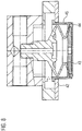
- Fig. 8 shows a cross section of a sucker 41.
- the specific action of this sucker can be discerned in this illustration. Since, in the case of the discs to be picked up, primarily in the case of the sensor carrier out discs 3, it is important that they be transported and applied absolutely in a flat position, in the case of each sucker head the area by which the respective disc is touched by the respective sucker head must be absolutely flat as well. This is achieved by virtue of the fact that, in the illustration shown, the sealing ring 44 is in a sucker head 45 composed of solid material. In this case, the sucker head 45 slides together with the rubber bellows 43 in the holding plate 42.
- the sucker head 45 can in this case for example also be approximately square or have any other surface shape which induces as little mechanical stress as possible in the disc respectively picked up.
- an elliptically shaped surface can contribute to reducing the stresses during picking-up and transport in the respective disc.
- Fig. 9 offers an explanatory illustration of an adhesive-bonding process.
- Fig. 9a here a detail view of the circumferential edge of a module frame 1 can be seen, which is a circular detail view at one location.
- the edge of a module frame 1 and the adjacent application of a silicone bead 6 can be discerned in detail.
- An acrylic spot 46 can be seen closely alongside said silicone seal 6.
- Fig. 9b additionally shows an acrylic application device 47 and a silicone application device 48 in a side view.
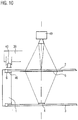
- Fig. 10 offers an explanatory illustration of the fixing of a sensor carrier disc 3.
- a sensor carrier disc 3 and a lens disc 2 here an acrylic spot 46 and the silicone seal 6 are shown.
- a sucker carrier 39 and a UV light emitter 40 are illustrated in a stylized manner on the left-hand side.
- the lens disc 2 is aligned, and then fixed by means of the curing of corresponding acrylic spots 46, such that the midpoints of all the Fresnel lenses 5 are directed exactly at the centre of the corresponding CPV sensors.
- This alignment can be effected purely optically by the lens disc 2 being adjusted in such a way that the position of the optical axis of its Fresnel lenses 5 impinges on the geometrical midpoint of corresponding CPV sensors.
- this alignment can also be effected in some other way, namely such that voltage is applied to selected CPV sensors themselves, whereupon the light emitted by them via the Fresnel lenses is detected and the lens disc 2 is adjusted in such a way that the emission of particular strategically important Fresnel lenses 5 becomes a maximum.
- a device for detecting the respective disc position of a lens disc 2 relative to the position of the sensor carrier disc 3 and for detecting the positioning mechanisms is necessary for this purpose. Such devices are familiar to the person skilled in the art and therefore not illustrated.
- the control signals of such a device are used for driving the transfer robot 19 for sensor carrier discs 3.
Landscapes
- Photovoltaic Devices (AREA)
- Life Sciences & Earth Sciences (AREA)
- Engineering & Computer Science (AREA)
- Sustainable Development (AREA)
- Sustainable Energy (AREA)
Description
- In photovoltaics, for many years there have already been approaches for working with concentrated solar radiation. In this case, the radiation from the sun is concentrated by means of mirrors and/or lenses, and directed onto specific concentrator solar cells. Corresponding systems of concentrating photovoltaics (CPV) are currently being tested in the Spanish Solar Research Institute Instituto de Sistemas Fotovoltaicos de Concentracion (ISFOC) in Castile at Puertollano. They concentrate the sunlight using lenses or mirrors to four-hundred- to thousand-fold intensity before it impinges on small solar cells, which are significantly more efficient than traditional silicon solar cells. Manufacturers from many parts of the world have installed CPV modules on the test site there. Approximately a thousand modules are currently installed on the site. Researchers are developing return prognoses, inter alia, and testing long-term stability in order to facilitate the transition from development to the markets for this technology. Documents
WO2010/124078A andUS2010/175685A disclose photovoltaic devices. Globally only a small number of CPV installations have been in operation hitherto. Their total power of approximately 30 megawatts corresponds approximately to the power of three nuclear power stations. A recent study by the American Market Research Institute Greentechmedia Research predicts, however, that this technology will advance apace. Accordingly, the CPV power installed annually might be 1000 megawatts as early as in 2015. Under favourable conditions, one kilowatt-hour of electrical energy from CPV installations, according to a study by the Fraunhofer Institute for solar energy systems (ISE) in Freiburg, costs between 18 and 21 cents per kilowatt-hour. Further cost reductions through more efficient components and mature industrial production are firmly expected.
At the heart of the installations are the high-power solar cells, which at present are in use primarily in space, where for years they have already been supplying satellites and robots with power. Instead of silicon, these cells contain so-called compound semiconductors composed of gallium, indium, arsenic or phosphorus. They consist of a plurality of different semiconductor layers, each of which processes a different range of the sunlight spectrum, while traditional silicon cells can convert only a smaller portion of the sunlight spectrum into electrical power. The following prior art is cited from the patent literature. -
US 4 834 805 A discloses a photovoltaic power module comprising the following features.
An arrangement of photovoltaic semiconductor crystal cells, distributed in individual cell locations in a layered substrate, wherein they are enclosed by two electrically conductive layers and separated by means of an insulating layer. Furthermore, this module consists of a light-conveying layer composed of lenses, which is arranged at a distance from the layered substrate, wherein incident radiation is focused into the substrate in the light-conveying layer by means of the lens, and wherein the thickness of the lens layer, of the substrate layer and of the space therebetween is less than 2 inches.
DE 10 2006 007 472 A1 discloses a photovoltaic concentrator module comprising a lens plate and a baseplate, on which solar cells are accommodated, and a frame, wherein the frame, connecting the lens plate and the baseplate, is arranged circumferentially along the edge of the lens plate and the baseplate.
This known concentrator module is intended to be improved to the effect that it can be produced cost-effectively, has a long service life, and that it allows simple and flexible integration of additional components which cannot be accommodated, or can be accommodated only with difficulty, on the lens plate or the baseplate. Furthermore, the intention is to develop a method which makes it possible to produce such concentrator modules.
The problem stated here is solved by virtue of the fact that along the frame between the lens plate and the frame and/or the baseplate and the frame firstly at least one first sealing compound and/or adhesive compound and secondly at least one second sealing compound are arranged circumferentially at least on part of the length of the frame, wherein the two sealing and/or adhesive compounds differ with regard to their curing time and/or gas permeability. The invention refers to a a method for fixing a lens as recited inclaim 1. Further advantageous embodiments are recited in the dependent claims. -
Fig. 1 shows amodule frame 1 in plan view -
Fig. 2 shows a concentrator module in cross section -
Fig. 3 shows a lens disc having Fresnellenses 5 -
Fig. 4 shows an overview of a manufacturing installation according to the invention -
Fig. 5 shows a plan view of amount 30 -
Fig. 6 shows an illustration of a placement device -
Fig. 7 shows a cross section of asucker carrier 39 -
Fig. 8 shows a cross section of asucker 41 -
Fig. 9 shows an explanatory illustration of an adhesive-bonding process -
Fig. 10 shows an explanatory illustration of the fixing of a sensor carrier disc -
Fig. 1 shows a module frame (1) in plan view. The section A-A illustrates the viewing direction of the side view that can be seen inFig. 2 . The module frame is subdivided into the zones shown by means of transverse webs. -
Fig. 2 shows a concentrator module with its carrying module frame (1) in cross section in an enlarged illustration. Here it is respectively possible to discern alens disc 2 on the top side and a correspondingsensor carrier disc 3 as base disc on the underside. In this case, themodule frame 1 is illustrated in a manner interrupted in its transverse extent on each side, in order to be able to show the details shown in the true size relationships. In thelens disc 2, indications of the Fresnellenses 5 used are found on the right-hand side, and in the sensor carrier disc there are thecorresponding CPV sensors 4. InFig. 2 , the regions of the application of asilicone seal 6 are also clearly marked on the left-hand side. -
Fig. 3 shows a lens disc with all Fresnellenses 5 incorporated in this size of amodule frame 1. 3 of said Fresnellenses 5 are designated separately on the right-hand side. On the left-hand side, in the circles depicted, the illustration shows the connections of the ribbon cables which combine the entire current of theindividual CPV sensors 4 of each of the zones shown, and which are relayed in the centre along amodule frame 1. -
Fig. 4 offers an overview of a manufacturing installation for the industrial production of photovoltaic concentrator modules. - A
magazine 24 formodule frames 1 can be discerned at the top left corner ofFig. 4 . Adjacent thereto, a gantry repositioning device formodule frames 1 is furthermore designated by 25. Thegantry repositioning device 25 acceptsmodule frames 1 from themagazine 24 and passes them onto a placement device 9. A lifting table 8 with 5 planes is used in this case. This placement device 9 then places arespective module frame 1 onto amount 30, which are moved together on thetransverse conveyor 14 to theapparatus 15 for applying acrylic 46 andsilicone 6. Here acrylic spots and a corresponding silicone bead are applied to the respective top side of amodule frame 1. - A
sensor carrier disc 3 as baseplate is emplaced thereon. Themagazine 18 forsensor carrier discs 3, thetransfer robot 19 forsensor carrier discs 3 and theplacement device 16 forsensor carrier discs 3 participate in this process. Thesensor carrier disc 3 is pressed with a predetermined contact pressure by means of theapparatus 16, starting centrally on the respective disc, and then fixed to themodule frame 1 by the curing of the acrylic spots by means of UV light. Such a fixing cannot be inferred from the prior art. The corresponding production processes will be explained in greater detail later. - The
mount 30 with themodule carrier 1 equipped in this way is moved to the location for mechanical, or else - depending on the development stage - automatic, contact-making 13, where the module frame is removed from themount 30, rotated from the horizontal position into a vertical position, and conveyed for manual contact-making at thestation 12. A distribution box for the electrical connecting lines is essentially incorporated here. The following electrical connection of the CPV sensors to the distribution box can be effected manually or automatically. Afterwards, themodule frame 1 is rotated into a horizontal position again, such that thesensor carrier disc 3 is at the bottom, and is fixed on amount 30. - The
mount 30 with themodule carrier 1 equipped in this way is then moved to theapparatus 15 for applying acrylic 46 andsilicone 6. Acrylic spots and a corresponding silicone bead are applied here. - A
lens disc 2 is emplaced thereon. The magazine forlens discs 22, thetransfer robot 20 for lens discs and theplacement device 17 for lens discs participate in this process. The corresponding production processes will be explained in greater detail later. The individual processing stations are equipped with lifting tables 11. Said lifting tables 11 serve for frictionlessly transportingmounts 30 andmodule carriers 1 during the operating sequence and enable components to be temporarily shifted into an intermediate storey. - An exact alignment of the
Fresnel lenses 5 with thecorresponding CPV sensors 4 is necessary for a completely satisfactory function of the concentrator module. Thelens discs 2 are adjusted by means of a camera (49). The technical process in this respect will be explained later. - After the fine adjustment of a
lens disc 2, thelens disc 2 is fixed by means of the curing of the acrylic spots by irradiation using a UV light emitter 40 (cf.Fig. 6 ). - The
mount 30 is then moved to thestation 10, where it is brought to a vertical position. The excess silicone is then removed manually or automatically from the vertically orientedmount 30. - From the
station 10, themount 30 treated in this way is moved by means of thetransverse conveyer 14 to a quality inspection. - After the quality inspection, the corresponding
mount 30 is moved into thestorage station 26, which has places in a plurality of planes, a plane for empty pallets also being provided. Here the silicone has the necessary time to be able to cure. - After the curing time, each concentrator module is provided with a barcode and brought by means of a lifting table 27 and a
gantry repositioning device 28 to stackingstations 29, which allow classification according to quality levels. -
Fig. 5 shows a plan view of amount 30. The dashed lines identify here anemplaced module frame 1. In this case, themodule frame 1 is fixed on the upper longitudinal side by means of thesame clamping elements 31 as those designated in detail at the lower longitudinal side. A clampingbar 37 is provided on the left broad side in the centre, at the location of the reinforced central web of themodule frame 1, said clamping bar corresponding to the two clampingbars 37 designated on the right broad side. These clamping bars have a conically bevelled sliding surface enabling accurately fitting insertion and easy removal of amodule frame 1 from above by means of a gripper. The functional principle of a clamping device can be discerned by way of example in the detail illustration depicted in an enlarged view in a circle. The upper half of said circle shows the bottom right corner of themodule frame 1 in an enlarged view. The clampingelement 31, which is likewise in an enlarged view and is of approximately square design, reveals a switchingrod 32 common to all 4clamping elements 31 on this side. The operative principle realized here will be explained in greater detail below. - An
eccentric disc 35 is seated on said switchingrod 32 and engages on a bevelledspline 33, which is in turn connected via two compression springs 34 to astop element 37, which presses onto themodule frame 1. If the switchingrod 32 is displaced, in this case towards the left, theeccentric disc 35 is also displaced towards the left and, in a manner sliding along thespline 33, compresses the compression springs 34, which transmit this pressure elastically to themodule frame 1. The twomagnets 36 join together and thus fix this basic setting, for example. - This basic setting can be performed manually or in an automated manner.
- For an automated displacement of the switching
rod 32, many possibilities are known to the person skilled in the art and so they will not be described in greater detail. - A further adjustment possibility for this arrangement, illustrated in principle, consists in rotating the switching
rod 32 and thus performing an additional setting, in particular a fine setting, by means of the rotation of theeccentric disc 35. - This can also be performed manually or in an automated manner.
- For the purpose of an automated setting, by means of the
servomotor 50 illustrated, on the right-hand side of a clampingelement 31, the switchingrod 32 can be rotated, in addition to the displacement described, at the designated location. The sleeve shown on the other side of a clampingelement 31 serves for the production engineering assembly of the switchingrod 32.Such servomotors 50 are situated on each clampingelement 31 in this case. This adjustment option makes it possible, in addition to a specific basic setting, whether it then be performed manually or in an automated manner, to set the contact pressure of each clampingelement 31 individually in an automated manner. By means of corresponding distance sensors and corresponding pressure sensors, which are not shown and designated here for reasons of clarity in the illustration, the same individual contact pressure can thus be set at each location of the longitudinal side of amodule frame 1 by means of said clampingelements 31. Thesame clamping elements 31 with the apparatuses described are incorporated on the other longitudinal side. This measure has the effect that even very slight deformations of the side walls of amodule frame 1 can be automatically taken into account during the clamping, and so a totally stress-free mounting of amodule frame 1 is ensured, and alens disc 2 and asensor carrier disc 3 can therefore in each case be combined with amodule frame 1 in a manner totally free of stress. This measure ensures that the forces which act on the adhesive bond of these discs in the event of large temperature differences can be minimized. This results in very little loading on the adhesive bond of a concentrator module and in an increase in its service life even under difficult climatic requirements. -
Fig. 6 shows an illustration of a placement device, having in eachcase 5sucker carriers 39, as part of a transfer process by means of atransfer robot 19 forsensor carrier discs 3, or by means of atransfer robot 20 forlens discs 2. In this case, a transfer robot generally has 4 sucker carriers on one side, by means of which carriers it picks up a respective disc on one side and transfers it to a placement device. A placement device generally has 5sucker carriers 39. The transfer of a disc by means of a transfer robot is effected by a procedure in which the disc is held on one side by means of 4 sucker carriers, and is inserted by the transfer robot into the 4 interspaces of a sucker carrier of a transfer unit having 5sucker carriers 39, and it is then sucked up on both sides by the transfer unit. Saidsucker carriers 39 in each case carrysuckers 41 and UVlight emitters 40 at their two ends, wherein UVlight emitters 40 are also fitted in each case in the centre of asucker carrier 39. -
Fig. 7 shows a cross section of asucker carrier 39. In addition to the illustration inFig. 6 , asensor carrier disc 2 that has been picked up is shown here. The twoUV light emitters 40 on the left and right can be discerned here in cross section. The central UVlight emitters 40 are concealed. -
Fig. 8 shows a cross section of asucker 41. The specific action of this sucker can be discerned in this illustration. Since, in the case of the discs to be picked up, primarily in the case of the sensor carrier outdiscs 3, it is important that they be transported and applied absolutely in a flat position, in the case of each sucker head the area by which the respective disc is touched by the respective sucker head must be absolutely flat as well. This is achieved by virtue of the fact that, in the illustration shown, the sealingring 44 is in asucker head 45 composed of solid material. In this case, thesucker head 45 slides together with the rubber bellows 43 in the holdingplate 42. Undulatory warpage of the picked-up disc at the locations of the engagement points of the respective suckers, as should be feared in other embodiments in the prior art with a flexible sealing lip, is ruled out in this case. Thesucker head 45 can in this case for example also be approximately square or have any other surface shape which induces as little mechanical stress as possible in the disc respectively picked up. Thus, for example, in this context, an elliptically shaped surface can contribute to reducing the stresses during picking-up and transport in the respective disc. -
Fig. 9 offers an explanatory illustration of an adhesive-bonding process. InFig. 9a , here a detail view of the circumferential edge of amodule frame 1 can be seen, which is a circular detail view at one location. Here the edge of amodule frame 1 and the adjacent application of asilicone bead 6 can be discerned in detail. Anacrylic spot 46 can be seen closely alongside saidsilicone seal 6. -
Fig. 9b additionally shows anacrylic application device 47 and asilicone application device 48 in a side view. -
Fig. 10 offers an explanatory illustration of the fixing of asensor carrier disc 3. Besides part of the cross section of amodule frame 1, asensor carrier disc 3 and alens disc 2, here anacrylic spot 46 and thesilicone seal 6 are shown. Asucker carrier 39 and aUV light emitter 40 are illustrated in a stylized manner on the left-hand side. By means of acamera 49, thelens disc 2 is aligned, and then fixed by means of the curing of correspondingacrylic spots 46, such that the midpoints of all theFresnel lenses 5 are directed exactly at the centre of the corresponding CPV sensors. - This alignment can be effected purely optically by the
lens disc 2 being adjusted in such a way that the position of the optical axis of itsFresnel lenses 5 impinges on the geometrical midpoint of corresponding CPV sensors. - However, this alignment can also be effected in some other way, namely such that voltage is applied to selected CPV sensors themselves, whereupon the light emitted by them via the Fresnel lenses is detected and the
lens disc 2 is adjusted in such a way that the emission of particular strategicallyimportant Fresnel lenses 5 becomes a maximum. A device for detecting the respective disc position of alens disc 2 relative to the position of thesensor carrier disc 3 and for detecting the positioning mechanisms is necessary for this purpose. Such devices are familiar to the person skilled in the art and therefore not illustrated. The control signals of such a device are used for driving thetransfer robot 19 forsensor carrier discs 3. - The control of the complex movement processes and the signal processing of the sensors used require a specific control program.
-
- 1
- Module frame
- 2
- Lens disc
- 3
- Sensor carrier disc (baseplate)
- 4
- CPV sensors
- 5
- Fresnel lenses
- 6
- Silicone seal
- 7
- Test station for seal testing, labelling
- 8
- Front lifting table for the mount (5 planes) cf. 27
- 9
- Placement device for module frames (on mount)
- 10
- Station for post-processing (silicone removal)
- 11
- Lifting tables of the processing stations (2 planes)
- 12
- Station for manual contact-making (processing)
- 13
- Station for mechanical, automatic contact-making
- 14
- Transverse conveying device for mounts
- 15
- Apparatus for applying acrylic and silicone
- 16
- Placement device for a
sensor carrier disc 3 - 17
- Placement device for the
lens disc 2 - 18
- Magazine for sensor carrier discs
- 19
- Transfer robot for sensor carrier discs
- 20
- Transfer robot for lens discs
- 21
- Suction gripper for sensor carrier discs (robot transfer)
- 22
- Magazine for lens discs
- 23
- Suction gripper for lens discs (robot transfer)
- 24
- Magazine for module frames
- 25
- Gantry repositioning device for module frames
- 26
- Storage stations (4 planes)
- 27
- Rear lifting table for mounts (5 planes) cf. 8
- 28
- Gantry repositioning device for final stacking (4 stations)
- 29
- Stacking stations (4 quality levels)
- 30
- Mount as carrier for
module frame 1 - 31
- Clamping element
- 32
- Switching rod
- 33
- Spline
- 34
- Compression spring
- 35
- Eccentric disc
- 36
- Magnet
- 37
- Stop element
- 38
- Clamping bar
- 39
- Sucker carrier
- 40
- UV light emitter
- 41
- Sucker
- 42
- Holding plate
- 43
- Rubber bellows
- 44
- Sealing ring
- 45
- Sucker head
- 46
- Acrylic
- 47
- Acrylic application device
- 48
- Silicone application device
- 49
- Camera
- 50
- servomotor
Claims (12)
- Method for fixing a lens disc (2) of a photovoltaic concentrator module comprising a sensor carrier disc (3) with CPV sensors (4) and a lens disc (2) with Fresnel lenses (5) sandwiching a module frame (1), comprising the steps of:a) Aligning the lens disc (2) by means of a camera (49) with the sensor carrier disc,b) Fixing the lens disc on the module frame (1), wherein fixing the lens disc (2) on the frame module is performed by means of curing of acrylic spots.
- Method according to claim 1, wherein the lens disc is aligned such that the midpoints of the Fresnel lenses (5) are directed at the centre of the corresponding concentrating photovoltaic (CPV) sensor.
- Method according to claim 1 or 2, wherein the acrylic spots are cured using a UV light emitter (40).
- Method according to claim 3, wherein the UV light emitters are incorporated in a placement device (17) used for placing the lens disc on the module frame (1) and aligning the lens disc.
- Method according to one of claims 1 to 4, wherein acrylic spots (46) and silicone beads (6) are applied on the module frame (1) before step a).
- Method according to claim 5, wherein the acrylic spots (46) and silicone beads (6) are applied by one apparatus (15) for applying acrylic (46) and silicone (6).
- Method according to claim 6, wherein fourteen acrylic spots (46) are provided per lens disc (2).
- Method according to one of claims 1 to 7 further comprising, before steps a) and b) the steps of:c) Placing a module frame (1) onto a mount (30) and moving them together to an apparatus (15) for applying acrylic (46) and silicon (6) to apply acrylic spots and a corresponding silicone bead to the respective top side of the module frame (1), thend) Placing a sensor carrier disc (3) thereon, pressing the sensor carrier disc with a predetermined contact pressure, in particular starting centrally, and then fixing the sensor carrier disc (3) to the module frame by the curing of the acrylic spots by means of UV light, thene) rotating the module frame (1)into a horizontal position such that the sensor carrier disc (3) is at the bottom, thenf) applying acrylic (46) and silicone (6) on the module frame, and theng) placing a lens disc (2) thereon.
- Method according to claim 8, wherein step g), a) and b) are realized one after the other using the placement device with the UV light emitters.
- Method according to claim 9, further comprising, between step d) and e) the step h) of moving the mount (30) with the module frame to a location for mechanical or automatic contact making.
- Method according to one of claims 8 to 10, wherein twelve sensor carrier discs (3) are mount on one module frame (1).
- Method according to one of claims 1 to 11, wherein the alignment step is carried out purely optically by the lens disc (2) being adjusted in such a way that the position of the optical axis of the Fresnel lenses (5) impinges on the geometrical midpoint of corresponding CPV sensors.
Applications Claiming Priority (3)
| Application Number | Priority Date | Filing Date | Title |
|---|---|---|---|
| DE202011108836U DE202011108836U1 (en) | 2011-12-08 | 2011-12-08 | Apparatus for the industrial production of photovoltaic concentrator modules |
| DE202011109424U DE202011109424U1 (en) | 2011-12-23 | 2011-12-23 | Device for industrial wiring and final testing of photovoltaic concentrator modules |
| PCT/EP2012/005070 WO2013083284A1 (en) | 2011-12-08 | 2012-12-07 | Apparatus for the industrial production of photovoltaic concentrator modules |
Publications (2)
| Publication Number | Publication Date |
|---|---|
| EP2789016A1 EP2789016A1 (en) | 2014-10-15 |
| EP2789016B1 true EP2789016B1 (en) | 2018-03-07 |
Family
ID=47520001
Family Applications (2)
| Application Number | Title | Priority Date | Filing Date |
|---|---|---|---|
| EP12812162.1A Not-in-force EP2789014B1 (en) | 2011-12-08 | 2012-12-07 | Concentrating photovoltaic cell array |
| EP12812520.0A Not-in-force EP2789016B1 (en) | 2011-12-08 | 2012-12-07 | Method for the industrial production of photovoltaic concentrator modules |
Family Applications Before (1)
| Application Number | Title | Priority Date | Filing Date |
|---|---|---|---|
| EP12812162.1A Not-in-force EP2789014B1 (en) | 2011-12-08 | 2012-12-07 | Concentrating photovoltaic cell array |
Country Status (6)
| Country | Link |
|---|---|
| US (2) | US9640696B2 (en) |
| EP (2) | EP2789014B1 (en) |
| CN (2) | CN104025316B (en) |
| ES (2) | ES2728441T3 (en) |
| FR (2) | FR2984011B1 (en) |
| WO (2) | WO2013083283A1 (en) |
Families Citing this family (8)
| Publication number | Priority date | Publication date | Assignee | Title |
|---|---|---|---|---|
| WO2013083283A1 (en) | 2011-12-08 | 2013-06-13 | Soitec Solar Gmbh | Concentrating photovoltaic cell array |
| DE102016003486B4 (en) * | 2016-03-24 | 2021-04-22 | Azur Space Solar Power Gmbh | Solar cell unit and solar cell module |
| DE102016003487B4 (en) * | 2016-03-24 | 2020-03-12 | Azur Space Solar Power Gmbh | Solar cell unit and solar cell module |
| DE102016011321A1 (en) | 2016-09-21 | 2018-03-22 | Azur Space Solar Power Gmbh | solar cell module |
| ES2663571B1 (en) * | 2016-10-10 | 2019-01-15 | Fund Cener Ciemat | MIRROR FOR SOLAR REFLECTOR AND ASSEMBLY PROCEDURE |
| US10972047B2 (en) * | 2017-02-27 | 2021-04-06 | International Business Machines Corporation | Photovoltaic module |
| CN107919406B (en) * | 2017-10-25 | 2019-11-12 | 华北电力大学 | A Dense Concentrating Photovoltaic Cell Array with Reduced Mismatch Loss |
| CN112087193B (en) * | 2020-09-21 | 2022-08-23 | 华能太仓发电有限责任公司 | Solar panel edge fixing mechanism |
Family Cites Families (21)
| Publication number | Priority date | Publication date | Assignee | Title |
|---|---|---|---|---|
| US4258698A (en) * | 1979-09-10 | 1981-03-31 | Sales Franklin D | Solar heating apparatus |
| US4285698A (en) * | 1980-04-28 | 1981-08-25 | Peanut Research & Testing Laboratories, Inc. | Analysis of aflatoxins in peanuts by high pressure liquid chromatograph |
| US4834805A (en) | 1987-09-24 | 1989-05-30 | Wattsun, Inc. | Photovoltaic power modules and methods for making same |
| US6248948B1 (en) * | 1998-05-15 | 2001-06-19 | Canon Kabushiki Kaisha | Solar cell module and method of producing the same |
| JP2000036613A (en) * | 1998-05-15 | 2000-02-02 | Canon Inc | Solar cell module and method of manufacturing the same |
| JP2002289900A (en) * | 2001-03-23 | 2002-10-04 | Canon Inc | Concentrating solar cell module and concentrating solar power generation system |
| US20050072456A1 (en) * | 2003-01-23 | 2005-04-07 | Stevenson Edward J. | Integrated photovoltaic roofing system |
| US7342171B2 (en) * | 2003-01-23 | 2008-03-11 | Solar Intergrated Technologies, Inc. | Integrated photovoltaic roofing component and panel |
| DE102006007472B4 (en) | 2006-02-17 | 2018-03-22 | Fraunhofer-Gesellschaft zur Förderung der angewandten Forschung e.V. | Photovoltaic concentrator module with multifunctional frame |
| CN200989672Y (en) * | 2006-05-22 | 2007-12-12 | 夏秋 | High-performance solar energy device |
| US7521630B2 (en) * | 2007-03-01 | 2009-04-21 | Ball Newton E | Parallel and virtual parallel interconnection of solar cells in solar panels |
| KR20090081950A (en) * | 2008-01-25 | 2009-07-29 | 삼성전자주식회사 | Solar cell and manufacturing method thereof |
| JP2009182244A (en) * | 2008-01-31 | 2009-08-13 | Sharp Corp | Manufacturing method of solar cell module |
| US20100175685A1 (en) | 2008-07-14 | 2010-07-15 | Robert Owen Campbell | Advanced Tracking Concentrator Employing Rotating Input Arrangement and Method |
| EP2422375A2 (en) * | 2009-04-24 | 2012-02-29 | Peumans, Peter | Photovoltaic arrays, micro-concentrator solar cells and modules and methods of making |
| DE102009044610A1 (en) | 2009-11-20 | 2011-05-26 | Azur Space Solar Power Gmbh | solar cell module |
| DE102009060604A1 (en) | 2009-12-23 | 2011-06-30 | Energetica Holding Gmbh | Solar module with a printed circuit board and method of manufacture and application |
| DE102010016675A1 (en) | 2010-04-28 | 2011-11-03 | Solarworld Innovations Gmbh | Photovoltaic module, method for electrically connecting a plurality of photovoltaic cells, and means for electrically connecting a plurality of photovoltaic cells |
| DE202011108836U1 (en) | 2011-12-08 | 2011-12-29 | Grenzebach Maschinenbau Gmbh | Apparatus for the industrial production of photovoltaic concentrator modules |
| WO2013083283A1 (en) | 2011-12-08 | 2013-06-13 | Soitec Solar Gmbh | Concentrating photovoltaic cell array |
| JP5762377B2 (en) | 2012-09-28 | 2015-08-12 | 太陽誘電株式会社 | Impedance matching circuit and antenna system |
-
2012
- 2012-12-07 WO PCT/EP2012/005069 patent/WO2013083283A1/en not_active Ceased
- 2012-12-07 FR FR1261800A patent/FR2984011B1/en not_active Expired - Fee Related
- 2012-12-07 US US14/361,149 patent/US9640696B2/en not_active Expired - Fee Related
- 2012-12-07 ES ES12812162T patent/ES2728441T3/en active Active
- 2012-12-07 EP EP12812162.1A patent/EP2789014B1/en not_active Not-in-force
- 2012-12-07 WO PCT/EP2012/005070 patent/WO2013083284A1/en not_active Ceased
- 2012-12-07 FR FR1261799A patent/FR2984012B1/en not_active Expired - Fee Related
- 2012-12-07 ES ES12812520.0T patent/ES2668501T3/en active Active
- 2012-12-07 CN CN201280060414.2A patent/CN104025316B/en not_active Expired - Fee Related
- 2012-12-07 EP EP12812520.0A patent/EP2789016B1/en not_active Not-in-force
- 2012-12-07 CN CN201280060521.5A patent/CN104106212B/en not_active Expired - Fee Related
- 2012-12-07 US US14/361,265 patent/US10103284B2/en active Active
Also Published As
| Publication number | Publication date |
|---|---|
| WO2013083284A1 (en) | 2013-06-13 |
| CN104106212B (en) | 2018-07-13 |
| EP2789016A1 (en) | 2014-10-15 |
| ES2668501T3 (en) | 2018-05-18 |
| EP2789014A1 (en) | 2014-10-15 |
| US20140299176A1 (en) | 2014-10-09 |
| CN104025316A (en) | 2014-09-03 |
| EP2789014B1 (en) | 2019-03-27 |
| FR2984011B1 (en) | 2016-12-16 |
| ES2728441T3 (en) | 2019-10-24 |
| US20140331472A1 (en) | 2014-11-13 |
| CN104025316B (en) | 2017-06-09 |
| FR2984012B1 (en) | 2016-12-09 |
| FR2984012A1 (en) | 2013-06-14 |
| US9640696B2 (en) | 2017-05-02 |
| WO2013083283A1 (en) | 2013-06-13 |
| FR2984011A1 (en) | 2013-06-14 |
| US10103284B2 (en) | 2018-10-16 |
| CN104106212A (en) | 2014-10-15 |
Similar Documents
| Publication | Publication Date | Title |
|---|---|---|
| US10103284B2 (en) | Apparatus for the industrial production of photovoltaic concentrator modules | |
| US9190554B2 (en) | Method and device for industrially producing photovoltaic concentrator modules | |
| US9899559B2 (en) | System and method for producing modular photovoltaic panel assemblies for space solar arrays | |
| US10056522B2 (en) | System and apparatus for precision automation of tab attachment for fabrications of solar panels | |
| CN107256908B (en) | Continuous production process of battery string array of solar modules and its production equipment | |
| KR101656354B1 (en) | The solar cell production system | |
| TWI648946B (en) | Method of manufacturing space grade solar arrays | |
| KR101656344B1 (en) | The stringer | |
| US20080037141A1 (en) | Method for alignment of optical elements in an array | |
| CN115639211B (en) | Automatic high-speed detection equipment for battery cover plate | |
| KR101744564B1 (en) | Method and Apparatus for assembling Solar cell module | |
| CN206293457U (en) | Equipment and system for manufacturing solar cell for processing solar cell | |
| JP6113749B2 (en) | Method and apparatus for industrial wiring and final inspection of photovoltaic concentrator modules | |
| KR101939490B1 (en) | Laminator for curved solar battery | |
| US20260114071A1 (en) | Tabbing device and tabbing method | |
| CN222912673U (en) | A fully automatic visual inspection device for water cooling panels | |
| CN121263027A (en) | Laminating equipment of perovskite photovoltaic module | |
| CN116364802A (en) | Preparation method of photovoltaic module and lamination equipment for photovoltaic module | |
| KR20130049971A (en) | In-line type substrate processing system |
Legal Events
| Date | Code | Title | Description |
|---|---|---|---|
| PUAI | Public reference made under article 153(3) epc to a published international application that has entered the european phase |
Free format text: ORIGINAL CODE: 0009012 |
|
| 17P | Request for examination filed |
Effective date: 20140606 |
|
| AK | Designated contracting states |
Kind code of ref document: A1 Designated state(s): AL AT BE BG CH CY CZ DE DK EE ES FI FR GB GR HR HU IE IS IT LI LT LU LV MC MK MT NL NO PL PT RO RS SE SI SK SM TR |
|
| DAX | Request for extension of the european patent (deleted) | ||
| RAP1 | Party data changed (applicant data changed or rights of an application transferred) |
Owner name: SAINT-AUGUSTIN CANADA ELECTRIC INC. |
|
| GRAP | Despatch of communication of intention to grant a patent |
Free format text: ORIGINAL CODE: EPIDOSNIGR1 |
|
| INTG | Intention to grant announced |
Effective date: 20170926 |
|
| GRAS | Grant fee paid |
Free format text: ORIGINAL CODE: EPIDOSNIGR3 |
|
| GRAA | (expected) grant |
Free format text: ORIGINAL CODE: 0009210 |
|
| AK | Designated contracting states |
Kind code of ref document: B1 Designated state(s): AL AT BE BG CH CY CZ DE DK EE ES FI FR GB GR HR HU IE IS IT LI LT LU LV MC MK MT NL NO PL PT RO RS SE SI SK SM TR |
|
| REG | Reference to a national code |
Ref country code: GB Ref legal event code: FG4D |
|
| REG | Reference to a national code |
Ref country code: CH Ref legal event code: EP Ref country code: AT Ref legal event code: REF Ref document number: 977418 Country of ref document: AT Kind code of ref document: T Effective date: 20180315 |
|
| REG | Reference to a national code |
Ref country code: IE Ref legal event code: FG4D |
|
| REG | Reference to a national code |
Ref country code: DE Ref legal event code: R096 Ref document number: 602012043816 Country of ref document: DE |
|
| REG | Reference to a national code |
Ref country code: ES Ref legal event code: FG2A Ref document number: 2668501 Country of ref document: ES Kind code of ref document: T3 Effective date: 20180518 |
|
| REG | Reference to a national code |
Ref country code: NL Ref legal event code: MP Effective date: 20180307 |
|
| REG | Reference to a national code |
Ref country code: LT Ref legal event code: MG4D |
|
| PG25 | Lapsed in a contracting state [announced via postgrant information from national office to epo] |
Ref country code: CY Free format text: LAPSE BECAUSE OF FAILURE TO SUBMIT A TRANSLATION OF THE DESCRIPTION OR TO PAY THE FEE WITHIN THE PRESCRIBED TIME-LIMIT Effective date: 20180307 Ref country code: FI Free format text: LAPSE BECAUSE OF FAILURE TO SUBMIT A TRANSLATION OF THE DESCRIPTION OR TO PAY THE FEE WITHIN THE PRESCRIBED TIME-LIMIT Effective date: 20180307 Ref country code: LT Free format text: LAPSE BECAUSE OF FAILURE TO SUBMIT A TRANSLATION OF THE DESCRIPTION OR TO PAY THE FEE WITHIN THE PRESCRIBED TIME-LIMIT Effective date: 20180307 Ref country code: HR Free format text: LAPSE BECAUSE OF FAILURE TO SUBMIT A TRANSLATION OF THE DESCRIPTION OR TO PAY THE FEE WITHIN THE PRESCRIBED TIME-LIMIT Effective date: 20180307 Ref country code: NO Free format text: LAPSE BECAUSE OF FAILURE TO SUBMIT A TRANSLATION OF THE DESCRIPTION OR TO PAY THE FEE WITHIN THE PRESCRIBED TIME-LIMIT Effective date: 20180607 |
|
| REG | Reference to a national code |
Ref country code: AT Ref legal event code: MK05 Ref document number: 977418 Country of ref document: AT Kind code of ref document: T Effective date: 20180307 |
|
| PG25 | Lapsed in a contracting state [announced via postgrant information from national office to epo] |
Ref country code: BG Free format text: LAPSE BECAUSE OF FAILURE TO SUBMIT A TRANSLATION OF THE DESCRIPTION OR TO PAY THE FEE WITHIN THE PRESCRIBED TIME-LIMIT Effective date: 20180607 Ref country code: RS Free format text: LAPSE BECAUSE OF FAILURE TO SUBMIT A TRANSLATION OF THE DESCRIPTION OR TO PAY THE FEE WITHIN THE PRESCRIBED TIME-LIMIT Effective date: 20180307 Ref country code: GR Free format text: LAPSE BECAUSE OF FAILURE TO SUBMIT A TRANSLATION OF THE DESCRIPTION OR TO PAY THE FEE WITHIN THE PRESCRIBED TIME-LIMIT Effective date: 20180608 Ref country code: SE Free format text: LAPSE BECAUSE OF FAILURE TO SUBMIT A TRANSLATION OF THE DESCRIPTION OR TO PAY THE FEE WITHIN THE PRESCRIBED TIME-LIMIT Effective date: 20180307 Ref country code: LV Free format text: LAPSE BECAUSE OF FAILURE TO SUBMIT A TRANSLATION OF THE DESCRIPTION OR TO PAY THE FEE WITHIN THE PRESCRIBED TIME-LIMIT Effective date: 20180307 |
|
| PG25 | Lapsed in a contracting state [announced via postgrant information from national office to epo] |
Ref country code: RO Free format text: LAPSE BECAUSE OF FAILURE TO SUBMIT A TRANSLATION OF THE DESCRIPTION OR TO PAY THE FEE WITHIN THE PRESCRIBED TIME-LIMIT Effective date: 20180307 Ref country code: PL Free format text: LAPSE BECAUSE OF FAILURE TO SUBMIT A TRANSLATION OF THE DESCRIPTION OR TO PAY THE FEE WITHIN THE PRESCRIBED TIME-LIMIT Effective date: 20180307 Ref country code: NL Free format text: LAPSE BECAUSE OF FAILURE TO SUBMIT A TRANSLATION OF THE DESCRIPTION OR TO PAY THE FEE WITHIN THE PRESCRIBED TIME-LIMIT Effective date: 20180307 Ref country code: AL Free format text: LAPSE BECAUSE OF FAILURE TO SUBMIT A TRANSLATION OF THE DESCRIPTION OR TO PAY THE FEE WITHIN THE PRESCRIBED TIME-LIMIT Effective date: 20180307 Ref country code: EE Free format text: LAPSE BECAUSE OF FAILURE TO SUBMIT A TRANSLATION OF THE DESCRIPTION OR TO PAY THE FEE WITHIN THE PRESCRIBED TIME-LIMIT Effective date: 20180307 |
|
| PG25 | Lapsed in a contracting state [announced via postgrant information from national office to epo] |
Ref country code: AT Free format text: LAPSE BECAUSE OF FAILURE TO SUBMIT A TRANSLATION OF THE DESCRIPTION OR TO PAY THE FEE WITHIN THE PRESCRIBED TIME-LIMIT Effective date: 20180307 Ref country code: SM Free format text: LAPSE BECAUSE OF FAILURE TO SUBMIT A TRANSLATION OF THE DESCRIPTION OR TO PAY THE FEE WITHIN THE PRESCRIBED TIME-LIMIT Effective date: 20180307 Ref country code: CZ Free format text: LAPSE BECAUSE OF FAILURE TO SUBMIT A TRANSLATION OF THE DESCRIPTION OR TO PAY THE FEE WITHIN THE PRESCRIBED TIME-LIMIT Effective date: 20180307 Ref country code: SK Free format text: LAPSE BECAUSE OF FAILURE TO SUBMIT A TRANSLATION OF THE DESCRIPTION OR TO PAY THE FEE WITHIN THE PRESCRIBED TIME-LIMIT Effective date: 20180307 |
|
| REG | Reference to a national code |
Ref country code: DE Ref legal event code: R097 Ref document number: 602012043816 Country of ref document: DE |
|
| PG25 | Lapsed in a contracting state [announced via postgrant information from national office to epo] |
Ref country code: PT Free format text: LAPSE BECAUSE OF FAILURE TO SUBMIT A TRANSLATION OF THE DESCRIPTION OR TO PAY THE FEE WITHIN THE PRESCRIBED TIME-LIMIT Effective date: 20180709 |
|
| PLBE | No opposition filed within time limit |
Free format text: ORIGINAL CODE: 0009261 |
|
| STAA | Information on the status of an ep patent application or granted ep patent |
Free format text: STATUS: NO OPPOSITION FILED WITHIN TIME LIMIT |
|
| PG25 | Lapsed in a contracting state [announced via postgrant information from national office to epo] |
Ref country code: DK Free format text: LAPSE BECAUSE OF FAILURE TO SUBMIT A TRANSLATION OF THE DESCRIPTION OR TO PAY THE FEE WITHIN THE PRESCRIBED TIME-LIMIT Effective date: 20180307 |
|
| 26N | No opposition filed |
Effective date: 20181210 |
|
| PG25 | Lapsed in a contracting state [announced via postgrant information from national office to epo] |
Ref country code: SI Free format text: LAPSE BECAUSE OF FAILURE TO SUBMIT A TRANSLATION OF THE DESCRIPTION OR TO PAY THE FEE WITHIN THE PRESCRIBED TIME-LIMIT Effective date: 20180307 |
|
| REG | Reference to a national code |
Ref country code: CH Ref legal event code: PL |
|
| GBPC | Gb: european patent ceased through non-payment of renewal fee |
Effective date: 20181207 |
|
| PG25 | Lapsed in a contracting state [announced via postgrant information from national office to epo] |
Ref country code: LU Free format text: LAPSE BECAUSE OF NON-PAYMENT OF DUE FEES Effective date: 20181207 Ref country code: MC Free format text: LAPSE BECAUSE OF FAILURE TO SUBMIT A TRANSLATION OF THE DESCRIPTION OR TO PAY THE FEE WITHIN THE PRESCRIBED TIME-LIMIT Effective date: 20180307 |
|
| REG | Reference to a national code |
Ref country code: IE Ref legal event code: MM4A |
|
| REG | Reference to a national code |
Ref country code: BE Ref legal event code: MM Effective date: 20181231 |
|
| PG25 | Lapsed in a contracting state [announced via postgrant information from national office to epo] |
Ref country code: IE Free format text: LAPSE BECAUSE OF NON-PAYMENT OF DUE FEES Effective date: 20181207 |
|
| PG25 | Lapsed in a contracting state [announced via postgrant information from national office to epo] |
Ref country code: BE Free format text: LAPSE BECAUSE OF NON-PAYMENT OF DUE FEES Effective date: 20181231 |
|
| PG25 | Lapsed in a contracting state [announced via postgrant information from national office to epo] |
Ref country code: CH Free format text: LAPSE BECAUSE OF NON-PAYMENT OF DUE FEES Effective date: 20181231 Ref country code: LI Free format text: LAPSE BECAUSE OF NON-PAYMENT OF DUE FEES Effective date: 20181231 Ref country code: GB Free format text: LAPSE BECAUSE OF NON-PAYMENT OF DUE FEES Effective date: 20181207 |
|
| PG25 | Lapsed in a contracting state [announced via postgrant information from national office to epo] |
Ref country code: MT Free format text: LAPSE BECAUSE OF NON-PAYMENT OF DUE FEES Effective date: 20181207 |
|
| PG25 | Lapsed in a contracting state [announced via postgrant information from national office to epo] |
Ref country code: TR Free format text: LAPSE BECAUSE OF FAILURE TO SUBMIT A TRANSLATION OF THE DESCRIPTION OR TO PAY THE FEE WITHIN THE PRESCRIBED TIME-LIMIT Effective date: 20180307 |
|
| PG25 | Lapsed in a contracting state [announced via postgrant information from national office to epo] |
Ref country code: HU Free format text: LAPSE BECAUSE OF FAILURE TO SUBMIT A TRANSLATION OF THE DESCRIPTION OR TO PAY THE FEE WITHIN THE PRESCRIBED TIME-LIMIT; INVALID AB INITIO Effective date: 20121207 Ref country code: MK Free format text: LAPSE BECAUSE OF NON-PAYMENT OF DUE FEES Effective date: 20180307 |
|
| PG25 | Lapsed in a contracting state [announced via postgrant information from national office to epo] |
Ref country code: IS Free format text: LAPSE BECAUSE OF FAILURE TO SUBMIT A TRANSLATION OF THE DESCRIPTION OR TO PAY THE FEE WITHIN THE PRESCRIBED TIME-LIMIT Effective date: 20180707 |
|
| PGFP | Annual fee paid to national office [announced via postgrant information from national office to epo] |
Ref country code: IT Payment date: 20231227 Year of fee payment: 12 Ref country code: FR Payment date: 20231220 Year of fee payment: 12 |
|
| PGFP | Annual fee paid to national office [announced via postgrant information from national office to epo] |
Ref country code: ES Payment date: 20240102 Year of fee payment: 12 |
|
| PGFP | Annual fee paid to national office [announced via postgrant information from national office to epo] |
Ref country code: DE Payment date: 20231221 Year of fee payment: 12 |
|
| REG | Reference to a national code |
Ref country code: DE Ref legal event code: R079 Ref document number: 602012043816 Country of ref document: DE Free format text: PREVIOUS MAIN CLASS: H01L0031023200 Ipc: H10F0077400000 |
|
| REG | Reference to a national code |
Ref country code: DE Ref legal event code: R119 Ref document number: 602012043816 Country of ref document: DE |
|
| PG25 | Lapsed in a contracting state [announced via postgrant information from national office to epo] |
Ref country code: DE Free format text: LAPSE BECAUSE OF NON-PAYMENT OF DUE FEES Effective date: 20250701 |
|
| PG25 | Lapsed in a contracting state [announced via postgrant information from national office to epo] |
Ref country code: IT Free format text: LAPSE BECAUSE OF NON-PAYMENT OF DUE FEES Effective date: 20241207 |
|
| PG25 | Lapsed in a contracting state [announced via postgrant information from national office to epo] |
Ref country code: FR Free format text: LAPSE BECAUSE OF NON-PAYMENT OF DUE FEES Effective date: 20241231 |
|
| REG | Reference to a national code |
Ref country code: ES Ref legal event code: FD2A Effective date: 20260128 |
|
| PG25 | Lapsed in a contracting state [announced via postgrant information from national office to epo] |
Ref country code: ES Free format text: LAPSE BECAUSE OF NON-PAYMENT OF DUE FEES Effective date: 20241208 |