EP2788720B1 - Electronic device comprising a moulded interconnect device - Google Patents
Electronic device comprising a moulded interconnect device Download PDFInfo
- Publication number
- EP2788720B1 EP2788720B1 EP12808866.3A EP12808866A EP2788720B1 EP 2788720 B1 EP2788720 B1 EP 2788720B1 EP 12808866 A EP12808866 A EP 12808866A EP 2788720 B1 EP2788720 B1 EP 2788720B1
- Authority
- EP
- European Patent Office
- Prior art keywords
- moulded
- interconnect device
- electronic device
- substrate
- interconnect
- Prior art date
- Legal status (The legal status is an assumption and is not a legal conclusion. Google has not performed a legal analysis and makes no representation as to the accuracy of the status listed.)
- Active
Links
Images


Classifications
-
- G—PHYSICS
- G01—MEASURING; TESTING
- G01C—MEASURING DISTANCES, LEVELS OR BEARINGS; SURVEYING; NAVIGATION; GYROSCOPIC INSTRUMENTS; PHOTOGRAMMETRY OR VIDEOGRAMMETRY
- G01C21/00—Navigation; Navigational instruments not provided for in groups G01C1/00 - G01C19/00
- G01C21/10—Navigation; Navigational instruments not provided for in groups G01C1/00 - G01C19/00 by using measurements of speed or acceleration
- G01C21/12—Navigation; Navigational instruments not provided for in groups G01C1/00 - G01C19/00 by using measurements of speed or acceleration executed aboard the object being navigated; Dead reckoning
- G01C21/16—Navigation; Navigational instruments not provided for in groups G01C1/00 - G01C19/00 by using measurements of speed or acceleration executed aboard the object being navigated; Dead reckoning by integrating acceleration or speed, i.e. inertial navigation
- G01C21/165—Navigation; Navigational instruments not provided for in groups G01C1/00 - G01C19/00 by using measurements of speed or acceleration executed aboard the object being navigated; Dead reckoning by integrating acceleration or speed, i.e. inertial navigation combined with non-inertial navigation instruments
-
- G—PHYSICS
- G01—MEASURING; TESTING
- G01S—RADIO DIRECTION-FINDING; RADIO NAVIGATION; DETERMINING DISTANCE OR VELOCITY BY USE OF RADIO WAVES; LOCATING OR PRESENCE-DETECTING BY USE OF THE REFLECTION OR RERADIATION OF RADIO WAVES; ANALOGOUS ARRANGEMENTS USING OTHER WAVES
- G01S19/00—Satellite radio beacon positioning systems; Determining position, velocity or attitude using signals transmitted by such systems
- G01S19/01—Satellite radio beacon positioning systems transmitting time-stamped messages, e.g. GPS [Global Positioning System], GLONASS [Global Orbiting Navigation Satellite System] or GALILEO
- G01S19/13—Receivers
-
- G—PHYSICS
- G01—MEASURING; TESTING
- G01S—RADIO DIRECTION-FINDING; RADIO NAVIGATION; DETERMINING DISTANCE OR VELOCITY BY USE OF RADIO WAVES; LOCATING OR PRESENCE-DETECTING BY USE OF THE REFLECTION OR RERADIATION OF RADIO WAVES; ANALOGOUS ARRANGEMENTS USING OTHER WAVES
- G01S19/00—Satellite radio beacon positioning systems; Determining position, velocity or attitude using signals transmitted by such systems
- G01S19/01—Satellite radio beacon positioning systems transmitting time-stamped messages, e.g. GPS [Global Positioning System], GLONASS [Global Orbiting Navigation Satellite System] or GALILEO
- G01S19/13—Receivers
- G01S19/35—Constructional details or hardware or software details of the signal processing chain
-
- G—PHYSICS
- G01—MEASURING; TESTING
- G01S—RADIO DIRECTION-FINDING; RADIO NAVIGATION; DETERMINING DISTANCE OR VELOCITY BY USE OF RADIO WAVES; LOCATING OR PRESENCE-DETECTING BY USE OF THE REFLECTION OR RERADIATION OF RADIO WAVES; ANALOGOUS ARRANGEMENTS USING OTHER WAVES
- G01S19/00—Satellite radio beacon positioning systems; Determining position, velocity or attitude using signals transmitted by such systems
- G01S19/38—Determining a navigation solution using signals transmitted by a satellite radio beacon positioning system
- G01S19/39—Determining a navigation solution using signals transmitted by a satellite radio beacon positioning system the satellite radio beacon positioning system transmitting time-stamped messages, e.g. GPS [Global Positioning System], GLONASS [Global Orbiting Navigation Satellite System] or GALILEO
- G01S19/42—Determining position
- G01S19/48—Determining position by combining or switching between position solutions derived from the satellite radio beacon positioning system and position solutions derived from a further system
- G01S19/49—Determining position by combining or switching between position solutions derived from the satellite radio beacon positioning system and position solutions derived from a further system whereby the further system is an inertial position system, e.g. loosely-coupled
-
- H—ELECTRICITY
- H05—ELECTRIC TECHNIQUES NOT OTHERWISE PROVIDED FOR
- H05K—PRINTED CIRCUITS; CASINGS OR CONSTRUCTIONAL DETAILS OF ELECTRIC APPARATUS; MANUFACTURE OF ASSEMBLAGES OF ELECTRICAL COMPONENTS
- H05K1/00—Printed circuits
- H05K1/02—Details
- H05K1/11—Printed elements for providing electric connections to or between printed circuits
- H05K1/119—Details of rigid insulating substrates therefor, e.g. three-dimensional details
-
- H—ELECTRICITY
- H05—ELECTRIC TECHNIQUES NOT OTHERWISE PROVIDED FOR
- H05K—PRINTED CIRCUITS; CASINGS OR CONSTRUCTIONAL DETAILS OF ELECTRIC APPARATUS; MANUFACTURE OF ASSEMBLAGES OF ELECTRICAL COMPONENTS
- H05K1/00—Printed circuits
- H05K1/02—Details
- H05K1/14—Structural association of two or more printed circuits
- H05K1/144—Stacked arrangements of planar printed circuit boards
-
- H—ELECTRICITY
- H05—ELECTRIC TECHNIQUES NOT OTHERWISE PROVIDED FOR
- H05K—PRINTED CIRCUITS; CASINGS OR CONSTRUCTIONAL DETAILS OF ELECTRIC APPARATUS; MANUFACTURE OF ASSEMBLAGES OF ELECTRICAL COMPONENTS
- H05K7/00—Constructional details common to different types of electric apparatus
- H05K7/02—Arrangements of circuit components or wiring on supporting structure
- H05K7/10—Plug-in assemblages of components, e.g. IC sockets
-
- H—ELECTRICITY
- H05—ELECTRIC TECHNIQUES NOT OTHERWISE PROVIDED FOR
- H05K—PRINTED CIRCUITS; CASINGS OR CONSTRUCTIONAL DETAILS OF ELECTRIC APPARATUS; MANUFACTURE OF ASSEMBLAGES OF ELECTRICAL COMPONENTS
- H05K2203/00—Indexing scheme relating to apparatus or processes for manufacturing printed circuits covered by H05K3/00
- H05K2203/16—Inspection; Monitoring; Aligning
- H05K2203/167—Using mechanical means for positioning, alignment or registration, e.g. using rod-in-hole alignment
Definitions
- This invention relates to an electronic device, and in particular to a device in which there is a need to accommodate a large quantity of components into a small volume, and so the device is packaged with high density.
- a key aspect in achieving compact multi-functional electronic devices is how to package and interconnect a large number of electronic components in a small volume.
- the orientation and position of specific components is critical.
- the components are transducers, for example in medical applications.
- the relative positions of components may further be significant, for example to ensure that sensitive analog components are shielded from high speed digital components.
- components are supported in a manner that is robust, for example that is capable of withstanding shock loads such as those arising from collisions (for example those that may arise in automotive contexts or due to dropping the device onto a hard surface).
- One example of an electronic device application that includes all the requirements set out above is in navigation systems. In such applications it is necessary to track the location or movement of an object relative to an inertial reference frame.
- Inertial navigation is one method by which this may be achieved, in which the change in position of an object is tracked by updating a known starting position and velocity based on measured accelerations of the object in the inertial frame.
- the accelerometers rotate with the body of the object, and it is therefore necessary to measure the rotation of the object in addition to the accelerations in the body frame, to allow the measured accelerations in the frame of the body to be translated by a processor into position in the reference (or inertial) frame.
- the processor calculates updated position estimates in the reference frame based on the measured accelerations in the body frame and the measured rates of rotation.
- a strapdown inertial measurement unit typically includes an accelerometer and gyroscope aligned with each of three mutually orthogonal axes.
- MEMS micro electromechanical systems
- Digital electronics are often used in the readout and control of MEMS sensors, for example providing closed loop control of primary drive signals in gyroscopes.
- MEMS sensors are still not sufficiently accurate to enable accurate tracking of an object over long durations without some form of correction.
- a further method of navigation is to use a satellite positioning system (e.g. GPS, GLONASS, Galileo), in which precise timing signals from orbiting satellites are used to calculate a position in a reference frame.
- GPS and other similar systems
- the data from each system can be used to improve the accuracy of the other, and the IMU can compensate for GPS drop outs.
- a system with a combination of GPS and inertial measurement may be termed an integrated navigation system.
- the combination of GPS and inertial measurements is typically carried out using a processor.
- Prior art arrangements for inertial navigation units comprise a stack of planar circuit boards, with electrical connections between boards made by pins, pin headers and flexi-connectors (comprising a ribbon of conducting elements).
- Mechanical spacers would typically be used to separate and mechanically support the boards (prior to potting which may be necessary for very high g applications).
- Pins and flexi-connectors consume board area, and the large number of separate components used to mechanically and electrically connect the circuit boards necessitates the use of tooling to assist in assembly.
- WO 2010/039904 describes a component-to-board electrical connector provided with a plug portion for connecting a camera module to a circuit board.
- US 2003/163282 A1 discloses a multiaxial redundant sensor platform with the help of molded interconnect devices.
- an electronic device as defined by claim 1.
- the moulded interconnect device conveniently further comprises alignment features to ensure correct alignment between the interconnect device and the circuit substrate.
- the alignment features may comprise protrusions and/or recesses or through holes. Such features assist in simplifying assembly.
- the conducting track is formed integrally with the interconnect device.
- the electronic device may further comprise an electromagnetic shield carried by the interconnect device.
- the substrate may comprise a second moulded interconnect device which, in turn may be mounted upon and electrically connected to a further substrate by legs formed integrally with the second interconnect device and carrying conductive tracks.
- the electronic device may comprise a navigation unit which includes an inertial sensor unit carried by the interconnect device and a GPS receiver and/or a processor carried by the substrate.
- a navigation unit which includes an inertial sensor unit carried by the interconnect device and a GPS receiver and/or a processor carried by the substrate.
- an inertial navigation system comprising an inertial sensor unit 1, a GPS receiver 2 and a processor 3.
- the inertial sensor unit 1 comprises three mutually orthogonal accelerometers and gyroscopes and is assembled from a number of separate circuit boards which slot together. Connections are made between the circuit boards comprising the inertial sensor unit 1 by solder connections between pads of the boards that are adjacent when assembled.
- the specific form of the inertial sensor unit 1 is not of relevance to the invention and so will not be described in further detail.
- a moulded interconnect device 4 (described in greater detail below) is provided between the inertial sensor unit 1 and the GPS receiver 2.
- the GPS receiver 2 includes a circuit substrate (5) which comprises another moulded interconnect device.
- Moulded interconnect devices may be formed from a moulded part, for example in the form of a plastics material which incorporates a metallic additive that can be activated subsequent to moulding to form conductive metal tracking on the surface of the moulded part. Activation may be achieved by laser activation.
- An alternative method by which moulded interconnect devices may be formed is by forming a moulded plastics part on which tracks may be formed.
- the moulded plastics part could be formed from two plastics materials, one of which may be plated to form the tracks.
- Moulded non-planar substrates for use as circuit boards are known, and the technology has, for instance, previously been applied to form cellphone antenna which are integrated with a plastics casing of a device.
- the technology allows conducting tracks to be formed on non-planar surfaces of a plastics material moulded part with a considerable degree of design freedom.
- moulded interconnects forming complex non-planar substrates are known, the use of a moulded interconnect device to both provide mechanical spacing and to make electrical connections using integral conducting tracks between stacked circuit substrates is a new approach in high density packaging.
- the moulded interconnect device 4 between the inertial sensor unit 1 and the GPS receiver 2 is shown in more detail in Figure 2a to 2c , and comprises a shoulder feature 13, integral mounting legs 8 upon some of which are provided alignment features 8a, alignment slots 26, through connections 27 and conductive tracking 20, 21, 22.
- Figures 2a and 2c show the moulded interconnect 4 from the side adjacent to the GPS receiver 2
- Figure 2b shows the interconnect 4 from the side adjacent to the inertial sensor unit 1.
- the moulded interconnect device 4 provides support for the inertial sensor unit 1, and provides electrical connections between the inertial sensor unit 1 and the GPS receiver 2.
- Conductive metal tracking 20, 21, 22 is formed, in this case, primarily on the surface of the interconnect device 4 remote from the inertial sensor unit 1, and comprises generally planar tracks 20, sloping tracks 21 extending over parts of some of the legs 8, and solderable metallisation 22, again provided on some of the legs 8.
- An array of electrical connections are made to the lower circuit board 32 of the inertial sensor unit 1 by the connection features 27.
- the connection features 27 are disposed around the edges of a through hole in the moulded interconnect device 4, and comprise sloping features which end adjacent to the lower circuit board 32 of the inertial sensor unit 1 when assembled.
- connection features 27 are arranged protruding from the two long sides of the through hole.
- the connection features 27 comprise further metal tracks provided on a sloping feature of the connection features 27, and solderable metallisation at the tip of the features 27, adjacent to the inertial sensor 1 when assembled.
- the slope of the sloping feature of the connections 27 is substantially 45 degrees, and the sidewalls of the through hole are sloped more steeply than 45 degrees or are substantially vertical.
- connection features 27 may be electrically connected to the inertial sensor unit 1 by soldering between the solderable metallisation and corresponding solderable metal pads on the lower circuit board 32 of the inertial sensor unit 1.
- the tips of the connection features 27 are chamfered to create an edge which, when assembled, makes contact substantially in the centre of the corresponding solderable metal pad. It will be appreciated that any suitable soldering technique may be used.
- connection features 33 are provided at the edge of the moulded interconnect device, comprising some of legs 8, in this case of sloping form, provided with metal tracking 21, and solderable metallisation 22.
- the features 33 are arranged to extend to the surface of the GPS receiver when assembled. Solder connections may subsequently be made between the connection features 33 and corresponding solderable pads 28 on the GPS receiver 2.
- the solder connections may be achieved using any suitable soldering technique. For example, a wave or flow soldering technique may be used, if desired.
- Tracking 20 extends between the connection features 27 and respective connection features 33, thereby connecting solder pads of the inertial sensor unit 1 with corresponding solder pads 28 of the circuit substrate 5 of the GPS receiver 2 when assembled.
- the shoulder feature 13 provides support for the inertial sensor unit 1 when assembled, and corresponds with the lower circuit board 32 thereof. When assembled, the lower circuit board 32 sits within the lip defined by the shoulder feature 13. Slots 26 are further provided which assist in properly aligning the inertial sensor unit 1 with the moulded interconnect 4. As the skilled person will appreciate, the proper alignment of the inertial sensor unit 1 relative to the body of the object in which it is installed is important in achieving the highest level of accuracy in navigation and in minimising calibration operations. The provision of slots 26 and the shoulder feature 13 ensure that the reference alignment between the inertial sensor unit 1 and the moulded interconnect device 4 is maintained without the requirement for any jigs or complex assembly arrangements.
- the moulded interconnect 4 is aligned with the GPS receiver 2 by two pegs 8a which mate with corresponding through holes 31 in the circuit substrate 5 of the GPS receiver 2.
- the pegs 8a extend from a face of one of the legs 8 which extends from the planar surface of the moulded interconnect device 4 to the circuit substrate 5 of the GPS receiver 2 when assembled.
- mechanical contact is made between the planar surface of the circuit substrate 5 of the GPS receiver 2 and the connection features 33 and face of the leg 8 which carries the pegs 8a.
- the alignment and the gap between the moulded interconnect 4, inertial sensor unit 1 and the GPS receiver 2 is thereby maintained.
- the legs 8 of the moulded interconnect device 4 replace mechanical spacers, pin headers and flex-connectors which would otherwise be necessary to provide mechanical registration and support and to make electrical connections between the inertial sensor unit 1 and the GPS receiver 2. This saves on both the cost of these parts, improves the ease of assembly and provides improved mechanical alignment between the inertial sensor unit 1 and the other components of the inertial navigation system.
- the invention thus provides an arrangement of relatively simple and convenient form, enabling high density packaging of components, and providing a good mechanical mounting of one substrate upon another whilst also providing the required electrical connections therebetween.
- the GPS receiver 2 comprises a circuit substrate 5 on which is carried a GPS receiver module 10 and a number of other passive components.
- the GPS receiver module may be a high rate, high precision GPS module capable of very fast acquisition and operation with low signal strength.
- the circuit substrate 5 comprises a substantially planar first side (shown in Figures 3a and 3b ), on which the GPS receiver module 10 and a number of associated electrical components are carried, and a second side (shown in Figure 3c ) on which an electromagnetic shield 30 is disposed.
- a connector for the feed 12 from the GPS antenna (not shown) is further provided.
- the circuit substrate 5 comprises a moulded interconnect device which is provided with connection features 11 (similar to the connection features 33 of the moulded interconnect device between the inertial sensor unit 1 and the GPS receiver 2) which carry electrical connections directly from the solderable pads 28 through the thickness of the circuit substrate 5 to the underlying processor circuit board 6.
- the planar surface of the GPS circuit substrate 5 is compatible with standard surface mount technologies. It may thereby be screen printed with solder, populated with electronic components and the solder reflowed in the manner known to the skilled person.
- the GPS receiver module 10 is sensitive to radio frequency interference, and an electromagnetic shield 30 is therefore provided on the second side of the circuit substrate 5.
- the electromagnetic shield 30 comprises a conducting planar layer which extends to cover substantially the whole of the circuit substrate 5, with the exception of the electrical through connections 11, 35 and a circumferential lip 36 which protrudes axially.
- An electrical connection may be provided to electrically ground the electromagnetic shield 30.
- Solderable pads 29 are provided on the first side of circuit substrate 5 by which the GPS receiver module 10 may be electrically connected to the substrate 5.
- Conductive tracking 34 is provided on the circuit substrate 5 and arranged to make electrical connections between the GPS receiver module 10, the associated electrical components carried on the substrate 5, the GPS antenna feed 12 and the connection features 35.
- the connection features 35 carry the connections from the first side to the second side of the substrate 5.
- a circumferential lip 36 which protrudes axially is provided on the second side of the substrate 5 around the perimeter of the electromagnetic shield 30.
- the lip 36 defines the gap between the surface of the circuit substrate 6 of the processor 3 and the electromagnetic shield 30. The gap thereby provided may accommodate electrical components disposed on the facing side of the processor substrate 6 when assembled.
- Alignment features 14 that protrude both radially and axially are provided on the lip 36 which cooperate with corresponding recesses 7 of the processor substrate 6 and with features of the packaging (not shown) in which the inertial navigation unit may be packaged.
- the processor substrate 6 may comprise a high speed digital processor.
- the processor may implement algorithms that provide position estimates based on the combined GPS and inertial sensor data. Kalman filters, for instance to minimise error, may be implemented by the processor 3, as are known to the skilled person.
- the processor substrate 6 may be populated with electrical components on either side, or both. Further electrical components may be provided on the processor substrate 6, for example for power supply and communication.
- the processor and GPS substrates 5, 6 may be less than 45mm in external diameter.
- the components of the inertial navigation system conform to a circular external profile which, when assembled, tapers from the processor 3 to the inertial sensor unit 1.
- a GPS antenna may be provided at the tip of the narrow end of the stack.
- Alternative arrangements of inertial navigation system with a different external profile may be more suitable, depending on the application. Such alternative arrangements are contemplated by the inventors as within the scope of the invention.
- moulded interconnect devices in an inertial navigation system helps eliminate many parts that would otherwise be needed, thereby saving cost, volume and mass.
- the use of such technology enables a design with very high density packaging suitable for applications which are highly constrained by volume or mass.
- Electronic devices according to the invention may for example comprise mobile phones, medical devices and miniature persona! computers (e.g. tablets). It will be understood, therefore, that a wide range of modifications and alterations may be made to the arrangement described hereinbefore without departing from the scope of the invention as defined by the claims.
Landscapes
- Engineering & Computer Science (AREA)
- Radar, Positioning & Navigation (AREA)
- Remote Sensing (AREA)
- Physics & Mathematics (AREA)
- General Physics & Mathematics (AREA)
- Computer Networks & Wireless Communication (AREA)
- Microelectronics & Electronic Packaging (AREA)
- Signal Processing (AREA)
- Automation & Control Theory (AREA)
- Position Fixing By Use Of Radio Waves (AREA)
- Coupling Device And Connection With Printed Circuit (AREA)
Description
- This invention relates to an electronic device, and in particular to a device in which there is a need to accommodate a large quantity of components into a small volume, and so the device is packaged with high density.
- In many electronic device applications it is necessary to provide a high degree of functionality in the minimum possible volume. A key aspect in achieving compact multi-functional electronic devices is how to package and interconnect a large number of electronic components in a small volume. In many applications, the orientation and position of specific components is critical. One example is when the components are transducers, for example in medical applications. The relative positions of components may further be significant, for example to ensure that sensitive analog components are shielded from high speed digital components. In many applications it is further necessary that components are supported in a manner that is robust, for example that is capable of withstanding shock loads such as those arising from collisions (for example those that may arise in automotive contexts or due to dropping the device onto a hard surface).
- One example of an electronic device application that includes all the requirements set out above is in navigation systems. In such applications it is necessary to track the location or movement of an object relative to an inertial reference frame.
- Inertial navigation is one method by which this may be achieved, in which the change in position of an object is tracked by updating a known starting position and velocity based on measured accelerations of the object in the inertial frame. In strapdown inertia! measurement the accelerometers rotate with the body of the object, and it is therefore necessary to measure the rotation of the object in addition to the accelerations in the body frame, to allow the measured accelerations in the frame of the body to be translated by a processor into position in the reference (or inertial) frame. The processor calculates updated position estimates in the reference frame based on the measured accelerations in the body frame and the measured rates of rotation.
- A strapdown inertial measurement unit (IMU) typically includes an accelerometer and gyroscope aligned with each of three mutually orthogonal axes. Recent developments in micro electromechanical systems (MEMS) has resulted in highly miniaturised accelerometers and gyroscopes with constantly improving performance. Digital electronics are often used in the readout and control of MEMS sensors, for example providing closed loop control of primary drive signals in gyroscopes. MEMS sensors are still not sufficiently accurate to enable accurate tracking of an object over long durations without some form of correction.
- A further method of navigation is to use a satellite positioning system (e.g. GPS, GLONASS, Galileo), in which precise timing signals from orbiting satellites are used to calculate a position in a reference frame. GPS (and other similar systems) suffers from at least two major problems: the delay in acquiring signals from sufficient satellites to obtain a position, and lack of availability due to signal attenuation (for example in urban canyons) or jamming. Both of these problems can be mitigated by the combination of an inertial measurement unit with a GPS receiver. The data from each system can be used to improve the accuracy of the other, and the IMU can compensate for GPS drop outs. A system with a combination of GPS and inertial measurement may be termed an integrated navigation system. The combination of GPS and inertial measurements is typically carried out using a processor.
- A demand exists to implement ever more accurate location tracking systems in smaller and smaller volumes. The volume in such applications is often strictly limited by system constraints.
- One of the major challenges in miniaturising both integrated navigation systems and inertial measurement units is in arranging the various components of the system so that they are properly aligned, supported and electrically connected. Typically there is a need to partition sensitive analogue electronics (for example the GPS receiver) from electrically noisy digital electronics (for example the processor). Furthermore, the resulting assembly may be required to be robust in harsh environments, for example under challenging industrial standards for climatic conditions, shock and vibration. Potting may be used to improve the robustness of assemblies which are to be subject to high levels of acceleration.
- Prior art arrangements for inertial navigation units comprise a stack of planar circuit boards, with electrical connections between boards made by pins, pin headers and flexi-connectors (comprising a ribbon of conducting elements). Mechanical spacers would typically be used to separate and mechanically support the boards (prior to potting which may be necessary for very high g applications). Pins and flexi-connectors consume board area, and the large number of separate components used to mechanically and electrically connect the circuit boards necessitates the use of tooling to assist in assembly.
-
WO 2010/039904 describes a component-to-board electrical connector provided with a plug portion for connecting a camera module to a circuit board.US 2003/163282 A1 discloses a multiaxial redundant sensor platform with the help of molded interconnect devices. - As is clear from the forgoing, a need exists to reduce the number of parts used in electronic devices with high density packaging requirements, thereby enabling improvements in miniaturisation, reliability and cost of such devices.
- According to the present invention, there is provided an electronic device as defined by
claim 1. - It will be appreciated that the provision of legs integrally formed with the interconnect device and carrying the electrical connections enables efficient high density packaging in a simple and convenient manner.
- The moulded interconnect device conveniently further comprises alignment features to ensure correct alignment between the interconnect device and the circuit substrate. The alignment features may comprise protrusions and/or recesses or through holes. Such features assist in simplifying assembly.
- The conducting track is formed integrally with the interconnect device.
- The electronic device may further comprise an electromagnetic shield carried by the interconnect device.
- The substrate may comprise a second moulded interconnect device which, in turn may be mounted upon and electrically connected to a further substrate by legs formed integrally with the second interconnect device and carrying conductive tracks. Such an arrangement permits manufacture of relatively complex devices in a relatively simple, convenient and compact manner.
- The electronic device may comprise a navigation unit which includes an inertial sensor unit carried by the interconnect device and a GPS receiver and/or a processor carried by the substrate.
- The invention will further be described, by way of example, with reference to the accompanying drawings in which:
-
Figure 1 is an exploded diagram of an integrated navigation system according to an embodiment of the invention; -
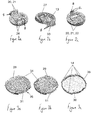
Figures 2a, 2b and 2c are views illustrating a moulded interconnect device located, in use, between an inertial measurement unit and a GPS receiver of the system ofFigure 1 , from different angles; -
Figures 3a, 3b and 3c are views illustrating a second moulded interconnect device located, in use, between the GPS receiver and a processor of the system ofFigure 1 , from different angles; -
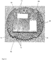
Figure 4 illustrates the inertia! measurement unit connected to the moulded interconnect device; and -
Figure 5 illustrates the GPS receiver, the circuit substrate of which comprises the second moulded interconnect device. - In
Figure 1 , an inertial navigation system is shown, comprising aninertial sensor unit 1, aGPS receiver 2 and aprocessor 3. - The
inertial sensor unit 1 comprises three mutually orthogonal accelerometers and gyroscopes and is assembled from a number of separate circuit boards which slot together. Connections are made between the circuit boards comprising theinertial sensor unit 1 by solder connections between pads of the boards that are adjacent when assembled. The specific form of theinertial sensor unit 1 is not of relevance to the invention and so will not be described in further detail. - A moulded interconnect device 4 (described in greater detail below) is provided between the
inertial sensor unit 1 and theGPS receiver 2. TheGPS receiver 2 includes a circuit substrate (5) which comprises another moulded interconnect device. Moulded interconnect devices may be formed from a moulded part, for example in the form of a plastics material which incorporates a metallic additive that can be activated subsequent to moulding to form conductive metal tracking on the surface of the moulded part. Activation may be achieved by laser activation. An alternative method by which moulded interconnect devices may be formed is by forming a moulded plastics part on which tracks may be formed. For example, the moulded plastics part could be formed from two plastics materials, one of which may be plated to form the tracks. - Moulded non-planar substrates for use as circuit boards are known, and the technology has, for instance, previously been applied to form cellphone antenna which are integrated with a plastics casing of a device. The technology allows conducting tracks to be formed on non-planar surfaces of a plastics material moulded part with a considerable degree of design freedom. Although moulded interconnects forming complex non-planar substrates are known, the use of a moulded interconnect device to both provide mechanical spacing and to make electrical connections using integral conducting tracks between stacked circuit substrates is a new approach in high density packaging.
- The moulded
interconnect device 4 between theinertial sensor unit 1 and theGPS receiver 2 is shown in more detail inFigure 2a to 2c , and comprises ashoulder feature 13, integral mountinglegs 8 upon some of which are provided alignment features 8a,alignment slots 26, throughconnections 27 and conductive tracking 20, 21, 22.Figures 2a and 2c show themoulded interconnect 4 from the side adjacent to theGPS receiver 2, andFigure 2b shows theinterconnect 4 from the side adjacent to theinertial sensor unit 1. - The moulded
interconnect device 4 provides support for theinertial sensor unit 1, and provides electrical connections between theinertial sensor unit 1 and theGPS receiver 2. Conductive metal tracking 20, 21, 22 is formed, in this case, primarily on the surface of theinterconnect device 4 remote from theinertial sensor unit 1, and comprises generallyplanar tracks 20, slopingtracks 21 extending over parts of some of thelegs 8, andsolderable metallisation 22, again provided on some of thelegs 8. An array of electrical connections are made to thelower circuit board 32 of theinertial sensor unit 1 by the connection features 27. The connection features 27 are disposed around the edges of a through hole in the mouldedinterconnect device 4, and comprise sloping features which end adjacent to thelower circuit board 32 of theinertial sensor unit 1 when assembled. - The through hole is substantially rectangular, and the connection features 27 are arranged protruding from the two long sides of the through hole. The connection features 27 comprise further metal tracks provided on a sloping feature of the connection features 27, and solderable metallisation at the tip of the
features 27, adjacent to theinertial sensor 1 when assembled. The slope of the sloping feature of theconnections 27 is substantially 45 degrees, and the sidewalls of the through hole are sloped more steeply than 45 degrees or are substantially vertical. - The connection features 27 may be electrically connected to the
inertial sensor unit 1 by soldering between the solderable metallisation and corresponding solderable metal pads on thelower circuit board 32 of theinertial sensor unit 1. The tips of the connection features 27 are chamfered to create an edge which, when assembled, makes contact substantially in the centre of the corresponding solderable metal pad. It will be appreciated that any suitable soldering technique may be used. - Further connection features 33 are provided at the edge of the moulded interconnect device, comprising some of
legs 8, in this case of sloping form, provided with metal tracking 21, andsolderable metallisation 22. Thefeatures 33 are arranged to extend to the surface of the GPS receiver when assembled. Solder connections may subsequently be made between the connection features 33 and correspondingsolderable pads 28 on theGPS receiver 2. The solder connections may be achieved using any suitable soldering technique. For example, a wave or flow soldering technique may be used, if desired.Tracking 20 extends between the connection features 27 and respective connection features 33, thereby connecting solder pads of theinertial sensor unit 1 withcorresponding solder pads 28 of thecircuit substrate 5 of theGPS receiver 2 when assembled. - The
shoulder feature 13 provides support for theinertial sensor unit 1 when assembled, and corresponds with thelower circuit board 32 thereof. When assembled, thelower circuit board 32 sits within the lip defined by theshoulder feature 13.Slots 26 are further provided which assist in properly aligning theinertial sensor unit 1 with the mouldedinterconnect 4. As the skilled person will appreciate, the proper alignment of theinertial sensor unit 1 relative to the body of the object in which it is installed is important in achieving the highest level of accuracy in navigation and in minimising calibration operations. The provision ofslots 26 and theshoulder feature 13 ensure that the reference alignment between theinertial sensor unit 1 and the mouldedinterconnect device 4 is maintained without the requirement for any jigs or complex assembly arrangements. The mouldedinterconnect 4 is aligned with theGPS receiver 2 by two pegs 8a which mate with corresponding throughholes 31 in thecircuit substrate 5 of theGPS receiver 2. The pegs 8a extend from a face of one of thelegs 8 which extends from the planar surface of the mouldedinterconnect device 4 to thecircuit substrate 5 of theGPS receiver 2 when assembled. When assembled, mechanical contact is made between the planar surface of thecircuit substrate 5 of theGPS receiver 2 and the connection features 33 and face of theleg 8 which carries the pegs 8a. The alignment and the gap between themoulded interconnect 4,inertial sensor unit 1 and theGPS receiver 2 is thereby maintained. - The
legs 8 of the mouldedinterconnect device 4 replace mechanical spacers, pin headers and flex-connectors which would otherwise be necessary to provide mechanical registration and support and to make electrical connections between theinertial sensor unit 1 and theGPS receiver 2. This saves on both the cost of these parts, improves the ease of assembly and provides improved mechanical alignment between theinertial sensor unit 1 and the other components of the inertial navigation system. The invention thus provides an arrangement of relatively simple and convenient form, enabling high density packaging of components, and providing a good mechanical mounting of one substrate upon another whilst also providing the required electrical connections therebetween. - The
GPS receiver 2 comprises acircuit substrate 5 on which is carried aGPS receiver module 10 and a number of other passive components. The GPS receiver module may be a high rate, high precision GPS module capable of very fast acquisition and operation with low signal strength. Thecircuit substrate 5 comprises a substantially planar first side (shown inFigures 3a and 3b ), on which theGPS receiver module 10 and a number of associated electrical components are carried, and a second side (shown inFigure 3c ) on which anelectromagnetic shield 30 is disposed. A connector for thefeed 12 from the GPS antenna (not shown) is further provided. - The
circuit substrate 5 comprises a moulded interconnect device which is provided with connection features 11 (similar to the connection features 33 of the moulded interconnect device between theinertial sensor unit 1 and the GPS receiver 2) which carry electrical connections directly from thesolderable pads 28 through the thickness of thecircuit substrate 5 to the underlyingprocessor circuit board 6. - The planar surface of the
GPS circuit substrate 5 is compatible with standard surface mount technologies. It may thereby be screen printed with solder, populated with electronic components and the solder reflowed in the manner known to the skilled person. - The
GPS receiver module 10 is sensitive to radio frequency interference, and anelectromagnetic shield 30 is therefore provided on the second side of thecircuit substrate 5. Theelectromagnetic shield 30 comprises a conducting planar layer which extends to cover substantially the whole of thecircuit substrate 5, with the exception of the electrical throughconnections circumferential lip 36 which protrudes axially. An electrical connection may be provided to electrically ground theelectromagnetic shield 30. -
Solderable pads 29 are provided on the first side ofcircuit substrate 5 by which theGPS receiver module 10 may be electrically connected to thesubstrate 5. Conductive tracking 34 is provided on thecircuit substrate 5 and arranged to make electrical connections between theGPS receiver module 10, the associated electrical components carried on thesubstrate 5, theGPS antenna feed 12 and the connection features 35. The connection features 35 carry the connections from the first side to the second side of thesubstrate 5. - A
circumferential lip 36 which protrudes axially is provided on the second side of thesubstrate 5 around the perimeter of theelectromagnetic shield 30. Thelip 36 defines the gap between the surface of thecircuit substrate 6 of theprocessor 3 and theelectromagnetic shield 30. The gap thereby provided may accommodate electrical components disposed on the facing side of theprocessor substrate 6 when assembled. Alignment features 14 that protrude both radially and axially are provided on thelip 36 which cooperate withcorresponding recesses 7 of theprocessor substrate 6 and with features of the packaging (not shown) in which the inertial navigation unit may be packaged. - The
processor substrate 6 may comprise a high speed digital processor. The processor may implement algorithms that provide position estimates based on the combined GPS and inertial sensor data. Kalman filters, for instance to minimise error, may be implemented by theprocessor 3, as are known to the skilled person. Theprocessor substrate 6 may be populated with electrical components on either side, or both. Further electrical components may be provided on theprocessor substrate 6, for example for power supply and communication. - The processor and
GPS substrates Figure 1 , the components of the inertial navigation system conform to a circular external profile which, when assembled, tapers from theprocessor 3 to theinertial sensor unit 1. A GPS antenna may be provided at the tip of the narrow end of the stack. Alternative arrangements of inertial navigation system with a different external profile may be more suitable, depending on the application. Such alternative arrangements are contemplated by the inventors as within the scope of the invention. - Although the embodiment described hereinbefore has described an arrangement in which the processor is carried on a separate circuit substrate, an arrangement in which all or part of one or more of the inertial sensor unit, GPS receiver and processor are carried on the same circuit substrate is contemplated as within the scope of the invention.
- As is clear from the forgoing description, the use of moulded interconnect devices in an inertial navigation system helps eliminate many parts that would otherwise be needed, thereby saving cost, volume and mass. The use of such technology enables a design with very high density packaging suitable for applications which are highly constrained by volume or mass.
- Although the foregoing has used a navigation unit as an example of an electronic device that requires high density packaging and is further subject to a range of specific challenges (robustness, accuracy in assembly etc), the invention is not so limited. Electronic devices according to the invention may for example comprise mobile phones, medical devices and miniature persona! computers (e.g. tablets). It will be understood, therefore, that a wide range of modifications and alterations may be made to the arrangement described hereinbefore without departing from the scope of the invention as defined by the claims.
Claims (7)
- An electronic device comprising a circuit substrate (5) configured to carry a GPS receiver module (10) and/or a processor (3), and a moulded interconnect device (4) configured to carry a navigation unit which includes an inertial sensor unit (1), the moulded interconnect device (4) being moulded from a plastics material and incorporating integral legs (8) to mount the interconnect device (4) upon the substrate (5), the legs (8) spacing at least part of the interconnect device (4) from the substrate (5), at least one of the legs (8) carrying a conducting track to provide an electrical interconnection between the interconnect device (4) and the substrate (5), wherein the conducting track is formed integrally with the interconnect device (4), and wherein the conducting track comprises a sloping track (21) extending over part of the at least one of the legs (8).
- The electronic device of Claim 1, wherein the moulded interconnect device (4) further comprises alignment features to ensure correct alignment between the interconnect device (4) and the circuit substrate (5).
- The electronic device of Claim 2, wherein the alignment features comprise protrusions and/or recesses or through holes.
- The electronic device of any of the preceding claims, further comprising an electromagnetic shield (30) carried by the second interconnect device.
- The electronic device of any of the preceding claims, wherein the substrate (5) comprises a second moulded interconnect device.
- The electronic device of claim 5, wherein the second moulded interconnect device is moulded from a plastics material.
- The electronic device of any preceding claim, wherein the plastics material includes a metal additive, activation of which, after moulding, results in the formation of conductive metal tracking on the surface of the moulded interconnect device.
Applications Claiming Priority (2)
| Application Number | Priority Date | Filing Date | Title |
|---|---|---|---|
| GBGB1120981.4A GB201120981D0 (en) | 2011-12-07 | 2011-12-07 | Electronic device |
| PCT/GB2012/052944 WO2013083959A1 (en) | 2011-12-07 | 2012-11-29 | Electronic device comprising a moulded interconnect device |
Publications (2)
| Publication Number | Publication Date |
|---|---|
| EP2788720A1 EP2788720A1 (en) | 2014-10-15 |
| EP2788720B1 true EP2788720B1 (en) | 2020-03-18 |
Family
ID=45541301
Family Applications (1)
| Application Number | Title | Priority Date | Filing Date |
|---|---|---|---|
| EP12808866.3A Active EP2788720B1 (en) | 2011-12-07 | 2012-11-29 | Electronic device comprising a moulded interconnect device |
Country Status (4)
| Country | Link |
|---|---|
| US (1) | US9470530B2 (en) |
| EP (1) | EP2788720B1 (en) |
| GB (1) | GB201120981D0 (en) |
| WO (1) | WO2013083959A1 (en) |
Families Citing this family (5)
| Publication number | Priority date | Publication date | Assignee | Title |
|---|---|---|---|---|
| GB201120981D0 (en) * | 2011-12-07 | 2012-01-18 | Atlantic Inertial Systems Ltd | Electronic device |
| WO2014111210A1 (en) * | 2013-01-18 | 2014-07-24 | Eta Sa Manufacture Horlogère Suisse | Support for a timepiece sensor |
| CN103851596B (en) * | 2014-02-28 | 2016-02-03 | 捷普科技(上海)有限公司 | lamp assembly |
| GB2536037A (en) | 2015-03-05 | 2016-09-07 | Atlantic Inertial Systems Ltd | Anti-vibration mounting system |
| US20210066827A1 (en) | 2019-08-26 | 2021-03-04 | Lockheed Martin Corporation | Pin side edge mount connector and systems and methods thereof |
Citations (2)
| Publication number | Priority date | Publication date | Assignee | Title |
|---|---|---|---|---|
| US20070077747A1 (en) * | 2005-09-30 | 2007-04-05 | John Heck | Microelectronic package having multiple conductive paths through an opening in a support substrate |
| US20110083889A1 (en) * | 2007-06-25 | 2011-04-14 | Molex Incorporated | FPC-Based Relay Connector |
Family Cites Families (15)
| Publication number | Priority date | Publication date | Assignee | Title |
|---|---|---|---|---|
| US3605075A (en) * | 1968-07-01 | 1971-09-14 | Martin Alex Stofkooper | Modular electrical system |
| US4718854A (en) | 1986-12-18 | 1988-01-12 | Amp Incorporated | Low profile press fit connector |
| JPS6435879A (en) * | 1987-07-31 | 1989-02-06 | Texas Instruments Japan | Socket |
| JPH01217993A (en) * | 1988-02-26 | 1989-08-31 | Hitachi Ltd | Semiconductor device |
| US5002493A (en) * | 1989-09-19 | 1991-03-26 | Amp Incorporated | Panel mounted electronic assembly |
| GB2274356A (en) | 1993-04-30 | 1994-07-20 | Itt Ind Ltd | Improvements relating to electrical component mounting arrangements |
| US5831832A (en) * | 1997-08-11 | 1998-11-03 | Motorola, Inc. | Molded plastic ball grid array package |
| US6618011B2 (en) | 2000-10-13 | 2003-09-09 | Nokia Corporation | Antenna transducer assembly, and an associated method therefor |
| US6925413B2 (en) * | 2001-12-14 | 2005-08-02 | Robert Bosch Gmbh | Method and system for detecting a spatial movement state of moving objects |
| JP3956920B2 (en) * | 2003-08-26 | 2007-08-08 | 松下電工株式会社 | connector |
| JP4720827B2 (en) * | 2005-07-11 | 2011-07-13 | パナソニック株式会社 | Board connection member and connection structure |
| JP5108710B2 (en) | 2008-09-30 | 2012-12-26 | モレックス インコーポレイテド | Electrical connector |
| JP5826620B2 (en) * | 2011-11-30 | 2015-12-02 | 日本航空電子工業株式会社 | connector |
| GB201120981D0 (en) * | 2011-12-07 | 2012-01-18 | Atlantic Inertial Systems Ltd | Electronic device |
| JP5871729B2 (en) * | 2012-06-28 | 2016-03-01 | 日本航空電子工業株式会社 | Housingless connector |
-
2011
- 2011-12-07 GB GBGB1120981.4A patent/GB201120981D0/en not_active Ceased
-
2012
- 2012-11-29 US US14/362,214 patent/US9470530B2/en active Active
- 2012-11-29 WO PCT/GB2012/052944 patent/WO2013083959A1/en not_active Ceased
- 2012-11-29 EP EP12808866.3A patent/EP2788720B1/en active Active
Patent Citations (2)
| Publication number | Priority date | Publication date | Assignee | Title |
|---|---|---|---|---|
| US20070077747A1 (en) * | 2005-09-30 | 2007-04-05 | John Heck | Microelectronic package having multiple conductive paths through an opening in a support substrate |
| US20110083889A1 (en) * | 2007-06-25 | 2011-04-14 | Molex Incorporated | FPC-Based Relay Connector |
Non-Patent Citations (1)
| Title |
|---|
| JURGEN GAUSEMEIER ET AL: "Miniature robot BeBot: Mechatronic test platform for self-x properties", INDUSTRIAL INFORMATICS (INDIN), 2011 9TH IEEE INTERNATIONAL CONFERENCE ON, IEEE, 26 July 2011 (2011-07-26), pages 451 - 456, XP031972759, ISBN: 978-1-4577-0435-2, DOI: 10.1109/INDIN.2011.6034921 * |
Also Published As
| Publication number | Publication date |
|---|---|
| EP2788720A1 (en) | 2014-10-15 |
| WO2013083959A1 (en) | 2013-06-13 |
| US20140336930A1 (en) | 2014-11-13 |
| GB201120981D0 (en) | 2012-01-18 |
| US9470530B2 (en) | 2016-10-18 |
Similar Documents
| Publication | Publication Date | Title |
|---|---|---|
| US9470530B2 (en) | Electronic device comprising a moulded interconnect device | |
| CN109839516B (en) | Physical quantity sensor, inertia measurement device, electronic apparatus, and moving object | |
| US8037754B2 (en) | Integrated inertial measurement system and methods of constructing the same | |
| US20230251282A1 (en) | Sensor Module, Measurement System, And Vehicle | |
| CN110346603B (en) | Physical quantity sensor and device, compound sensor device, and electronic device | |
| US20130317741A1 (en) | System on a chip inertial navigation system | |
| CN103449352A (en) | Electronic device, electronic apparatus, and method of manufacturing electronic device | |
| CN109387190B (en) | Physical quantity sensor, inertial measurement unit, electronic device, and moving object | |
| CN110082565B (en) | Physical quantity sensor, electronic apparatus, and moving object | |
| CN107526092B (en) | A miniature autonomous space-time determination unit for satellites | |
| US11282808B2 (en) | Inertial sensor, electronic instrument, vehicle, and method for manufacturing inertial sensor | |
| US10969224B2 (en) | Physical quantity sensor, physical quantity sensor device, composite sensor device, inertia measurement device, vehicle positioning device, portable electronic device, electronic apparatus, vehicle, and output signal adjustment method of physical quantity sensor | |
| JP2019066256A (en) | Physical quantity sensor, inertial measurement device, mobile object positioning device, portable electronic device, electronic device and mobile object | |
| RU2263282C1 (en) | Micro-mechanical sensitive elements-based universal navigation device for controlling motion and unified integrated platform-free inertial navigation system for the device | |
| EP1880422A1 (en) | A device comprising a sensor module | |
| US11084712B2 (en) | Physical quantity sensor with spring having protective beam | |
| JP2019078607A (en) | Physical quantity sensor, inertia measuring device, moving object positioning device, portable electronic apparatus, electronic apparatus, and moving object | |
| JP4404225B2 (en) | Antenna device | |
| CN109668554A (en) | Physical quantity transducer, inertial measuring unit, electronic equipment and moving body | |
| US8978474B2 (en) | Inertial measurement systems, and methods of use and manufacture thereof | |
| CN109682993A (en) | Physical quantity transducer, electronic equipment and moving body | |
| CN111735990B (en) | Inertial sensor, electronic apparatus, and moving object | |
| JP6987683B2 (en) | Communication device, control method of communication device, and control program of communication device | |
| CN113148942A (en) | External packaging structure, MEMS sensor and electronic equipment | |
| US10386204B2 (en) | Integrated sensor and homologous calibration structure for resonant devices |
Legal Events
| Date | Code | Title | Description |
|---|---|---|---|
| PUAI | Public reference made under article 153(3) epc to a published international application that has entered the european phase |
Free format text: ORIGINAL CODE: 0009012 |
|
| 17P | Request for examination filed |
Effective date: 20140618 |
|
| AK | Designated contracting states |
Kind code of ref document: A1 Designated state(s): AL AT BE BG CH CY CZ DE DK EE ES FI FR GB GR HR HU IE IS IT LI LT LU LV MC MK MT NL NO PL PT RO RS SE SI SK SM TR |
|
| DAX | Request for extension of the european patent (deleted) | ||
| STAA | Information on the status of an ep patent application or granted ep patent |
Free format text: STATUS: EXAMINATION IS IN PROGRESS |
|
| 17Q | First examination report despatched |
Effective date: 20170428 |
|
| RIC1 | Information provided on ipc code assigned before grant |
Ipc: H05K 1/14 20060101ALI20190802BHEP Ipc: G01S 19/13 20100101ALI20190802BHEP Ipc: G01C 21/16 20060101AFI20190802BHEP Ipc: G01S 19/49 20100101ALI20190802BHEP Ipc: G01S 19/35 20100101ALI20190802BHEP Ipc: H05K 1/11 20060101ALI20190802BHEP |
|
| GRAP | Despatch of communication of intention to grant a patent |
Free format text: ORIGINAL CODE: EPIDOSNIGR1 |
|
| STAA | Information on the status of an ep patent application or granted ep patent |
Free format text: STATUS: GRANT OF PATENT IS INTENDED |
|
| RIN1 | Information on inventor provided before grant (corrected) |
Inventor name: THOMAS, HENRY |
|
| INTG | Intention to grant announced |
Effective date: 20190925 |
|
| GRAS | Grant fee paid |
Free format text: ORIGINAL CODE: EPIDOSNIGR3 |
|
| GRAA | (expected) grant |
Free format text: ORIGINAL CODE: 0009210 |
|
| STAA | Information on the status of an ep patent application or granted ep patent |
Free format text: STATUS: THE PATENT HAS BEEN GRANTED |
|
| AK | Designated contracting states |
Kind code of ref document: B1 Designated state(s): AL AT BE BG CH CY CZ DE DK EE ES FI FR GB GR HR HU IE IS IT LI LT LU LV MC MK MT NL NO PL PT RO RS SE SI SK SM TR |
|
| REG | Reference to a national code |
Ref country code: GB Ref legal event code: FG4D |
|
| REG | Reference to a national code |
Ref country code: DE Ref legal event code: R096 Ref document number: 602012068604 Country of ref document: DE |
|
| REG | Reference to a national code |
Ref country code: AT Ref legal event code: REF Ref document number: 1246407 Country of ref document: AT Kind code of ref document: T Effective date: 20200415 Ref country code: IE Ref legal event code: FG4D |
|
| PG25 | Lapsed in a contracting state [announced via postgrant information from national office to epo] |
Ref country code: RS Free format text: LAPSE BECAUSE OF FAILURE TO SUBMIT A TRANSLATION OF THE DESCRIPTION OR TO PAY THE FEE WITHIN THE PRESCRIBED TIME-LIMIT Effective date: 20200318 Ref country code: FI Free format text: LAPSE BECAUSE OF FAILURE TO SUBMIT A TRANSLATION OF THE DESCRIPTION OR TO PAY THE FEE WITHIN THE PRESCRIBED TIME-LIMIT Effective date: 20200318 Ref country code: NO Free format text: LAPSE BECAUSE OF FAILURE TO SUBMIT A TRANSLATION OF THE DESCRIPTION OR TO PAY THE FEE WITHIN THE PRESCRIBED TIME-LIMIT Effective date: 20200618 |
|
| REG | Reference to a national code |
Ref country code: NL Ref legal event code: MP Effective date: 20200318 |
|
| PG25 | Lapsed in a contracting state [announced via postgrant information from national office to epo] |
Ref country code: BG Free format text: LAPSE BECAUSE OF FAILURE TO SUBMIT A TRANSLATION OF THE DESCRIPTION OR TO PAY THE FEE WITHIN THE PRESCRIBED TIME-LIMIT Effective date: 20200618 Ref country code: LV Free format text: LAPSE BECAUSE OF FAILURE TO SUBMIT A TRANSLATION OF THE DESCRIPTION OR TO PAY THE FEE WITHIN THE PRESCRIBED TIME-LIMIT Effective date: 20200318 Ref country code: SE Free format text: LAPSE BECAUSE OF FAILURE TO SUBMIT A TRANSLATION OF THE DESCRIPTION OR TO PAY THE FEE WITHIN THE PRESCRIBED TIME-LIMIT Effective date: 20200318 Ref country code: HR Free format text: LAPSE BECAUSE OF FAILURE TO SUBMIT A TRANSLATION OF THE DESCRIPTION OR TO PAY THE FEE WITHIN THE PRESCRIBED TIME-LIMIT Effective date: 20200318 Ref country code: GR Free format text: LAPSE BECAUSE OF FAILURE TO SUBMIT A TRANSLATION OF THE DESCRIPTION OR TO PAY THE FEE WITHIN THE PRESCRIBED TIME-LIMIT Effective date: 20200619 |
|
| REG | Reference to a national code |
Ref country code: LT Ref legal event code: MG4D |
|
| PG25 | Lapsed in a contracting state [announced via postgrant information from national office to epo] |
Ref country code: NL Free format text: LAPSE BECAUSE OF FAILURE TO SUBMIT A TRANSLATION OF THE DESCRIPTION OR TO PAY THE FEE WITHIN THE PRESCRIBED TIME-LIMIT Effective date: 20200318 |
|
| PG25 | Lapsed in a contracting state [announced via postgrant information from national office to epo] |
Ref country code: PT Free format text: LAPSE BECAUSE OF FAILURE TO SUBMIT A TRANSLATION OF THE DESCRIPTION OR TO PAY THE FEE WITHIN THE PRESCRIBED TIME-LIMIT Effective date: 20200812 Ref country code: EE Free format text: LAPSE BECAUSE OF FAILURE TO SUBMIT A TRANSLATION OF THE DESCRIPTION OR TO PAY THE FEE WITHIN THE PRESCRIBED TIME-LIMIT Effective date: 20200318 Ref country code: SM Free format text: LAPSE BECAUSE OF FAILURE TO SUBMIT A TRANSLATION OF THE DESCRIPTION OR TO PAY THE FEE WITHIN THE PRESCRIBED TIME-LIMIT Effective date: 20200318 Ref country code: RO Free format text: LAPSE BECAUSE OF FAILURE TO SUBMIT A TRANSLATION OF THE DESCRIPTION OR TO PAY THE FEE WITHIN THE PRESCRIBED TIME-LIMIT Effective date: 20200318 Ref country code: SK Free format text: LAPSE BECAUSE OF FAILURE TO SUBMIT A TRANSLATION OF THE DESCRIPTION OR TO PAY THE FEE WITHIN THE PRESCRIBED TIME-LIMIT Effective date: 20200318 Ref country code: IS Free format text: LAPSE BECAUSE OF FAILURE TO SUBMIT A TRANSLATION OF THE DESCRIPTION OR TO PAY THE FEE WITHIN THE PRESCRIBED TIME-LIMIT Effective date: 20200718 Ref country code: CZ Free format text: LAPSE BECAUSE OF FAILURE TO SUBMIT A TRANSLATION OF THE DESCRIPTION OR TO PAY THE FEE WITHIN THE PRESCRIBED TIME-LIMIT Effective date: 20200318 Ref country code: LT Free format text: LAPSE BECAUSE OF FAILURE TO SUBMIT A TRANSLATION OF THE DESCRIPTION OR TO PAY THE FEE WITHIN THE PRESCRIBED TIME-LIMIT Effective date: 20200318 |
|
| REG | Reference to a national code |
Ref country code: AT Ref legal event code: MK05 Ref document number: 1246407 Country of ref document: AT Kind code of ref document: T Effective date: 20200318 |
|
| REG | Reference to a national code |
Ref country code: DE Ref legal event code: R097 Ref document number: 602012068604 Country of ref document: DE |
|
| PLBE | No opposition filed within time limit |
Free format text: ORIGINAL CODE: 0009261 |
|
| STAA | Information on the status of an ep patent application or granted ep patent |
Free format text: STATUS: NO OPPOSITION FILED WITHIN TIME LIMIT |
|
| PG25 | Lapsed in a contracting state [announced via postgrant information from national office to epo] |
Ref country code: IT Free format text: LAPSE BECAUSE OF FAILURE TO SUBMIT A TRANSLATION OF THE DESCRIPTION OR TO PAY THE FEE WITHIN THE PRESCRIBED TIME-LIMIT Effective date: 20200318 Ref country code: DK Free format text: LAPSE BECAUSE OF FAILURE TO SUBMIT A TRANSLATION OF THE DESCRIPTION OR TO PAY THE FEE WITHIN THE PRESCRIBED TIME-LIMIT Effective date: 20200318 Ref country code: AT Free format text: LAPSE BECAUSE OF FAILURE TO SUBMIT A TRANSLATION OF THE DESCRIPTION OR TO PAY THE FEE WITHIN THE PRESCRIBED TIME-LIMIT Effective date: 20200318 Ref country code: ES Free format text: LAPSE BECAUSE OF FAILURE TO SUBMIT A TRANSLATION OF THE DESCRIPTION OR TO PAY THE FEE WITHIN THE PRESCRIBED TIME-LIMIT Effective date: 20200318 |
|
| 26N | No opposition filed |
Effective date: 20201221 |
|
| PG25 | Lapsed in a contracting state [announced via postgrant information from national office to epo] |
Ref country code: PL Free format text: LAPSE BECAUSE OF FAILURE TO SUBMIT A TRANSLATION OF THE DESCRIPTION OR TO PAY THE FEE WITHIN THE PRESCRIBED TIME-LIMIT Effective date: 20200318 |
|
| PG25 | Lapsed in a contracting state [announced via postgrant information from national office to epo] |
Ref country code: SI Free format text: LAPSE BECAUSE OF FAILURE TO SUBMIT A TRANSLATION OF THE DESCRIPTION OR TO PAY THE FEE WITHIN THE PRESCRIBED TIME-LIMIT Effective date: 20200318 |
|
| PG25 | Lapsed in a contracting state [announced via postgrant information from national office to epo] |
Ref country code: MC Free format text: LAPSE BECAUSE OF FAILURE TO SUBMIT A TRANSLATION OF THE DESCRIPTION OR TO PAY THE FEE WITHIN THE PRESCRIBED TIME-LIMIT Effective date: 20200318 |
|
| REG | Reference to a national code |
Ref country code: CH Ref legal event code: PL |
|
| PG25 | Lapsed in a contracting state [announced via postgrant information from national office to epo] |
Ref country code: LU Free format text: LAPSE BECAUSE OF NON-PAYMENT OF DUE FEES Effective date: 20201129 |
|
| REG | Reference to a national code |
Ref country code: BE Ref legal event code: MM Effective date: 20201130 |
|
| PG25 | Lapsed in a contracting state [announced via postgrant information from national office to epo] |
Ref country code: CH Free format text: LAPSE BECAUSE OF NON-PAYMENT OF DUE FEES Effective date: 20201130 Ref country code: LI Free format text: LAPSE BECAUSE OF NON-PAYMENT OF DUE FEES Effective date: 20201130 |
|
| REG | Reference to a national code |
Ref country code: IE Ref legal event code: MM4A |
|
| PG25 | Lapsed in a contracting state [announced via postgrant information from national office to epo] |
Ref country code: IE Free format text: LAPSE BECAUSE OF NON-PAYMENT OF DUE FEES Effective date: 20201129 |
|
| PG25 | Lapsed in a contracting state [announced via postgrant information from national office to epo] |
Ref country code: TR Free format text: LAPSE BECAUSE OF FAILURE TO SUBMIT A TRANSLATION OF THE DESCRIPTION OR TO PAY THE FEE WITHIN THE PRESCRIBED TIME-LIMIT Effective date: 20200318 Ref country code: MT Free format text: LAPSE BECAUSE OF FAILURE TO SUBMIT A TRANSLATION OF THE DESCRIPTION OR TO PAY THE FEE WITHIN THE PRESCRIBED TIME-LIMIT Effective date: 20200318 Ref country code: CY Free format text: LAPSE BECAUSE OF FAILURE TO SUBMIT A TRANSLATION OF THE DESCRIPTION OR TO PAY THE FEE WITHIN THE PRESCRIBED TIME-LIMIT Effective date: 20200318 |
|
| PG25 | Lapsed in a contracting state [announced via postgrant information from national office to epo] |
Ref country code: MK Free format text: LAPSE BECAUSE OF FAILURE TO SUBMIT A TRANSLATION OF THE DESCRIPTION OR TO PAY THE FEE WITHIN THE PRESCRIBED TIME-LIMIT Effective date: 20200318 Ref country code: AL Free format text: LAPSE BECAUSE OF FAILURE TO SUBMIT A TRANSLATION OF THE DESCRIPTION OR TO PAY THE FEE WITHIN THE PRESCRIBED TIME-LIMIT Effective date: 20200318 |
|
| PG25 | Lapsed in a contracting state [announced via postgrant information from national office to epo] |
Ref country code: BE Free format text: LAPSE BECAUSE OF NON-PAYMENT OF DUE FEES Effective date: 20201130 |
|
| P01 | Opt-out of the competence of the unified patent court (upc) registered |
Effective date: 20230630 |
|
| PGFP | Annual fee paid to national office [announced via postgrant information from national office to epo] |
Ref country code: DE Payment date: 20251022 Year of fee payment: 14 |
|
| PGFP | Annual fee paid to national office [announced via postgrant information from national office to epo] |
Ref country code: GB Payment date: 20251023 Year of fee payment: 14 |
|
| PGFP | Annual fee paid to national office [announced via postgrant information from national office to epo] |
Ref country code: FR Payment date: 20251022 Year of fee payment: 14 |