EP2787595A2 - Non-contact communication coil, non-contact power feeding device, and non-contact power receiving device - Google Patents
Non-contact communication coil, non-contact power feeding device, and non-contact power receiving device Download PDFInfo
- Publication number
- EP2787595A2 EP2787595A2 EP14162909.7A EP14162909A EP2787595A2 EP 2787595 A2 EP2787595 A2 EP 2787595A2 EP 14162909 A EP14162909 A EP 14162909A EP 2787595 A2 EP2787595 A2 EP 2787595A2
- Authority
- EP
- European Patent Office
- Prior art keywords
- coil
- receiver
- power
- power receiving
- resonance
- Prior art date
- Legal status (The legal status is an assumption and is not a legal conclusion. Google has not performed a legal analysis and makes no representation as to the accuracy of the status listed.)
- Granted
Links
Images


Classifications
-
- H—ELECTRICITY
- H01—ELECTRIC ELEMENTS
- H01F—MAGNETS; INDUCTANCES; TRANSFORMERS; SELECTION OF MATERIALS FOR THEIR MAGNETIC PROPERTIES
- H01F38/00—Adaptations of transformers or inductances for specific applications or functions
- H01F38/14—Inductive couplings
-
- H—ELECTRICITY
- H01—ELECTRIC ELEMENTS
- H01F—MAGNETS; INDUCTANCES; TRANSFORMERS; SELECTION OF MATERIALS FOR THEIR MAGNETIC PROPERTIES
- H01F27/00—Details of transformers or inductances, in general
- H01F27/006—Details of transformers or inductances, in general with special arrangement or spacing of turns of the winding(s), e.g. to produce desired self-resonance
-
- H—ELECTRICITY
- H02—GENERATION; CONVERSION OR DISTRIBUTION OF ELECTRIC POWER
- H02J—ELECTRIC POWER NETWORKS; CIRCUIT ARRANGEMENTS OR SYSTEMS FOR SUPPLYING OR DISTRIBUTING ELECTRIC POWER; SYSTEMS FOR STORING ELECTRIC ENERGY
- H02J50/00—Circuit arrangements or systems for wireless supply or distribution of electric power
- H02J50/10—Circuit arrangements or systems for wireless supply or distribution of electric power using inductive coupling
- H02J50/12—Circuit arrangements or systems for wireless supply or distribution of electric power using inductive coupling of the resonant type
Definitions
- the present invention relates to a non-contact communication coil.
- Patent Document 1 a non-contact communication medium that is provided with a power receiving coil and a data receiving coil and that connects a cancellation coil substantially having the same inductance as a mutual inductance of the power receiving coil and the data receiving coil to connection points thereof.
- a magnetic field emitted from the power receiving coil thereby cancels an electromotive force, which is noise generated in the data receiving coil, and improves reliability of data reception.
- Patent Document 1 Japanese Unexamined Patent Application Publication No. H4-305789
- the data receiving coil does not have features in particular of its own, and a separate cancellation coil is needed.
- One or more embodiments of the present invention provide a non-contact communication coil having a configuration that can improve performance of data communication.
- an induction voltage induced in the non-contact communication coil by the current that passes through the other coil can be suppressed. Therefore, for example, performance of data communication can be improved by suppressing effects from the other coil.
- the first receiver may be configured by winding a coil extending in a longitudinal direction around an axis perpendicular to the longitudinal direction so the longitudinal direction becomes a circumferential direction, and the second receiver is a coil wound in the circumferential direction.
- the power transmission coil, power receiving coil, and the resonance coil may be arranged nearer to the first receiver than to the second receiver.
- central axes of the first receiver and the second receiver may be coaxial. A communication area relative to an outermost shape size of the non-contact communication coil can thereby be widened.
- outer shape sizes of the first receiver and the second receiver may be identical.
- the communication area relative to the outermost shape size of the non-contact communication coil can thereby be widened.
- a non-contact power feeding device may comprise any of the above non-contact communication coils, wherein the power transmission coil is joined with the resonance coil.
- the induction voltage induced in the non-contact communication coil by the current that passes through the power transmission coil and the resonance coil can be suppressed, and data communication reliability can be improved by suppressing an effect from these coils.
- a non-contact power feeding device may comprise any of the above non-contact communication coils, wherein the power transmission coil is shared with the resonance coil.
- the induction voltage induced in the non-contact communication coil by the current that passes through the power transmission coil shared with the resonance coil can be suppressed, and data communication reliability can be improved by suppressing an effect from the power transmission coil.
- a non-contact power feeding device may comprise any of the above non-contact communication coils, wherein the power receiving coil is joined with the resonance coil.
- an induction voltage induced in the non-contact communication coil by a current that passes through the power receiving coil and the resonance coil can be suppressed, and data communication reliability can be improved by suppressing an effect from these coils.
- the performance of data communication can be improved by suppressing the effect from the other coil.
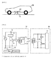
- FIG. 1 An example where a power feeding device and a power receiving device according to one or more embodiments of a first example of the present invention are applied in charging an electric vehicle is illustrated in FIG. 1 .
- a power feeding device 10 is disposed on a ground surface of a location where an electric vehicle 25 parks, and a power receiving device 20 is disposed on a bottom surface of the electric vehicle 25.
- the power feeding device 10 emits a magnetic field in a state where the power receiving device 20 opposes the power feeding device 10 at or within a predetermined distance, and the power receiving device 20 receives the magnetic field and is fed with power.
- communication occurs between the power feeding device 10 and the power receiving device 20 for notifying a start/end of power feeding, notifying a power feeding condition, exchanging information with each other, and the like.
- FIG. 2 A block diagram illustrating a specific configuration of the power feeding device 10 and the power receiving device 20 is illustrated in FIG. 2 .
- the power feeding device 10 is provide with an oscillator 11, a driver 12, a modulator 13, a communication coil 14, a receiver 15, a controller 16, a power transmission coil L1, a resonance coil L2, and a resonance condenser C1.
- the power receiving device 20 comprises a power receiving coil L3, a resonance condenser C2, a resistance R1, a change-over switch SW1, and a power receiving circuit 21.
- the oscillator 11 generates a high-frequency signal having a frequency of a radiation magnetic field for power transmission.
- the driver 12 amplifies the high-frequency signal generated by the oscillator 11 by switching and passes a current with high frequency to the power transmission coil L1.
- the modulator 13 performs amplitude shift keying (ASK) modulation on the radiation magnetic field by controlling the driver 12 when sending data to the power receiving device 20.
- ASK amplitude shift keying
- the power transmission coil L1 emits a magnetic field for power transmission when a high-frequency current passes therethrough.
- the resonance coil L2 configures the resonance condenser C1 and a resonance circuit.
- the resonance coil L2 receives the magnetic field emitted by the power transmission coil L1 and emits a larger magnetic field for power transmission by passing a resonance current therethrough.
- the communication coil 14 (non-contact communication coil) is a coil for receiving data from the power receiving device 20 and can receive data without being affected by the magnetic field emitted from the power transmission coil L1 and the resonance coil L2. A detailed configuration of the communication coil 14 will be described below.
- the receiver 15 demodulates a signal received at the communication coil 14 for receiving data from the power receiving device 20.
- the controller 16 controls various components of the power feeding device 10, such as the oscillator 11, the driver 12, the modulator 13, and the receiver 15.
- the resonance condenser C2 may be provided in the power receiving device 20 to configure the power receiving coil L3 and the resonance circuit, but the resonance condenser C2 is not needed. Moreover, besides the power receiving coil, a resonance coil may be provided on the power receiving device 20 side, as in the power feeding device 10.
- a control by the modulator 13 modulates the magnetic field emitted from the resonance coil L2. Then, on the power receiving device 20 side, this emitted magnetic field is received by the power receiving coil L3, and the induced electromotive force is generated by the power receiving coil L3.
- the power receiving circuit 21 takes out data from this change in the generated induced electromotive force.
- a load impedance of the power receiving coil L3 is changed by switching the change-over switch SW1 connected to the resistance R1 according to the transmission data and emitting the magnetic field from the power receiving coil L3. Then, on the power feeding device 10 side, this emitted magnetic field is received by the communication coil 14, and the transmitter 15 takes out data by detecting a change in inductive voltage generated by the communication coil 14.
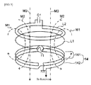
- each coil is illustrated as a line segment for convenience, but each coil of course has thickness in reality.
- the communication coil 14 is configured from a proximal receiver 141 disposed in a position close to the resonance coil L2 and the power transmission coil L1, and a distal receiver 142 disposed in a position far from the resonance coil L2 and the power transmission coil L1.
- the proximal receiver 141 and the distal receiver 142 are connected in series. One end of the proximal receiver 141 is connected to a ground, and one end of the distal receiver 142 is connected to the receiver 15 ( FIG. 2 ).
- the proximal receiver 141 illustrated in FIG. 3 is a winding coil in a U shape with one end open extending in a longitudinal direction and wound once around an axis S orthogonal to the longitudinal direction so that the longitudinal direction becomes a circumferential direction.
- a magnetic flux (for example, a magnetic flux M1 in FIG. 3 ) arising from the current passing through the power transmission coil L1 and the resonance coil L2 interlinks with the proximal receiver 141. That is, the magnetic flux passes through a region P surrounded by the coil illustrated in FIG. 4 .
- the distal receiver 142 illustrated in FIG. 3 is configured from a coil wound once in the circumferential direction of the proximal receiver 141, may have a central axis substantially coaxial to that of the proximal receiver 141, and may have an outer diameter substantially the same as that of the proximal receiver 141.
- a magnetic flux (for example, a magnetic flux M2 in FIG. 3 ) arising from the current passing through the power transmission coil L1 and the resonance coil L2 interlinks with the distal receiver 142.
- a magnetic flux (for example, a magnetic flux M3 illustrated in FIG. 3 ) emitted for data transmission from the power receiving device 20 positioned more distally than the power transmission coil L1 and the resonance coil L2 interlinks with the distal receiver 142.
- an inductive voltage arising in the communication coil 14 is expressed by e1-e2+e3. That is, e1 and -e2 become inductive voltages of mutually opposite directions.
- the magnetic flux emitted from the power receiving device 20 does not interlink with the proximal receiver 141, and the inductive voltage therefore does not arise in the proximal receiver 141 due to the magnetic flux.
- e1 e2; that is, the inductive voltage arising in the distal receiver 142 by interlinking the magnetic flux arising from the current passing through the power transmission coil L1 and the resonance coil L2 and the inductive voltage arising in the proximal receiver 141 by interlinking the magnetic flux arising from the current passing through the power transmission coil L1 and the resonance coil L2 are designed to be equivalent.
- the inductive voltage arising in the communication coil 14 becomes e3, and it becomes possible to take out only the inductive voltage due to the magnetic flux emitted as data from the power receiving device 20. Therefore, reliability of data reception can be increased without being affected by the radiation magnetic field from the power transmission coil L1 and the resonance coil L2.
- a width W in the example in FIG. 4 a width W in the example in FIG. 4
- a winding count of the proximal receiver 141 with the longitudinal direction as the circumferential direction a winding count of the distal receiver 142.
- the winding count of the proximal receiver 141 with the longitudinal direction as the circumferential direction is one time, but the winding count may be a plurality of times.
- FIG. 5 illustrates the proximal receiver 141 where the winding coil wound in the U shape illustrated in FIG. 4 is wound twice with the longitudinal direction as the circumferential direction.
- the example in FIG. 5 comprises a structure forming two layers in a radial direction.
- the winding count of the distal receiver 142 is one time but is not limited thereto and may be a plurality of times. Winding the plurality of times may improve data reception voltage.
- the wiring coil wound in the U shape is used as the proximal receiver 141, but as long as conditions of the inductive voltage described above are met, the proximal receiver 141, as illustrated in FIG. 6 for example, may be configured to wind the winding coil, which is wound around the axis S so an outer shape becomes substantially rectangular, one or more times with the longitudinal direction as the circumferential direction.
- the proximal receiver 141 and the distal receiver 142 may have substantially coaxial central axes, and the outer diameters are also substantially the same (i.e., outer shape sizes are substantially the same). While this condition is not needed, it can increase a size of the distal receiver 142 relative to an outermost shape size of the communication coil 14, that is, a communication area.
- the communication coil 14 is used for data reception, but the communication coil 14 may be used for data transmission. It is thereby possible to perform high-speed data transmission without being affected by the current passing through the power transmission coil L1 and the resonance coil L2.
- power transmission and data reception by the communication coil 14 are assumed to use the same frequency, but effectiveness is the same even when differing frequencies are used.
- FIG. 7 illustrates a configuration of a power feeding device according to one or more embodiments of a second example of the present invention.
- a power feeding device 30 illustrated in FIG. 7 comprises an oscillator 31, a driver 32, a communication coil 33, a communication circuit 34, a controller 35, a resonance condenser C3, and a power transmission coil L4.
- a difference between the present example and the first example ( FIG. 2 ) is that the present example may share the power transmission coil L4 with a resonance coil and that the resonance condenser C3 and the power transmission coil L4 may configure a resonance circuit.
- a magnetic field may be emitted and power transmitted to a power receiving device (not illustrated) by a resonance current passing through the power transmission coil L4.
- data may be sent and received using the communication coil 33 and the communication circuit 34.
- the communication coil 33 may be configured in the same manner as one or more embodiments of the first example, from a proximal receiver disposed in a position close to the power transmission coil L4 and a distal receiver disposed in a position far from the power transmission coil L4 and connected in series with the proximal receiver.
- Values of each induction voltage of an opposite direction generated in the proximal receiver and the distal receiver by interlinking a magnetic flux arising from a current passing through the power transmission coil L4 are designed to be the same. Only the induction voltage generated in the distal receiver by interlinking the magnetic flux emitted as data from the power receiving device (not illustrated) can thereby by taken out. Therefore, reliability of data reception improves without being affected by the current passing through the power transmission coil L4.
- the communication coil 33 when used for data transmission, high-speed data transmission can be performed without being affected by the current passing through the power transmission coil L4.
- FIG. 8 illustrates a configuration of a power receiving device according to one or more embodiments of a third example of the present invention.
- the present example is an example of applying a communication coil to a power receiving device side instead of a power feeding device.
- a power receiving device 40 illustrated in FIG. 8 comprises a communication coil 41, a receiver 42, a power receiving circuit 43, a controller 44, a resonance condenser C4, a resonance coil L5, a power receiving coil L6, a resistance R2, and a change-over switch SW2.
- the resonance coil L5 When a magnetic field for power transmission is emitted from the power feeding device (not illustrated), the resonance coil L5 receives this magnetic field, and a resonance current passes through a resonance circuit configured from the resonance condenser C4 and the resonance coil L5. An induced electromotive force is generated in the power receiving coil L6 joined with the resonance coil L5 by the resonance current, and the induced electromotive force is taken out as power.
- a load impedance of the power receiving coil L6 is changed and data is transmitted by switching the change-over switch SW2 connected to the resistance R2 according to transmission data.
- the communication coil 41 is configured from a proximal receiver disposed in a position close to the power receiving coil L6 and the resonance coil L5 and a distal receiver disposed in a position far from the power receiving coil L6 and the resonance coil L5 and connected in series with the proximal receiver.
- Values of each induction voltage of an opposite direction generated in the proximal receiver and the distal receiver by interlinking a magnetic flux arising from a current passing through the power receiving coil L6 and the resonance coil L5 are designed to be the same. Only the induction voltage generated in the distal receiver by interlinking the magnetic flux emitted as data from the power feeding device (not illustrated) can thereby by taken out. Therefore, reliability of data reception improves without being affected by the current passing through the power receiving coil L6 and the resonance coil L5.
Landscapes
- Engineering & Computer Science (AREA)
- Power Engineering (AREA)
- Computer Networks & Wireless Communication (AREA)
- Near-Field Transmission Systems (AREA)
- Charge And Discharge Circuits For Batteries Or The Like (AREA)
- Current-Collector Devices For Electrically Propelled Vehicles (AREA)
Abstract
Description
- The present invention relates to a non-contact communication coil.
- Conventionally, a device that feeds and receives power in a non-contact method and performs data communication is known.
- For example, in Patent Document 1, a non-contact communication medium that is provided with a power receiving coil and a data receiving coil and that connects a cancellation coil substantially having the same inductance as a mutual inductance of the power receiving coil and the data receiving coil to connection points thereof.
- A magnetic field emitted from the power receiving coil thereby cancels an electromotive force, which is noise generated in the data receiving coil, and improves reliability of data reception.
- [Patent Document 1] Japanese Unexamined Patent Application Publication No.
H4-305789 - However, in a technique of Patent Document 1 described above, the data receiving coil does not have features in particular of its own, and a separate cancellation coil is needed.
- One or more embodiments of the present invention provide a non-contact communication coil having a configuration that can improve performance of data communication.
- According to one or more embodiments, a non-contact communication coil configured to a non-contact power feeding device comprising a power transmission coil, a power receiving coil, and a resonance coil may comprise: a first receiver; and a second receiver connected in series with the first receiver, wherein the non-contact communication coil is configured to generate induction voltages in mutually opposing directions in the first receiver and the second receiver when current passes through at least one of the power transmission coil and the power receiving coil.
- According to such a configuration, for example, an induction voltage induced in the non-contact communication coil by the current that passes through the other coil can be suppressed. Therefore, for example, performance of data communication can be improved by suppressing effects from the other coil.
- For example, in one or more embodiments, the first receiver may be configured by winding a coil extending in a longitudinal direction around an axis perpendicular to the longitudinal direction so the longitudinal direction becomes a circumferential direction, and the second receiver is a coil wound in the circumferential direction.
- For example, in one or more embodiments, the power transmission coil, power receiving coil, and the resonance coil may be arranged nearer to the first receiver than to the second receiver.
- Furthermore, in one or more embodiments, central axes of the first receiver and the second receiver may be coaxial. A communication area relative to an outermost shape size of the non-contact communication coil can thereby be widened.
- Furthermore, in one or more embodiments, outer shape sizes of the first receiver and the second receiver may be identical. The communication area relative to the outermost shape size of the non-contact communication coil can thereby be widened.
- Furthermore, a non-contact power feeding device according to one or more embodiments may comprise any of the above non-contact communication coils, wherein the power transmission coil is joined with the resonance coil.
- According to such a configuration, for example, the induction voltage induced in the non-contact communication coil by the current that passes through the power transmission coil and the resonance coil can be suppressed, and data communication reliability can be improved by suppressing an effect from these coils.
- Furthermore, a non-contact power feeding device according to one or more embodiments may comprise any of the above non-contact communication coils, wherein the power transmission coil is shared with the resonance coil.
- According to such a configuration, the induction voltage induced in the non-contact communication coil by the current that passes through the power transmission coil shared with the resonance coil can be suppressed, and data communication reliability can be improved by suppressing an effect from the power transmission coil.
- Furthermore, a non-contact power feeding device according to one or more embodiments may comprise any of the above non-contact communication coils, wherein the power receiving coil is joined with the resonance coil.
- According to such a configuration, for example, an induction voltage induced in the non-contact communication coil by a current that passes through the power receiving coil and the resonance coil can be suppressed, and data communication reliability can be improved by suppressing an effect from these coils.
- According to the non-contact communication coil of one or more embodiments of the present invention, the performance of data communication can be improved by suppressing the effect from the other coil.
-
-
FIG. 1 is a schematic diagram of a charging system of an electric vehicle according to one or more embodiments of a first example of the present invention. -
FIG. 2 is a block diagram of a power feeding/receiving device according to one or more embodiments of the first example of the present invention. -
FIG. 3 is a diagram illustrating a configuration example of a communication coil according to one or more embodiments of the first example of the present invention. -
FIG. 4 is a development view (plan view) illustrating an example of a proximal receiver according to one or more embodiments of the first example of the present invention. -
FIG. 5 is a diagram illustrating another configuration example of the proximal receiver according to one or more embodiments of the first example of the present invention. -
FIG. 6 is a development view (plan view) illustrating an example of the proximal receiver according to one or more embodiments of the first example of the present invention. -
FIG. 7 is a block diagram of a power feeding device according to one or more embodiments of a second example of the present invention. -
FIG. 8 is a block diagram of a power receiving device according to one or more embodiments of the third example of the present invention. - Embodiments of the present invention will be described below with reference to drawings. An example where a power feeding device and a power receiving device according to one or more embodiments of a first example of the present invention are applied in charging an electric vehicle is illustrated in
FIG. 1 . - In one or more embodiments, as illustrated by way of example in
FIG. 1 , at a charging stand or in a parking lot or the like, apower feeding device 10 is disposed on a ground surface of a location where anelectric vehicle 25 parks, and apower receiving device 20 is disposed on a bottom surface of theelectric vehicle 25. Thepower feeding device 10 emits a magnetic field in a state where thepower receiving device 20 opposes thepower feeding device 10 at or within a predetermined distance, and thepower receiving device 20 receives the magnetic field and is fed with power. Moreover, communication occurs between thepower feeding device 10 and thepower receiving device 20 for notifying a start/end of power feeding, notifying a power feeding condition, exchanging information with each other, and the like. - A block diagram illustrating a specific configuration of the
power feeding device 10 and thepower receiving device 20 is illustrated inFIG. 2 . As illustrated inFIG. 2 , thepower feeding device 10 is provide with anoscillator 11, adriver 12, amodulator 13, acommunication coil 14, areceiver 15, acontroller 16, a power transmission coil L1, a resonance coil L2, and a resonance condenser C1. Moreover, the power receivingdevice 20 comprises a power receiving coil L3, a resonance condenser C2, a resistance R1, a change-over switch SW1, and apower receiving circuit 21. - The
oscillator 11 generates a high-frequency signal having a frequency of a radiation magnetic field for power transmission. Thedriver 12 amplifies the high-frequency signal generated by theoscillator 11 by switching and passes a current with high frequency to the power transmission coil L1. Themodulator 13 performs amplitude shift keying (ASK) modulation on the radiation magnetic field by controlling thedriver 12 when sending data to thepower receiving device 20. - The power transmission coil L1 emits a magnetic field for power transmission when a high-frequency current passes therethrough. The resonance coil L2 configures the resonance condenser C1 and a resonance circuit. The resonance coil L2 receives the magnetic field emitted by the power transmission coil L1 and emits a larger magnetic field for power transmission by passing a resonance current therethrough.
- The communication coil 14 (non-contact communication coil) is a coil for receiving data from the
power receiving device 20 and can receive data without being affected by the magnetic field emitted from the power transmission coil L1 and the resonance coil L2. A detailed configuration of thecommunication coil 14 will be described below. - The
receiver 15 demodulates a signal received at thecommunication coil 14 for receiving data from thepower receiving device 20. - The
controller 16 controls various components of thepower feeding device 10, such as theoscillator 11, thedriver 12, themodulator 13, and thereceiver 15. - Here, to describe power transmission from the
power feeding device 10 to thepower receiving device 20, passing the high-frequency current through the power transmission coil L1 in thepower feeding device 10 passes the resonance current through the resonance coil L2, which is joined with the power transmission coil L1, and the magnetic field for power transmission is emitted. Then, on apower receiving device 20 side, this emitted magnetic field is received by the power receiving coil L3, and an induced electromotive force generated in the power receiving coil L3 is taken out as power. Thepower receiving circuit 21 charges the taken out power to, for example, a battery. - As illustrated in
FIG. 2 , the resonance condenser C2 may be provided in thepower receiving device 20 to configure the power receiving coil L3 and the resonance circuit, but the resonance condenser C2 is not needed. Moreover, besides the power receiving coil, a resonance coil may be provided on thepower receiving device 20 side, as in thepower feeding device 10. - Furthermore, to describe data communication from the
power feeding device 10 to thepower receiving device 20, on a powerfeeding device side 10, a control by themodulator 13 modulates the magnetic field emitted from the resonance coil L2. Then, on thepower receiving device 20 side, this emitted magnetic field is received by the power receiving coil L3, and the induced electromotive force is generated by the power receiving coil L3. Thepower receiving circuit 21 takes out data from this change in the generated induced electromotive force. - Furthermore, to describe data communication from the
power receiving device 20 to thepower feeding device 10, on thepower receiving device 20 side, a load impedance of the power receiving coil L3 is changed by switching the change-over switch SW1 connected to the resistance R1 according to the transmission data and emitting the magnetic field from the power receiving coil L3. Then, on thepower feeding device 10 side, this emitted magnetic field is received by thecommunication coil 14, and thetransmitter 15 takes out data by detecting a change in inductive voltage generated by thecommunication coil 14. - Next, a configuration of the
communication coil 14 will be described. As illustrated inFIG. 3 , the resonance coil L2, the power transmission coil L1, and thecommunication coil 14 are provided near each other in thepower feeding device 10 so as to be overlaid in a planar view. InFIG. 3 , each coil is illustrated as a line segment for convenience, but each coil of course has thickness in reality. - The
communication coil 14 is configured from aproximal receiver 141 disposed in a position close to the resonance coil L2 and the power transmission coil L1, and adistal receiver 142 disposed in a position far from the resonance coil L2 and the power transmission coil L1. Theproximal receiver 141 and thedistal receiver 142 are connected in series. One end of theproximal receiver 141 is connected to a ground, and one end of thedistal receiver 142 is connected to the receiver 15 (FIG. 2 ). - As illustrated in a development view in
FIG. 4 , theproximal receiver 141 illustrated inFIG. 3 is a winding coil in a U shape with one end open extending in a longitudinal direction and wound once around an axis S orthogonal to the longitudinal direction so that the longitudinal direction becomes a circumferential direction. A magnetic flux (for example, a magnetic flux M1 inFIG. 3 ) arising from the current passing through the power transmission coil L1 and the resonance coil L2 interlinks with theproximal receiver 141. That is, the magnetic flux passes through a region P surrounded by the coil illustrated inFIG. 4 . - The
distal receiver 142 illustrated inFIG. 3 is configured from a coil wound once in the circumferential direction of theproximal receiver 141, may have a central axis substantially coaxial to that of theproximal receiver 141, and may have an outer diameter substantially the same as that of theproximal receiver 141. A magnetic flux (for example, a magnetic flux M2 inFIG. 3 ) arising from the current passing through the power transmission coil L1 and the resonance coil L2 interlinks with thedistal receiver 142. Furthermore, a magnetic flux (for example, a magnetic flux M3 illustrated inFIG. 3 ) emitted for data transmission from thepower receiving device 20 positioned more distally than the power transmission coil L1 and the resonance coil L2 interlinks with thedistal receiver 142. - Here, defining the inductive voltage generated in the
distal receiver 142 by interlinking the magnetic flux arising from the current passing through the power transmission coil L1 and the resonance coil L2 as e1, the inductive voltage generated in theproximal receiver 141 by interlinking the magnetic flux arising from the current passing through the power transmission coil L1 and the resonance coil L2 as e2, and the inductive voltage generated in thedistal receiver 142 by interlinking the magnetic flux emitted from thepower receiving device 20 as e3, an inductive voltage arising in thecommunication coil 14 is expressed by e1-e2+e3. That is, e1 and -e2 become inductive voltages of mutually opposite directions. The magnetic flux emitted from thepower receiving device 20 does not interlink with theproximal receiver 141, and the inductive voltage therefore does not arise in theproximal receiver 141 due to the magnetic flux. - In one or more embodiments, e1=e2; that is, the inductive voltage arising in the
distal receiver 142 by interlinking the magnetic flux arising from the current passing through the power transmission coil L1 and the resonance coil L2 and the inductive voltage arising in theproximal receiver 141 by interlinking the magnetic flux arising from the current passing through the power transmission coil L1 and the resonance coil L2 are designed to be equivalent. By this, the inductive voltage arising in thecommunication coil 14 becomes e3, and it becomes possible to take out only the inductive voltage due to the magnetic flux emitted as data from thepower receiving device 20. Therefore, reliability of data reception can be increased without being affected by the radiation magnetic field from the power transmission coil L1 and the resonance coil L2. - As described above, to equate the values of the inductive voltages (e1=e2), it is sufficient to adjust a width (a width W in the example in
FIG. 4 ) of theproximal receiver 141, a winding count of theproximal receiver 141 with the longitudinal direction as the circumferential direction, and a winding count of thedistal receiver 142. - In one or more embodiments, as illustrated by way of example in
FIG. 3 , the winding count of theproximal receiver 141 with the longitudinal direction as the circumferential direction is one time, but the winding count may be a plurality of times. For example,FIG. 5 illustrates theproximal receiver 141 where the winding coil wound in the U shape illustrated inFIG. 4 is wound twice with the longitudinal direction as the circumferential direction. The example inFIG. 5 comprises a structure forming two layers in a radial direction. - Furthermore, in one or more embodiments, as illustrated by way of example in
FIG. 3 , the winding count of thedistal receiver 142 is one time but is not limited thereto and may be a plurality of times. Winding the plurality of times may improve data reception voltage. - Furthermore, in one or more embodiments, as illustrated by way of example in
FIG. 4 , the wiring coil wound in the U shape is used as theproximal receiver 141, but as long as conditions of the inductive voltage described above are met, theproximal receiver 141, as illustrated inFIG. 6 for example, may be configured to wind the winding coil, which is wound around the axis S so an outer shape becomes substantially rectangular, one or more times with the longitudinal direction as the circumferential direction. - Furthermore, in one or more embodiments, as illustrated by way of example in
FIG. 3 , theproximal receiver 141 and thedistal receiver 142 may have substantially coaxial central axes, and the outer diameters are also substantially the same (i.e., outer shape sizes are substantially the same). While this condition is not needed, it can increase a size of thedistal receiver 142 relative to an outermost shape size of thecommunication coil 14, that is, a communication area. - In one or more embodiments of the example described above, the
communication coil 14 is used for data reception, but thecommunication coil 14 may be used for data transmission. It is thereby possible to perform high-speed data transmission without being affected by the current passing through the power transmission coil L1 and the resonance coil L2. - Furthermore, in one or more embodiments of the example described above, power transmission and data reception by the
communication coil 14 are assumed to use the same frequency, but effectiveness is the same even when differing frequencies are used. -
FIG. 7 illustrates a configuration of a power feeding device according to one or more embodiments of a second example of the present invention. Apower feeding device 30 illustrated inFIG. 7 comprises an oscillator 31, adriver 32, acommunication coil 33, acommunication circuit 34, acontroller 35, a resonance condenser C3, and a power transmission coil L4. - A difference between the present example and the first example (
FIG. 2 ) is that the present example may share the power transmission coil L4 with a resonance coil and that the resonance condenser C3 and the power transmission coil L4 may configure a resonance circuit. A magnetic field may be emitted and power transmitted to a power receiving device (not illustrated) by a resonance current passing through the power transmission coil L4. - Furthermore, instead of performing modulation by the
driver 32 to transmit data, data may be sent and received using thecommunication coil 33 and thecommunication circuit 34. - The
communication coil 33 may be configured in the same manner as one or more embodiments of the first example, from a proximal receiver disposed in a position close to the power transmission coil L4 and a distal receiver disposed in a position far from the power transmission coil L4 and connected in series with the proximal receiver. - Values of each induction voltage of an opposite direction generated in the proximal receiver and the distal receiver by interlinking a magnetic flux arising from a current passing through the power transmission coil L4 are designed to be the same. Only the induction voltage generated in the distal receiver by interlinking the magnetic flux emitted as data from the power receiving device (not illustrated) can thereby by taken out. Therefore, reliability of data reception improves without being affected by the current passing through the power transmission coil L4.
- Furthermore, when the
communication coil 33 is used for data transmission, high-speed data transmission can be performed without being affected by the current passing through the power transmission coil L4. -
FIG. 8 illustrates a configuration of a power receiving device according to one or more embodiments of a third example of the present invention. The present example is an example of applying a communication coil to a power receiving device side instead of a power feeding device. Apower receiving device 40 illustrated inFIG. 8 comprises acommunication coil 41, areceiver 42, apower receiving circuit 43, acontroller 44, a resonance condenser C4, a resonance coil L5, a power receiving coil L6, a resistance R2, and a change-over switch SW2. - When a magnetic field for power transmission is emitted from the power feeding device (not illustrated), the resonance coil L5 receives this magnetic field, and a resonance current passes through a resonance circuit configured from the resonance condenser C4 and the resonance coil L5. An induced electromotive force is generated in the power receiving coil L6 joined with the resonance coil L5 by the resonance current, and the induced electromotive force is taken out as power.
- Furthermore, a load impedance of the power receiving coil L6 is changed and data is transmitted by switching the change-over switch SW2 connected to the resistance R2 according to transmission data.
- The
communication coil 41 is configured from a proximal receiver disposed in a position close to the power receiving coil L6 and the resonance coil L5 and a distal receiver disposed in a position far from the power receiving coil L6 and the resonance coil L5 and connected in series with the proximal receiver. - Values of each induction voltage of an opposite direction generated in the proximal receiver and the distal receiver by interlinking a magnetic flux arising from a current passing through the power receiving coil L6 and the resonance coil L5 are designed to be the same. Only the induction voltage generated in the distal receiver by interlinking the magnetic flux emitted as data from the power feeding device (not illustrated) can thereby by taken out. Therefore, reliability of data reception improves without being affected by the current passing through the power receiving coil L6 and the resonance coil L5.
- Although the disclosure has been described with respect to only a limited number of embodiments, those skilled in the art, having benefit of this disclosure, will appreciate that other embodiments can be devised.
-
- 10
- Power feeding device
- 11
- Oscillator
- 12
- Driver
- 13
- Modulator
- 14
- Communication coil
- 141
- Proximal receiver
- 142
- Distal receiver
- 15
- Receiver
- 16
- Controller
- L1
- Power transmission coil
- L2
- Resonance coil
- C1
- Resonance condenser
- 20
- Power receiving device
- 21
- Power receiving circuit
- L3
- Power receiving coil
- C2
- Resonance condenser
- R1
- Resistance
- SW1
- Change-over switch
- 25
- Electric vehicle
- 30
- Power feeding device
- 31
- Oscillator
- 32
- Driver
- 33
- Communication coil
- 34
- Communication circuit
- 35
- Controller
- 40
- Power receiving device
- 41
- Communication coil
- 42
- Receiver
- 43
- Power receiving circuit
- 44
- Controller
- C4
- Resonance condenser
- L5
- Resonance coil
- L6
- Power receiving coil
- R2
- Resistance
- SW2
- Change-over switch
Claims (8)
- A non-contact communication coil (14, 33, 41) configured to a non-contact power feeding device (20, 30) comprising a power transmission coil (L1, L4), a power receiving coil (L3, L6), and a resonance coil (L2, L5), the non-contact communication coil (14, 33, 41) comprising:a first receiver (141); anda second receiver (142) connected in series with the first receiver (141), whereinthe non-contact communication coil (14) is configured to generate induction voltages in mutually opposing directions in the first receiver (141) and the second receiver (142) when current passes through at least one of the power transmission coil (L1) and the power receiving coil (L3,L6).
- The non-contact communication coil (14, 33, 41) according to claim 1, wherein the first receiver (141) is configured by winding a coil extending in a longitudinal direction around an axis perpendicular to the longitudinal direction so the longitudinal direction becomes a circumferential direction, and the second receiver (142) is a coil wound in the circumferential direction.
- The non-contact communication coil (14, 33, 41) according to claim 2, wherein the power transmission coil (L1, L4), power receiving coil (L3, L6), and the resonance coil (L2, L5) are arranged nearer to the first receiver (141) than to the second receiver (142).
- The non-contact communication coil (14, 33, 41) according to claim 3, wherein central axes of the first receiver (141) and the second receiver (142) are coaxial.
- The non-contact communication coil (14, 33, 41) according to any of claims 2 to 4, wherein outer shape sizes of the first receiver (141) and the second receiver (142) are identical.
- A non-contact power feeding device, comprising a non-contact communication coil (14, 33, 41) according to any of claims 1 to 5, wherein the power transmission coil (L1,L14) is joined with the resonance coil (L2, L5).
- A non-contact power feeding device (10,30), comprising a non-contact communication coil (14, 33, 41) according to any of claims 1 to 5, wherein the power transmission coil (L1, L14) is shared with the resonance coil (L2, L5).
- A non-contact power feeding device (10,30), comprising a non-contact communication coil (14, 33, 41) according to any of claims 1 to 5, wherein the power receiving coil (L3, L6) is joined with the resonance coil (L2, L5).
Applications Claiming Priority (1)
| Application Number | Priority Date | Filing Date | Title |
|---|---|---|---|
| JP2013077916A JP6201380B2 (en) | 2013-04-03 | 2013-04-03 | Non-contact communication coil, non-contact power feeding device, and non-contact power receiving device |
Publications (3)
| Publication Number | Publication Date |
|---|---|
| EP2787595A2 true EP2787595A2 (en) | 2014-10-08 |
| EP2787595A3 EP2787595A3 (en) | 2016-04-27 |
| EP2787595B1 EP2787595B1 (en) | 2020-09-30 |
Family
ID=50424064
Family Applications (1)
| Application Number | Title | Priority Date | Filing Date |
|---|---|---|---|
| EP14162909.7A Active EP2787595B1 (en) | 2013-04-03 | 2014-03-31 | Non-contact communication coil, non-contact power feeding device, and non-contact power receiving device |
Country Status (3)
| Country | Link |
|---|---|
| US (1) | US9812254B2 (en) |
| EP (1) | EP2787595B1 (en) |
| JP (1) | JP6201380B2 (en) |
Cited By (2)
| Publication number | Priority date | Publication date | Assignee | Title |
|---|---|---|---|---|
| CN107112804A (en) * | 2014-11-21 | 2017-08-29 | 三星电子株式会社 | Signal receiving and transmitting circuit and electronic device including signal receiving and transmitting circuit |
| US11271435B2 (en) * | 2017-06-16 | 2022-03-08 | Amosense Co., Ltd | Wireless power transmission device for vehicle |
Families Citing this family (9)
| Publication number | Priority date | Publication date | Assignee | Title |
|---|---|---|---|---|
| KR101697418B1 (en) * | 2012-05-09 | 2017-01-17 | 도요타지도샤가부시키가이샤 | Vehicle |
| CN109067014B (en) * | 2012-09-05 | 2022-04-15 | 瑞萨电子株式会社 | Non-contact charging device |
| US9735585B2 (en) * | 2014-05-05 | 2017-08-15 | Google Inc. | Foreign object detection method for wireless charging systems |
| US11108435B2 (en) * | 2015-06-03 | 2021-08-31 | Apple Inc. | Inductive power receiver |
| DE102018212957B3 (en) | 2018-08-02 | 2020-01-02 | Fraunhofer-Gesellschaft zur Förderung der angewandten Forschung e.V. | TRANSFER OF DATA FROM ONE USER TERMINAL TO ANOTHER DEVICE |
| DE102018214716A1 (en) | 2018-08-30 | 2020-03-05 | Fraunhofer-Gesellschaft zur Förderung der angewandten Forschung e.V. | TRANSFER OF DATA BETWEEN A USER TERMINAL AND ANOTHER DEVICE |
| DE102019201152B3 (en) | 2019-01-30 | 2020-06-18 | Fraunhofer-Gesellschaft zur Förderung der angewandten Forschung e.V. | Bi-directional configuration of sensor nodes with a mobile phone without expansion |
| DE102019206836A1 (en) | 2019-05-10 | 2020-11-12 | Fraunhofer-Gesellschaft zur Förderung der angewandten Forschung e.V. | Efficient communication for configuring sensor nodes |
| US20220320890A1 (en) * | 2021-03-31 | 2022-10-06 | Advanced Neuromodulation Systems, Inc. | Wireless power transfer and heat mitigation circuit for a rechargeable implantable pulse generator |
Citations (1)
| Publication number | Priority date | Publication date | Assignee | Title |
|---|---|---|---|---|
| JPH04305789A (en) | 1991-04-02 | 1992-10-28 | Omron Corp | Contactless communication medium |
Family Cites Families (10)
| Publication number | Priority date | Publication date | Assignee | Title |
|---|---|---|---|---|
| US5557206A (en) * | 1995-02-23 | 1996-09-17 | Geophex Ltd. | Apparatus and method for detecting a weak induced magnetic field by means of two concentric transmitter loops |
| JP2001109852A (en) * | 1999-10-07 | 2001-04-20 | Toshiba Corp | Wireless information processing device |
| DE502005003976D1 (en) * | 2005-03-24 | 2008-06-19 | Siemens Ag | Inductive rotary transformer |
| JP4772744B2 (en) * | 2007-05-17 | 2011-09-14 | 昭和飛行機工業株式会社 | Signal transmission coil communication device for non-contact power feeding device |
| EP2428969B1 (en) * | 2010-08-09 | 2016-10-19 | Parspour, Nejila | Coil arrangement for an inductive charging device |
| JP5465640B2 (en) * | 2010-09-13 | 2014-04-09 | 日本電信電話株式会社 | Resonance type wireless power transmission apparatus and resonance type wireless power transmission method |
| EP2685478A4 (en) * | 2011-03-11 | 2014-09-10 | Toyota Motor Co Ltd | SPOOL UNIT, POWER SUPPLY TRANSMISSION DEVICE, EXTERNAL POWER SUPPLY DEVICE, AND VEHICLE LOADING SYSTEM |
| JP2012244763A (en) * | 2011-05-19 | 2012-12-10 | Sony Corp | Power supply device, power supply system and electronic device |
| TWI479766B (en) * | 2011-08-04 | 2015-04-01 | 富達通科技股份有限公司 | Electronic charging structure of electronic device |
| JP2013219136A (en) * | 2012-04-06 | 2013-10-24 | Panasonic Corp | Coil unit and electric power transmission device comprising coil unit |
-
2013
- 2013-04-03 JP JP2013077916A patent/JP6201380B2/en active Active
-
2014
- 2014-03-31 EP EP14162909.7A patent/EP2787595B1/en active Active
- 2014-04-01 US US14/242,108 patent/US9812254B2/en active Active
Patent Citations (1)
| Publication number | Priority date | Publication date | Assignee | Title |
|---|---|---|---|---|
| JPH04305789A (en) | 1991-04-02 | 1992-10-28 | Omron Corp | Contactless communication medium |
Cited By (2)
| Publication number | Priority date | Publication date | Assignee | Title |
|---|---|---|---|---|
| CN107112804A (en) * | 2014-11-21 | 2017-08-29 | 三星电子株式会社 | Signal receiving and transmitting circuit and electronic device including signal receiving and transmitting circuit |
| US11271435B2 (en) * | 2017-06-16 | 2022-03-08 | Amosense Co., Ltd | Wireless power transmission device for vehicle |
Also Published As
| Publication number | Publication date |
|---|---|
| US20140300198A1 (en) | 2014-10-09 |
| EP2787595A3 (en) | 2016-04-27 |
| JP2014204239A (en) | 2014-10-27 |
| EP2787595B1 (en) | 2020-09-30 |
| JP6201380B2 (en) | 2017-09-27 |
| US9812254B2 (en) | 2017-11-07 |
Similar Documents
| Publication | Publication Date | Title |
|---|---|---|
| EP2787595B1 (en) | Non-contact communication coil, non-contact power feeding device, and non-contact power receiving device | |
| JP4911148B2 (en) | Contactless power supply | |
| US20230327491A1 (en) | Transmitting assembly for a universal wireless charging device and a method thereof | |
| US9502922B2 (en) | Charging apparatus | |
| US9831681B2 (en) | Power reception apparatus and power receiving method | |
| US10088508B2 (en) | Wireless power transfer method and apparatus and method of detecting resonant frequency used in wireless power transfer | |
| EP2688181A1 (en) | Power supply system | |
| US8948275B2 (en) | Power line communication system for vehicle | |
| US9520916B2 (en) | Vehicular power line communication system and transmitter | |
| EP2775590B1 (en) | Coil unit and contactless electric power transmission device | |
| JP2011147213A (en) | Electric power transmission system and power feeder for vehicle | |
| JP2015111996A (en) | Power transmission device and radio power transmission system | |
| EP2814137A1 (en) | Non-contact power transmitting system | |
| WO2017064325A1 (en) | Voltage and current compensation in an inductive power transfer unit | |
| EP3350899B1 (en) | Methods and apparatus utilizing multi-filar alignment assistance in wireless power transfer applications | |
| KR20170039653A (en) | Device for near-field radiofrequency communication with a portable element on board a motor vehicle | |
| US20150213950A1 (en) | Power receiving device and power transmitting device | |
| JP2018011475A (en) | Receiving device and radio transmission system | |
| US11908616B2 (en) | Coil unit for inductively charging a vehicle | |
| EP2787634A1 (en) | Amplitude modulation circuit and non-contact power feeding device | |
| JP6793008B2 (en) | Non-contact power transmission device | |
| JP6207046B2 (en) | Wireless power transmission system | |
| US10923273B2 (en) | Coil design for wireless power transfer | |
| KR101369157B1 (en) | Wireless power transfer apparatus by using magnetic induction | |
| JP6138504B2 (en) | Power transmission device and power reception device |
Legal Events
| Date | Code | Title | Description |
|---|---|---|---|
| PUAI | Public reference made under article 153(3) epc to a published international application that has entered the european phase |
Free format text: ORIGINAL CODE: 0009012 |
|
| 17P | Request for examination filed |
Effective date: 20140331 |
|
| AK | Designated contracting states |
Kind code of ref document: A2 Designated state(s): AL AT BE BG CH CY CZ DE DK EE ES FI FR GB GR HR HU IE IS IT LI LT LU LV MC MK MT NL NO PL PT RO RS SE SI SK SM TR |
|
| AX | Request for extension of the european patent |
Extension state: BA ME |
|
| PUAL | Search report despatched |
Free format text: ORIGINAL CODE: 0009013 |
|
| AK | Designated contracting states |
Kind code of ref document: A3 Designated state(s): AL AT BE BG CH CY CZ DE DK EE ES FI FR GB GR HR HU IE IS IT LI LT LU LV MC MK MT NL NO PL PT RO RS SE SI SK SM TR |
|
| AX | Request for extension of the european patent |
Extension state: BA ME |
|
| RIC1 | Information provided on ipc code assigned before grant |
Ipc: H01F 27/00 20060101ALI20160323BHEP Ipc: H01F 38/14 20060101ALI20160323BHEP Ipc: H02J 7/02 20060101AFI20160323BHEP |
|
| STAA | Information on the status of an ep patent application or granted ep patent |
Free format text: STATUS: REQUEST FOR EXAMINATION WAS MADE |
|
| R17P | Request for examination filed (corrected) |
Effective date: 20161027 |
|
| RBV | Designated contracting states (corrected) |
Designated state(s): AL AT BE BG CH CY CZ DE DK EE ES FI FR GB GR HR HU IE IS IT LI LT LU LV MC MK MT NL NO PL PT RO RS SE SI SK SM TR |
|
| STAA | Information on the status of an ep patent application or granted ep patent |
Free format text: STATUS: EXAMINATION IS IN PROGRESS |
|
| 17Q | First examination report despatched |
Effective date: 20190913 |
|
| GRAP | Despatch of communication of intention to grant a patent |
Free format text: ORIGINAL CODE: EPIDOSNIGR1 |
|
| STAA | Information on the status of an ep patent application or granted ep patent |
Free format text: STATUS: GRANT OF PATENT IS INTENDED |
|
| INTG | Intention to grant announced |
Effective date: 20200529 |
|
| GRAS | Grant fee paid |
Free format text: ORIGINAL CODE: EPIDOSNIGR3 |
|
| GRAA | (expected) grant |
Free format text: ORIGINAL CODE: 0009210 |
|
| STAA | Information on the status of an ep patent application or granted ep patent |
Free format text: STATUS: THE PATENT HAS BEEN GRANTED |
|
| AK | Designated contracting states |
Kind code of ref document: B1 Designated state(s): AL AT BE BG CH CY CZ DE DK EE ES FI FR GB GR HR HU IE IS IT LI LT LU LV MC MK MT NL NO PL PT RO RS SE SI SK SM TR |
|
| REG | Reference to a national code |
Ref country code: GB Ref legal event code: FG4D Ref country code: CH Ref legal event code: EP |
|
| REG | Reference to a national code |
Ref country code: AT Ref legal event code: REF Ref document number: 1319792 Country of ref document: AT Kind code of ref document: T Effective date: 20201015 Ref country code: DE Ref legal event code: R096 Ref document number: 602014070667 Country of ref document: DE |
|
| REG | Reference to a national code |
Ref country code: IE Ref legal event code: FG4D |
|
| PG25 | Lapsed in a contracting state [announced via postgrant information from national office to epo] |
Ref country code: NO Free format text: LAPSE BECAUSE OF FAILURE TO SUBMIT A TRANSLATION OF THE DESCRIPTION OR TO PAY THE FEE WITHIN THE PRESCRIBED TIME-LIMIT Effective date: 20201230 Ref country code: GR Free format text: LAPSE BECAUSE OF FAILURE TO SUBMIT A TRANSLATION OF THE DESCRIPTION OR TO PAY THE FEE WITHIN THE PRESCRIBED TIME-LIMIT Effective date: 20201231 Ref country code: FI Free format text: LAPSE BECAUSE OF FAILURE TO SUBMIT A TRANSLATION OF THE DESCRIPTION OR TO PAY THE FEE WITHIN THE PRESCRIBED TIME-LIMIT Effective date: 20200930 Ref country code: HR Free format text: LAPSE BECAUSE OF FAILURE TO SUBMIT A TRANSLATION OF THE DESCRIPTION OR TO PAY THE FEE WITHIN THE PRESCRIBED TIME-LIMIT Effective date: 20200930 Ref country code: BG Free format text: LAPSE BECAUSE OF FAILURE TO SUBMIT A TRANSLATION OF THE DESCRIPTION OR TO PAY THE FEE WITHIN THE PRESCRIBED TIME-LIMIT Effective date: 20201230 Ref country code: SE Free format text: LAPSE BECAUSE OF FAILURE TO SUBMIT A TRANSLATION OF THE DESCRIPTION OR TO PAY THE FEE WITHIN THE PRESCRIBED TIME-LIMIT Effective date: 20200930 |
|
| REG | Reference to a national code |
Ref country code: AT Ref legal event code: MK05 Ref document number: 1319792 Country of ref document: AT Kind code of ref document: T Effective date: 20200930 |
|
| PG25 | Lapsed in a contracting state [announced via postgrant information from national office to epo] |
Ref country code: RS Free format text: LAPSE BECAUSE OF FAILURE TO SUBMIT A TRANSLATION OF THE DESCRIPTION OR TO PAY THE FEE WITHIN THE PRESCRIBED TIME-LIMIT Effective date: 20200930 Ref country code: LV Free format text: LAPSE BECAUSE OF FAILURE TO SUBMIT A TRANSLATION OF THE DESCRIPTION OR TO PAY THE FEE WITHIN THE PRESCRIBED TIME-LIMIT Effective date: 20200930 |
|
| REG | Reference to a national code |
Ref country code: NL Ref legal event code: MP Effective date: 20200930 |
|
| REG | Reference to a national code |
Ref country code: LT Ref legal event code: MG4D |
|
| PG25 | Lapsed in a contracting state [announced via postgrant information from national office to epo] |
Ref country code: NL Free format text: LAPSE BECAUSE OF FAILURE TO SUBMIT A TRANSLATION OF THE DESCRIPTION OR TO PAY THE FEE WITHIN THE PRESCRIBED TIME-LIMIT Effective date: 20200930 Ref country code: LT Free format text: LAPSE BECAUSE OF FAILURE TO SUBMIT A TRANSLATION OF THE DESCRIPTION OR TO PAY THE FEE WITHIN THE PRESCRIBED TIME-LIMIT Effective date: 20200930 Ref country code: PT Free format text: LAPSE BECAUSE OF FAILURE TO SUBMIT A TRANSLATION OF THE DESCRIPTION OR TO PAY THE FEE WITHIN THE PRESCRIBED TIME-LIMIT Effective date: 20210201 Ref country code: RO Free format text: LAPSE BECAUSE OF FAILURE TO SUBMIT A TRANSLATION OF THE DESCRIPTION OR TO PAY THE FEE WITHIN THE PRESCRIBED TIME-LIMIT Effective date: 20200930 Ref country code: SM Free format text: LAPSE BECAUSE OF FAILURE TO SUBMIT A TRANSLATION OF THE DESCRIPTION OR TO PAY THE FEE WITHIN THE PRESCRIBED TIME-LIMIT Effective date: 20200930 Ref country code: CZ Free format text: LAPSE BECAUSE OF FAILURE TO SUBMIT A TRANSLATION OF THE DESCRIPTION OR TO PAY THE FEE WITHIN THE PRESCRIBED TIME-LIMIT Effective date: 20200930 Ref country code: EE Free format text: LAPSE BECAUSE OF FAILURE TO SUBMIT A TRANSLATION OF THE DESCRIPTION OR TO PAY THE FEE WITHIN THE PRESCRIBED TIME-LIMIT Effective date: 20200930 |
|
| PG25 | Lapsed in a contracting state [announced via postgrant information from national office to epo] |
Ref country code: PL Free format text: LAPSE BECAUSE OF FAILURE TO SUBMIT A TRANSLATION OF THE DESCRIPTION OR TO PAY THE FEE WITHIN THE PRESCRIBED TIME-LIMIT Effective date: 20200930 Ref country code: IS Free format text: LAPSE BECAUSE OF FAILURE TO SUBMIT A TRANSLATION OF THE DESCRIPTION OR TO PAY THE FEE WITHIN THE PRESCRIBED TIME-LIMIT Effective date: 20210130 Ref country code: ES Free format text: LAPSE BECAUSE OF FAILURE TO SUBMIT A TRANSLATION OF THE DESCRIPTION OR TO PAY THE FEE WITHIN THE PRESCRIBED TIME-LIMIT Effective date: 20200930 Ref country code: AL Free format text: LAPSE BECAUSE OF FAILURE TO SUBMIT A TRANSLATION OF THE DESCRIPTION OR TO PAY THE FEE WITHIN THE PRESCRIBED TIME-LIMIT Effective date: 20200930 Ref country code: AT Free format text: LAPSE BECAUSE OF FAILURE TO SUBMIT A TRANSLATION OF THE DESCRIPTION OR TO PAY THE FEE WITHIN THE PRESCRIBED TIME-LIMIT Effective date: 20200930 |
|
| PG25 | Lapsed in a contracting state [announced via postgrant information from national office to epo] |
Ref country code: SK Free format text: LAPSE BECAUSE OF FAILURE TO SUBMIT A TRANSLATION OF THE DESCRIPTION OR TO PAY THE FEE WITHIN THE PRESCRIBED TIME-LIMIT Effective date: 20200930 |
|
| REG | Reference to a national code |
Ref country code: DE Ref legal event code: R097 Ref document number: 602014070667 Country of ref document: DE |
|
| PLBE | No opposition filed within time limit |
Free format text: ORIGINAL CODE: 0009261 |
|
| STAA | Information on the status of an ep patent application or granted ep patent |
Free format text: STATUS: NO OPPOSITION FILED WITHIN TIME LIMIT |
|
| PG25 | Lapsed in a contracting state [announced via postgrant information from national office to epo] |
Ref country code: DK Free format text: LAPSE BECAUSE OF FAILURE TO SUBMIT A TRANSLATION OF THE DESCRIPTION OR TO PAY THE FEE WITHIN THE PRESCRIBED TIME-LIMIT Effective date: 20200930 |
|
| 26N | No opposition filed |
Effective date: 20210701 |
|
| PG25 | Lapsed in a contracting state [announced via postgrant information from national office to epo] |
Ref country code: MC Free format text: LAPSE BECAUSE OF FAILURE TO SUBMIT A TRANSLATION OF THE DESCRIPTION OR TO PAY THE FEE WITHIN THE PRESCRIBED TIME-LIMIT Effective date: 20200930 Ref country code: IT Free format text: LAPSE BECAUSE OF FAILURE TO SUBMIT A TRANSLATION OF THE DESCRIPTION OR TO PAY THE FEE WITHIN THE PRESCRIBED TIME-LIMIT Effective date: 20200930 |
|
| REG | Reference to a national code |
Ref country code: CH Ref legal event code: PL |
|
| GBPC | Gb: european patent ceased through non-payment of renewal fee |
Effective date: 20210331 |
|
| PG25 | Lapsed in a contracting state [announced via postgrant information from national office to epo] |
Ref country code: SI Free format text: LAPSE BECAUSE OF FAILURE TO SUBMIT A TRANSLATION OF THE DESCRIPTION OR TO PAY THE FEE WITHIN THE PRESCRIBED TIME-LIMIT Effective date: 20200930 |
|
| REG | Reference to a national code |
Ref country code: BE Ref legal event code: MM Effective date: 20210331 |
|
| PG25 | Lapsed in a contracting state [announced via postgrant information from national office to epo] |
Ref country code: FR Free format text: LAPSE BECAUSE OF NON-PAYMENT OF DUE FEES Effective date: 20210331 Ref country code: IE Free format text: LAPSE BECAUSE OF NON-PAYMENT OF DUE FEES Effective date: 20210331 Ref country code: GB Free format text: LAPSE BECAUSE OF NON-PAYMENT OF DUE FEES Effective date: 20210331 Ref country code: CH Free format text: LAPSE BECAUSE OF NON-PAYMENT OF DUE FEES Effective date: 20210331 Ref country code: LI Free format text: LAPSE BECAUSE OF NON-PAYMENT OF DUE FEES Effective date: 20210331 Ref country code: LU Free format text: LAPSE BECAUSE OF NON-PAYMENT OF DUE FEES Effective date: 20210331 |
|
| PG25 | Lapsed in a contracting state [announced via postgrant information from national office to epo] |
Ref country code: IS Free format text: LAPSE BECAUSE OF FAILURE TO SUBMIT A TRANSLATION OF THE DESCRIPTION OR TO PAY THE FEE WITHIN THE PRESCRIBED TIME-LIMIT Effective date: 20210130 |
|
| PG25 | Lapsed in a contracting state [announced via postgrant information from national office to epo] |
Ref country code: BE Free format text: LAPSE BECAUSE OF NON-PAYMENT OF DUE FEES Effective date: 20210331 |
|
| PG25 | Lapsed in a contracting state [announced via postgrant information from national office to epo] |
Ref country code: HU Free format text: LAPSE BECAUSE OF FAILURE TO SUBMIT A TRANSLATION OF THE DESCRIPTION OR TO PAY THE FEE WITHIN THE PRESCRIBED TIME-LIMIT; INVALID AB INITIO Effective date: 20140331 |
|
| PG25 | Lapsed in a contracting state [announced via postgrant information from national office to epo] |
Ref country code: CY Free format text: LAPSE BECAUSE OF FAILURE TO SUBMIT A TRANSLATION OF THE DESCRIPTION OR TO PAY THE FEE WITHIN THE PRESCRIBED TIME-LIMIT Effective date: 20200930 |
|
| REG | Reference to a national code |
Ref country code: DE Ref legal event code: R081 Ref document number: 602014070667 Country of ref document: DE Owner name: MAXELL, LTD., OYAMAZAKI, JP Free format text: FORMER OWNER: FUNAI ELECTRIC CO., LTD., DAITO CITY, OSAKA, JP |
|
| REG | Reference to a national code |
Ref country code: DE Ref legal event code: R081 Ref document number: 602014070667 Country of ref document: DE Owner name: MAXELL, LTD., OYAMAZAKI, JP Free format text: FORMER OWNER: FUNAI ELECTRIC CO., LTD., DAITO, OSAKA, JP |
|
| REG | Reference to a national code |
Ref country code: DE Ref legal event code: R082 Ref document number: 602014070667 Country of ref document: DE Representative=s name: DENNEMEYER & ASSOCIATES RECHTSANWALTSGESELLSCH, DE Ref country code: DE Ref legal event code: R082 Ref document number: 602014070667 Country of ref document: DE Representative=s name: DENNEMEYER & ASSOCIATES S.A., DE |
|
| PG25 | Lapsed in a contracting state [announced via postgrant information from national office to epo] |
Ref country code: MK Free format text: LAPSE BECAUSE OF FAILURE TO SUBMIT A TRANSLATION OF THE DESCRIPTION OR TO PAY THE FEE WITHIN THE PRESCRIBED TIME-LIMIT Effective date: 20200930 |
|
| PG25 | Lapsed in a contracting state [announced via postgrant information from national office to epo] |
Ref country code: MT Free format text: LAPSE BECAUSE OF FAILURE TO SUBMIT A TRANSLATION OF THE DESCRIPTION OR TO PAY THE FEE WITHIN THE PRESCRIBED TIME-LIMIT Effective date: 20200930 |
|
| REG | Reference to a national code |
Ref country code: DE Ref legal event code: R082 Ref document number: 602014070667 Country of ref document: DE Representative=s name: DENNEMEYER & ASSOCIATES RECHTSANWALTSGESELLSCH, DE |
|
| PG25 | Lapsed in a contracting state [announced via postgrant information from national office to epo] |
Ref country code: TR Free format text: LAPSE BECAUSE OF FAILURE TO SUBMIT A TRANSLATION OF THE DESCRIPTION OR TO PAY THE FEE WITHIN THE PRESCRIBED TIME-LIMIT Effective date: 20200930 |
|
| PGFP | Annual fee paid to national office [announced via postgrant information from national office to epo] |
Ref country code: DE Payment date: 20260319 Year of fee payment: 13 |