EP2787532A1 - Layers for increasing performance in image sensors - Google Patents
Layers for increasing performance in image sensors Download PDFInfo
- Publication number
- EP2787532A1 EP2787532A1 EP20140163445 EP14163445A EP2787532A1 EP 2787532 A1 EP2787532 A1 EP 2787532A1 EP 20140163445 EP20140163445 EP 20140163445 EP 14163445 A EP14163445 A EP 14163445A EP 2787532 A1 EP2787532 A1 EP 2787532A1
- Authority
- EP
- European Patent Office
- Prior art keywords
- layer
- charge
- negative charge
- image sensor
- aluminum
- Prior art date
- Legal status (The legal status is an assumption and is not a legal conclusion. Google has not performed a legal analysis and makes no representation as to the accuracy of the status listed.)
- Granted
Links
Images






Classifications
-
- H—ELECTRICITY
- H10—SEMICONDUCTOR DEVICES; ELECTRIC SOLID-STATE DEVICES NOT OTHERWISE PROVIDED FOR
- H10F—INORGANIC SEMICONDUCTOR DEVICES SENSITIVE TO INFRARED RADIATION, LIGHT, ELECTROMAGNETIC RADIATION OF SHORTER WAVELENGTH OR CORPUSCULAR RADIATION
- H10F77/00—Constructional details of devices covered by this subclass
- H10F77/30—Coatings
- H10F77/306—Coatings for devices having potential barriers
-
- H—ELECTRICITY
- H10—SEMICONDUCTOR DEVICES; ELECTRIC SOLID-STATE DEVICES NOT OTHERWISE PROVIDED FOR
- H10F—INORGANIC SEMICONDUCTOR DEVICES SENSITIVE TO INFRARED RADIATION, LIGHT, ELECTROMAGNETIC RADIATION OF SHORTER WAVELENGTH OR CORPUSCULAR RADIATION
- H10F39/00—Integrated devices, or assemblies of multiple devices, comprising at least one element covered by group H10F30/00, e.g. radiation detectors comprising photodiode arrays
- H10F39/10—Integrated devices
- H10F39/12—Image sensors
- H10F39/199—Back-illuminated image sensors
-
- H—ELECTRICITY
- H10—SEMICONDUCTOR DEVICES; ELECTRIC SOLID-STATE DEVICES NOT OTHERWISE PROVIDED FOR
- H10F—INORGANIC SEMICONDUCTOR DEVICES SENSITIVE TO INFRARED RADIATION, LIGHT, ELECTROMAGNETIC RADIATION OF SHORTER WAVELENGTH OR CORPUSCULAR RADIATION
- H10F39/00—Integrated devices, or assemblies of multiple devices, comprising at least one element covered by group H10F30/00, e.g. radiation detectors comprising photodiode arrays
- H10F39/80—Constructional details of image sensors
- H10F39/805—Coatings
Definitions
- This disclosure relates generally to image sensors, and in particular but not exclusively, relates to backside illuminated image sensors.
- Image sensors are widely used in digital still cameras, cellular phones, security cameras, as well as in, medical, automobile, and other applications.
- Complementary metal-oxide-semiconductor (“CMOS”) technology is used to manufacture lower cost image sensors on silicon substrates.
- CMOS Complementary metal-oxide-semiconductor
- the image sensor commonly includes hundreds, thousand or even millions of light sensor cells or pixels.
- Backside illuminated (“BSI”) technology is often used in image sensors to increase the amount of image light that becomes incident on photosensitive elements in pixels of the image sensor.
- BSI technology When BSI technology is used, backside accumulation helps create an electric field that directs photo-electrons (generated by incident image light) to a frontside of the image sensor where they can be collected and measured. Without accumulation on the backside the semiconductor substrate, diffusion of the electrons to the back surface may result in loss by recombination, which may degrade the sensitivity of the image sensor.
- accumulation on the backside of the semiconductor substrate can reduce or impede "dark current" generated from the semiconductor substrate's interface with another layer (e.g. silicon dioxide insulation layer).
- Embodiments of an image sensor and an imaging system are described herein.
- numerous specific details are set forth to provide a thorough understanding of the embodiments.
- One skilled in the relevant art will recognize, however, that the techniques described herein can be practiced without one or more of the specific details, or with other methods, components, materials, etc.
- well-known structures, materials, or operations are not shown or described in detail to avoid obscuring certain aspects.
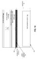
- FIG. 1 illustrates pixel 100 of a backside illuminated ("BSI") image sensor having a negative charge layer 127, in accordance with an embodiment of the disclosure.
- Pixel 100 includes microlens 113, color filter 117, anti-reflection element 120, insulation layer 130, semiconductor substrate 140, and metal layers 150.
- Anti-reflection element 120 includes a charge sinking layer 123 and a negative charge layer 127.
- Negative charge layer 127 retains negative fixed electric charge and is negatively charged.
- Charge sinking layer 123 functions to sink positive charge from negative charge layer 127. Sinking the positive charge from negative charge layer 127 increases or retains the negative charge of negative charge layer 127. In order to "sink" positive charge from negative charge layer 127, charge sinking layer 123 may be positively charged (i.e. it retains positive fixed electric charge). In some cases, the charge sinking layer may actually supply electrons to the negative charge layer.
- negative charge layer 127 is disposed proximate to semiconductor substrate 140 to induce holes in an accumulation zone in the semiconductor substrate.
- Charge sinking layer 123 holds the negative charge in the negative charge layer 127 in place, which in turn enables negative charge layer 127 to hold the holes in the accumulation zone in place at an acceptable hole density.
- the combination of charge sinking layer 123 and negative charge layer 127 is referred to as an anti-reflection element 120 because the thicknesses of the layers 123 and 127 are sized to be substantially anti-reflective so that image light 105 travels to photosensitive element 145 without being reflected at the interfaces of layers 123 and 127.
- the thicknesses of layers 123 and 127 may be sized based on an index of refraction of each layer, while also taking into consideration the wavelength of image light 105. Additional consideration will be taken in sizing the thickness of charge sinking layer 123 and negative charge layer 127 for anti-reflection in embodiments where there are more layers between color filter 117 and insulation layer 130 than are shown in FIG. 1 .
- Metal layers 150 may include metal interconnects configured to facilitate readout of pixel 100.
- metal layer 150 may include an electrode of a transfer gate (not shown) for transferring electrons (generated by photons from image light 105) in photosensitive element 145 to a floating diffusion region.
- the floating diffusion region (not shown) may also be located in semiconductor substrate 140.
- image light 105 propagates along an optical path that encounters microlens 113, color filter 117, charge sinking layer 123, negative charge layer 127, insulation layer 130, and semiconductor substrate 145, in that order. In other embodiments, some of the layers may be rearranged or have layers added or subtracted. In some embodiments, a color filter 117 may not be included.
- microlens 113 focuses or condenses the image light (for optical efficiency) to direct image light 105 to photosensitive element 145.
- image light 105 is incident on photosensitive element 145 and photosensitive element 145 generates an electrical signal (photo-generated charge) in response to the incident light.
- the electrical signal is held in photosensitive element 145.
- a transfer gate (not shown) may be off. When the integration period is over, the transfer gate may turn on and, allowing the electrons from photosensitive element 145 to transfer into the floating diffusion region, which will later be readout by readout circuitry of an image sensor.
- FIGs. 2-11 illustrate examples of layers that may be disposed between microlens 113 and metal layers 150. Those skilled in the art will understand that additional layers that are not shown in FIGs. 2-11 may also be included between microlens 113 and metal layers 150. For example, additional optic layers (e.g. infrared filter) and/or oxide and metal grid layers may be included.
- additional optic layers e.g. infrared filter
- oxide and metal grid layers may be included.
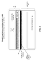
- FIG. 2 illustrates example layers of a pixel of a BSI image sensor having a negative charge layer, in accordance with an embodiment of the disclosure.
- Semiconductor substrate 140 includes a light-receiving surface 241.
- light-receiving surface 241 is on the backside of semiconductor 140, as the illustrated layers are for a BSI image sensor.
- light-receiving surface 241 receives image light 105 before the frontside surface 242 of semiconductor substrate 140, which is the surface opposite of light-receiving surface 241 in FIG. 2 .
- the negative charge layer 227 is made out of hafnium-aluminum-oxide (HfAl x O y ). In some examples, there may be small amounts of other elements in the negative charge layer, but in those examples, the negative charge layer will still be primarily hafnium-aluminum-oxide. Hafnium-aluminum-oxide is inherently a negatively charged substance. As shown in FIG. 2 , insulation layer 130 (which may be silicon-dioxide) provides a thin layer between negative charge layer 227 and semiconductor substrate 140.
- hafnium-aluminum-oxide is inherently a negatively charged substance, its proximity to substrate 140 (being disposed along light-receiving surface 241) induces holes to form in an accumulation zone 243 near the light-receiving surface 241.
- Charge sinking layer 223 may be made from Tantalum-oxide (e.g. Ta 2 O 5 ), which is an inherently positively charged substance that holds the negative charge in the negative charge layer 227 in place, which in turn can hold the holes in accumulation zone 243 in place.
- the accumulated holes in accumulation zone 243 reduce dark current that may be generated as a result of the interface between semiconductor substrate 140 and insulation layer 130 from becoming part of the image signal generated by photosensitive element 145. Consequently, the performance of the BSI image sensor is enhanced.
- hafnium-oxide HfO2
- titanium-oxide TiO2
- zirconium-oxide ZrO2
- tantalum-oxide Ta2O5
- aluminum oxide Al203
- hafnium-aluminum-oxide as a negative charge layer.
- Applicants' experimentation and data analysis indicate that the properties of hafnium-aluminum-oxide offer improved performance over conventional negative charge layers.
- hafnium-aluminum-oxide provides more stabilized (over time) negative fixed charge than conventional metal oxides used in negative charge layers.
- Applicants' data shows that hafnium-aluminum-oxide induces a higher density of holes in accumulation zone 243, which reduces dark current more proficiently than conventional negative charge layers.
- This hole inducing property of hafnium-aluminum-oxide may be derived from hafnium-aluminum-oxide's ability to retain and hold more negative charge than conventional negative charge layers, given the same thickness.
- the optical properties of the negative charge layer are also important to configuring anti-reflection element 220, being able to induce a greater hole density in accumulation zone 243 may allow the negative charge layer 227 to have a smaller thickness than conventional solutions.
- FIG. 3 shows a chart illustrating the position of layers in a pixel in relation to the energy required for electrons to transfer between the layers of FIG. 2 , in accordance with an embodiment of the disclosure.
- FIG. 3 shows that a silicon-oxide layer is disposed between a silicon layer and a hafnium-aluminum-oxide layer. And, the hafnium-aluminum-oxide is disposed between the silicon oxide layer and the Tantalum-oxide layer.
- the illustrated silicon layer is an example of a substrate layer
- the silicon-oxide layer is an example of an insulator layer
- the hafnium-aluminum-oxide layer is an example of a negative charge layer
- the Tantalum-oxide layer is an example of a charge sinking layer.
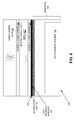
- FIG. 4 illustrates example layers of a pixel of a backside illuminated image sensor having a graded negative charge layer, in accordance with an embodiment of the disclosure.
- the embodiment illustrated in FIG. 4 differs from the embodiment illustrated in FIG. 2 because the negative charge layer 427 has a graded distribution of aluminum in the hafnium-aluminum-oxide. More specifically, there is a greater distribution of aluminum proximate to the top side (closest to charge sinking layer 223) of the negative charge layer 427 than to a bottom side (closest to insulation layer 130) of the negative charge layer 427.
- negative charge layer 227 illustrated in FIG. 2 has substantially uniform distribution of aluminum in the hafnium-aluminum-oxide.
- FIG. 5 shows a chart illustrating the position of layers in a pixel in relation to the energy required for electrons to transfer between the layers of FIG. 4 , in accordance with an embodiment of the disclosure.
- the chart of FIG. 5 differs from the chart of FIG. 3 in that the hafnium-aluminum-oxide layer is tapered as it gets closer in position to the silicon layer. This shows that as a negatively charged carrier retained by negative charge layer 427 gets closer to the charge sinking layer (e.g. Ta 2 O 5 ), it should require a higher amount of energy to transfer to the charge sinking layer.
- the charge sinking layer e.g. Ta 2 O 5
- the hafnium-aluminum-oxide layer gets richer in aluminum as it gets closer to the charge sinking layer, and the increased aluminum content provides a better barrier to negatively charged carriers that could potentially combine with positively charge carriers in the charge sinking layer (illustrated as Ta 2 O 5 ). Therefore, having a graded negatively charged layer can reduce the amount of recombination interaction between the negatively charged layer and the positively charged layer. Consequently, the negatively charged layer will be better able to retain its negative charge to induce holes in accumulation zone 243.
- an atomic layer deposition (“ALD”) process can be used to lay down sub-layers of hafnium-aluminum-oxide.
- ALD atomic layer deposition
- one or more initial sub-layers of hafnium-aluminum-oxide may be deposited on insulation layer 130 using ALD.
- the initial sub-layers will form hafnium-aluminum-oxide with a first concentration/distribution of aluminum.
- Subsequently deposited sub-layers of hafnium-aluminum-oxide will have a concentration/distribution of aluminum that is greater than the initial sub-layers, which forms the graded distribution of aluminum.
- the grading of the distribution of aluminum in the hafnium-aluminum-oxide layer may be gradual (as illustrated by the smooth taper of HfAlO in FIG. 5 ) or may be more abrupt or stair stepped.
- the concentration/distribution of aluminum in the hafnium-aluminum-oxide can be substantially the same as each sub-layer is formed using ALD.
- FIG. 6 illustrates example layers of a pixel of a backside illuminated image sensor having a negative charge layer and a charge sinking layer, in accordance with an embodiment of the disclosure.
- a first charge blocking barrier layer 633 is disposed between insulator 130 and negative charge layer 627 and a second charging blocking layer 634 is disposed between charge sinking layer 223 and negative charge layer 627.
- Charge blocking barrier layers 633 and 634 may be made from aluminum-oxide (Al 2 O 3 ).
- one or more of charge blocking barrier layer 633 and 634 is made from hafnium-aluminum-oxide having an increased aluminum concentration.
- negative charge layer 627 is illustrated as including HfO 2 , but in some embodiments, negative charge layer 627 may be made from hafnium-aluminum-oxide having a decreased aluminum concentration.
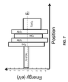
- FIG. 7 shows a chart illustrating the position of layers in a pixel in relation to the energy required for electrons to transfer between the layers of FIG. 6 , in accordance with an embodiment of the disclosure.
- FIG. 7 shows layers from left to right as a silicon layer (substrate), silicon-oxide layer (insulation layer), aluminum-oxide (charge blocking barrier), hafnium-oxide layer (example of negative charge layer), aluminum-oxide (charge blocking barrier), and tantalum-oxide layer (example of a charge sinking layer).
- FIG. 8 illustrates example layers of a pixel of a backside illuminated image sensor having a negative charge layer and a charge sinking layer, in accordance with an embodiment of the disclosure.
- a charge blocking barrier layer 634 is disposed between charge sinking layer 223 and negative charge layer 627.
- Charge blocking barrier layer 634 may be made from aluminum-oxide (Al 2 O 3 ).
- charge blocking barrier layer 634 is made from hafnium-aluminum-oxide having a high aluminum concentration.
- Charge blocking barrier 634 blocks electron migration between layers 223 and 627, which helps maintain the desired electrical charge of the layers.
- negative charge layer 627 is illustrated as including HfO 2 , but in some embodiments, negative charge layer 627 may be made from hafnium-aluminum-oxide having a low aluminum concentration.
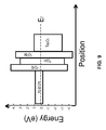
- FIG. 9 shows a chart illustrating the position of layers in a pixel in relation to the energy required for electrons to transfer between the layers of FIG. 8 , in accordance with an embodiment of the disclosure.
- FIG. 9 shows layers from left to right as a silicon layer (substrate), silicon-oxide layer (insulation layer), hafnium-oxide layer (example of negative charge layer), aluminum-oxide (charge blocking barrier), and tantalum-oxide layer (example of a charge sinking layer).
- FIG. 10 illustrates example layers of a pixel of a backside illuminated image sensor having a negative charge layer and a charge sinking layer, in accordance with an embodiment of the disclosure.
- a charge blocking barrier layer 634 is disposed between charge sinking layer 223 and negative charge layer 627.
- Charge blocking barrier layer 634 may be made from aluminum-oxide (Al 2 O 3 ).
- charge blocking barrier layer 634 is made from hafnium-aluminum-oxide having a high aluminum concentration. Charge blocking barrier 634 blocks electron migration between layers 223 and 627, which helps maintain the desired electrical charge of the layers.
- negative charge layer 627 is illustrated as including HfO 2 , but in some embodiments, negative charge layer 627 may be made from hafnium-aluminum-oxide having a low aluminum concentration. Also included in FIG. 10 is an oxygen barrier layer 635. Oxygen barrier layer 635 may be made from aluminum-oxide (AL 2 O 3 ), which has a low diffusion coefficient of oxygen that decreases oxygen diffusing into charge sinking layer 223. Oxygen diffusion into charge sinking layer 223 can detrimentally influence the desired electrical charge of the charge sinking layer, which is why it may be desirable to prevent oxygen diffusion into it.
- AL 2 O 3 aluminum-oxide
- FIG. 11 shows a chart illustrating the position of layers in a pixel in relation to the energy required for electrons to transfer between the layers of FIG. 10 , in accordance with an embodiment of the disclosure.
- FIG. 11 shows layers from left to right as a silicon layer (substrate), silicon-oxide layer (insulation layer), aluminum-oxide (charge blocking barrier), hafnium-oxide layer (example of negative charge layer), tantalum-oxide layer (example of a charge sinking layer), and aluminum-oxide (example of oxygen barrier layer).
- the charge sinking layer may actually supply electrons to the negative charge layer. This may happen if the charge sinking layer includes SI 3 N 4 (instead of Ta 2 O 5 ) and the negative charge layer includes HfO 2 .
- FIG. 12 is a block diagram illustrating an imaging system 1200, in accordance with an embodiment of the disclosure.
- the illustrated embodiment of imaging system 1200 includes a pixel array 1205, readout circuitry 1210, function logic 1215, and control circuitry 1220.
- Pixel array 1205 is a two-dimensional (“2D") array of imaging sensors or pixels (e.g., pixels P1, P2 ..., Pn).
- each pixel is a complementary metal-oxide-semiconductor ("CMOS") imaging pixel.
- CMOS complementary metal-oxide-semiconductor
- each pixel is arranged into a row (e.g., rows R1 to Ry) and a column (e.g., column C1 to Cx) to acquire image data of a person, place, or object, which can then be used to render a 2D image of the person, place, or object.
- Pixel 100 and the embodiments associated with FIGs. 1-5 may be incorporated into the pixels of pixel array 1205.
- Readout circuitry 1210 may include amplification circuitry, analog-to-digital ("ADC") conversion circuitry, or otherwise.
- Function logic 1215 may simply store the image data or even manipulate the image data by applying post image effects (e.g., crop, rotate, remove red eye, adjust brightness, adjust contrast, or otherwise).
- readout circuitry 1210 may readout a row of image data at a time along readout column lines (illustrated) or may readout the image data using a variety of other techniques (not illustrated), such as a serial readout or a full parallel readout of all pixels simultaneously.
- Control circuitry 1220 is coupled to pixel array 1205 to control operational characteristic of pixel array 1205. For example, control circuitry 1220 may generate a shutter signal for controlling image acquisition.
- FIG. 13 is a circuit diagram illustrating pixel circuitry 1300 of two four-transistor ("4T") pixels within an imaging array, in accordance with an embodiment of the disclosure.
- Pixel circuitry 1300 is one possible pixel circuitry architecture for implementing each pixel within pixel array 1205 of FIG. 12 .
- embodiments of the present disclosure are not limited to 4T pixel architectures; rather, one of ordinary skill in the art having the benefit of the instant disclosure will understand that the present teachings are also applicable to 3T designs, 5T designs, and various other pixel architectures.
- each pixel circuitry 1300 includes a photodiode PD, a transfer transistor T1, a reset transistor T2, a source-follower ("SF") transistor T3, a select transistor T4, and a storage capacitor C1.
- transfer transistor T1 receives a transfer signal TX, which transfers the charge accumulated in photodiode PD to a floating diffusion node FD.
- floating diffusion node FD may be coupled to a storage capacitor for temporarily storing image charges.
- Reset transistor T2 is coupled between a power rail VDD and the floating diffusion node FD to reset the pixel (e.g., discharge or charge the FD and the PD to a preset voltage) under control of a reset signal RST.
- the floating diffusion node FD is coupled to control the gate of SF transistor T3.
- SF transistor T3 is coupled between the power rail VDD and select transistor T4.
- SF transistor T3 operates as a source-follower providing a high impedance connection to the floating diffusion FD.
- select transistor T4 selectively couples the output of pixel circuitry 1300 to the readout column line under control of a select signal SEL.
- the TX signal, the RST signal, and the SEL signal are generated by control circuitry 1220.
Landscapes
- Solid State Image Pick-Up Elements (AREA)
- Transforming Light Signals Into Electric Signals (AREA)
Abstract
Description
- This disclosure relates generally to image sensors, and in particular but not exclusively, relates to backside illuminated image sensors.
- Image sensors are widely used in digital still cameras, cellular phones, security cameras, as well as in, medical, automobile, and other applications. Complementary metal-oxide-semiconductor ("CMOS") technology is used to manufacture lower cost image sensors on silicon substrates. In a large number of image sensors, the image sensor commonly includes hundreds, thousand or even millions of light sensor cells or pixels.
- Backside illuminated ("BSI") technology is often used in image sensors to increase the amount of image light that becomes incident on photosensitive elements in pixels of the image sensor. When BSI technology is used, backside accumulation helps create an electric field that directs photo-electrons (generated by incident image light) to a frontside of the image sensor where they can be collected and measured. Without accumulation on the backside the semiconductor substrate, diffusion of the electrons to the back surface may result in loss by recombination, which may degrade the sensitivity of the image sensor. Advantageously, accumulation on the backside of the semiconductor substrate can reduce or impede "dark current" generated from the semiconductor substrate's interface with another layer (e.g. silicon dioxide insulation layer). Reducing "dark current" will improve the signal-to-noise ratio of the image sensor, which importantly, improves the sensitivity of the image sensor. Given that accumulation on the backside of the semiconductor substrate is beneficial, the image sensor industry seeks to generate backside accumulation that will give image sensors improved performance.
- Non-limiting and non-exhaustive embodiments of the invention are described with reference to the following figures, wherein like reference numerals refer to like parts throughout the various views unless otherwise specified.
-
FIG. 1 illustrates one example of a pixel of a backside illuminated image sensor having a negative charge layer and a charge sinking layer, in accordance with an embodiment of the disclosure. -
FIG. 2 illustrates example layers of a pixel of a backside illuminated image sensor having a negative charge layer and a charge sinking layer, in accordance with an embodiment of the disclosure. -
FIG. 3 shows a chart illustrating the position of layers in a pixel in relation to the energy required for electrons to transfer between the layers ofFIG. 2 , in accordance with an embodiment of the disclosure. -
FIG. 4 illustrates example layers of a pixel of a backside illuminated image sensor having a graded negative charge layer and a charge sinking layer, in accordance with an embodiment of the disclosure. -
FIG. 5 shows a chart illustrating the position of layers in a pixel in relation to the energy required for electrons to transfer between the layers ofFIG. 4 , in accordance with an embodiment of the disclosure. -
FIG. 6 illustrates example layers of a pixel of a backside illuminated image sensor having a negative charge layer and a charge sinking layer, in accordance with an embodiment of the disclosure. -
FIG. 7 shows a chart illustrating the position of layers in a pixel in relation to the energy required for electrons to transfer between the layers ofFIG. 6 , in accordance with an embodiment of the disclosure. -
FIG. 8 illustrates example layers of a pixel of a backside illuminated image sensor having a negative charge layer and a charge sinking layer, in accordance with an embodiment of the disclosure. -
FIG. 9 shows a chart illustrating the position of layers in a pixel in relation to the energy required for electrons to transfer between the layers ofFIG. 8 , in accordance with an embodiment of the disclosure. -
FIG. 10 illustrates example layers of a pixel of a backside illuminated image sensor having a negative charge layer and a charge sinking layer, in accordance with an embodiment of the disclosure. -
FIG. 11 shows a chart illustrating the position of layers in a pixel in relation to the energy required for electrons to transfer between the layers ofFIG. 10 , in accordance with an embodiment of the disclosure. -
FIG. 12 is a block diagram illustrating an imaging system, in accordance with an embodiment of the disclosure. -
FIG. 13 is a circuit diagram illustrating pixel circuitry of two four-transistor ("4T") pixels within an imaging array, in accordance with an embodiment of the disclosure. - Embodiments of an image sensor and an imaging system are described herein. In the following description, numerous specific details are set forth to provide a thorough understanding of the embodiments. One skilled in the relevant art will recognize, however, that the techniques described herein can be practiced without one or more of the specific details, or with other methods, components, materials, etc. In other instances, well-known structures, materials, or operations are not shown or described in detail to avoid obscuring certain aspects.
- Reference throughout this specification to "one embodiment" or "an embodiment" means that a particular feature, structure, or characteristic described in connection with the embodiment is included in at least one embodiment of the present invention. Thus, the appearances of the phrases "in one embodiment" or "in an embodiment" in various places throughout this specification are not necessarily all referring to the same embodiment. Furthermore, the particular features, structures, or characteristics may be combined in any suitable manner in one or more embodiments.
-
FIG. 1 illustratespixel 100 of a backside illuminated ("BSI") image sensor having anegative charge layer 127, in accordance with an embodiment of the disclosure.Pixel 100 includesmicrolens 113,color filter 117,anti-reflection element 120,insulation layer 130,semiconductor substrate 140, andmetal layers 150.Anti-reflection element 120 includes acharge sinking layer 123 and anegative charge layer 127. -
Negative charge layer 127 retains negative fixed electric charge and is negatively charged.Charge sinking layer 123 functions to sink positive charge fromnegative charge layer 127. Sinking the positive charge fromnegative charge layer 127 increases or retains the negative charge ofnegative charge layer 127. In order to "sink" positive charge fromnegative charge layer 127, chargesinking layer 123 may be positively charged (i.e. it retains positive fixed electric charge). In some cases, the charge sinking layer may actually supply electrons to the negative charge layer. - As will be explained in more detail,
negative charge layer 127 is disposed proximate tosemiconductor substrate 140 to induce holes in an accumulation zone in the semiconductor substrate.Charge sinking layer 123 holds the negative charge in thenegative charge layer 127 in place, which in turn enablesnegative charge layer 127 to hold the holes in the accumulation zone in place at an acceptable hole density. - The combination of
charge sinking layer 123 andnegative charge layer 127 is referred to as ananti-reflection element 120 because the thicknesses of thelayers image light 105 travels tophotosensitive element 145 without being reflected at the interfaces oflayers layers image light 105. Additional consideration will be taken in sizing the thickness of charge sinkinglayer 123 andnegative charge layer 127 for anti-reflection in embodiments where there are more layers betweencolor filter 117 andinsulation layer 130 than are shown inFIG. 1 . -
Semiconductor substrate 140 includes aphotosensitive element 145 for accumulating charge in response toincident image light 105.Metal layers 150 may include metal interconnects configured to facilitate readout ofpixel 100. For example,metal layer 150 may include an electrode of a transfer gate (not shown) for transferring electrons (generated by photons from image light 105) inphotosensitive element 145 to a floating diffusion region. The floating diffusion region (not shown) may also be located insemiconductor substrate 140. - In the illustrated embodiment,
image light 105 propagates along an optical path that encountersmicrolens 113,color filter 117,charge sinking layer 123,negative charge layer 127,insulation layer 130, andsemiconductor substrate 145, in that order. In other embodiments, some of the layers may be rearranged or have layers added or subtracted. In some embodiments, acolor filter 117 may not be included. Whenimage light 105 encountersmicrolens 113 along the optical path,microlens 113 focuses or condenses the image light (for optical efficiency) to directimage light 105 tophotosensitive element 145. During an integration period (also referred to as an exposure or accumulation period),image light 105 is incident onphotosensitive element 145 andphotosensitive element 145 generates an electrical signal (photo-generated charge) in response to the incident light. The electrical signal is held inphotosensitive element 145. At this stage, a transfer gate (not shown) may be off. When the integration period is over, the transfer gate may turn on and, allowing the electrons fromphotosensitive element 145 to transfer into the floating diffusion region, which will later be readout by readout circuitry of an image sensor. -
FIGs. 2-11 illustrate examples of layers that may be disposed betweenmicrolens 113 andmetal layers 150. Those skilled in the art will understand that additional layers that are not shown inFIGs. 2-11 may also be included betweenmicrolens 113 andmetal layers 150. For example, additional optic layers (e.g. infrared filter) and/or oxide and metal grid layers may be included. -
FIG. 2 illustrates example layers of a pixel of a BSI image sensor having a negative charge layer, in accordance with an embodiment of the disclosure.Semiconductor substrate 140 includes a light-receivingsurface 241. In the illustrated embodiment, light-receivingsurface 241 is on the backside ofsemiconductor 140, as the illustrated layers are for a BSI image sensor. In other words, light-receivingsurface 241 receives image light 105 before thefrontside surface 242 ofsemiconductor substrate 140, which is the surface opposite of light-receivingsurface 241 inFIG. 2 . - In
FIG. 2 , the negative charge layer 227 is made out of hafnium-aluminum-oxide (HfAlxOy). In some examples, there may be small amounts of other elements in the negative charge layer, but in those examples, the negative charge layer will still be primarily hafnium-aluminum-oxide. Hafnium-aluminum-oxide is inherently a negatively charged substance. As shown inFIG. 2 , insulation layer 130 (which may be silicon-dioxide) provides a thin layer between negative charge layer 227 andsemiconductor substrate 140. However, since hafnium-aluminum-oxide is inherently a negatively charged substance, its proximity to substrate 140 (being disposed along light-receiving surface 241) induces holes to form in anaccumulation zone 243 near the light-receivingsurface 241.Charge sinking layer 223 may be made from Tantalum-oxide (e.g. Ta2O5), which is an inherently positively charged substance that holds the negative charge in the negative charge layer 227 in place, which in turn can hold the holes inaccumulation zone 243 in place. The accumulated holes inaccumulation zone 243 reduce dark current that may be generated as a result of the interface betweensemiconductor substrate 140 andinsulation layer 130 from becoming part of the image signal generated byphotosensitive element 145. Consequently, the performance of the BSI image sensor is enhanced. - In conventional BSI image sensors, various two element metal oxides have been used as a negative charge layer proximate to the semiconductor substrate. For example, hafnium-oxide (HfO2), titanium-oxide (TiO2), zirconium-oxide (ZrO2), tantalum-oxide (Ta2O5), and aluminum oxide (Al203) have been used as negative charge layers. However, Applicants propose using a hafnium-aluminum-oxide as a negative charge layer. Applicants' experimentation and data analysis indicate that the properties of hafnium-aluminum-oxide offer improved performance over conventional negative charge layers. Unexpectedly, experiments indicate that hafnium-aluminum-oxide provides more stabilized (over time) negative fixed charge than conventional metal oxides used in negative charge layers. In addition, Applicants' data shows that hafnium-aluminum-oxide induces a higher density of holes in
accumulation zone 243, which reduces dark current more proficiently than conventional negative charge layers. This hole inducing property of hafnium-aluminum-oxide may be derived from hafnium-aluminum-oxide's ability to retain and hold more negative charge than conventional negative charge layers, given the same thickness. Furthermore, since the optical properties of the negative charge layer are also important to configuringanti-reflection element 220, being able to induce a greater hole density inaccumulation zone 243 may allow the negative charge layer 227 to have a smaller thickness than conventional solutions. -
FIG. 3 shows a chart illustrating the position of layers in a pixel in relation to the energy required for electrons to transfer between the layers ofFIG. 2 , in accordance with an embodiment of the disclosure.FIG. 3 shows that a silicon-oxide layer is disposed between a silicon layer and a hafnium-aluminum-oxide layer. And, the hafnium-aluminum-oxide is disposed between the silicon oxide layer and the Tantalum-oxide layer. The illustrated silicon layer is an example of a substrate layer, the silicon-oxide layer is an example of an insulator layer, the hafnium-aluminum-oxide layer is an example of a negative charge layer, and the Tantalum-oxide layer is an example of a charge sinking layer. -
FIG. 4 illustrates example layers of a pixel of a backside illuminated image sensor having a graded negative charge layer, in accordance with an embodiment of the disclosure. The embodiment illustrated inFIG. 4 differs from the embodiment illustrated inFIG. 2 because thenegative charge layer 427 has a graded distribution of aluminum in the hafnium-aluminum-oxide. More specifically, there is a greater distribution of aluminum proximate to the top side (closest to charge sinking layer 223) of thenegative charge layer 427 than to a bottom side (closest to insulation layer 130) of thenegative charge layer 427. In contrast, negative charge layer 227 illustrated inFIG. 2 has substantially uniform distribution of aluminum in the hafnium-aluminum-oxide. -
FIG. 5 shows a chart illustrating the position of layers in a pixel in relation to the energy required for electrons to transfer between the layers ofFIG. 4 , in accordance with an embodiment of the disclosure. The chart ofFIG. 5 differs from the chart ofFIG. 3 in that the hafnium-aluminum-oxide layer is tapered as it gets closer in position to the silicon layer. This shows that as a negatively charged carrier retained bynegative charge layer 427 gets closer to the charge sinking layer (e.g. Ta2O5), it should require a higher amount of energy to transfer to the charge sinking layer. This is because the hafnium-aluminum-oxide layer gets richer in aluminum as it gets closer to the charge sinking layer, and the increased aluminum content provides a better barrier to negatively charged carriers that could potentially combine with positively charge carriers in the charge sinking layer (illustrated as Ta2O5). Therefore, having a graded negatively charged layer can reduce the amount of recombination interaction between the negatively charged layer and the positively charged layer. Consequently, the negatively charged layer will be better able to retain its negative charge to induce holes inaccumulation zone 243. - To manufacture the graded negative charge layer illustrated in
FIGs. 4 and5 , an atomic layer deposition ("ALD") process can be used to lay down sub-layers of hafnium-aluminum-oxide. After theinsulation layer 130 is formed, one or more initial sub-layers of hafnium-aluminum-oxide may be deposited oninsulation layer 130 using ALD. The initial sub-layers will form hafnium-aluminum-oxide with a first concentration/distribution of aluminum. Subsequently deposited sub-layers of hafnium-aluminum-oxide will have a concentration/distribution of aluminum that is greater than the initial sub-layers, which forms the graded distribution of aluminum. The grading of the distribution of aluminum in the hafnium-aluminum-oxide layer may be gradual (as illustrated by the smooth taper of HfAlO inFIG. 5 ) or may be more abrupt or stair stepped. Of course, to manufacture the negative charge layer illustrated inFIGs. 2 and3 , the concentration/distribution of aluminum in the hafnium-aluminum-oxide can be substantially the same as each sub-layer is formed using ALD. -
FIG. 6 illustrates example layers of a pixel of a backside illuminated image sensor having a negative charge layer and a charge sinking layer, in accordance with an embodiment of the disclosure. InFIG. 6 , a first charge blockingbarrier layer 633 is disposed betweeninsulator 130 andnegative charge layer 627 and a secondcharging blocking layer 634 is disposed betweencharge sinking layer 223 andnegative charge layer 627. Charge blockingbarrier layers barrier layer Charge blocking barriers layers substrate 140, which helps maintain the desired electrical charge of the layers. InFIG. 6 ,negative charge layer 627 is illustrated as including HfO2, but in some embodiments,negative charge layer 627 may be made from hafnium-aluminum-oxide having a decreased aluminum concentration. -
FIG. 7 shows a chart illustrating the position of layers in a pixel in relation to the energy required for electrons to transfer between the layers ofFIG. 6 , in accordance with an embodiment of the disclosure.FIG. 7 shows layers from left to right as a silicon layer (substrate), silicon-oxide layer (insulation layer), aluminum-oxide (charge blocking barrier), hafnium-oxide layer (example of negative charge layer), aluminum-oxide (charge blocking barrier), and tantalum-oxide layer (example of a charge sinking layer). -
FIG. 8 illustrates example layers of a pixel of a backside illuminated image sensor having a negative charge layer and a charge sinking layer, in accordance with an embodiment of the disclosure. InFIG. 8 , a chargeblocking barrier layer 634 is disposed betweencharge sinking layer 223 andnegative charge layer 627. Charge blockingbarrier layer 634 may be made from aluminum-oxide (Al2O3). In one embodiment, charge blockingbarrier layer 634 is made from hafnium-aluminum-oxide having a high aluminum concentration. Charge blockingbarrier 634 blocks electron migration betweenlayers FIG. 8 ,negative charge layer 627 is illustrated as including HfO2, but in some embodiments,negative charge layer 627 may be made from hafnium-aluminum-oxide having a low aluminum concentration. -
FIG. 9 shows a chart illustrating the position of layers in a pixel in relation to the energy required for electrons to transfer between the layers ofFIG. 8 , in accordance with an embodiment of the disclosure.FIG. 9 shows layers from left to right as a silicon layer (substrate), silicon-oxide layer (insulation layer), hafnium-oxide layer (example of negative charge layer), aluminum-oxide (charge blocking barrier), and tantalum-oxide layer (example of a charge sinking layer). -
FIG. 10 illustrates example layers of a pixel of a backside illuminated image sensor having a negative charge layer and a charge sinking layer, in accordance with an embodiment of the disclosure. InFIG. 10 , a chargeblocking barrier layer 634 is disposed betweencharge sinking layer 223 andnegative charge layer 627. Charge blockingbarrier layer 634 may be made from aluminum-oxide (Al2O3). In one embodiment, charge blockingbarrier layer 634 is made from hafnium-aluminum-oxide having a high aluminum concentration. Charge blockingbarrier 634 blocks electron migration betweenlayers FIG. 10 ,negative charge layer 627 is illustrated as including HfO2, but in some embodiments,negative charge layer 627 may be made from hafnium-aluminum-oxide having a low aluminum concentration. Also included inFIG. 10 is anoxygen barrier layer 635.Oxygen barrier layer 635 may be made from aluminum-oxide (AL2O3), which has a low diffusion coefficient of oxygen that decreases oxygen diffusing intocharge sinking layer 223. Oxygen diffusion intocharge sinking layer 223 can detrimentally influence the desired electrical charge of the charge sinking layer, which is why it may be desirable to prevent oxygen diffusion into it. -
FIG. 11 shows a chart illustrating the position of layers in a pixel in relation to the energy required for electrons to transfer between the layers ofFIG. 10 , in accordance with an embodiment of the disclosure.FIG. 11 shows layers from left to right as a silicon layer (substrate), silicon-oxide layer (insulation layer), aluminum-oxide (charge blocking barrier), hafnium-oxide layer (example of negative charge layer), tantalum-oxide layer (example of a charge sinking layer), and aluminum-oxide (example of oxygen barrier layer). - With regard to the embodiments associated with
FIGs. 6-11 , in some cases, the charge sinking layer may actually supply electrons to the negative charge layer. This may happen if the charge sinking layer includes SI3N4 (instead of Ta2O5) and the negative charge layer includes HfO2. -
FIG. 12 is a block diagram illustrating animaging system 1200, in accordance with an embodiment of the disclosure. The illustrated embodiment ofimaging system 1200 includes apixel array 1205,readout circuitry 1210,function logic 1215, andcontrol circuitry 1220. -
Pixel array 1205 is a two-dimensional ("2D") array of imaging sensors or pixels (e.g., pixels P1, P2 ..., Pn). In one embodiment, each pixel is a complementary metal-oxide-semiconductor ("CMOS") imaging pixel. As illustrated, each pixel is arranged into a row (e.g., rows R1 to Ry) and a column (e.g., column C1 to Cx) to acquire image data of a person, place, or object, which can then be used to render a 2D image of the person, place, or object.Pixel 100 and the embodiments associated withFIGs. 1-5 may be incorporated into the pixels ofpixel array 1205. - After each pixel has acquired its image data or image charge, the image data is readout by
readout circuitry 1210 and transferred to functionlogic 1215.Readout circuitry 1210 may include amplification circuitry, analog-to-digital ("ADC") conversion circuitry, or otherwise.Function logic 1215 may simply store the image data or even manipulate the image data by applying post image effects (e.g., crop, rotate, remove red eye, adjust brightness, adjust contrast, or otherwise). In one embodiment,readout circuitry 1210 may readout a row of image data at a time along readout column lines (illustrated) or may readout the image data using a variety of other techniques (not illustrated), such as a serial readout or a full parallel readout of all pixels simultaneously.Control circuitry 1220 is coupled topixel array 1205 to control operational characteristic ofpixel array 1205. For example,control circuitry 1220 may generate a shutter signal for controlling image acquisition. -
FIG. 13 is a circuit diagram illustratingpixel circuitry 1300 of two four-transistor ("4T") pixels within an imaging array, in accordance with an embodiment of the disclosure.Pixel circuitry 1300 is one possible pixel circuitry architecture for implementing each pixel withinpixel array 1205 ofFIG. 12 . However, it should be appreciated that embodiments of the present disclosure are not limited to 4T pixel architectures; rather, one of ordinary skill in the art having the benefit of the instant disclosure will understand that the present teachings are also applicable to 3T designs, 5T designs, and various other pixel architectures. - In
FIG. 13 , pixels Pa and Pb are arranged in two rows and one column. The illustrated embodiment of eachpixel circuitry 1300 includes a photodiode PD, a transfer transistor T1, a reset transistor T2, a source-follower ("SF") transistor T3, a select transistor T4, and a storage capacitor C1. During operation, transfer transistor T1 receives a transfer signal TX, which transfers the charge accumulated in photodiode PD to a floating diffusion node FD. In one embodiment, floating diffusion node FD may be coupled to a storage capacitor for temporarily storing image charges. - Reset transistor T2 is coupled between a power rail VDD and the floating diffusion node FD to reset the pixel (e.g., discharge or charge the FD and the PD to a preset voltage) under control of a reset signal RST. The floating diffusion node FD is coupled to control the gate of SF transistor T3. SF transistor T3 is coupled between the power rail VDD and select transistor T4. SF transistor T3 operates as a source-follower providing a high impedance connection to the floating diffusion FD. Finally, select transistor T4 selectively couples the output of
pixel circuitry 1300 to the readout column line under control of a select signal SEL. In one embodiment, the TX signal, the RST signal, and the SEL signal are generated bycontrol circuitry 1220. - The above description of illustrated embodiments of the invention, including what is described in the Abstract, is not intended to be exhaustive or to limit the invention to the precise forms disclosed. While specific embodiments of, and examples for, the invention are described herein for illustrative purposes, various modifications are possible within the scope of the invention, as those skilled in the relevant art will recognize.
- These modifications can be made to the invention in light of the above detailed description. The terms used in the following claims should not be construed to limit the invention to the specific embodiments disclosed in the specification. Rather, the scope of the invention is to be determined entirely by the following claims, which are to be construed in accordance with established doctrines of claim interpretation.
Claims (13)
- An image sensor comprising:a semiconductor substrate including a photosensitive element for accumulating charge in response to incident image light, wherein the semiconductor substrate includes a light-receiving surface positioned to receive the image light;a negative charge layer disposed proximate to the light-receiving surface of the semiconductor substrate to induce holes in an accumulation zone in the semiconductor substrate along the light-receiving surface; anda charge sinking layer disposed proximate to the negative charge layer, wherein the charge sinking layer is configured to conserve or increase an amount of negative charge in the negative charge layer, and wherein the negative charge layer is disposed between the semiconductor substrate and the charge sinking layer.
- The image sensor of claim 1, wherein the negative charge layer includes hafnium-aluminum-oxide.
- The image sensor of claim 2, wherein the negative charge layer includes a graded distribution of aluminum in the hafnium-aluminum-oxide, the hafnium-aluminum-oxide including a greater distribution of aluminum proximate to a top side of the negative charge layer than proximate to a bottom side of the negative charge layer, the bottom side in closer proximity to the photosensitive element than the top side.
- The image sensor of claim 3, wherein the graded distribution is a gradual increase in the aluminum content.
- The image sensor of claim 3, wherein the graded distribution is a step-wise increase in the aluminum content.
- The image sensor of claim 2, wherein the aluminum in the hafnium-aluminum-oxide is distributed substantially uniformly.
- The image sensor of claim 1, wherein the charge sinking layer is positively charged.
- The image sensor of claim 1, wherein the image sensor is a backside illuminated image sensor ("BSI") and the light-receiving surface is a backside of the BSI.
- The image sensor of claim 1, wherein a first thickness of the negative charge layer and a second thickness of the charge sinking layer are configured to reduce an amount of reflection of the image light.
- The image sensor of claim 1 further comprising:an insulation layer disposed between the negative charge layer and the semiconductor substrate; anda first charge blocking barrier layer ("CBBL") disposed between the negative charge layer and the charge sinking layer.
- The image sensor of claim 10 further comprising:a second CBBL disposed between the insulation layer and the negative charge layer.
- The image sensor of claim 1 further comprising:a first charge blocking barrier layer ("CBBL") disposed between the negative charge layer and the charge sinking layer; andan oxygen barrier disposed on a side of the charge sinking layer that is opposite the first CBBL.
- An imaging device comprising:an array of imaging pixels; andreadout circuitry coupled to the array of imaging pixels to readout image data from each of the imaging pixels in the array, wherein each imaging pixel includes:an image sensor in accordance with any of claims 1-12.
Applications Claiming Priority (1)
| Application Number | Priority Date | Filing Date | Title |
|---|---|---|---|
| US13/856,993 US9224881B2 (en) | 2013-04-04 | 2013-04-04 | Layers for increasing performance in image sensors |
Publications (2)
| Publication Number | Publication Date |
|---|---|
| EP2787532A1 true EP2787532A1 (en) | 2014-10-08 |
| EP2787532B1 EP2787532B1 (en) | 2017-10-11 |
Family
ID=50442370
Family Applications (1)
| Application Number | Title | Priority Date | Filing Date |
|---|---|---|---|
| EP14163445.1A Active EP2787532B1 (en) | 2013-04-04 | 2014-04-03 | Layers for increasing performance in image sensors |
Country Status (6)
| Country | Link |
|---|---|
| US (1) | US9224881B2 (en) |
| EP (1) | EP2787532B1 (en) |
| JP (1) | JP5990812B2 (en) |
| KR (1) | KR101560086B1 (en) |
| CN (1) | CN104103654B (en) |
| TW (1) | TWI520321B (en) |
Families Citing this family (13)
| Publication number | Priority date | Publication date | Assignee | Title |
|---|---|---|---|---|
| JP5151375B2 (en) * | 2007-10-03 | 2013-02-27 | ソニー株式会社 | Solid-state imaging device, manufacturing method thereof, and imaging device |
| JP2015032717A (en) * | 2013-08-02 | 2015-02-16 | 株式会社東芝 | Solid-state imaging device and camera module |
| US20150279880A1 (en) * | 2014-03-31 | 2015-10-01 | Taiwan Semiconductor Manufacturing Company Ltd. | Backside illuminated image sensor and method of manufacturing the same |
| US9461088B2 (en) * | 2014-12-01 | 2016-10-04 | Omnivision Technologies, Inc. | Image sensor pixel with multiple storage nodes |
| US9490282B2 (en) | 2015-03-19 | 2016-11-08 | Omnivision Technologies, Inc. | Photosensitive capacitor pixel for image sensor |
| US9876045B2 (en) * | 2015-05-06 | 2018-01-23 | Cista System Corp. | Back side illuminated CMOS image sensor arrays |
| JP6879919B2 (en) * | 2015-09-17 | 2021-06-02 | ソニーセミコンダクタソリューションズ株式会社 | Manufacturing method of solid-state image sensor, electronic device, and solid-state image sensor |
| US10163949B2 (en) | 2016-03-17 | 2018-12-25 | Taiwan Semiconductor Manufacturing Company Ltd. | Image device having multi-layered refractive layer on back surface |
| KR102666073B1 (en) * | 2016-12-28 | 2024-05-17 | 삼성전자주식회사 | Image sensor |
| CN106935605A (en) * | 2017-03-10 | 2017-07-07 | 豪威科技(上海)有限公司 | Cmos image sensor and forming method thereof |
| US10423122B2 (en) * | 2017-08-04 | 2019-09-24 | Visera Technologies Company Limited | Lens-free image sensor using phase-shifting hologram |
| CN112436026A (en) * | 2020-12-06 | 2021-03-02 | 联合微电子中心有限责任公司 | Method for reducing dark current of back-illuminated image sensor and sensor thereof |
| CN116153953B (en) * | 2022-12-23 | 2026-03-24 | 西北核技术研究所 | Dual-port CMOS image sensor pixel structure and 5T pixel structure |
Citations (5)
| Publication number | Priority date | Publication date | Assignee | Title |
|---|---|---|---|---|
| US20090209056A1 (en) * | 2008-02-19 | 2009-08-20 | Sony Corporation | Method for manufacturing solid-state imaging device |
| US20090230496A1 (en) * | 2008-03-12 | 2009-09-17 | Sony Corporation | Solid-state imaging device |
| US20110025872A1 (en) * | 2009-08-03 | 2011-02-03 | Sony Corporation | Solid-state image pickup element and a method of manufacturing the same, and image pickup device including the same |
| US20110031376A1 (en) * | 2009-03-12 | 2011-02-10 | Sony Corporation | Solid-state image pickup element, method of manufacturing the same, and image pickup apparatus including the same |
| WO2012061152A2 (en) * | 2010-10-25 | 2012-05-10 | California Institute Of Technology | Atomically precise surface engineering for producing imagers |
Family Cites Families (12)
| Publication number | Priority date | Publication date | Assignee | Title |
|---|---|---|---|---|
| JP2008192951A (en) * | 2007-02-07 | 2008-08-21 | Matsushita Electric Ind Co Ltd | Solid-state imaging device and manufacturing method thereof |
| TWI436474B (en) | 2007-05-07 | 2014-05-01 | 新力股份有限公司 | A solid-state image pickup apparatus, a manufacturing method thereof, and an image pickup apparatus |
| JP5151375B2 (en) * | 2007-10-03 | 2013-02-27 | ソニー株式会社 | Solid-state imaging device, manufacturing method thereof, and imaging device |
| KR101541544B1 (en) * | 2007-12-26 | 2015-08-03 | 소니 주식회사 | Solid-state imaging device, manufacturing method thereof, and imaging device |
| JP2010073840A (en) * | 2008-09-18 | 2010-04-02 | Sony Corp | Solid-state image sensor and method of manufacturing the same |
| JP4862878B2 (en) | 2008-10-30 | 2012-01-25 | ソニー株式会社 | Solid-state imaging device, manufacturing method thereof, and imaging device |
| GB2475086B (en) * | 2009-11-05 | 2014-02-05 | Cmosis Nv | Backside illuminated image sensor |
| JP5050063B2 (en) * | 2010-01-20 | 2012-10-17 | 株式会社東芝 | Solid-state imaging device |
| JP6226518B2 (en) * | 2011-10-24 | 2017-11-08 | 株式会社半導体エネルギー研究所 | Semiconductor device |
| US8941204B2 (en) * | 2012-04-27 | 2015-01-27 | Taiwan Semiconductor Manufacturing Company, Ltd. | Apparatus and method for reducing cross talk in image sensors |
| KR20130134292A (en) * | 2012-05-30 | 2013-12-10 | 삼성전자주식회사 | Image sensor, image processing system and method for manufacturing the image sensor |
| US8816462B2 (en) * | 2012-10-25 | 2014-08-26 | Omnivision Technologies, Inc. | Negatively charged layer to reduce image memory effect |
-
2013
- 2013-04-04 US US13/856,993 patent/US9224881B2/en active Active
- 2013-11-01 TW TW102139871A patent/TWI520321B/en active
- 2013-12-04 CN CN201310647832.8A patent/CN104103654B/en active Active
-
2014
- 2014-04-03 JP JP2014076629A patent/JP5990812B2/en active Active
- 2014-04-03 EP EP14163445.1A patent/EP2787532B1/en active Active
- 2014-04-04 KR KR1020140040569A patent/KR101560086B1/en active Active
Patent Citations (5)
| Publication number | Priority date | Publication date | Assignee | Title |
|---|---|---|---|---|
| US20090209056A1 (en) * | 2008-02-19 | 2009-08-20 | Sony Corporation | Method for manufacturing solid-state imaging device |
| US20090230496A1 (en) * | 2008-03-12 | 2009-09-17 | Sony Corporation | Solid-state imaging device |
| US20110031376A1 (en) * | 2009-03-12 | 2011-02-10 | Sony Corporation | Solid-state image pickup element, method of manufacturing the same, and image pickup apparatus including the same |
| US20110025872A1 (en) * | 2009-08-03 | 2011-02-03 | Sony Corporation | Solid-state image pickup element and a method of manufacturing the same, and image pickup device including the same |
| WO2012061152A2 (en) * | 2010-10-25 | 2012-05-10 | California Institute Of Technology | Atomically precise surface engineering for producing imagers |
Also Published As
| Publication number | Publication date |
|---|---|
| KR20140120862A (en) | 2014-10-14 |
| HK1202985A1 (en) | 2015-10-09 |
| CN104103654A (en) | 2014-10-15 |
| TW201440208A (en) | 2014-10-16 |
| KR101560086B1 (en) | 2015-10-13 |
| US20140299956A1 (en) | 2014-10-09 |
| EP2787532B1 (en) | 2017-10-11 |
| TWI520321B (en) | 2016-02-01 |
| CN104103654B (en) | 2017-04-12 |
| JP2014204126A (en) | 2014-10-27 |
| JP5990812B2 (en) | 2016-09-14 |
| US9224881B2 (en) | 2015-12-29 |
Similar Documents
| Publication | Publication Date | Title |
|---|---|---|
| US9224881B2 (en) | Layers for increasing performance in image sensors | |
| US8912579B2 (en) | Solid-state image pickup device, method of manufacturing solid-state image pickup device, and electronic apparatus | |
| CN101939982B (en) | Backside illuminated image sensor with global shutter and storage capacitor | |
| US9312299B2 (en) | Image sensor with dielectric charge trapping device | |
| US9490282B2 (en) | Photosensitive capacitor pixel for image sensor | |
| KR102425587B1 (en) | Imaging element and imaging device | |
| US8878264B2 (en) | Global shutter pixel with improved efficiency | |
| CN102446943B (en) | Method of damage-free impurity doping for COMS image sensors | |
| US20110032405A1 (en) | Image sensor with transfer gate having multiple channel sub-regions | |
| CN109216385B (en) | CMOS image sensor with enhanced near-infrared quantum efficiency | |
| US9761624B2 (en) | Pixels for high performance image sensor | |
| US20120181552A1 (en) | Photodetector array having array of discrete electron repulsive elements | |
| US20180097025A1 (en) | Back side illuminated cmos image sensor arrays | |
| US10665626B2 (en) | High dynamic range image sensors | |
| US7948018B2 (en) | Multilayer image sensor structure for reducing crosstalk | |
| HK1202985B (en) | Image sensor and imaging device | |
| CN105405854A (en) | Imaging Sensor Pixel And Method For Manufacturing Imaging Sensor Pixel | |
| CN120201796A (en) | Imaging system, image sensor and preparation method thereof | |
| TW201517254A (en) | Image sensor with doped semiconductor region for reducing image noise | |
| HK1212818B (en) | Image sensor pixel and image sensor | |
| HK1170844B (en) | Method of damage-free impurity doping for cmos image sensors |
Legal Events
| Date | Code | Title | Description |
|---|---|---|---|
| PUAI | Public reference made under article 153(3) epc to a published international application that has entered the european phase |
Free format text: ORIGINAL CODE: 0009012 |
|
| 17P | Request for examination filed |
Effective date: 20140403 |
|
| AK | Designated contracting states |
Kind code of ref document: A1 Designated state(s): AL AT BE BG CH CY CZ DE DK EE ES FI FR GB GR HR HU IE IS IT LI LT LU LV MC MK MT NL NO PL PT RO RS SE SI SK SM TR |
|
| AX | Request for extension of the european patent |
Extension state: BA ME |
|
| R17P | Request for examination filed (corrected) |
Effective date: 20150402 |
|
| RBV | Designated contracting states (corrected) |
Designated state(s): AL AT BE BG CH CY CZ DE DK EE ES FI FR GB GR HR HU IE IS IT LI LT LU LV MC MK MT NL NO PL PT RO RS SE SI SK SM TR |
|
| GRAP | Despatch of communication of intention to grant a patent |
Free format text: ORIGINAL CODE: EPIDOSNIGR1 |
|
| RIC1 | Information provided on ipc code assigned before grant |
Ipc: H01L 31/0216 20140101ALI20170228BHEP Ipc: H01L 27/146 20060101AFI20170228BHEP |
|
| INTG | Intention to grant announced |
Effective date: 20170317 |
|
| RIN1 | Information on inventor provided before grant (corrected) |
Inventor name: TAI, DYSON H. Inventor name: HSIUNG, CHIH-WEI Inventor name: VENEZIA, VINCENT Inventor name: MAO, DULI Inventor name: CHEN, GANG Inventor name: CELLEK, ORAY ORKUN |
|
| GRAS | Grant fee paid |
Free format text: ORIGINAL CODE: EPIDOSNIGR3 |
|
| GRAJ | Information related to disapproval of communication of intention to grant by the applicant or resumption of examination proceedings by the epo deleted |
Free format text: ORIGINAL CODE: EPIDOSDIGR1 |
|
| GRAL | Information related to payment of fee for publishing/printing deleted |
Free format text: ORIGINAL CODE: EPIDOSDIGR3 |
|
| INTC | Intention to grant announced (deleted) | ||
| GRAR | Information related to intention to grant a patent recorded |
Free format text: ORIGINAL CODE: EPIDOSNIGR71 |
|
| GRAA | (expected) grant |
Free format text: ORIGINAL CODE: 0009210 |
|
| AK | Designated contracting states |
Kind code of ref document: B1 Designated state(s): AL AT BE BG CH CY CZ DE DK EE ES FI FR GB GR HR HU IE IS IT LI LT LU LV MC MK MT NL NO PL PT RO RS SE SI SK SM TR |
|
| INTG | Intention to grant announced |
Effective date: 20170901 |
|
| REG | Reference to a national code |
Ref country code: GB Ref legal event code: FG4D |
|
| REG | Reference to a national code |
Ref country code: CH Ref legal event code: EP |
|
| REG | Reference to a national code |
Ref country code: IE Ref legal event code: FG4D |
|
| REG | Reference to a national code |
Ref country code: AT Ref legal event code: REF Ref document number: 936739 Country of ref document: AT Kind code of ref document: T Effective date: 20171115 |
|
| REG | Reference to a national code |
Ref country code: DE Ref legal event code: R096 Ref document number: 602014015579 Country of ref document: DE |
|
| REG | Reference to a national code |
Ref country code: NL Ref legal event code: MP Effective date: 20171011 |
|
| REG | Reference to a national code |
Ref country code: LT Ref legal event code: MG4D |
|
| REG | Reference to a national code |
Ref country code: AT Ref legal event code: MK05 Ref document number: 936739 Country of ref document: AT Kind code of ref document: T Effective date: 20171011 |
|
| REG | Reference to a national code |
Ref country code: FR Ref legal event code: PLFP Year of fee payment: 5 |
|
| PG25 | Lapsed in a contracting state [announced via postgrant information from national office to epo] |
Ref country code: NL Free format text: LAPSE BECAUSE OF FAILURE TO SUBMIT A TRANSLATION OF THE DESCRIPTION OR TO PAY THE FEE WITHIN THE PRESCRIBED TIME-LIMIT Effective date: 20171011 |
|
| PG25 | Lapsed in a contracting state [announced via postgrant information from national office to epo] |
Ref country code: SE Free format text: LAPSE BECAUSE OF FAILURE TO SUBMIT A TRANSLATION OF THE DESCRIPTION OR TO PAY THE FEE WITHIN THE PRESCRIBED TIME-LIMIT Effective date: 20171011 Ref country code: FI Free format text: LAPSE BECAUSE OF FAILURE TO SUBMIT A TRANSLATION OF THE DESCRIPTION OR TO PAY THE FEE WITHIN THE PRESCRIBED TIME-LIMIT Effective date: 20171011 Ref country code: NO Free format text: LAPSE BECAUSE OF FAILURE TO SUBMIT A TRANSLATION OF THE DESCRIPTION OR TO PAY THE FEE WITHIN THE PRESCRIBED TIME-LIMIT Effective date: 20180111 Ref country code: ES Free format text: LAPSE BECAUSE OF FAILURE TO SUBMIT A TRANSLATION OF THE DESCRIPTION OR TO PAY THE FEE WITHIN THE PRESCRIBED TIME-LIMIT Effective date: 20171011 Ref country code: LT Free format text: LAPSE BECAUSE OF FAILURE TO SUBMIT A TRANSLATION OF THE DESCRIPTION OR TO PAY THE FEE WITHIN THE PRESCRIBED TIME-LIMIT Effective date: 20171011 |
|
| PG25 | Lapsed in a contracting state [announced via postgrant information from national office to epo] |
Ref country code: GR Free format text: LAPSE BECAUSE OF FAILURE TO SUBMIT A TRANSLATION OF THE DESCRIPTION OR TO PAY THE FEE WITHIN THE PRESCRIBED TIME-LIMIT Effective date: 20180112 Ref country code: HR Free format text: LAPSE BECAUSE OF FAILURE TO SUBMIT A TRANSLATION OF THE DESCRIPTION OR TO PAY THE FEE WITHIN THE PRESCRIBED TIME-LIMIT Effective date: 20171011 Ref country code: LV Free format text: LAPSE BECAUSE OF FAILURE TO SUBMIT A TRANSLATION OF THE DESCRIPTION OR TO PAY THE FEE WITHIN THE PRESCRIBED TIME-LIMIT Effective date: 20171011 Ref country code: BG Free format text: LAPSE BECAUSE OF FAILURE TO SUBMIT A TRANSLATION OF THE DESCRIPTION OR TO PAY THE FEE WITHIN THE PRESCRIBED TIME-LIMIT Effective date: 20180111 Ref country code: IS Free format text: LAPSE BECAUSE OF FAILURE TO SUBMIT A TRANSLATION OF THE DESCRIPTION OR TO PAY THE FEE WITHIN THE PRESCRIBED TIME-LIMIT Effective date: 20180211 Ref country code: RS Free format text: LAPSE BECAUSE OF FAILURE TO SUBMIT A TRANSLATION OF THE DESCRIPTION OR TO PAY THE FEE WITHIN THE PRESCRIBED TIME-LIMIT Effective date: 20171011 Ref country code: AT Free format text: LAPSE BECAUSE OF FAILURE TO SUBMIT A TRANSLATION OF THE DESCRIPTION OR TO PAY THE FEE WITHIN THE PRESCRIBED TIME-LIMIT Effective date: 20171011 |
|
| REG | Reference to a national code |
Ref country code: DE Ref legal event code: R097 Ref document number: 602014015579 Country of ref document: DE |
|
| PG25 | Lapsed in a contracting state [announced via postgrant information from national office to epo] |
Ref country code: SK Free format text: LAPSE BECAUSE OF FAILURE TO SUBMIT A TRANSLATION OF THE DESCRIPTION OR TO PAY THE FEE WITHIN THE PRESCRIBED TIME-LIMIT Effective date: 20171011 Ref country code: CZ Free format text: LAPSE BECAUSE OF FAILURE TO SUBMIT A TRANSLATION OF THE DESCRIPTION OR TO PAY THE FEE WITHIN THE PRESCRIBED TIME-LIMIT Effective date: 20171011 Ref country code: DK Free format text: LAPSE BECAUSE OF FAILURE TO SUBMIT A TRANSLATION OF THE DESCRIPTION OR TO PAY THE FEE WITHIN THE PRESCRIBED TIME-LIMIT Effective date: 20171011 Ref country code: EE Free format text: LAPSE BECAUSE OF FAILURE TO SUBMIT A TRANSLATION OF THE DESCRIPTION OR TO PAY THE FEE WITHIN THE PRESCRIBED TIME-LIMIT Effective date: 20171011 |
|
| PLBE | No opposition filed within time limit |
Free format text: ORIGINAL CODE: 0009261 |
|
| STAA | Information on the status of an ep patent application or granted ep patent |
Free format text: STATUS: NO OPPOSITION FILED WITHIN TIME LIMIT |
|
| PG25 | Lapsed in a contracting state [announced via postgrant information from national office to epo] |
Ref country code: SM Free format text: LAPSE BECAUSE OF FAILURE TO SUBMIT A TRANSLATION OF THE DESCRIPTION OR TO PAY THE FEE WITHIN THE PRESCRIBED TIME-LIMIT Effective date: 20171011 Ref country code: PL Free format text: LAPSE BECAUSE OF FAILURE TO SUBMIT A TRANSLATION OF THE DESCRIPTION OR TO PAY THE FEE WITHIN THE PRESCRIBED TIME-LIMIT Effective date: 20171011 Ref country code: RO Free format text: LAPSE BECAUSE OF FAILURE TO SUBMIT A TRANSLATION OF THE DESCRIPTION OR TO PAY THE FEE WITHIN THE PRESCRIBED TIME-LIMIT Effective date: 20171011 Ref country code: IT Free format text: LAPSE BECAUSE OF FAILURE TO SUBMIT A TRANSLATION OF THE DESCRIPTION OR TO PAY THE FEE WITHIN THE PRESCRIBED TIME-LIMIT Effective date: 20171011 |
|
| 26N | No opposition filed |
Effective date: 20180712 |
|
| PG25 | Lapsed in a contracting state [announced via postgrant information from national office to epo] |
Ref country code: SI Free format text: LAPSE BECAUSE OF FAILURE TO SUBMIT A TRANSLATION OF THE DESCRIPTION OR TO PAY THE FEE WITHIN THE PRESCRIBED TIME-LIMIT Effective date: 20171011 Ref country code: MC Free format text: LAPSE BECAUSE OF FAILURE TO SUBMIT A TRANSLATION OF THE DESCRIPTION OR TO PAY THE FEE WITHIN THE PRESCRIBED TIME-LIMIT Effective date: 20171011 |
|
| REG | Reference to a national code |
Ref country code: BE Ref legal event code: MM Effective date: 20180430 |
|
| REG | Reference to a national code |
Ref country code: IE Ref legal event code: MM4A |
|
| PG25 | Lapsed in a contracting state [announced via postgrant information from national office to epo] |
Ref country code: LU Free format text: LAPSE BECAUSE OF NON-PAYMENT OF DUE FEES Effective date: 20180403 |
|
| PG25 | Lapsed in a contracting state [announced via postgrant information from national office to epo] |
Ref country code: BE Free format text: LAPSE BECAUSE OF NON-PAYMENT OF DUE FEES Effective date: 20180430 |
|
| PG25 | Lapsed in a contracting state [announced via postgrant information from national office to epo] |
Ref country code: IE Free format text: LAPSE BECAUSE OF NON-PAYMENT OF DUE FEES Effective date: 20180403 |
|
| PG25 | Lapsed in a contracting state [announced via postgrant information from national office to epo] |
Ref country code: MT Free format text: LAPSE BECAUSE OF NON-PAYMENT OF DUE FEES Effective date: 20180403 |
|
| PG25 | Lapsed in a contracting state [announced via postgrant information from national office to epo] |
Ref country code: TR Free format text: LAPSE BECAUSE OF FAILURE TO SUBMIT A TRANSLATION OF THE DESCRIPTION OR TO PAY THE FEE WITHIN THE PRESCRIBED TIME-LIMIT Effective date: 20171011 |
|
| PG25 | Lapsed in a contracting state [announced via postgrant information from national office to epo] |
Ref country code: HU Free format text: LAPSE BECAUSE OF FAILURE TO SUBMIT A TRANSLATION OF THE DESCRIPTION OR TO PAY THE FEE WITHIN THE PRESCRIBED TIME-LIMIT; INVALID AB INITIO Effective date: 20140403 Ref country code: PT Free format text: LAPSE BECAUSE OF FAILURE TO SUBMIT A TRANSLATION OF THE DESCRIPTION OR TO PAY THE FEE WITHIN THE PRESCRIBED TIME-LIMIT Effective date: 20171011 |
|
| PG25 | Lapsed in a contracting state [announced via postgrant information from national office to epo] |
Ref country code: CY Free format text: LAPSE BECAUSE OF FAILURE TO SUBMIT A TRANSLATION OF THE DESCRIPTION OR TO PAY THE FEE WITHIN THE PRESCRIBED TIME-LIMIT Effective date: 20171011 Ref country code: MK Free format text: LAPSE BECAUSE OF NON-PAYMENT OF DUE FEES Effective date: 20171011 |
|
| PG25 | Lapsed in a contracting state [announced via postgrant information from national office to epo] |
Ref country code: AL Free format text: LAPSE BECAUSE OF FAILURE TO SUBMIT A TRANSLATION OF THE DESCRIPTION OR TO PAY THE FEE WITHIN THE PRESCRIBED TIME-LIMIT Effective date: 20171011 |
|
| P01 | Opt-out of the competence of the unified patent court (upc) registered |
Effective date: 20230420 |
|
| REG | Reference to a national code |
Ref country code: DE Ref legal event code: R079 Ref document number: 602014015579 Country of ref document: DE Free format text: PREVIOUS MAIN CLASS: H01L0027146000 Ipc: H10F0039180000 |
|
| PGFP | Annual fee paid to national office [announced via postgrant information from national office to epo] |
Ref country code: DE Payment date: 20250317 Year of fee payment: 12 |
|
| PGFP | Annual fee paid to national office [announced via postgrant information from national office to epo] |
Ref country code: CH Payment date: 20250501 Year of fee payment: 12 |
|
| PGFP | Annual fee paid to national office [announced via postgrant information from national office to epo] |
Ref country code: GB Payment date: 20260320 Year of fee payment: 13 |
|
| PGFP | Annual fee paid to national office [announced via postgrant information from national office to epo] |
Ref country code: FR Payment date: 20260317 Year of fee payment: 13 |
|
| REG | Reference to a national code |
Ref country code: CH Ref legal event code: U11 Free format text: ST27 STATUS EVENT CODE: U-0-0-U10-U11 (AS PROVIDED BY THE NATIONAL OFFICE) Effective date: 20260501 |