EP2786489B1 - Capacitive sensor interface and method - Google Patents
Capacitive sensor interface and method Download PDFInfo
- Publication number
- EP2786489B1 EP2786489B1 EP12753997.1A EP12753997A EP2786489B1 EP 2786489 B1 EP2786489 B1 EP 2786489B1 EP 12753997 A EP12753997 A EP 12753997A EP 2786489 B1 EP2786489 B1 EP 2786489B1
- Authority
- EP
- European Patent Office
- Prior art keywords
- charge
- samples
- noise
- previous
- sense amplifier
- Prior art date
- Legal status (The legal status is an assumption and is not a legal conclusion. Google has not performed a legal analysis and makes no representation as to the accuracy of the status listed.)
- Active
Links
Images






Classifications
-
- G—PHYSICS
- G06—COMPUTING OR CALCULATING; COUNTING
- G06F—ELECTRIC DIGITAL DATA PROCESSING
- G06F3/00—Input arrangements for transferring data to be processed into a form capable of being handled by the computer; Output arrangements for transferring data from processing unit to output unit, e.g. interface arrangements
- G06F3/01—Input arrangements or combined input and output arrangements for interaction between user and computer
- G06F3/03—Arrangements for converting the position or the displacement of a member into a coded form
- G06F3/041—Digitisers, e.g. for touch screens or touch pads, characterised by the transducing means
- G06F3/0416—Control or interface arrangements specially adapted for digitisers
- G06F3/04166—Details of scanning methods, e.g. sampling time, grouping of sub areas or time sharing with display driving
-
- G—PHYSICS
- G06—COMPUTING OR CALCULATING; COUNTING
- G06F—ELECTRIC DIGITAL DATA PROCESSING
- G06F3/00—Input arrangements for transferring data to be processed into a form capable of being handled by the computer; Output arrangements for transferring data from processing unit to output unit, e.g. interface arrangements
- G06F3/01—Input arrangements or combined input and output arrangements for interaction between user and computer
- G06F3/03—Arrangements for converting the position or the displacement of a member into a coded form
- G06F3/041—Digitisers, e.g. for touch screens or touch pads, characterised by the transducing means
- G06F3/044—Digitisers, e.g. for touch screens or touch pads, characterised by the transducing means by capacitive means
- G06F3/0446—Digitisers, e.g. for touch screens or touch pads, characterised by the transducing means by capacitive means using a grid-like structure of electrodes in at least two directions, e.g. using row and column electrodes
-
- H—ELECTRICITY
- H03—ELECTRONIC CIRCUITRY
- H03K—PULSE TECHNIQUE
- H03K17/00—Electronic switching or gating, i.e. not by contact-making and –breaking
- H03K17/94—Electronic switching or gating, i.e. not by contact-making and –breaking characterised by the way in which the control signals are generated
- H03K17/945—Proximity switches
- H03K17/955—Proximity switches using a capacitive detector
-
- H—ELECTRICITY
- H03—ELECTRONIC CIRCUITRY
- H03K—PULSE TECHNIQUE
- H03K17/00—Electronic switching or gating, i.e. not by contact-making and –breaking
- H03K17/94—Electronic switching or gating, i.e. not by contact-making and –breaking characterised by the way in which the control signals are generated
- H03K17/96—Touch switches
- H03K17/962—Capacitive touch switches
-
- H—ELECTRICITY
- H03—ELECTRONIC CIRCUITRY
- H03K—PULSE TECHNIQUE
- H03K17/00—Electronic switching or gating, i.e. not by contact-making and –breaking
- H03K17/94—Electronic switching or gating, i.e. not by contact-making and –breaking characterised by the way in which the control signals are generated
- H03K17/96—Touch switches
- H03K17/962—Capacitive touch switches
- H03K17/9622—Capacitive touch switches using a plurality of detectors, e.g. keyboard
Definitions
- the present invention concerns electronic capacity sensor and in particular, but not exclusively, devices that detect a variation in the capacitive couplings among an array of electrodes.
- Embodiments of the present invention relate to touch-sensitive screens, track pads, and touch-sensitive input devices for computers.
- capacitive sensors in other applications like proximity sensors, MEMS devices, accelerometers, position encoders and any application requesting to interface with capacitive sensors, and particularly to scan multiple capacitive sensors.
- aspects of the invention are an electric filter and the corresponding signal processing method used to extract inter-electrode capacity variations from an array of electrodes rejecting ambient electromagnetic noise.
- the circuits of Fig. 1 and 2 are used in a variety of application fields that must sense minute capacity changes.
- the input capacitor 30, which may be realized by any suitable electrode arrangement, is connected between a constant potential (the ground in this case) and the input of a charge-sense amplifier 35.
- the input of the amplifier 35 is a virtual ground point, the feedback loop being arranged to keep its potential constant.
- Various implementation schemes of the integrator stage are known in the art.
- the block 40 is a low pass filter. Its purpose is to remove high frequency noise components from the measurement without significantly attenuating the transferred signal.
- the block 50 is a track and hold or a sample and hold circuit. It is required to store the result of the integrator at the end of the charge transfer phase and keep it available for the whole duration of the A/D conversion carried out in the ADC 80, in order to allow a new charge to be sampled while the current one is being converted.
- Figure 2 represents a readout circuit of a capacitive cell of a XY capacitive sensor matrix, as it could be integrated into a touch screen, a track pad, or any other suitable device.
- the input capacitor 30 represents the capacitance existing between a row 130 and a column 120 of electrodes that can be modified by an approaching finger, for example.
- the driver 32 applies a square pulse V r of determined amplitude to the electrodes 30 of each line (or column) of the matrix in order to inject a predetermined reference charge on the rising and falling edges of the pulses.
- the pulses can also be timed, as it will be seen further on, in order to interrogate sequentially the lines of the matrix.
- the reference charges also called reference charges without touch ( Q NT ) are detected by the charge-sense amplifier 35 which amplifies and converts them in a voltage signal.
- the amount of charges is proportional to the mutual capacitance C xy between the X and Y electrodes of each coplanar capacitor of the projected capacitive matrix.
- the coupled surface electric field of the coplanar capacitor will be modified, inducing a change of the mutual capacitance value C xy , thus changing the coupled charges between the X and Y electrodes of the capacitor(s) located under the finger.
- the new amount of charges with touch called Q T , is detected and amplified during a new scan pulse.
- the difference between Q NT and Q T is the sampled touch signal which can be processed and converted.
- the output V CSA of the charge-sense amplifier will be affected not only by the user's finger, but also by environmental and intrinsic noise, represented by the current source 310. Noise introduces an error on the absolute V CSA level and can lead to various system errors. In the important case of capacitive touch application, false touches can be triggered by noise, depending on its level amplitude and spectral characteristics.
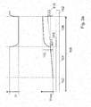
- the CSA operation can be divided in three phases as illustrated in figure 3a .
- the noise source 310 is modelled as a constant DC current.
- the change of C xy capacitance is converted into a voltage through the CSA output ( V CSA ).
- the reset period 102 corresponds to the reset switch 352 being closed, allowing V CSA to equal the reference voltage V bias (the offset being here neglected).
- the boundary between the noise integration period 104, and the voltage sampling period 106 is marked by a transition of the input drive level V r between two different constant values.
- V CSA reacts to a change in the driving voltage V r with a signal proportional to the charge transferred to its input, the gain being nominally equal to -C xy / C fb .
- the noise current 310 contributes to the output with a constant slope ramp when the reset switch is open, and is the origin of the steps ⁇ V 1 and ⁇ V 2 .
- the difference value 110 is given by ( V High - V low ) ⁇ C xy / C fb + ( ⁇ V 1 + ⁇ V 2 ), where ( V High - V low ) is the amplitude of the drive voltage V r .
- Fig. 3b illustrates a known method of correcting the noise error ( ⁇ V 1 + ⁇ V 2 ).
- the voltage acquisition cycle includes two opposite transitions of the driving signal V r and a sampling and holding scheme is in charge of generating two signals, V sh 1 and V sh 2 that store the sampled value of the V_csa output for the first and second part of the acquisition phase respectively.
- V sh 1 and V sh 2 that store the sampled value of the V_csa output for the first and second part of the acquisition phase respectively.
- the difference between the two sampled and held signals V sh 1 and V sh 2 does not contain the DC and low frequency noise contributors anymore.
- the sign change in the driving signal gives rise to useful signals which are in phase opposition on V sh 1 and V sh 2 such that the difference between the two variables exhibits a 6dB gain with respect to the capacitance variation.
- the above method and circuit provide satisfactory elimination of DC offsets and low frequency noise (e.g. 1/f noise or noise coming from the mains).
- High frequency noise can be effectively mitigated by low-pass filter 40, or equivalent signal processing techniques.
- US20080204040 describes an electronic interface for reading a capacitive sensor that includes an input capacitor whose capacitance Cx depends from a value to be measured. This electronic interface allows to generate an expression for the variable capacitance Cx independent of a number of output error sources, by performing four measurement at an electrode of the input capacitor.
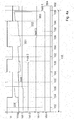
- V CSA in an aspect of the present invention four consecutive samples of V CSA are generated corresponding to positive, negative, negative then positive integration respectively V sh 1 , V sh 2 , V sh 3 and V sh 4 .
- the wording 'positive integration' and 'negative integration' refers to the polarity of the signal present on V CSA and, to the values of the drive excitation voltage V f .
- the drive voltage V f can assume two values, V low and V high : when V f switches from V high to V low , a negative charge ( V low - V high ) ⁇ C xy is injected at the input of the charge-sense amplifier 35, and the output V CSA exhibits a positive step; conversely, the transition of V f from V low to V high corresponds to a negative V CSA step.
- the invention could also rely on the complementary logic, and take four samples corresponding to negative, positive, positive and then again negative integration.
- the samples V sh 1 , V sh 2 , V sh 3 and V sh 4 could include two samples corresponding to V low and two samples corresponding to V high in a different order.
- the output V CSA is reset (periods 102) to a predetermined reference value after the sampling of V sh 1 , V sh 2 , V sh 3 and V sh 4 .
- Vsh p nT Vbias + U + ⁇ ⁇ n n ⁇ 1 T + Tr ⁇ nT T ⁇ Tr Cfb
- Vsh p nT Vbias + U + ⁇ n ⁇ 1 T + Tr nT i n t dt Cfb
- Vsh p nT Vbias + U ⁇ ⁇ T 2 + Tr 2 2 + T . Tr . n ⁇ 1 ⁇ nT 2 Cfb
- Vsh p n ⁇ 4 T Vbias + U ⁇ ⁇ 9 T 2 + Tr 2 2 + T . Tr . n ⁇ 5 ⁇ nT 2 Cfb
- Vsh n n + 1 T Vbias ⁇ U ⁇ ⁇ T r 2 ⁇ T 2 2 + T . Tr . n ⁇ nT 2 Cfb
- Vsh n n ⁇ 3 T Vbias ⁇ U ⁇ ⁇ 7 T 2 + Tr 2 2 + T . Tr . n ⁇ 4 ⁇ nT 2 Cfb
- Vd n n + 1 T 4 ⁇ ⁇ T 2 ⁇ T . Tr Cfb
- V 12 V sh 1 - V sh 2 , as the difference between two S/H outputs corresponding to different values of the drive excitation voltage V f .
- V 12 V sh 1 - V sh 2 , will be a square wave of peak to peak value as defined by Vd p and Vd n , of period 4 ⁇ T and mean value of 2 ⁇ U as Fig. 4b and 5a illustrate.
- Vd n n + 2 T 4 ⁇ ⁇ T 2 ⁇ T ⁇ Tr Cfb
- Vd p n + 3 T 4 ⁇ ⁇ T 2 ⁇ T ⁇ Tr Cfb
- Fig 6 represents, in function of time, a noise current signal 310 comprising a low-frequency sine wave component that represents for example a noise at mains frequency with superimposed triangle noise spikes as coming from a switched power supply or a backlight panel, or lamps, for example, and the corresponding V comp signal 650.
- a noise current signal 310 comprising a low-frequency sine wave component that represents for example a noise at mains frequency with superimposed triangle noise spikes as coming from a switched power supply or a backlight panel, or lamps, for example, and the corresponding V comp signal 650.
- the V comp signal exhibits a 0V mean value with square waves and pulses corresponding to the incoming noise current.
- the peak to peak amplitudes are proportional to its first derivative as explained in the beginning of this section.
- the V comp samples no longer exhibit constant amplitude square waves but rather several larger amplitudes spikes, corresponding to the high involved noise di n / dt.
- the composite signal V comp can be considered as a reference level for medium frequency noise detection and elimination.
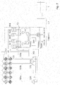
- FIG. 7 shows the block diagram for one column of a possible implementation of the proposed system. It includes a XY array of electrodes connected together in columns 130, and rows 120a-120k. The rows are connected each to a row driver 32a-32k having an analogous function to the driver 32 of Fig. 2 .
- the columns, (of which only one is represented for clarity's sake) are coupled to a readout circuit including a charge-sense amplifier 35 as in Fig. 2 , and four sample/hold circuits 501, 502, 503, 504.
- a timing circuit 300 generates the necessary timing signals to enable the row drivers 32a-32k sequentially in a scanning cycle 109, and also commands the reset of the CSA 35 and triggers the operation of the sample/hold circuits 501, 502, 503, 504. The timing is illustrated by Fig. 8 .
- the evaluation unit further generates an analogue signal V out_raw proportional to the charge transferred to the input of the charge-sense amplifier.
- V out _ raw is fed to an ADC 80 that generates a (M+1) bit word V out_raw [M: 0].
- V out _ raw V12 + V34 which provides a gain of 4 (12dB) with respect to the useful signal.
- the samples V sh 1 , V sh 2 , V sh 3 and V sh 4 contribute to V out_raw with weights equal to +1 for the positive samples V sh 1 and V sh 3 and to -1 for the negative samples V sh 2 and V sh 4 .
- the sample-and-hold 501, 502, 503, 504 are operationally arranged to hold four samples V sh 1 , V sh 2 , V sh 3 , V sh 4 of the output of the charge-sense amplifier 35.
- the output of V csa is digitized by a single sample-and-hold and ADC circuit, timed to sample and acquire the four samples V sh 1 , V sh 2 , V sh 3 , V sh 4 serially.
- a discriminator block 330 is in charge of generating a digital flag (error_bit), each time the magnitude of V comp has overcome a pre-defined threshold, thereby indicating that the value of signal V out_raw is affected by a current noise exceeding a certain slope ( di n / dt ).
Landscapes
- Engineering & Computer Science (AREA)
- General Engineering & Computer Science (AREA)
- Theoretical Computer Science (AREA)
- Human Computer Interaction (AREA)
- Physics & Mathematics (AREA)
- General Physics & Mathematics (AREA)
- Position Input By Displaying (AREA)
Description
- The present invention concerns electronic capacity sensor and in particular, but not exclusively, devices that detect a variation in the capacitive couplings among an array of electrodes.
- Embodiments of the present invention relate to touch-sensitive screens, track pads, and touch-sensitive input devices for computers.
- Other embodiments of the invention relate to the use of capacitive sensors in other applications like proximity sensors, MEMS devices, accelerometers, position encoders and any application requesting to interface with capacitive sensors, and particularly to scan multiple capacitive sensors.
- Aspects of the invention are an electric filter and the corresponding signal processing method used to extract inter-electrode capacity variations from an array of electrodes rejecting ambient electromagnetic noise.
- The circuits of
Fig. 1 and 2 are used in a variety of application fields that must sense minute capacity changes. Theinput capacitor 30, which may be realized by any suitable electrode arrangement, is connected between a constant potential (the ground in this case) and the input of a charge-sense amplifier 35. The input of theamplifier 35 is a virtual ground point, the feedback loop being arranged to keep its potential constant. The output of theamplifier 35 can be forced to a suitable reference value Vinit by a reset circuit, represented by theswitch 352 inFig. 2 . After the reset, the output voltage will reflect the value of theinput capacitor 30 according to the formula VCSA = Vinit - Q/Cf where Cf is the value of thefeedback capacitor 335 and Q is the transferred charge. Any change in the charges stored into the sensing capacitor, resulting from a capacitance change for instance, will be seen as a voltage change at the output of the integrator. Various implementation schemes of the integrator stage are known in the art. - The
block 40 is a low pass filter. Its purpose is to remove high frequency noise components from the measurement without significantly attenuating the transferred signal. Theblock 50 is a track and hold or a sample and hold circuit. It is required to store the result of the integrator at the end of the charge transfer phase and keep it available for the whole duration of the A/D conversion carried out in theADC 80, in order to allow a new charge to be sampled while the current one is being converted. -
Figure 2 represents a readout circuit of a capacitive cell of a XY capacitive sensor matrix, as it could be integrated into a touch screen, a track pad, or any other suitable device. Theinput capacitor 30 represents the capacitance existing between arow 130 and acolumn 120 of electrodes that can be modified by an approaching finger, for example. Thedriver 32 applies a square pulse Vr of determined amplitude to theelectrodes 30 of each line (or column) of the matrix in order to inject a predetermined reference charge on the rising and falling edges of the pulses. The pulses can also be timed, as it will be seen further on, in order to interrogate sequentially the lines of the matrix. - The reference charges, also called reference charges without touch (QNT ) are detected by the charge-
sense amplifier 35 which amplifies and converts them in a voltage signal. The amount of charges is proportional to the mutual capacitance Cxy between the X and Y electrodes of each coplanar capacitor of the projected capacitive matrix. When the user finger is close to the matrix surface, the coupled surface electric field of the coplanar capacitor will be modified, inducing a change of the mutual capacitance value Cxy, thus changing the coupled charges between the X and Y electrodes of the capacitor(s) located under the finger. The new amount of charges with touch, called QT, is detected and amplified during a new scan pulse. The difference between QNT and QT is the sampled touch signal which can be processed and converted. In a non-ideal real case, the output VCSA of the charge-sense amplifier will be affected not only by the user's finger, but also by environmental and intrinsic noise, represented by thecurrent source 310. Noise introduces an error on the absolute VCSA level and can lead to various system errors. In the important case of capacitive touch application, false touches can be triggered by noise, depending on its level amplitude and spectral characteristics. - The CSA operation can be divided in three phases as illustrated in
figure 3a . In this example, for simplicity, thenoise source 310 is modelled as a constant DC current. The change of Cxy capacitance is converted into a voltage through the CSA output (VCSA ). Thereset period 102 corresponds to thereset switch 352 being closed, allowing VCSA to equal the reference voltage Vbias (the offset being here neglected). The boundary between thenoise integration period 104, and thevoltage sampling period 106 is marked by a transition of the input drive level Vr between two different constant values. In an ideal case where there is no leakage or noise current on Vc , the total charge being conserved the output VCSA reacts to a change in the driving voltage Vr with a signal proportional to the charge transferred to its input, the gain being nominally equal to -Cxy /Cfb. - In the example of
Fig. 3a , thenoise current 310 contributes to the output with a constant slope ramp when the reset switch is open, and is the origin of the steps ΔV 1 and ΔV 2. Thedifference value 110 is given by (VHigh - Vlow ) · Cxy /Cfb + (ΔV 1 + ΔV 2), where (VHigh - Vlow ) is the amplitude of the drive voltage Vr . -
Fig. 3b illustrates a known method of correcting the noise error (ΔV 1 + ΔV 2). The voltage acquisition cycle includes two opposite transitions of the driving signal Vr and a sampling and holding scheme is in charge of generating two signals, V sh1 and V sh2 that store the sampled value of the V_csa output for the first and second part of the acquisition phase respectively. Assuming a good correlation of the noise contribution in between two consecutive samples, the difference between the two sampled and held signals V sh1 and V sh2 does not contain the DC and low frequency noise contributors anymore. In addition, when a real capacitive change occurs, the sign change in the driving signal gives rise to useful signals which are in phase opposition on V sh1 and V sh2 such that the difference between the two variables exhibits a 6dB gain with respect to the capacitance variation. - The above method and circuit provide satisfactory elimination of DC offsets and low frequency noise (e.g. 1/f noise or noise coming from the mains). High frequency noise, on the other hand, can be effectively mitigated by low-
pass filter 40, or equivalent signal processing techniques. - Known circuits, for example those disclosed in documents
US2011163768 andUS2011102061 , still have unsatisfactory rejection of for medium frequency noise events such that coming from switching devices such as power supplies, lighting lamps and backlights, in particular if the noise between two consecutive samples is uncorrelated. -
US20080204040 describes an electronic interface for reading a capacitive sensor that includes an input capacitor whose capacitance Cx depends from a value to be measured. This electronic interface allows to generate an expression for the variable capacitance Cx independent of a number of output error sources, by performing four measurement at an electrode of the input capacitor. - It is therefore an aim of the present invention to provide a novel capacitive touch sensor circuit, as well as the corresponding filter and processing method that can extract a signal from a capacitive sensor and has a better immunity to noise.
- According to the invention, these aims are achieved by means of the objects of the appended claims.
- The invention will be better understood with the aid of the description of an embodiment given by way of example and illustrated by the figures, in which:
-
Fig. 1 shows schematically a generic capacitive sensor readout. -
Fig. 2 represents an array of capacitive sensors and the corresponding readout circuitry. -
Fig. 3a and3b illustrate schematically the principal electric signals of the circuit offigure 2 , including the effect of low-frequency noise, and an alternate sampling scheme. -
Fig. 4a and4b show the readout cycle of a sampling scheme according to an aspect of the invention. -
Fig. 5a and 5b illustrate other signals used in various embodiments of the invention. -
Fig. 6 relates to a situation including several sources of environment noise. -
Fig. 7 illustrates schematically a touch sensitive capacitive array device according to an aspect of the present invention. -
Fig. 8 relates to the organization of a scanning cycle in the device illustrated inFig. 7 . -
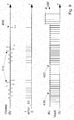
Fig. 9 shows the data format and error-signal flags generated by the circuit offig. 7 . -
Fig. 10 shows an example of performance of an embodiment of the present invention in presence of various noise sources. - Referring now to
fig. 4a , in an aspect of the present invention four consecutive samples of VCSA are generated corresponding to positive, negative, negative then positive integration respectively V sh1, V sh2, V sh3 and V sh4. The wording 'positive integration' and 'negative integration' refers to the polarity of the signal present on VCSA and, to the values of the drive excitation voltage Vf. Let's assume for example that the drive voltage Vf can assume two values, Vlow and Vhigh : when Vf switches from Vhigh to Vlow, a negative charge (Vlow - Vhigh ) · Cxy is injected at the input of the charge-sense amplifier 35, and the output VCSA exhibits a positive step; conversely, the transition of Vf from Vlow to Vhigh corresponds to a negative VCSA step. The invention, however, could also rely on the complementary logic, and take four samples corresponding to negative, positive, positive and then again negative integration. In a generalization, the samples V sh1, V sh2, V sh3 and V sh4 could include two samples corresponding to Vlow and two samples corresponding to Vhigh in a different order. According to an important aspect of the invention, the output VCSA is reset (periods 102) to a predetermined reference value after the sampling of V sh1, V sh2, V sh3 and V sh4. - Let's now assume that the sampling frequency Fs = 1/T is sufficiently faster than the Nyquist frequency associated with the incoming noise. Let's call U the useful signal:

Fig. 2 ). We can then write the expression for one S/H output during the nth positive integration period during which it is activated. Noting that during thereset period 102, there is obviously no integration taking place such that the average noise current ĩ n(t) during a period starting at (n-1)T and ending at nT should actually start at ((n - 1) · T + Tr );

- If, for simplification, we assume that the noise current exhibits a linear relationship with respect to time, or more generally if the noise signal can be substituted by its first derivative during at least one quadruple sampling period, preferably during several quadruple sampling periods, we can write:

- We also note from
Fig. 4a that the global period of each of the four SH signals (Vsh1,2,3,4) is 4 · T. Substituting in(t) by its value from equation above, we can find the two consecutive samples from a given S/H output corresponding to a positive integration and finally their difference:


- If now we focus on the (n+1)th sample which corresponds to a negative integration, we can similarly express the difference between the two consecutive samples from the concerned SH output:



- From equations on Vdp and Vdn, we notice that in steady state, the step between two outputs of each SH is constant and independent of the sampling index, it is also proportional to the slope of the incoming noise signal. Let's define now V12 = V sh1 - V sh2, as the difference between two S/H outputs corresponding to different values of the drive excitation voltage Vf. V12 = V sh1 - V sh2, will be a square wave of peak to peak value as defined by Vdp and Vdn, of
period 4 · T and mean value of 2 · U asFig. 4b and5a illustrate. - A similar analysis can be conducted for the two other S/H outputs V sh3 and V sh4. Using the same starting assumptions, we obtain:


- Taking now the difference between these two S/H outputs V34 = V sh3 - V sh4, which also correspond to to different values of the drive excitation voltage Vf, we obtain in steady state a square wave of same peak to peak value as for signal V12, still a mean value of 2 · U but because of the inversion of the integration sign (negative for phase (n+2)T then positive for phase (n+3)T), we can observe a duty cycle of 75% for the case of a positive noise i n(t). This is shown in
Fig. 5a . Clearly in case of negative noise, the signals V12 and V34 would exhibit 75% and 25% duty cycle respectively. - According to an aspect of the present invention, the signal Vcomp = V12 - V34 is generated by combining two square waves defined above in order to obtain a signal proportional to the charge transferred to the input of the charge-sense amplifier (the signal Vcomp is defined as the result of a subtraction but, clearly, if one permutes the terms in the definition of V12 and V23, an addition or a different combination would be needed to arrive at the same algebraic value). Thanks to the alternate integration sign, the steady Vcomp signal during a time linear noise always exhibit a 50% duty cycle pattern centred at 0V. This is shown in
Fig. 5b . -
Fig 6 represents, in function of time, a noisecurrent signal 310 comprising a low-frequency sine wave component that represents for example a noise at mains frequency with superimposed triangle noise spikes as coming from a switched power supply or a backlight panel, or lamps, for example, and the corresponding Vcomp signal 650. - As expected, the Vcomp signal exhibits a 0V mean value with square waves and pulses corresponding to the incoming noise current. When the noise current varies linearly or quasi-linearly with time and when the quadruple S/H system can correctly track the noise, then the peak to peak amplitudes are proportional to its first derivative as explained in the beginning of this section. For fast transients as seen at the end of the noise pulses, the Vcomp samples no longer exhibit constant amplitude square waves but rather several larger amplitudes spikes, corresponding to the high involved noise din /dt.
- Having a well defined average level of 0V affected by bidirectional spikes proportional to noise din /dt, the composite signal Vcomp can be considered as a reference level for medium frequency noise detection and elimination.
- In an actual touch panel system, "L" Charge Sensing Amplifiers are hooked to "L" columns which intersect with "K" rows.
Figure 7 shows the block diagram for one column of a possible implementation of the proposed system. It includes a XY array of electrodes connected together incolumns 130, androws 120a-120k. The rows are connected each to a row driver 32a-32k having an analogous function to thedriver 32 ofFig. 2 . The columns, (of which only one is represented for clarity's sake) are coupled to a readout circuit including a charge-sense amplifier 35 as inFig. 2 , and four sample/hold circuits timing circuit 300 generates the necessary timing signals to enable the row drivers 32a-32k sequentially in ascanning cycle 109, and also commands the reset of theCSA 35 and triggers the operation of the sample/hold circuits Fig. 8 . - The
evaluation unit 333 generates through addition and subtraction of the four outputs of the sample/hold circuits, the functions V12, V34 and Vcomp = V12 - V34 as explained above. The evaluation unit further generates an analogue signal Vout_raw proportional to the charge transferred to the input of the charge-sense amplifier. V out_raw is fed to anADC 80 that generates a (M+1) bit word Vout_raw [M: 0]. In the presented example V out_raw = V12 + V34 which provides a gain of 4 (12dB) with respect to the useful signal. The samples V sh1, V sh2, V sh3 and V sh4 contribute to Vout_raw with weights equal to +1 for the positive samples V sh1 and V sh3 and to -1 for the negative samples V sh2 and V sh4. - According to the particular embodiment represented schematically in
Fig. 7 , the sample-and-hold sense amplifier 35. It must be understood, however, that the present invention is not limited to the case of four physically separate sample-and-hold, and that the same could be obtained by a lower number of time-multiplexed units. In a particularly simple realization, the output of Vcsa is digitized by a single sample-and-hold and ADC circuit, timed to sample and acquire the four samples V sh1, V sh2, V sh3, V sh4 serially. The evaluation of Vcomp = V12 - V34 and Vout_raw = V12 + V34 is then carried out on the digital values by a hardwired logic circuit, or by a DSP. - A
discriminator block 330 is in charge of generating a digital flag (error_bit), each time the magnitude of Vcomp has overcome a pre-defined threshold, thereby indicating that the value of signal Vout_raw is affected by a current noise exceeding a certain slope (din /dt). - According to a variant of the invention, the system could include a parallel ADC arranged to convert Vcomp = V12 - V34 in noise samples which are a representation of the noise (din /dt), while Vout_raw , digitized by the
main ADC 80, provides a digital representation of signal + noise. Further signal processing can be used to obtain a noise-subtracted signal. Equivalently, the system could include two ADC arranged to convert the signals V12 = V sh1 - V sh2 and V34 = V sh3 - V sh4, from which the signal and the noise are obtained arithmetically, as seen above. - Once the samples impacted by noise have been identified thanks to the error_bit digital flag, further processing can take place to eliminate and/or replace the concerned converted samples from V out_raw in order to obtain the output signal Vout. Several techniques are possible, placing more or less constraints on the digital processing. In
Fig. 9 , a straight replacement of missing samples by a default value is shown. This straight substitution approach is effective and is simple to implement, but signal drops 470 visible inFig. 10 can be introduced if noise pulses occur during the touch itself. In many significant applications where the capacitive touch sensor is actually a 2D device, the effect of these drops can be mitigated by known digital image processing techniques like in-painting for example.
Claims (13)
- Electronic interface for reading a capacitive sensor that includes one input capacitor (30) or several input capacitors whose capacitance depends from a value that must be measured,
the interface including at least one driver (32, 32a-k) generating an electric excitation voltage that varies between a first voltage level (Vlow) and a second voltage level (Vhigh) connected to one electrode of the input capacitor (30), characterized by
a charge-sense amplifier connected to another electrode of the input capacitor (30) and arranged to output a signal (VCSA, 358) proportional to the charge transferred to the input of the charge-sense amplifier, sampling means (501, 502, 503, 504) operationally arranged to hold four samples (V sh1, V sh2, V sh3, V sh4) of the output of the charge-sense amplifier,
a timing circuit (300) determining the instants of said four samples and the excitation voltage generated by said driver (32, 32a-k) such that two of said four samples (V sh2, V sh3) are generated when the electric excitation voltage is at said first voltage level (Vlow ), while the two other samples (V sh1 , V sh4) are generated when the electric excitation voltage is at said second voltage level (Vhigh ). - The electronic interface circuit of the previous claim, further characterized by an evaluation unit (333) arranged to compute two difference values (V12, V34) between two pairs of samples corresponding to different voltage levels and to combine said difference values into an output value (Vout_raw ) proportional to the charge transferred to the input of the charge-sense amplifier.
- The electronic interface circuit of the previous claim, wherein the evaluation unit is further arranged to combine said difference values into an error value (error_bit) sensitive to a time derivative of a noise current (din /dt).
- The electronic interface circuit of the previous claim, wherein the error value identifies samples impacted by noise.
- The electronic interface circuit of any of the previous claims, in which the charge-sensitive amplifier includes as well reset means (352) arranged to force the output (VCSA ) of the charge-sensitive amplifier (35) to a determined reference value (Vinit ).
- Combination of the electronic interface circuit of any of the previous claims, with a capacitive touch sensitive device comprising a plurality of input capacitors organized in rows and columns to form a 2D array, the electronic interface circuit being arranged to scan the capacitors and provide signals indicative of the position of one or more fingers touching the touch sensitive device.
- The combination of the previous claim, wherein the electronic interface circuit comprises an evaluation unit (333) arranged to compute two difference values (V12, V34) between two pairs of samples corresponding to different voltage levels and to combine said difference values into an output value (Vout_raw ) proportional to the charge transferred to the input of the charge-sense amplifier, and into an error value (error_bit) sensitive to a time derivative of a noise current (din /dt), wherein the error value identifies samples impacted by noise, and comprising a digital processor arranged to replace the samples impacted by noise by a predetermined default value.
- The combination of the previous claim, further comprising a digital image processor.
- Method of reading a capacitive sensor (30), comprising:
applying an electric excitation voltage that varies between a first voltage level (Vlow ) and a second voltage level (Vhigh ) connected to one electrode of the capacitive sensor (30), reading the charge transmitted by the capacitive sensor (30) by a charge-sense amplifier connected to another electrode of the capacitive sensor (30), collecting four samples (V sh1, V sh2, V sh3, V sh4) of the output of the charge-sense amplifier at instants determined such that two of said four samples (V sh2 ,V sh3) are generated when the electric excitation voltage is at said first voltage level (Vlow ), while the two other samples (V sh1, V sh4) are generated when the electric excitation voltage is at said second voltage level (Vhigh ). - The method of the previous claim, comprising a step of computing two difference values (V12, V34) between two pairs of samples corresponding to different voltage levels and combining said difference values into an output value (Vout_raw ) proportional to the charge transferred to the input of the charge-sense amplifier.
- The method of the previous claim, comprising combining said difference values into an error value (error_bit) sensitive to a time derivative of a noise current (din /dt).
- The method of the previous claim, comprising identifying samples impacted by the noise based on said error value.
- Use of the method of any of claims 9 to 12 in reading a capacitive touch sensitive device comprising a plurality of input capacitors organized in rows and columns to form a 2D array.
Applications Claiming Priority (2)
| Application Number | Priority Date | Filing Date | Title |
|---|---|---|---|
| CH01916/11A CH705869A1 (en) | 2011-12-02 | 2011-12-02 | Interface and capacitive sensor reading method. |
| PCT/EP2012/067239 WO2013079232A1 (en) | 2011-12-02 | 2012-09-04 | Capacitive sensor interface and method |
Publications (2)
| Publication Number | Publication Date |
|---|---|
| EP2786489A1 EP2786489A1 (en) | 2014-10-08 |
| EP2786489B1 true EP2786489B1 (en) | 2019-11-06 |
Family
ID=46796610
Family Applications (1)
| Application Number | Title | Priority Date | Filing Date |
|---|---|---|---|
| EP12753997.1A Active EP2786489B1 (en) | 2011-12-02 | 2012-09-04 | Capacitive sensor interface and method |
Country Status (8)
| Country | Link |
|---|---|
| US (1) | US9214938B2 (en) |
| EP (1) | EP2786489B1 (en) |
| JP (1) | JP2015501038A (en) |
| KR (1) | KR20140106586A (en) |
| CN (1) | CN103959650A (en) |
| CH (1) | CH705869A1 (en) |
| TW (1) | TWI450175B (en) |
| WO (1) | WO2013079232A1 (en) |
Families Citing this family (17)
| Publication number | Priority date | Publication date | Assignee | Title |
|---|---|---|---|---|
| KR102014276B1 (en) * | 2012-11-12 | 2019-08-26 | 엘지디스플레이 주식회사 | Display device and driving method thereof |
| KR20150057652A (en) * | 2013-11-20 | 2015-05-28 | 삼성전기주식회사 | Touchscreen apparatus and driving method thereof |
| KR101635134B1 (en) * | 2014-07-08 | 2016-06-30 | 주식회사 동부하이텍 | A touch sensor |
| KR102249651B1 (en) | 2014-07-23 | 2021-05-10 | 주식회사 실리콘웍스 | Touch panel sensing apparatus and controlling apparatus thereof |
| TWI575430B (en) * | 2014-12-17 | 2017-03-21 | 速博思股份有限公司 | Mutual-capacitance input device with hovering touch |
| US10325131B2 (en) * | 2015-06-30 | 2019-06-18 | Synaptics Incorporated | Active matrix capacitive fingerprint sensor for display integration based on charge sensing by a 2-TFT pixel architecture |
| WO2017003848A1 (en) * | 2015-06-30 | 2017-01-05 | Synaptics Incorporated | Active matrix capacitive fingerprint sensor with 1-tft pixel architecture for display integration |
| DE102015008485A1 (en) * | 2015-07-01 | 2017-01-05 | Leopold Kostal Gmbh & Co. Kg | Method for measuring a capacitance value |
| US9817530B2 (en) | 2015-08-31 | 2017-11-14 | Stmicroelectronics Asia Pacific Pte. Ltd. | Electronic device with touchscreen for removing sample subsets and related methods |
| TWI569185B (en) | 2015-11-06 | 2017-02-01 | 財團法人工業技術研究院 | Touch control apparatus and noise compensating circuit and method thereof |
| US9600707B1 (en) | 2015-11-30 | 2017-03-21 | Fingerprint Cards Ab | Analog sampling system and method for noise supression |
| US9983246B2 (en) * | 2016-01-15 | 2018-05-29 | Cypress Semiconductor Corporation | Quasi-differential mutual capacitance measurement |
| TWI627619B (en) | 2017-11-28 | 2018-06-21 | Industrial Technology Research Institute | Touch panel driving apparatus |
| TWI640778B (en) | 2018-03-02 | 2018-11-11 | National Applied Research Laboratories | Signal error calibrating method |
| TWI779534B (en) * | 2020-03-25 | 2022-10-01 | 昇佳電子股份有限公司 | Capacitance sensing circuit |
| CN114124066B (en) * | 2020-08-26 | 2024-07-02 | 浙江智识电子科技有限公司 | Environment slowly-changing self-adaptive capacitance induction detection system |
| CN117825748B (en) * | 2024-03-01 | 2024-05-28 | 华中科技大学 | Static accelerometer for reducing 1/f noise of readout circuit based on in-loop double modulation |
Family Cites Families (11)
| Publication number | Priority date | Publication date | Assignee | Title |
|---|---|---|---|---|
| US6452514B1 (en) * | 1999-01-26 | 2002-09-17 | Harald Philipp | Capacitive sensor and array |
| US7643011B2 (en) * | 2007-01-03 | 2010-01-05 | Apple Inc. | Noise detection in multi-touch sensors |
| US7592819B2 (en) * | 2007-02-23 | 2009-09-22 | Sensata Technologies, Inc. | Microprocessor-based capacitance measurement |
| JP4872113B2 (en) * | 2007-09-10 | 2012-02-08 | 株式会社ワコム | Position detection device |
| US8314779B2 (en) * | 2009-02-23 | 2012-11-20 | Solomon Systech Limited | Method and apparatus for operating a touch panel |
| JP5178633B2 (en) * | 2009-05-29 | 2013-04-10 | 株式会社ジャパンディスプレイウェスト | Touch sensor, display device, and electronic device |
| TWI397843B (en) * | 2009-10-30 | 2013-06-01 | Orise Technology Co Ltd | Touch panel sensing circuit |
| US20110163768A1 (en) * | 2010-01-05 | 2011-07-07 | Sain Infocom | Touch screen device, capacitance measuring circuit thereof, and method of measuring capacitance |
| EP2541378A1 (en) * | 2010-04-01 | 2013-01-02 | Sharp Kabushiki Kaisha | Display device with touch sensor |
| US8274491B2 (en) * | 2010-06-21 | 2012-09-25 | Pixart Imaging Inc. | Capacitive touchscreen signal acquisition without panel reset |
| WO2012034714A1 (en) * | 2010-09-14 | 2012-03-22 | Advanced Silicon Sa | Circuit for capacitive touch applications |
-
2011
- 2011-12-02 CH CH01916/11A patent/CH705869A1/en not_active Application Discontinuation
-
2012
- 2012-09-04 WO PCT/EP2012/067239 patent/WO2013079232A1/en not_active Ceased
- 2012-09-04 CN CN201280059498.8A patent/CN103959650A/en active Pending
- 2012-09-04 EP EP12753997.1A patent/EP2786489B1/en active Active
- 2012-09-04 JP JP2014543811A patent/JP2015501038A/en active Pending
- 2012-09-04 KR KR1020147016837A patent/KR20140106586A/en not_active Withdrawn
- 2012-11-09 TW TW101141762A patent/TWI450175B/en active
- 2012-11-27 US US13/686,286 patent/US9214938B2/en active Active
Non-Patent Citations (1)
| Title |
|---|
| None * |
Also Published As
| Publication number | Publication date |
|---|---|
| CH705869A1 (en) | 2013-06-14 |
| TWI450175B (en) | 2014-08-21 |
| TW201331808A (en) | 2013-08-01 |
| US20130141139A1 (en) | 2013-06-06 |
| WO2013079232A1 (en) | 2013-06-06 |
| JP2015501038A (en) | 2015-01-08 |
| KR20140106586A (en) | 2014-09-03 |
| US9214938B2 (en) | 2015-12-15 |
| EP2786489A1 (en) | 2014-10-08 |
| CN103959650A (en) | 2014-07-30 |
Similar Documents
| Publication | Publication Date | Title |
|---|---|---|
| US9214938B2 (en) | Capacitive sensor interface and method | |
| US8928622B2 (en) | Demodulation method and system with low common noise and high SNR for a low-power differential sensing capacitive touch panel | |
| KR101304195B1 (en) | Capacitance sensor with improved noise filtering chracteristics, method and computer-readable recording medium for noise filtering of capacitance sensor | |
| US8860437B2 (en) | Readout system for MEMS-based capacitive accelerometers and strain sensors, and method for reading | |
| US9244569B2 (en) | Capacitive sensing analog front end | |
| CN104965627B (en) | Touch detection circuit and semiconductor integrated circuit provided with same | |
| US8860432B2 (en) | Background noise measurement and frequency selection in touch panel sensor systems | |
| KR101903810B1 (en) | Reduction of noise in touch sensors | |
| US9417739B2 (en) | High speed multi-touch touch device and controller therefor | |
| US8274491B2 (en) | Capacitive touchscreen signal acquisition without panel reset | |
| CN102207804B (en) | Capacitive sensing analog front end | |
| US8681110B2 (en) | Sensing circuit for use with capacitive touch panel | |
| US9692439B2 (en) | Apparatus using a differential analog-to-digital converter | |
| KR102801238B1 (en) | Amplified charge cancellation in touch sensors, and related systems, methods and devices | |
| JP4970129B2 (en) | Proximity detection sensor and proximity detection method | |
| JP5952398B2 (en) | Method and apparatus for sensing and scanning capacitive touch panels | |
| CN107193429B (en) | Touch sensing high-low drive scheme for in-cell touch LCD displays | |
| US20150234017A1 (en) | Magnetic field detecting device | |
| US8593432B2 (en) | Sample and hold analog front end for a capacitive touchpad | |
| KR101209114B1 (en) | Apparatus for sensing charge of touch panel with removing low frequency noise | |
| KR20140066599A (en) | Touch sensing apparatus | |
| KR101307791B1 (en) | CAPACITIVE TOUCH DETECT SYSTEM having improved sensibility | |
| Kim et al. | 45.2: A Capacitive Touchscreen Controller IC with Noise‐based Hybrid Sensing Scheme | |
| Kim et al. | An analog front-end for self-capacitance touch sensing with environmental noise reduction technique |
Legal Events
| Date | Code | Title | Description |
|---|---|---|---|
| PUAI | Public reference made under article 153(3) epc to a published international application that has entered the european phase |
Free format text: ORIGINAL CODE: 0009012 |
|
| 17P | Request for examination filed |
Effective date: 20140520 |
|
| AK | Designated contracting states |
Kind code of ref document: A1 Designated state(s): AL AT BE BG CH CY CZ DE DK EE ES FI FR GB GR HR HU IE IS IT LI LT LU LV MC MK MT NL NO PL PT RO RS SE SI SK SM TR |
|
| DAX | Request for extension of the european patent (deleted) | ||
| RAP1 | Party data changed (applicant data changed or rights of an application transferred) |
Owner name: ADVANCED SILICON SA |
|
| STAA | Information on the status of an ep patent application or granted ep patent |
Free format text: STATUS: EXAMINATION IS IN PROGRESS |
|
| 17Q | First examination report despatched |
Effective date: 20181112 |
|
| GRAP | Despatch of communication of intention to grant a patent |
Free format text: ORIGINAL CODE: EPIDOSNIGR1 |
|
| STAA | Information on the status of an ep patent application or granted ep patent |
Free format text: STATUS: GRANT OF PATENT IS INTENDED |
|
| RIC1 | Information provided on ipc code assigned before grant |
Ipc: H03K 17/96 20060101ALI20190320BHEP Ipc: G06F 3/044 20060101ALI20190320BHEP Ipc: H03K 17/955 20060101AFI20190320BHEP Ipc: G06F 3/041 20060101ALI20190320BHEP |
|
| INTG | Intention to grant announced |
Effective date: 20190411 |
|
| GRAJ | Information related to disapproval of communication of intention to grant by the applicant or resumption of examination proceedings by the epo deleted |
Free format text: ORIGINAL CODE: EPIDOSDIGR1 |
|
| STAA | Information on the status of an ep patent application or granted ep patent |
Free format text: STATUS: EXAMINATION IS IN PROGRESS |
|
| GRAR | Information related to intention to grant a patent recorded |
Free format text: ORIGINAL CODE: EPIDOSNIGR71 |
|
| GRAS | Grant fee paid |
Free format text: ORIGINAL CODE: EPIDOSNIGR3 |
|
| STAA | Information on the status of an ep patent application or granted ep patent |
Free format text: STATUS: GRANT OF PATENT IS INTENDED |
|
| INTC | Intention to grant announced (deleted) | ||
| INTG | Intention to grant announced |
Effective date: 20190827 |
|
| GRAA | (expected) grant |
Free format text: ORIGINAL CODE: 0009210 |
|
| STAA | Information on the status of an ep patent application or granted ep patent |
Free format text: STATUS: THE PATENT HAS BEEN GRANTED |
|
| AK | Designated contracting states |
Kind code of ref document: B1 Designated state(s): AL AT BE BG CH CY CZ DE DK EE ES FI FR GB GR HR HU IE IS IT LI LT LU LV MC MK MT NL NO PL PT RO RS SE SI SK SM TR |
|
| REG | Reference to a national code |
Ref country code: GB Ref legal event code: FG4D |
|
| REG | Reference to a national code |
Ref country code: CH Ref legal event code: EP Ref country code: AT Ref legal event code: REF Ref document number: 1200187 Country of ref document: AT Kind code of ref document: T Effective date: 20191115 |
|
| REG | Reference to a national code |
Ref country code: IE Ref legal event code: FG4D |
|
| REG | Reference to a national code |
Ref country code: DE Ref legal event code: R096 Ref document number: 602012065442 Country of ref document: DE |
|
| REG | Reference to a national code |
Ref country code: NL Ref legal event code: MP Effective date: 20191106 |
|
| REG | Reference to a national code |
Ref country code: LT Ref legal event code: MG4D |
|
| PG25 | Lapsed in a contracting state [announced via postgrant information from national office to epo] |
Ref country code: FI Free format text: LAPSE BECAUSE OF FAILURE TO SUBMIT A TRANSLATION OF THE DESCRIPTION OR TO PAY THE FEE WITHIN THE PRESCRIBED TIME-LIMIT Effective date: 20191106 Ref country code: PL Free format text: LAPSE BECAUSE OF FAILURE TO SUBMIT A TRANSLATION OF THE DESCRIPTION OR TO PAY THE FEE WITHIN THE PRESCRIBED TIME-LIMIT Effective date: 20191106 Ref country code: SE Free format text: LAPSE BECAUSE OF FAILURE TO SUBMIT A TRANSLATION OF THE DESCRIPTION OR TO PAY THE FEE WITHIN THE PRESCRIBED TIME-LIMIT Effective date: 20191106 Ref country code: NL Free format text: LAPSE BECAUSE OF FAILURE TO SUBMIT A TRANSLATION OF THE DESCRIPTION OR TO PAY THE FEE WITHIN THE PRESCRIBED TIME-LIMIT Effective date: 20191106 Ref country code: LT Free format text: LAPSE BECAUSE OF FAILURE TO SUBMIT A TRANSLATION OF THE DESCRIPTION OR TO PAY THE FEE WITHIN THE PRESCRIBED TIME-LIMIT Effective date: 20191106 Ref country code: BG Free format text: LAPSE BECAUSE OF FAILURE TO SUBMIT A TRANSLATION OF THE DESCRIPTION OR TO PAY THE FEE WITHIN THE PRESCRIBED TIME-LIMIT Effective date: 20200206 Ref country code: ES Free format text: LAPSE BECAUSE OF FAILURE TO SUBMIT A TRANSLATION OF THE DESCRIPTION OR TO PAY THE FEE WITHIN THE PRESCRIBED TIME-LIMIT Effective date: 20191106 Ref country code: LV Free format text: LAPSE BECAUSE OF FAILURE TO SUBMIT A TRANSLATION OF THE DESCRIPTION OR TO PAY THE FEE WITHIN THE PRESCRIBED TIME-LIMIT Effective date: 20191106 Ref country code: GR Free format text: LAPSE BECAUSE OF FAILURE TO SUBMIT A TRANSLATION OF THE DESCRIPTION OR TO PAY THE FEE WITHIN THE PRESCRIBED TIME-LIMIT Effective date: 20200207 Ref country code: NO Free format text: LAPSE BECAUSE OF FAILURE TO SUBMIT A TRANSLATION OF THE DESCRIPTION OR TO PAY THE FEE WITHIN THE PRESCRIBED TIME-LIMIT Effective date: 20200206 Ref country code: PT Free format text: LAPSE BECAUSE OF FAILURE TO SUBMIT A TRANSLATION OF THE DESCRIPTION OR TO PAY THE FEE WITHIN THE PRESCRIBED TIME-LIMIT Effective date: 20200306 |
|
| PG25 | Lapsed in a contracting state [announced via postgrant information from national office to epo] |
Ref country code: IS Free format text: LAPSE BECAUSE OF FAILURE TO SUBMIT A TRANSLATION OF THE DESCRIPTION OR TO PAY THE FEE WITHIN THE PRESCRIBED TIME-LIMIT Effective date: 20200306 Ref country code: HR Free format text: LAPSE BECAUSE OF FAILURE TO SUBMIT A TRANSLATION OF THE DESCRIPTION OR TO PAY THE FEE WITHIN THE PRESCRIBED TIME-LIMIT Effective date: 20191106 Ref country code: RS Free format text: LAPSE BECAUSE OF FAILURE TO SUBMIT A TRANSLATION OF THE DESCRIPTION OR TO PAY THE FEE WITHIN THE PRESCRIBED TIME-LIMIT Effective date: 20191106 |
|
| PG25 | Lapsed in a contracting state [announced via postgrant information from national office to epo] |
Ref country code: AL Free format text: LAPSE BECAUSE OF FAILURE TO SUBMIT A TRANSLATION OF THE DESCRIPTION OR TO PAY THE FEE WITHIN THE PRESCRIBED TIME-LIMIT Effective date: 20191106 |
|
| PG25 | Lapsed in a contracting state [announced via postgrant information from national office to epo] |
Ref country code: EE Free format text: LAPSE BECAUSE OF FAILURE TO SUBMIT A TRANSLATION OF THE DESCRIPTION OR TO PAY THE FEE WITHIN THE PRESCRIBED TIME-LIMIT Effective date: 20191106 Ref country code: CZ Free format text: LAPSE BECAUSE OF FAILURE TO SUBMIT A TRANSLATION OF THE DESCRIPTION OR TO PAY THE FEE WITHIN THE PRESCRIBED TIME-LIMIT Effective date: 20191106 Ref country code: RO Free format text: LAPSE BECAUSE OF FAILURE TO SUBMIT A TRANSLATION OF THE DESCRIPTION OR TO PAY THE FEE WITHIN THE PRESCRIBED TIME-LIMIT Effective date: 20191106 Ref country code: DK Free format text: LAPSE BECAUSE OF FAILURE TO SUBMIT A TRANSLATION OF THE DESCRIPTION OR TO PAY THE FEE WITHIN THE PRESCRIBED TIME-LIMIT Effective date: 20191106 |
|
| REG | Reference to a national code |
Ref country code: DE Ref legal event code: R097 Ref document number: 602012065442 Country of ref document: DE |
|
| REG | Reference to a national code |
Ref country code: AT Ref legal event code: MK05 Ref document number: 1200187 Country of ref document: AT Kind code of ref document: T Effective date: 20191106 |
|
| PG25 | Lapsed in a contracting state [announced via postgrant information from national office to epo] |
Ref country code: SK Free format text: LAPSE BECAUSE OF FAILURE TO SUBMIT A TRANSLATION OF THE DESCRIPTION OR TO PAY THE FEE WITHIN THE PRESCRIBED TIME-LIMIT Effective date: 20191106 Ref country code: SM Free format text: LAPSE BECAUSE OF FAILURE TO SUBMIT A TRANSLATION OF THE DESCRIPTION OR TO PAY THE FEE WITHIN THE PRESCRIBED TIME-LIMIT Effective date: 20191106 |
|
| PLBE | No opposition filed within time limit |
Free format text: ORIGINAL CODE: 0009261 |
|
| STAA | Information on the status of an ep patent application or granted ep patent |
Free format text: STATUS: NO OPPOSITION FILED WITHIN TIME LIMIT |
|
| 26N | No opposition filed |
Effective date: 20200807 |
|
| PG25 | Lapsed in a contracting state [announced via postgrant information from national office to epo] |
Ref country code: SI Free format text: LAPSE BECAUSE OF FAILURE TO SUBMIT A TRANSLATION OF THE DESCRIPTION OR TO PAY THE FEE WITHIN THE PRESCRIBED TIME-LIMIT Effective date: 20191106 Ref country code: AT Free format text: LAPSE BECAUSE OF FAILURE TO SUBMIT A TRANSLATION OF THE DESCRIPTION OR TO PAY THE FEE WITHIN THE PRESCRIBED TIME-LIMIT Effective date: 20191106 |
|
| PG25 | Lapsed in a contracting state [announced via postgrant information from national office to epo] |
Ref country code: IT Free format text: LAPSE BECAUSE OF FAILURE TO SUBMIT A TRANSLATION OF THE DESCRIPTION OR TO PAY THE FEE WITHIN THE PRESCRIBED TIME-LIMIT Effective date: 20191106 |
|
| PG25 | Lapsed in a contracting state [announced via postgrant information from national office to epo] |
Ref country code: MC Free format text: LAPSE BECAUSE OF FAILURE TO SUBMIT A TRANSLATION OF THE DESCRIPTION OR TO PAY THE FEE WITHIN THE PRESCRIBED TIME-LIMIT Effective date: 20191106 |
|
| REG | Reference to a national code |
Ref country code: CH Ref legal event code: PL |
|
| REG | Reference to a national code |
Ref country code: BE Ref legal event code: MM Effective date: 20200930 |
|
| PG25 | Lapsed in a contracting state [announced via postgrant information from national office to epo] |
Ref country code: LU Free format text: LAPSE BECAUSE OF NON-PAYMENT OF DUE FEES Effective date: 20200904 |
|
| PG25 | Lapsed in a contracting state [announced via postgrant information from national office to epo] |
Ref country code: LI Free format text: LAPSE BECAUSE OF NON-PAYMENT OF DUE FEES Effective date: 20200930 Ref country code: IE Free format text: LAPSE BECAUSE OF NON-PAYMENT OF DUE FEES Effective date: 20200904 Ref country code: CH Free format text: LAPSE BECAUSE OF NON-PAYMENT OF DUE FEES Effective date: 20200930 Ref country code: BE Free format text: LAPSE BECAUSE OF NON-PAYMENT OF DUE FEES Effective date: 20200930 |
|
| PG25 | Lapsed in a contracting state [announced via postgrant information from national office to epo] |
Ref country code: TR Free format text: LAPSE BECAUSE OF FAILURE TO SUBMIT A TRANSLATION OF THE DESCRIPTION OR TO PAY THE FEE WITHIN THE PRESCRIBED TIME-LIMIT Effective date: 20191106 Ref country code: MT Free format text: LAPSE BECAUSE OF FAILURE TO SUBMIT A TRANSLATION OF THE DESCRIPTION OR TO PAY THE FEE WITHIN THE PRESCRIBED TIME-LIMIT Effective date: 20191106 Ref country code: CY Free format text: LAPSE BECAUSE OF FAILURE TO SUBMIT A TRANSLATION OF THE DESCRIPTION OR TO PAY THE FEE WITHIN THE PRESCRIBED TIME-LIMIT Effective date: 20191106 |
|
| PG25 | Lapsed in a contracting state [announced via postgrant information from national office to epo] |
Ref country code: MK Free format text: LAPSE BECAUSE OF FAILURE TO SUBMIT A TRANSLATION OF THE DESCRIPTION OR TO PAY THE FEE WITHIN THE PRESCRIBED TIME-LIMIT Effective date: 20191106 |
|
| PGFP | Annual fee paid to national office [announced via postgrant information from national office to epo] |
Ref country code: DE Payment date: 20250919 Year of fee payment: 14 |
|
| PGFP | Annual fee paid to national office [announced via postgrant information from national office to epo] |
Ref country code: GB Payment date: 20250918 Year of fee payment: 14 |
|
| PGFP | Annual fee paid to national office [announced via postgrant information from national office to epo] |
Ref country code: FR Payment date: 20250922 Year of fee payment: 14 |