EP2784938B1 - Synchronous input signal capture system - Google Patents
Synchronous input signal capture system Download PDFInfo
- Publication number
- EP2784938B1 EP2784938B1 EP14161767.0A EP14161767A EP2784938B1 EP 2784938 B1 EP2784938 B1 EP 2784938B1 EP 14161767 A EP14161767 A EP 14161767A EP 2784938 B1 EP2784938 B1 EP 2784938B1
- Authority
- EP
- European Patent Office
- Prior art keywords
- signal
- control signal
- logic
- input
- flop
- Prior art date
- Legal status (The legal status is an assumption and is not a legal conclusion. Google has not performed a legal analysis and makes no representation as to the accuracy of the status listed.)
- Active
Links
Images

Classifications
-
- H—ELECTRICITY
- H03—ELECTRONIC CIRCUITRY
- H03K—PULSE TECHNIQUE
- H03K19/00—Logic circuits, i.e. having at least two inputs acting on one output; Inverting circuits
- H03K19/003—Modifications for increasing the reliability for protection
-
- H—ELECTRICITY
- H03—ELECTRONIC CIRCUITRY
- H03K—PULSE TECHNIQUE
- H03K3/00—Circuits for generating electric pulses; Monostable, bistable or multistable circuits
- H03K3/02—Generators characterised by the type of circuit or by the means used for producing pulses
- H03K3/027—Generators characterised by the type of circuit or by the means used for producing pulses by the use of logic circuits, with internal or external positive feedback
- H03K3/037—Bistable circuits
- H03K3/0375—Bistable circuits provided with means for increasing reliability; for protection; for ensuring a predetermined initial state when the supply voltage has been applied; for storing the actual state when the supply voltage fails
-
- H—ELECTRICITY
- H03—ELECTRONIC CIRCUITRY
- H03K—PULSE TECHNIQUE
- H03K5/00—Manipulating of pulses not covered by one of the other main groups of this subclass
- H03K5/01—Shaping pulses
- H03K5/04—Shaping pulses by increasing duration; by decreasing duration
Definitions
- the present inventive concept relates generally to digital circuit systems, and more specifically, to a synchronous digital system that prevents hold time violations.
- Conventional digital circuit systems typically include one or more flip-flops that can be used to store state information.
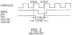
- Primary data signals are produced according to a clock signal transition (Clock A of FIG. 2 ) of a system clock signal.
- the clock signal transition (Clock A) must be such that the receiving component can read, i.e., sample, the primary data signal by the next transition (Clock B) of the system clock signal.
- a normal 'low' going data pulse is provided in response to a first clock transition (Clock A) and remains active during a full clock period, until the occurrence of the next clock transition (Clock B of FIG. 2 ) plus Hold Time.
- a synchronous digital signal capture system is provided.
- the synchronous digital signal capture system 100 includes a first flip-flop 102 and a synchronization module 104.
- the first flip-flop 102 includes a control input (D), a clock input (CK) and a data output (Q1).
- the control input receives a logic control signal and the clock input receives a first clock signal, i.e., a system clock (Clock_1) having a first frequency.
- the data output provides a synchronized data signal (Q1_OUT) based on the logic control signal.
- Q1_OUT is a logic 'low' in response to the logic control signal being a logic 'low'
- Q1_OUT is a logic 'high' in response to the logic control signal being a logic 'high'.
- the first flip-flop 102 further includes an inverting output (QB) to output a synchronous reset signal (QB1_Out) that is a logic inverse of the synchronized data signal (Q1_OUT) generated at the data output to reset the system 100.
- the synchronization module 104 is interposed between an input primary data signal (DATA) and the first flip-flop 102.
- the synchronization module 104 is configured to receive the primary data signal (DATA), the synchronous reset signal (QB1_Out) and the second clock signal (Clock_2).
- the second clock signal (Clock_2) is an accelerated clock signal that has a frequency greater than the frequency of the first clock signal (Clock_1).
- the synchronization module 104 Based on DATA, QB1_Out and Clock_2, the synchronization module 104 generates the logic control signal such that the first flip-flop 102 generates the synchronized signal (Q1_OUT), which may be utilized by various internal logic located downstream from the system 100.
- the primary data signal (DATA) is an active-low pulse having a predetermined pulse-width.
- the synchronization module 104 includes a latching feedback circuit 106 and a control circuit 108.
- the latching feedback circuit 106 includes a second flip-flop 110, and an OR gate 112.
- the second flip-flop 110 has a latch feedback input (D2), an accelerated clock input (CK2), and latch feedback output (Q2).
- the second flip-flop 110 outputs a latch feedback signal (Q2_OUT) at Q2 based on a latching flip-flop control signal (OR1) received at D2 and the accelerated clock signal (Clock_2) input at CK2.
- the accelerated clock signal (Clock_2) is a clock signal having frequency that is greater than Clock_1 input to the first flip-flop 102.
- the accelerated clock signal has frequency that is four times (4X) the frequency of CK input to the first flip-flop.
- the latch feedback signal (Q2_OUT) latches synchronization module 104 as discussed in greater detail below.
- the OR gate 112 includes a first input (X) and a second input (Y).
- the first input X is in electrical communication with QB1 of the first flip-flop 102 to receive the synchronous reset signal (QB1_OUT).
- the second OR input Y is configured to receive a feedback control signal (AND1), which is generated by the control circuit 108 as discussed in greater detail below.
- the control circuit 108 includes a first AND gate 114 to control the latching feedback circuit 106 and a second AND gate 116 to control the first flip-flop 102.
- the first AND gate 114 includes a first data input (A1) to receive the primary data signal (DATA), and a first latch input (B1) in electrical communication with Q2 to receive the delayed feedback signal (Q2_OUT).
- the first AND gate 114 further includes a first control output (AND1) in electrical communication with the second input Y of the OR gate 112. Accordingly, the first AND gate 114 is configured to generate the feedback control signal (AND1) that controls the output of the OR gate 112 (OR1) based on the primary data signal (DATA) and latch feedback signal (Q2_OUT).
- the second AND gate 116 includes a second data input (A2) and a second latch feedback input (B2).
- the second data input (A2) is in electrical communication with A1 to receive the primary data signal (DATA).
- the latch feedback input (B2) is in electrical communication with B1 to receive the latch feedback signal (Q2_OUT).
- the second AND gate 116 further includes a second control output (AND2) in electrical communication with the control input (D1) of the first flip-flop 102 to provide the logic control signal thereto based on the primary data signal (DATA) and the latch feedback signal (Q2_OUT).
- the logic state of the first flip-flop output (Q1) follows the state of the control input (D1) subsequent to each rising transition of the system clock (Clock_1) at CK1.
- first and second AND gates 114, 116 include first and second AND gates 114, 116, it is appreciated by one of ordinary skill in the art that the first and second AND gates 114, 116 may be replaced with a single AND gate having an output connected to D1 of the first flip-flop 102 and the Y input of the OR gate 112, without changing the scope of the present inventive concept.
- At least one embodiment of the 100 may prevent hold time violations in active-low primary data signals, where a single active-low pulse which may be too narrow for to be sampled by the first flip-flop 102 by the next clock transition. That is, the single active-low pulse terminates before being sampled by the next clock transition of the primary clock signal (CK1).
- CK1 primary clock signal
- signals Q1, AND1, AND2, OR1 and Q2 are also 'high'.
- signals AND1, AND2 then OR1 transition 'low'.
- the latch feedback signal (Q2_OUT) output from the second flip-flop 110 transitions 'low' forcing and holding AND1 and AND2 'low', i.e., latching the first and second AND gate 114, 116.
- the first AND gate 114 and the OR gate 112 provide the latch feedback signal to hold the second flip-flop 110 'low' until the first flip-flop 102 is clocked.
- the first flip-flop 102 realizes the control signal from the second AND gate 116 is logic 'low'
- the first flip-flop 102 synchronously outputs Q1_OUT at logic 'low', which may be utilized by downstream internal logic.
- the reset signal (QB1) transitions to logic 'high', thereby forcing the latching flip-flop control signal (OR1) to a logic 'high' which sets the second flip-flop 110 (Q2) 'high' after its next 4X clock-cycle to reset the system 100.
- the first and second AND gate 114, 116 will follow the value of the primary data signal, which will imminently be set to logic 'high'. Accordingly, a logic 'high' at the input of the second AND gate 116 will generate a logic 'high' output from the first flip-flop 102, thereby ending the pulse after one system clock, i.e., the period between CLOCK A and CLOCK B, CLOCK B and CLOCK C, etc.
Landscapes
- Physics & Mathematics (AREA)
- Nonlinear Science (AREA)
- Engineering & Computer Science (AREA)
- Computer Hardware Design (AREA)
- Computing Systems (AREA)
- General Engineering & Computer Science (AREA)
- Mathematical Physics (AREA)
- Synchronisation In Digital Transmission Systems (AREA)
Description
- The present inventive concept relates generally to digital circuit systems, and more specifically, to a synchronous digital system that prevents hold time violations.
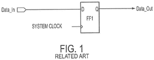
- Conventional digital circuit systems, as illustrated in
FIG. 1 , typically include one or more flip-flops that can be used to store state information. Primary data signals are produced according to a clock signal transition (Clock A ofFIG. 2 ) of a system clock signal. The clock signal transition (Clock A) must be such that the receiving component can read, i.e., sample, the primary data signal by the next transition (Clock B) of the system clock signal. As illustrated in signal diagram resulting from a conventional digital circuit system shown inFIG. 2 , a normal 'low' going data pulse is provided in response to a first clock transition (Clock A) and remains active during a full clock period, until the occurrence of the next clock transition (Clock B ofFIG. 2 ) plus Hold Time. Digital components, however, may provide narrow output pulses that terminate before the completion of a full clock period in width. The premature termination of the pulsed data signal may result in a Hold Time Violation (refer to Data with Hold Time Violation shown inFIG. 2 ). The Hold Time Violation causes receiving components to miss these narrower pulses, which would normally be sampled during the next clock transition, thereby preventing the narrow pulses from being sampled.US 6738442 B1 relates to a pulse detection and synchronization system. - According to one embodiment of the present inventive concept (claim 1), a synchronous digital signal capture system is provided.
- In another embodiment (claim 5), a method is provided.
- Additional features are realized through the techniques of the present inventive concept. Other embodiments of the inventive concept are described in detail herein and are considered a part of the claimed inventive concept. For a better understanding of the inventive concept with the features, refer to the description and to the drawings.
- The subject matter which is regarded as the inventive concept is particularly pointed out and distinctly claimed in the claims at the conclusion of the specification. The forgoing and other features of the inventive concept are apparent from the following detailed description taken in conjunction with the accompanying drawings in which:
-
Figure 1 illustrates a schematic of a conventional digital circuit system; -
Figure 2 is a signal diagram of the conventional digital circuit system illustrated inFigure 1 ; -
Figure 3 is a schematic of a synchronous digital signal capture system according to an embodiment of present inventive concept; and -
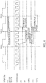
Figure 4 is a signal diagram of the synchronous digital signal capture system illustrated inFigure 3 according to an embodiment of the present inventive concept. - Referring now to
FIG. 3 , a schematic of a synchronous digitalsignal capture system 100 is illustrated according to an embodiment of present inventive concept. The synchronous digitalsignal capture system 100 includes a first flip-flop 102 and asynchronization module 104. The first flip-flop 102 includes a control input (D), a clock input (CK) and a data output (Q1). The control input receives a logic control signal and the clock input receives a first clock signal, i.e., a system clock (Clock_1) having a first frequency. The data output provides a synchronized data signal (Q1_OUT) based on the logic control signal. More specifically, Q1_OUT is a logic 'low' in response to the logic control signal being a logic 'low', and Q1_OUT is a logic 'high' in response to the logic control signal being a logic 'high'. The first flip-flop 102 further includes an inverting output (QB) to output a synchronous reset signal (QB1_Out) that is a logic inverse of the synchronized data signal (Q1_OUT) generated at the data output to reset thesystem 100. - The
synchronization module 104 is interposed between an input primary data signal (DATA) and the first flip-flop 102. Thesynchronization module 104 is configured to receive the primary data signal (DATA), the synchronous reset signal (QB1_Out) and the second clock signal (Clock_2). The second clock signal (Clock_2) is an accelerated clock signal that has a frequency greater than the frequency of the first clock signal (Clock_1). Based on DATA, QB1_Out and Clock_2, thesynchronization module 104 generates the logic control signal such that the first flip-flop 102 generates the synchronized signal (Q1_OUT), which may be utilized by various internal logic located downstream from thesystem 100. In at least one embodiment, the primary data signal (DATA) is an active-low pulse having a predetermined pulse-width. - The
synchronization module 104 includes alatching feedback circuit 106 and acontrol circuit 108. Thelatching feedback circuit 106 includes a second flip-flop 110, and anOR gate 112. The second flip-flop 110 has a latch feedback input (D2), an accelerated clock input (CK2), and latch feedback output (Q2). The second flip-flop 110 outputs a latch feedback signal (Q2_OUT) at Q2 based on a latching flip-flop control signal (OR1) received at D2 and the accelerated clock signal (Clock_2) input at CK2. As mentioned above, the accelerated clock signal (Clock_2) is a clock signal having frequency that is greater than Clock_1 input to the first flip-flop 102. In at least one example according the present inventive concept, the accelerated clock signal has frequency that is four times (4X) the frequency of CK input to the first flip-flop. The latch feedback signal (Q2_OUT)latches synchronization module 104 as discussed in greater detail below. - The
OR gate 112 includes a first input (X) and a second input (Y). The first input X is in electrical communication with QB1 of the first flip-flop 102 to receive the synchronous reset signal (QB1_OUT). The second OR input Y is configured to receive a feedback control signal (AND1), which is generated by thecontrol circuit 108 as discussed in greater detail below. Based on AND1 and the QB1_OUT, theOR gate 112 generates a control signal (OR1) that exists in either a first state (OR1 = 0), which operates as a latch control signal, or a second state (OR1 = 1) which operates as a latch reset signal. The latch control signal commands the second flip-flop 110 to generate the latch feedback control signal (Q2_OUT = 0), while the latch reset control signal resets the second flip-flop 110 (Q2_OUT = 1). - The
control circuit 108 includes a first ANDgate 114 to control thelatching feedback circuit 106 and a second ANDgate 116 to control the first flip-flop 102. The first ANDgate 114 includes a first data input (A1) to receive the primary data signal (DATA), and a first latch input (B1) in electrical communication with Q2 to receive the delayed feedback signal (Q2_OUT). The first ANDgate 114 further includes a first control output (AND1) in electrical communication with the second input Y of theOR gate 112. Accordingly, the first ANDgate 114 is configured to generate the feedback control signal (AND1) that controls the output of the OR gate 112 (OR1) based on the primary data signal (DATA) and latch feedback signal (Q2_OUT). - The second AND
gate 116 includes a second data input (A2) and a second latch feedback input (B2). The second data input (A2) is in electrical communication with A1 to receive the primary data signal (DATA). The latch feedback input (B2) is in electrical communication with B1 to receive the latch feedback signal (Q2_OUT). The second ANDgate 116 further includes a second control output (AND2) in electrical communication with the control input (D1) of the first flip-flop 102 to provide the logic control signal thereto based on the primary data signal (DATA) and the latch feedback signal (Q2_OUT). The logic state of the first flip-flop output (Q1) follows the state of the control input (D1) subsequent to each rising transition of the system clock (Clock_1) at CK1. Although the embodiment illustrated inFIG. 3 includes first and second ANDgates gates flop 102 and the Y input of theOR gate 112, without changing the scope of the present inventive concept. - With reference now to the signal diagram illustrated in
FIG. 4 , operation of the synchronous digitalsignal capture system 100 will be described according to an embodiment of the present inventive concept. More specifically, at least one embodiment of the 100 may prevent hold time violations in active-low primary data signals, where a single active-low pulse which may be too narrow for to be sampled by the first flip-flop 102 by the next clock transition. That is, the single active-low pulse terminates before being sampled by the next clock transition of the primary clock signal (CK1). At normal steady state with DATA at logic 'high', signals Q1, AND1, AND2, OR1 and Q2 are also 'high'. When DATA transitions 'low', signals AND1, AND2 then OR1 transition 'low'. Within a quarter clock cycle, the latch feedback signal (Q2_OUT) output from the second flip-flop 110 transitions 'low' forcing and holding AND1 and AND2 'low', i.e., latching the first and second ANDgate - The first AND
gate 114 and the ORgate 112 provide the latch feedback signal to hold the second flip-flop 110 'low' until the first flip-flop 102 is clocked. When the first flip-flop 102 realizes the control signal from the second ANDgate 116 is logic 'low', the first flip-flop 102 synchronously outputs Q1_OUT at logic 'low', which may be utilized by downstream internal logic. Further, when Q1_OUT is logic 'low', the reset signal (QB1) transitions to logic 'high', thereby forcing the latching flip-flop control signal (OR1) to a logic 'high' which sets the second flip-flop 110 (Q2) 'high' after its next 4X clock-cycle to reset thesystem 100. With Q2 'high', the first and second ANDgate gate 116 will generate a logic 'high' output from the first flip-flop 102, thereby ending the pulse after one system clock, i.e., the period between CLOCK A and CLOCK B, CLOCK B and CLOCK C, etc. - The terminology used herein is for the purpose of describing particular embodiments only and is not intended to be limiting of the inventive concept. As used herein, the singular forms "a", "an" and "the" are intended to include the plural forms as well, unless the context clearly indicates otherwise. It will be further understood that the terms "comprises" and/or "comprising," when used in this specification, specify the presence of stated features, integers, steps, operations, elements, and/or components, but do not preclude the presence or addition of one more other features, integers, steps, operations, element components, and/or groups thereof.
- The corresponding structures, materials, acts, and equivalents of all means or step plus function elements in the claims below are intended to include any structure, material, or act for performing the function in combination with other claimed elements as specifically claimed. The embodiments presented are disclosed in order to best explain the principles of the inventive concept and the practical application, and to enable others of ordinary skill in the art to understand the inventive concept for various embodiments with various modifications as are suited to the particular use contemplated.
- While various embodiments of the inventive concept had been described, it will be understood that those skilled in the art, both now and in the future, may make various modifications to the embodiments which fall within the scope of the claims which follow. These claims should be construed to maintain the proper protection for the invention first described.
Claims (10)
- A synchronous digital signal capture system, comprising:a first flip-flop (102) including a first input (D1) to receive a logic control signal (AND2) and a second input (CK1) to receive a first clock signal (Clock 1) having a first frequency, the first flip-flop configured to output a synchronized data signal (Q1) based on the logic control signal (AND2), and to generate a synchronous reset signal (QB1_OUT) that is a logic inverse of the synchronized data signal;a synchronization module (104) including an input to receive a primary data signal (DATA) and an output in electrical communication with the first flip-flop; the synchronization module being configured to generate the logic control signal based on the primary data signal, the synchronous reset signal and a second clock signal such that the first flip-flop generates the synchronized data signal; wherein the synchronization module comprises: a latching feedback circuit (106) to generate a latch feedback signal (Q2_Out), wherein the latching feedback circuit comprises:an OR gate (112) including a first input (X input) to receive the synchronous reset signal and a second input (Y input) to receive a feedback control signal (AND1), and including an output to output a latching flip-flop control signal (OR1) that is generated based on the feedback control signal (AND1) and the synchronous reset signal (QB!_OUT);a second flip-flop (110) including a first input (D2) to receive the latching flip-flop control signal (OR1) and a second input (CK2) to receive the second clock signal, and including an output (Q2) to output the latch feedback signal (Q2_Out) that is generated based on the latching flip-flop control signal (OR1) and the second clock signal (Clock 2); anda control circuit (108) in electrical communication with the first flip-flop (102) and the latching feedback circuit (106), the control circuit comprising:a first AND gate (114) including a first input (A1) to receive the primary data signal (DATA) and a second input (B1) connected to the output (Q2) of the second flip-flop (110) to receive the latch feedback signal (Q2_Out), and including an output connected to the second Output (Y input) of the OR GATE (112) to deliver the feedback control signal (AND1);a second AND gate (116) including a first input (A2) connected to the first input (A1) of the first AND gate (114) and configured to receive the primary data signal (DATA), and a second input (B2) to receive the latch feedback signal (Q2_Out), and including an output connected to the first input (D1) of the first flip-flop (102), the logic control signal (AND2) in response to receiving, as inputs, the latch feedback signal (Q2_Out) and the primary data signal (DATA).
- The synchronous digital signal capture system of claim 1, wherein the synchronized data signal is a logic low in response to the logic control signal being a logic low and the synchronized data signal is a logic high in response to the logic control signal being a logic high.
- The synchronous digital signal capture system of claim 1, wherein the second clock signal has a frequency that is greater than the frequency of the first clock signal.
- The synchronous digital capture system of claim 1, wherein
the second AND gate configured to output the logic control signal to the first flip-flop (102) such that first flip-flop (102) generates a logic high after one signal pulse of the first clock (CK1) in response to the second AND gate (116) outputting a logic high. - A method of synchronously capturing a digital signal using the synchronous digital signal capture system as defined in any preceding claim, the method comprising:receiving a logic control signal and a first clock signal having a first frequency;outputting a synchronized data signal based on the logic control signal;generating a synchronous reset signal that is a logic inverse of the synchronized data signal; andreceiving a primary data signal;generating the logic control signal based on the primary data signal, the synchronous reset signal and a second clock signal;generating the synchronized data signal in response to generating the logic control signal;generating a latch feedback signal;generating the logic control signal in response to, as inputs, the latch feedback signal and the primary data signal.
- The method of claim 5, wherein synchronized data signal is a logic low in response to the logic control signal being a logic low and the synchronized data signal is a logic high in response to the logic control signal being a logic high.
- The method of claim 6, further comprising generating a latch feedback signal based on a latching control signal and the second clock signal.
- The method of claim 7, further comprising generating the second clock signal having a frequency greater than the frequency of the first clock signal.
- The method of claim 8, further comprising generating a feedback control signal, and generating the latching flip-flop control signal based on the feedback control signal and the synchronous reset signal, wherein the feedback control signal is generated in response to the primary data signal and the latch feedback signal.
- The method of claim 9, further comprising outputting the logic control signal based on the primary data signal and the latch feedback signal.
Applications Claiming Priority (1)
| Application Number | Priority Date | Filing Date | Title |
|---|---|---|---|
| US13/853,424 US8896347B2 (en) | 2013-03-29 | 2013-03-29 | Synchronous input signal capture system |
Publications (2)
| Publication Number | Publication Date |
|---|---|
| EP2784938A1 EP2784938A1 (en) | 2014-10-01 |
| EP2784938B1 true EP2784938B1 (en) | 2021-09-01 |
Family
ID=50693423
Family Applications (1)
| Application Number | Title | Priority Date | Filing Date |
|---|---|---|---|
| EP14161767.0A Active EP2784938B1 (en) | 2013-03-29 | 2014-03-26 | Synchronous input signal capture system |
Country Status (2)
| Country | Link |
|---|---|
| US (1) | US8896347B2 (en) |
| EP (1) | EP2784938B1 (en) |
Families Citing this family (2)
| Publication number | Priority date | Publication date | Assignee | Title |
|---|---|---|---|---|
| CN111010152B (en) * | 2019-12-26 | 2020-08-04 | 荣湃半导体(上海)有限公司 | Signal shaping circuit |
| CN114661498B (en) * | 2020-12-22 | 2025-09-16 | 扬智科技股份有限公司 | electronic devices |
Family Cites Families (9)
| Publication number | Priority date | Publication date | Assignee | Title |
|---|---|---|---|---|
| USH1796H (en) | 1996-05-02 | 1999-07-06 | Sun Microsystems, Inc. | Method and circuit for eliminating hold time violations in synchronous circuits |
| US6275546B1 (en) * | 1998-06-30 | 2001-08-14 | Hewlett-Packard Company | Glitchless clock switch circuit |
| US6738442B1 (en) | 2000-01-19 | 2004-05-18 | Agere Systems Inc. | Pulse detection and synchronization system |
| US6429698B1 (en) * | 2000-05-02 | 2002-08-06 | Xilinx, Inc. | Clock multiplexer circuit with glitchless switching |
| JP2002182777A (en) * | 2000-12-15 | 2002-06-26 | Mitsubishi Electric Corp | Clock switching circuit |
| JP4790060B2 (en) * | 2007-03-20 | 2011-10-12 | 富士通セミコンダクター株式会社 | Clock signal selection circuit |
| US7471120B2 (en) * | 2007-05-15 | 2008-12-30 | Broadcom Corporation | Clock switch for generation of multi-frequency clock signal |
| JP5193846B2 (en) | 2008-12-25 | 2013-05-08 | 株式会社東芝 | Synchronization circuit |
| TWI453569B (en) | 2011-03-18 | 2014-09-21 | Realtek Semiconductor Corp | Signal synchronizing apparatus |
-
2013
- 2013-03-29 US US13/853,424 patent/US8896347B2/en active Active
-
2014
- 2014-03-26 EP EP14161767.0A patent/EP2784938B1/en active Active
Also Published As
| Publication number | Publication date |
|---|---|
| US20140292370A1 (en) | 2014-10-02 |
| US8896347B2 (en) | 2014-11-25 |
| EP2784938A1 (en) | 2014-10-01 |
Similar Documents
| Publication | Publication Date | Title |
|---|---|---|
| US8686773B1 (en) | In-system margin measurement circuit | |
| US9325487B1 (en) | Systems and methods for transferring a signal from a first clock domain to a second clock domain | |
| EP2104267B1 (en) | Clock domain crossing synchronizer with feedback | |
| CN101135921B (en) | Multi-clock switching device and switching method thereof | |
| KR101966084B1 (en) | Signal value storage circuitry with transition detector | |
| CN110247656B (en) | Damaged clock detection circuit for phase-locked loop | |
| US9106235B2 (en) | Mesochronous synchronizer with delay-line phase detector | |
| KR101982194B1 (en) | Delay control circuit and clock generating circuit including the same | |
| US11451236B2 (en) | Metastabile state detection device and method, and ADC circuit | |
| US9899992B1 (en) | Low power adaptive synchronizer | |
| US7936855B2 (en) | Oversampling data recovery circuit and method for a receiver | |
| US8896347B2 (en) | Synchronous input signal capture system | |
| US6373312B1 (en) | Precision, high speed delay system for providing delayed clock edges with new delay values every clock period | |
| US7042267B1 (en) | Gated clock circuit with a substantially increased control signal delay | |
| US6531905B1 (en) | Flip-flop with metastability reduction | |
| EP2928082B1 (en) | Clock enabling circuit | |
| JP2002176341A (en) | Clock control circuit | |
| US8400188B2 (en) | Methods, systems and arrangements for edge detection | |
| US20070183549A1 (en) | Adaptive variable length pulse synchronizer | |
| US6041418A (en) | Race free and technology independent flag generating circuitry associated with two asynchronous clocks | |
| EP4202602A1 (en) | Integrated circuit reset method and integrated circuit | |
| EP1618660B1 (en) | Enabling method to prevent glitches in waveform | |
| JPS63200071A (en) | Trigger signal generator and trigger signal generating method | |
| JP2010021950A (en) | Asynchronous interface circuit and method | |
| EP0624296A1 (en) | Means to avoid data distorsion in clock-synchronized signal sampling |
Legal Events
| Date | Code | Title | Description |
|---|---|---|---|
| 17P | Request for examination filed |
Effective date: 20140326 |
|
| AK | Designated contracting states |
Kind code of ref document: A1 Designated state(s): AL AT BE BG CH CY CZ DE DK EE ES FI FR GB GR HR HU IE IS IT LI LT LU LV MC MK MT NL NO PL PT RO RS SE SI SK SM TR |
|
| AX | Request for extension of the european patent |
Extension state: BA ME |
|
| PUAI | Public reference made under article 153(3) epc to a published international application that has entered the european phase |
Free format text: ORIGINAL CODE: 0009012 |
|
| R17P | Request for examination filed (corrected) |
Effective date: 20150401 |
|
| RBV | Designated contracting states (corrected) |
Designated state(s): AL AT BE BG CH CY CZ DE DK EE ES FI FR GB GR HR HU IE IS IT LI LT LU LV MC MK MT NL NO PL PT RO RS SE SI SK SM TR |
|
| STAA | Information on the status of an ep patent application or granted ep patent |
Free format text: STATUS: EXAMINATION IS IN PROGRESS |
|
| 17Q | First examination report despatched |
Effective date: 20180716 |
|
| GRAP | Despatch of communication of intention to grant a patent |
Free format text: ORIGINAL CODE: EPIDOSNIGR1 |
|
| STAA | Information on the status of an ep patent application or granted ep patent |
Free format text: STATUS: GRANT OF PATENT IS INTENDED |
|
| INTG | Intention to grant announced |
Effective date: 20210412 |
|
| RAP3 | Party data changed (applicant data changed or rights of an application transferred) |
Owner name: HAMILTON SUNDSTRAND CORPORATION |
|
| GRAS | Grant fee paid |
Free format text: ORIGINAL CODE: EPIDOSNIGR3 |
|
| GRAA | (expected) grant |
Free format text: ORIGINAL CODE: 0009210 |
|
| STAA | Information on the status of an ep patent application or granted ep patent |
Free format text: STATUS: THE PATENT HAS BEEN GRANTED |
|
| AK | Designated contracting states |
Kind code of ref document: B1 Designated state(s): AL AT BE BG CH CY CZ DE DK EE ES FI FR GB GR HR HU IE IS IT LI LT LU LV MC MK MT NL NO PL PT RO RS SE SI SK SM TR |
|
| REG | Reference to a national code |
Ref country code: GB Ref legal event code: FG4D |
|
| REG | Reference to a national code |
Ref country code: CH Ref legal event code: EP Ref country code: AT Ref legal event code: REF Ref document number: 1427299 Country of ref document: AT Kind code of ref document: T Effective date: 20210915 |
|
| REG | Reference to a national code |
Ref country code: DE Ref legal event code: R096 Ref document number: 602014079800 Country of ref document: DE |
|
| REG | Reference to a national code |
Ref country code: IE Ref legal event code: FG4D |
|
| REG | Reference to a national code |
Ref country code: LT Ref legal event code: MG9D |
|
| REG | Reference to a national code |
Ref country code: NL Ref legal event code: MP Effective date: 20210901 |
|
| PG25 | Lapsed in a contracting state [announced via postgrant information from national office to epo] |
Ref country code: BG Free format text: LAPSE BECAUSE OF FAILURE TO SUBMIT A TRANSLATION OF THE DESCRIPTION OR TO PAY THE FEE WITHIN THE PRESCRIBED TIME-LIMIT Effective date: 20211201 Ref country code: LT Free format text: LAPSE BECAUSE OF FAILURE TO SUBMIT A TRANSLATION OF THE DESCRIPTION OR TO PAY THE FEE WITHIN THE PRESCRIBED TIME-LIMIT Effective date: 20210901 Ref country code: ES Free format text: LAPSE BECAUSE OF FAILURE TO SUBMIT A TRANSLATION OF THE DESCRIPTION OR TO PAY THE FEE WITHIN THE PRESCRIBED TIME-LIMIT Effective date: 20210901 Ref country code: FI Free format text: LAPSE BECAUSE OF FAILURE TO SUBMIT A TRANSLATION OF THE DESCRIPTION OR TO PAY THE FEE WITHIN THE PRESCRIBED TIME-LIMIT Effective date: 20210901 Ref country code: NO Free format text: LAPSE BECAUSE OF FAILURE TO SUBMIT A TRANSLATION OF THE DESCRIPTION OR TO PAY THE FEE WITHIN THE PRESCRIBED TIME-LIMIT Effective date: 20211201 Ref country code: SE Free format text: LAPSE BECAUSE OF FAILURE TO SUBMIT A TRANSLATION OF THE DESCRIPTION OR TO PAY THE FEE WITHIN THE PRESCRIBED TIME-LIMIT Effective date: 20210901 Ref country code: RS Free format text: LAPSE BECAUSE OF FAILURE TO SUBMIT A TRANSLATION OF THE DESCRIPTION OR TO PAY THE FEE WITHIN THE PRESCRIBED TIME-LIMIT Effective date: 20210901 Ref country code: HR Free format text: LAPSE BECAUSE OF FAILURE TO SUBMIT A TRANSLATION OF THE DESCRIPTION OR TO PAY THE FEE WITHIN THE PRESCRIBED TIME-LIMIT Effective date: 20210901 |
|
| REG | Reference to a national code |
Ref country code: AT Ref legal event code: MK05 Ref document number: 1427299 Country of ref document: AT Kind code of ref document: T Effective date: 20210901 |
|
| PG25 | Lapsed in a contracting state [announced via postgrant information from national office to epo] |
Ref country code: PL Free format text: LAPSE BECAUSE OF FAILURE TO SUBMIT A TRANSLATION OF THE DESCRIPTION OR TO PAY THE FEE WITHIN THE PRESCRIBED TIME-LIMIT Effective date: 20210901 Ref country code: LV Free format text: LAPSE BECAUSE OF FAILURE TO SUBMIT A TRANSLATION OF THE DESCRIPTION OR TO PAY THE FEE WITHIN THE PRESCRIBED TIME-LIMIT Effective date: 20210901 Ref country code: GR Free format text: LAPSE BECAUSE OF FAILURE TO SUBMIT A TRANSLATION OF THE DESCRIPTION OR TO PAY THE FEE WITHIN THE PRESCRIBED TIME-LIMIT Effective date: 20211202 |
|
| PG25 | Lapsed in a contracting state [announced via postgrant information from national office to epo] |
Ref country code: AT Free format text: LAPSE BECAUSE OF FAILURE TO SUBMIT A TRANSLATION OF THE DESCRIPTION OR TO PAY THE FEE WITHIN THE PRESCRIBED TIME-LIMIT Effective date: 20210901 |
|
| PG25 | Lapsed in a contracting state [announced via postgrant information from national office to epo] |
Ref country code: IS Free format text: LAPSE BECAUSE OF FAILURE TO SUBMIT A TRANSLATION OF THE DESCRIPTION OR TO PAY THE FEE WITHIN THE PRESCRIBED TIME-LIMIT Effective date: 20220101 Ref country code: SM Free format text: LAPSE BECAUSE OF FAILURE TO SUBMIT A TRANSLATION OF THE DESCRIPTION OR TO PAY THE FEE WITHIN THE PRESCRIBED TIME-LIMIT Effective date: 20210901 Ref country code: SK Free format text: LAPSE BECAUSE OF FAILURE TO SUBMIT A TRANSLATION OF THE DESCRIPTION OR TO PAY THE FEE WITHIN THE PRESCRIBED TIME-LIMIT Effective date: 20210901 Ref country code: RO Free format text: LAPSE BECAUSE OF FAILURE TO SUBMIT A TRANSLATION OF THE DESCRIPTION OR TO PAY THE FEE WITHIN THE PRESCRIBED TIME-LIMIT Effective date: 20210901 Ref country code: PT Free format text: LAPSE BECAUSE OF FAILURE TO SUBMIT A TRANSLATION OF THE DESCRIPTION OR TO PAY THE FEE WITHIN THE PRESCRIBED TIME-LIMIT Effective date: 20220103 Ref country code: NL Free format text: LAPSE BECAUSE OF FAILURE TO SUBMIT A TRANSLATION OF THE DESCRIPTION OR TO PAY THE FEE WITHIN THE PRESCRIBED TIME-LIMIT Effective date: 20210901 Ref country code: EE Free format text: LAPSE BECAUSE OF FAILURE TO SUBMIT A TRANSLATION OF THE DESCRIPTION OR TO PAY THE FEE WITHIN THE PRESCRIBED TIME-LIMIT Effective date: 20210901 Ref country code: CZ Free format text: LAPSE BECAUSE OF FAILURE TO SUBMIT A TRANSLATION OF THE DESCRIPTION OR TO PAY THE FEE WITHIN THE PRESCRIBED TIME-LIMIT Effective date: 20210901 Ref country code: AL Free format text: LAPSE BECAUSE OF FAILURE TO SUBMIT A TRANSLATION OF THE DESCRIPTION OR TO PAY THE FEE WITHIN THE PRESCRIBED TIME-LIMIT Effective date: 20210901 |
|
| REG | Reference to a national code |
Ref country code: DE Ref legal event code: R097 Ref document number: 602014079800 Country of ref document: DE |
|
| PLBE | No opposition filed within time limit |
Free format text: ORIGINAL CODE: 0009261 |
|
| STAA | Information on the status of an ep patent application or granted ep patent |
Free format text: STATUS: NO OPPOSITION FILED WITHIN TIME LIMIT |
|
| PG25 | Lapsed in a contracting state [announced via postgrant information from national office to epo] |
Ref country code: IT Free format text: LAPSE BECAUSE OF FAILURE TO SUBMIT A TRANSLATION OF THE DESCRIPTION OR TO PAY THE FEE WITHIN THE PRESCRIBED TIME-LIMIT Effective date: 20210901 Ref country code: DK Free format text: LAPSE BECAUSE OF FAILURE TO SUBMIT A TRANSLATION OF THE DESCRIPTION OR TO PAY THE FEE WITHIN THE PRESCRIBED TIME-LIMIT Effective date: 20210901 |
|
| 26N | No opposition filed |
Effective date: 20220602 |
|
| PG25 | Lapsed in a contracting state [announced via postgrant information from national office to epo] |
Ref country code: SI Free format text: LAPSE BECAUSE OF FAILURE TO SUBMIT A TRANSLATION OF THE DESCRIPTION OR TO PAY THE FEE WITHIN THE PRESCRIBED TIME-LIMIT Effective date: 20210901 |
|
| PG25 | Lapsed in a contracting state [announced via postgrant information from national office to epo] |
Ref country code: MC Free format text: LAPSE BECAUSE OF FAILURE TO SUBMIT A TRANSLATION OF THE DESCRIPTION OR TO PAY THE FEE WITHIN THE PRESCRIBED TIME-LIMIT Effective date: 20210901 |
|
| REG | Reference to a national code |
Ref country code: CH Ref legal event code: PL |
|
| REG | Reference to a national code |
Ref country code: BE Ref legal event code: MM Effective date: 20220331 |
|
| PG25 | Lapsed in a contracting state [announced via postgrant information from national office to epo] |
Ref country code: LU Free format text: LAPSE BECAUSE OF NON-PAYMENT OF DUE FEES Effective date: 20220326 Ref country code: LI Free format text: LAPSE BECAUSE OF NON-PAYMENT OF DUE FEES Effective date: 20220331 Ref country code: IE Free format text: LAPSE BECAUSE OF NON-PAYMENT OF DUE FEES Effective date: 20220326 Ref country code: CH Free format text: LAPSE BECAUSE OF NON-PAYMENT OF DUE FEES Effective date: 20220331 |
|
| PG25 | Lapsed in a contracting state [announced via postgrant information from national office to epo] |
Ref country code: BE Free format text: LAPSE BECAUSE OF NON-PAYMENT OF DUE FEES Effective date: 20220331 |
|
| P01 | Opt-out of the competence of the unified patent court (upc) registered |
Effective date: 20230522 |
|
| PG25 | Lapsed in a contracting state [announced via postgrant information from national office to epo] |
Ref country code: HU Free format text: LAPSE BECAUSE OF FAILURE TO SUBMIT A TRANSLATION OF THE DESCRIPTION OR TO PAY THE FEE WITHIN THE PRESCRIBED TIME-LIMIT; INVALID AB INITIO Effective date: 20140326 |
|
| PG25 | Lapsed in a contracting state [announced via postgrant information from national office to epo] |
Ref country code: MK Free format text: LAPSE BECAUSE OF FAILURE TO SUBMIT A TRANSLATION OF THE DESCRIPTION OR TO PAY THE FEE WITHIN THE PRESCRIBED TIME-LIMIT Effective date: 20210901 Ref country code: CY Free format text: LAPSE BECAUSE OF FAILURE TO SUBMIT A TRANSLATION OF THE DESCRIPTION OR TO PAY THE FEE WITHIN THE PRESCRIBED TIME-LIMIT Effective date: 20210901 |
|
| PG25 | Lapsed in a contracting state [announced via postgrant information from national office to epo] |
Ref country code: MT Free format text: LAPSE BECAUSE OF FAILURE TO SUBMIT A TRANSLATION OF THE DESCRIPTION OR TO PAY THE FEE WITHIN THE PRESCRIBED TIME-LIMIT Effective date: 20210901 |
|
| PGFP | Annual fee paid to national office [announced via postgrant information from national office to epo] |
Ref country code: DE Payment date: 20250218 Year of fee payment: 12 |
|
| PGFP | Annual fee paid to national office [announced via postgrant information from national office to epo] |
Ref country code: FR Payment date: 20250219 Year of fee payment: 12 |
|
| PGFP | Annual fee paid to national office [announced via postgrant information from national office to epo] |
Ref country code: GB Payment date: 20250221 Year of fee payment: 12 |
|
| PG25 | Lapsed in a contracting state [announced via postgrant information from national office to epo] |
Ref country code: TR Free format text: LAPSE BECAUSE OF FAILURE TO SUBMIT A TRANSLATION OF THE DESCRIPTION OR TO PAY THE FEE WITHIN THE PRESCRIBED TIME-LIMIT Effective date: 20210901 |