EP2784829A1 - Cis/cigs solar cell having a rear tco layer and production method therefor - Google Patents
Cis/cigs solar cell having a rear tco layer and production method therefor Download PDFInfo
- Publication number
- EP2784829A1 EP2784829A1 EP12852335.4A EP12852335A EP2784829A1 EP 2784829 A1 EP2784829 A1 EP 2784829A1 EP 12852335 A EP12852335 A EP 12852335A EP 2784829 A1 EP2784829 A1 EP 2784829A1
- Authority
- EP
- European Patent Office
- Prior art keywords
- layer
- light
- substrate
- solar cell
- cis
- Prior art date
- Legal status (The legal status is an assumption and is not a legal conclusion. Google has not performed a legal analysis and makes no representation as to the accuracy of the status listed.)
- Granted
Links
Images

Classifications
-
- H—ELECTRICITY
- H10—SEMICONDUCTOR DEVICES; ELECTRIC SOLID-STATE DEVICES NOT OTHERWISE PROVIDED FOR
- H10F—INORGANIC SEMICONDUCTOR DEVICES SENSITIVE TO INFRARED RADIATION, LIGHT, ELECTROMAGNETIC RADIATION OF SHORTER WAVELENGTH OR CORPUSCULAR RADIATION
- H10F10/00—Individual photovoltaic cells, e.g. solar cells
- H10F10/10—Individual photovoltaic cells, e.g. solar cells having potential barriers
- H10F10/16—Photovoltaic cells having only PN heterojunction potential barriers
- H10F10/167—Photovoltaic cells having only PN heterojunction potential barriers comprising Group I-III-VI materials, e.g. CdS/CuInSe2 [CIS] heterojunction photovoltaic cells
-
- H—ELECTRICITY
- H10—SEMICONDUCTOR DEVICES; ELECTRIC SOLID-STATE DEVICES NOT OTHERWISE PROVIDED FOR
- H10F—INORGANIC SEMICONDUCTOR DEVICES SENSITIVE TO INFRARED RADIATION, LIGHT, ELECTROMAGNETIC RADIATION OF SHORTER WAVELENGTH OR CORPUSCULAR RADIATION
- H10F19/00—Integrated devices, or assemblies of multiple devices, comprising at least one photovoltaic cell covered by group H10F10/00, e.g. photovoltaic modules
-
- H—ELECTRICITY
- H10—SEMICONDUCTOR DEVICES; ELECTRIC SOLID-STATE DEVICES NOT OTHERWISE PROVIDED FOR
- H10F—INORGANIC SEMICONDUCTOR DEVICES SENSITIVE TO INFRARED RADIATION, LIGHT, ELECTROMAGNETIC RADIATION OF SHORTER WAVELENGTH OR CORPUSCULAR RADIATION
- H10F71/00—Manufacture or treatment of devices covered by this subclass
-
- H—ELECTRICITY
- H10—SEMICONDUCTOR DEVICES; ELECTRIC SOLID-STATE DEVICES NOT OTHERWISE PROVIDED FOR
- H10F—INORGANIC SEMICONDUCTOR DEVICES SENSITIVE TO INFRARED RADIATION, LIGHT, ELECTROMAGNETIC RADIATION OF SHORTER WAVELENGTH OR CORPUSCULAR RADIATION
- H10F77/00—Constructional details of devices covered by this subclass
-
- H—ELECTRICITY
- H10—SEMICONDUCTOR DEVICES; ELECTRIC SOLID-STATE DEVICES NOT OTHERWISE PROVIDED FOR
- H10F—INORGANIC SEMICONDUCTOR DEVICES SENSITIVE TO INFRARED RADIATION, LIGHT, ELECTROMAGNETIC RADIATION OF SHORTER WAVELENGTH OR CORPUSCULAR RADIATION
- H10F77/00—Constructional details of devices covered by this subclass
- H10F77/10—Semiconductor bodies
- H10F77/12—Active materials
- H10F77/126—Active materials comprising only Group I-III-VI chalcopyrite materials, e.g. CuInSe2, CuGaSe2 or CuInGaSe2 [CIGS]
-
- H—ELECTRICITY
- H10—SEMICONDUCTOR DEVICES; ELECTRIC SOLID-STATE DEVICES NOT OTHERWISE PROVIDED FOR
- H10F—INORGANIC SEMICONDUCTOR DEVICES SENSITIVE TO INFRARED RADIATION, LIGHT, ELECTROMAGNETIC RADIATION OF SHORTER WAVELENGTH OR CORPUSCULAR RADIATION
- H10F77/00—Constructional details of devices covered by this subclass
- H10F77/20—Electrodes
- H10F77/206—Electrodes for devices having potential barriers
- H10F77/211—Electrodes for devices having potential barriers for photovoltaic cells
- H10F77/219—Arrangements for electrodes of back-contact photovoltaic cells
-
- H—ELECTRICITY
- H10—SEMICONDUCTOR DEVICES; ELECTRIC SOLID-STATE DEVICES NOT OTHERWISE PROVIDED FOR
- H10F—INORGANIC SEMICONDUCTOR DEVICES SENSITIVE TO INFRARED RADIATION, LIGHT, ELECTROMAGNETIC RADIATION OF SHORTER WAVELENGTH OR CORPUSCULAR RADIATION
- H10F77/00—Constructional details of devices covered by this subclass
- H10F77/20—Electrodes
- H10F77/244—Electrodes made of transparent conductive layers, e.g. transparent conductive oxide [TCO] layers
-
- H—ELECTRICITY
- H10—SEMICONDUCTOR DEVICES; ELECTRIC SOLID-STATE DEVICES NOT OTHERWISE PROVIDED FOR
- H10F—INORGANIC SEMICONDUCTOR DEVICES SENSITIVE TO INFRARED RADIATION, LIGHT, ELECTROMAGNETIC RADIATION OF SHORTER WAVELENGTH OR CORPUSCULAR RADIATION
- H10F77/00—Constructional details of devices covered by this subclass
- H10F77/30—Coatings
- H10F77/306—Coatings for devices having potential barriers
- H10F77/311—Coatings for devices having potential barriers for photovoltaic cells
- H10F77/315—Coatings for devices having potential barriers for photovoltaic cells the coatings being antireflective or having enhancing optical properties
-
- Y—GENERAL TAGGING OF NEW TECHNOLOGICAL DEVELOPMENTS; GENERAL TAGGING OF CROSS-SECTIONAL TECHNOLOGIES SPANNING OVER SEVERAL SECTIONS OF THE IPC; TECHNICAL SUBJECTS COVERED BY FORMER USPC CROSS-REFERENCE ART COLLECTIONS [XRACs] AND DIGESTS
- Y02—TECHNOLOGIES OR APPLICATIONS FOR MITIGATION OR ADAPTATION AGAINST CLIMATE CHANGE
- Y02E—REDUCTION OF GREENHOUSE GAS [GHG] EMISSIONS, RELATED TO ENERGY GENERATION, TRANSMISSION OR DISTRIBUTION
- Y02E10/00—Energy generation through renewable energy sources
- Y02E10/50—Photovoltaic [PV] energy
- Y02E10/541—CuInSe2 material PV cells
-
- Y—GENERAL TAGGING OF NEW TECHNOLOGICAL DEVELOPMENTS; GENERAL TAGGING OF CROSS-SECTIONAL TECHNOLOGIES SPANNING OVER SEVERAL SECTIONS OF THE IPC; TECHNICAL SUBJECTS COVERED BY FORMER USPC CROSS-REFERENCE ART COLLECTIONS [XRACs] AND DIGESTS
- Y02—TECHNOLOGIES OR APPLICATIONS FOR MITIGATION OR ADAPTATION AGAINST CLIMATE CHANGE
- Y02P—CLIMATE CHANGE MITIGATION TECHNOLOGIES IN THE PRODUCTION OR PROCESSING OF GOODS
- Y02P70/00—Climate change mitigation technologies in the production process for final industrial or consumer products
- Y02P70/50—Manufacturing or production processes characterised by the final manufactured product
Definitions
- the present invention relates to a solar cell, and, more particularly, to a CIS/CIGS-based solar cell including a rear TCO layer at the rear side thereof, which can increase a power generation efficiency by disposing a TCO layer and a buffer layer at the rear side thereof to increase the efficiency of a light-absorbing layer, and to a method of manufacturing the same.
- next-generation clean energy sources a solar cell, which is a device for directly converting solar energy into electrical energy, is an energy source that is expected to solve future energy problems because it rarely causes environmental pollution, its energy resource is unrestricted, and its life span is semipermanent.
- Solar cells are classified into various types according to the kind of materials used for a light-absorbing layer.
- a silicon solar cell is generally used.
- the raw material consumption of the thin film-type solar cell is low because it is thin.
- the thin film-type solar cell can be widely used because it is light.
- Research into amorphous silicon, Cd-Te, CIS and CIGS, as raw materials of such a thin film-type solar cell, is actively being conducted.
- a CIS thin film or a CIGS thin film is one of I-III-VI compound semiconductors.
- a CIS thin film solar cell or a CIGS thin film solar cell exhibits the highest conversion efficiency.
- a CIS thin film solar cell or a CIGS thin film solar cell can be manufactured to a thickness of 10 ⁇ m or less and is stable even when it is used for a long period of time, it is considered as a high-efficiency solar cell that can be used in place of a silicon solar cell.
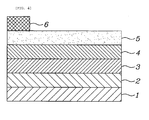
- FIG. 3 shows the structure of a conventional CIS/CIGS-based solar cell employing the CIS or CIGS as a light-absorbing layer.
- the conventional CIS/CIGS-based solar cell including a substrate 1, a molybdenum (Mo) electrode 2, a light-absorbing layer 3, a buffer layer 4, a transparent conducting oxide (TCO) layer 5 and a metal electrode 6, which are sequentially layered from the bottom thereof.
- Mo molybdenum
- TCO transparent conducting oxide
- the conventional CIS/CIGS-based solar cell is problematic in that the amount of light incident upon the light-absorbing layer 3 can be reduced due to the light absorption of the buffer layer 4 disposed on the light-absorbing layer 4. Further, the conventional CIS/CIGS-based solar cell is problematic in that its energy conversion efficiency is decreased because the metal electrode 6 is disposed on the TCO layer 5 in the form of a grid to reduce the amount of incident light with respect to the area thereof.
- an object of the present invention is to provide a solar cell, in which a buffer layer and a TCO layer are disposed at the rear side of a light-absorbing layer, so the amount of light incident on the light-absorbing layer is increased, thereby increasing the energy conversion efficiency of the solar cell.
- an aspect of the present invention provides a CIS/CIGS-based solar cell, including: a substrate; first and second molybdenum electrodes disposed on the substrate at a predetermined interval in parallel with each other; a TCO layer disposed on upper and lateral sides of the second molybdenum electrode; a buffer layer disposed on upper and lateral sides of the TCO layer to compensate for a difference in bandgap between the TCO layer and a light-absorbing layer; the light-absorbing layer disposed on the first molybdenum electrode, the buffer layer and an area of the substrate partially opened between the first molybdenum electrode and the buffer layer; and an antireflection layer disposed on the light-absorbing layer to minimize the reflection of externally-applied light.
- the substrate may be made of any one selected from among glass, stainless steel and polyimide.
- the TCO layer may include an N-type lower transparent conducting film and an I-type upper transparent conducting film.
- the TCO layer may be made of zinc oxide or ITO.
- the buffer layer may be made of any one selected from among cadmium sulfide, zinc sulfide and indium sulfide.
- the light-absorbing layer may be made of any one CIS/CIGS-based compound selected from the group consisting of Cu-In-Se, Cu-In-S, Cu-Ga-S, Cu-Ga-Se, Cu-In-Ga-Se, Cu-In-Ga-Se-(S,Se), Cu-In-Al-Ga-(S,Se) and Cu-In-Al-Ga-Se-S, or may be made of any one CZTS-based compound selected from the group consisting of Cu-Zn-Sn-(Se,S) and Cu-In-Ga-Zn-Sn-(Se,S).
- the antireflection layer may include a lower alumina layer in contact with the light-absorbing layer and an upper magnesium fluoride layer exposed to air.
- Another aspect of the present invention provides a method of manufacturing a CIS/CIGS-based solar cell, including the steps of: a) providing a substrate; b) depositing a molybdenum layer on the substrate and then patterning the molybdenum layer to form first and second molybdenum electrodes disposed on the substrate at a predetermined interval in parallel with each other; c) depositing a TCO layer on the substrate having passed through the step b) and then patterning the TCO layer to form a TCO layer disposed on upper and lateral sides of the second molybdenum electrode; d) depositing a buffer layer on the substrate having passed through the step c) and then patterning the buffer layer to form a buffer layer disposed on upper and lateral sides of the TCO layer; e) forming a light-absorbing layer on the substrate having passed through the step d); and f) forming an antireflection layer on the light-absorbing layer.
- the substrate may be made of any one selected from among glass, stainless steel and polyimide.
- the substrate may be provided by sequentially washing it with acetone, methanol and distilled water and then ultrasonically treating it.
- the deposition of the molybdenum layer may be preformed by sputtering.
- the deposition of the molybdenum layer using sputtering may be performed for 1 ⁇ 30 minutes under the conditions of a power of 0.5 ⁇ 50 kW, a sputtering pressure of 0.1 ⁇ 50 m Torr and an argon (Ar) gas supply of 1 ⁇ 100 sccm.
- the patterning of the molybdenum layer may be preformed by laser scribing.
- the patterning of the molybdenum layer using laser scribing may be performed under the conditions of a laser wavelength of 300 ⁇ 1100 nm and a laser power of 0.3 ⁇ 3 W.
- the TCO layer is made of zinc oxide or ITO.
- the deposition of the TCO layer may be preformed by sputtering.
- the patterning of the TCO layer may be preformed by laser scribing.
- the patterning of the TCO layer using laser scribing may be performed under the conditions of a laser wavelength of 300 ⁇ 1100 nm and a laser power of 0.3 ⁇ 3 W.
- the TCO layer is formed such a way that an N-type transparent conducting film may be deposited and patterned, and then an I-type transparent conducting film may be deposited and patterned to form a double TCO layer.
- the N-type transparent conducting film and the I-type transparent conducting film may be deposited by sputtering, the deposition of the N-type transparent conducting film using sputtering may be performed for 10 ⁇ 100 minutes under the conditions of a power of 50 ⁇ 500 W, a sputtering pressure of 1 ⁇ 50 m Torr, an argon gas supply of 10 ⁇ 100 sccm and an oxygen gas supply of 0.5 ⁇ 10 sccm, and the deposition of the I-type transparent conducting film using sputtering may be performed for 10 ⁇ 100 minutes under the conditions of a power of 50 ⁇ 500 W, a sputtering pressure of 1 ⁇ 50 m Torr and an argon gas supply of 10 ⁇ 100 sccm.
- the buffer layer may be made of any one selected from cadmium sulfide, zinc sulfide and indium sulfide.
- the buffer layer may be formed by immersing the substrate having passed through the step c) into a mixed solution including thiourea, cadmium sulfide and ammonia.
- the buffer layer may be formed by immersing the substrate into the mixed solution at a temperature of 60 ⁇ 100°C for 10 ⁇ 100 minutes.
- the patterning of the buffer layer may be preformed by laser scribing.
- the patterning of the buffer layer using laser scribing may be performed under the conditions of a laser wavelength of 300 ⁇ 600 nm and a laser power of 0.3 ⁇ 3 W.
- the formation of the light-absorbing layer may be preformed by non-vacuum coating or vacuum coating.
- the non-vacuum coating may be any one selected from among spraying, ultrasonic spraying, spin coating, a doctor blade method, screen printing and ink-jet printing.
- the vacuum coating is any one selected from among simultaneous vacuum evaporation, sputtering/selenization and three-stage simultaneous vacuum evaporation.
- the antireflection layer may be formed by sequentially forming a lower alumina layer and an upper magnesium fluoride layer.
- the formation of the alumina layer may be performed by atomic layer deposition (ALD) using gas produced by the reaction of trimethyl aluminum and ozone.
- ALD atomic layer deposition
- the formation of the magnesium fluoride layer may be performed by thermal evaporation using magnesium fluoride pellets.
- Still another aspect of the present invention provides a solar cell module comprising a CIS/CIGS solar cell, the CIS/CIGS solar cell includng: a substrate; first and second molybdenum electrodes disposed on the substrate at a predetermined interval in parallel with each other; a TCO layer disposed on upper and lateral sides of the second molybdenum electrode; a buffer layer disposed on upper and lateral sides of the TCO layer to compensate for a difference in bandgap between the TCO layer and a light-absorbing layer; the light-absorbing layer disposed on the first molybdenum electrode, the buffer layer and an area of the substrate partially opened between the first molybdenum electrode and the buffer layer; and an antireflection layer disposed on the light-absorbing layer to minimize the reflection of externally-applied light.
- a buffer layer and a TCO layer are disposed at the rear side of a light-absorbing layer to prevent the amount of light incident upon the light-absorbing layer from being reduced by removing the incident light obstruction structure disposed on the light-absorbing layer, so the amount of light incident upon the light-absorbing layer can be maximized, thereby increasing the energy conversion efficiency of the solar cell.
- a CIS/CIGS-based solar cell including a TCO layer at the rear side thereof will be described, and then a method of manufacturing the same will be described.
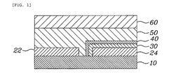
- the CIS/CIGS-based solar cell includes a substrate 10, first and second molybdenum electrodes 22 and 24, a TCO layer 30, a buffer layer 40, a light-absorbing layer 50 and an antireflection layer 60, which are sequentially layered from the bottom thereof.
- the TCO layer 30 and the buffer layer 40 are sequentially disposed on the upper and lateral sides of the second molybdenum electrode 24 to be disposed on the substrate 10 in parallel with each other and spaced apart from the first molybdenum electrode 22.
- the structure of the CIS/CIGS-based solar cell will be described in detail.
- the substrate 10 is a plated structure on which components of a solar cell are disposed and which serves to support the components thereof.
- the substrate is made of glass, but, if necessary, may be made of stainless steel, polyimide or the like.
- the first molybdenum electrode 22 and the second molybdenum electrode 24 are disposed on the substrate 10 in parallel with each other at a predetermined interval.
- the first molybdenum electrode 22 corresponds to a rear electrode of a general thin film solar cell
- the second molybdenum electrode 24 corresponds to a front metal electrode thereof.
- the TCO layer 30 is a transparent conducting layer, and is disposed on the upper and lateral sides of the second molybdenum electrode 24 to cover the second molybdenum electrode 24. Therefore, the first molybdenum electrode 22 and the TCO layer 30 are disposed on the substrate 10 in parallel with each other with the light-absorbing layer 50 being disposed therebetween.
- the TCO layer 30 consists of a lower layer and an upper layer.
- the lower layer is an N-type transparent conducting film
- the upper layer is an I-type transparent conducting film.
- the lower and upper layers can constitute a PIN junction together with the light-absorbing layer 50.
- the TCO layer 30 may be made of a transparent material having electrical conductivity, such as zinc oxide (ZnO), indium tin oxide (ITO) or the like.
- the buffer layer 40 functions to reduce the increase in bandgap between the TCO layer 30 and the light-absorbing layer 50.
- the buffer layer 40 is disposed on the upper and lateral sides of the TCO layer 30 to cover the TCO layer 30. It is preferred that the buffer layer 40 be made of cadmium sulfide (CdS).
- the buffer layer 40 may also be made of an alternative material such as zinc sulfide (ZnS), indium sulfide (In 2 S 3 ) or the like. ,
- the light-absorbing layer 50 is disposed over the first molybdenum electrode 22, the buffer layer 40 and the substrate exposed between the first molybdenum electrode 22 and the buffer layer 40.
- the light-absorbing layer 50 may be made of a CIS-based compound or a CIGS-based compound.
- the light-absorbing layer 50 may include: ternary compounds such as Cu-InS, Cu-Ga-S, Cu-Ga-Se and the like; quaternary compounds such as Cu-In-Ga-Se and the like; and 5-component and 6-component compounds such as Cu-In-Ga-Se-(S,Se), Cu-In-Al-Ga-(S,Se), Cu-In-Al-Ga-Se-S and the like. These compounds are based on Cu-In-Se which is an IB-IIIA-VIA group semiconductor.
- the light-absorbing layer 50 may further include a CZTS-based compound.
- the CZTS-based compound may include Cu-Zn-Sn-(Se,S) obtained by substituting all IIIA group elements (In, Ga, Al, etc.) with IIB group elements (Zn, etc.) and IVA group elements (Sn, etc.) and Cu-In-Ga-Zn-Sn-(Se,S) obtained by substituting some of IIIA group elements (In, Ga, Al, etc.) with IIB group elements (Zn, etc.) and IVA group elements (Sn, etc.)
- the antireflection layer 60 is disposed on the light-absorbing layer, and is provided as a double layer including a lower alumina (Al 2 O 3 ) layer in contact with the light-absorbing layer 50 and an upper magnesium fluoride (MgF 2 ) layer directly exposed to the air.
- a lower alumina (Al 2 O 3 ) layer in contact with the light-absorbing layer 50
- the CIS/CIGS-base solar cell of the present invention is advantageous in that the problem of deterioration of light absorptivity occurring when the TCO layer 30 and the buffer layer 40 is disposed at the front of the solar cell can be solved because they are disposed under the light-absorbing layer 50.
- the present invention provides a solar cell module including the CIS/CIGS-based solar cell.
- FIG. 2 is a flowchart showing a method of manufacturing a CIS/CIGS-based solar cell according to the present invention
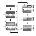
- FIG. 3 is a process view schematically showing the method of FIG. 2
- a plated substrate 10 is provided (step a).
- the substrate may be made of glass, stainless steel or polyimide, and preferably glass.
- the substrate may be sequentially washed with acetone, methanol and distilled water, and then ultrasonically treated.
- first and second molybdenum electrodes 22 and 24 are formed on the substrate (step b).
- the first and second molybdenum electrodes 22 and 24 are formed by depositing a molybdenum layer 20 on the substrate 10 and then patterning the molybdenum layer 20.
- the deposition of the molybdenum layer 10 may is preformed by sputtering. That is, the molybdenum layer 20 may be formed by performing a sputtering process for 1 ⁇ 30 minutes under the conditions of a power of 0.5 ⁇ 50 kW, a sputtering pressure of 0.1 ⁇ 50 m Torr and an argon (Ar) gas supply of 1 ⁇ 100 sccm.
- the deposited molybdenum layer 20, as shown in FIG. 3 is separated into the first molybdenum electrode 22 and the second molybdenum electrode 24 by patterning.
- the first molybdenum electrode 22 and the second molybdenum electrode 24 are disposed at a predetermined interval, and the substrate 10 is exposed by the interval.
- the patterning of the molybdenum layer 10 may be performed by laser scribing.
- the laser scribing may be performed under the conditions of a laser wavelength of 300 ⁇ 1100 nm and a laser power of 0.3 ⁇ 3 W.
- a TCO layer 30 is formed (step c).
- an N-type transparent conducting film and an I-type transparent conducting film are sequentially deposited and patterned on the substrate 10 provided with the first and second molybdenum electrodes 22 and 24 to form a double TCO layer 30.
- each of the N-type and I-type transparent conducting films may be made of zinc oxide, and, if necessary, may be made of ITO.
- each of the N-type and I-type transparent conducting films may be performed by sputtering.
- the N-type transparent conducting film may be formed by performing a sputtering process for 10 ⁇ 100 minutes under the conditions of a power of 50 ⁇ 500 W, a sputtering pressure of 1 ⁇ 50 m Torr, an argon gas supply of 10 ⁇ 100 sccm and an oxygen gas supply of 0.5 ⁇ 10 sccm.
- the I-type transparent conducting film may be formed by performing a sputtering process for 10 ⁇ 100 minutes under the conditions of a power of 50 ⁇ 500 W, a sputtering pressure of 1 ⁇ 50 m Torr and an argon gas supply of 10 ⁇ 100 sccm.
- the N-type and I-type transparent conducting films are sequentially sputtering-deposited and patterned to allow the double TCO layer 30 to be disposed on the upper and lateral sides of the second molybdenum electrode 24 such that the second molybdenum electrode 24 is covered by the double TCO layer 30. Therefore, as shown in FIG. 3 , the double TCO layer 30 and the first molybdenum electrode 22 may be provided on the substrate 10 in parallel with each other at a predetermined interval.
- the pattering of each of the N-type and I-type transparent conducting films may be performed by laser scribing.
- the laser scribing may be performed under the conditions of a laser wavelength of 300 ⁇ 1100 nm and a laser power of 0.3 ⁇ 3 W.
- a buffer layer 40 is formed (step d).
- the buffer layer 40 may be formed by immersing the substrate 10 provided with the first and second molybdenum electrodes 22 and 24 and the TCO layer into a mixed solution including thiourea, cadmium sulfide and ammonia at a temperature of 60 ⁇ 100°C for 10 ⁇ 100 minutes. If necessary, an alternative material such as zinc sulfide, indium sulfide or the like may be used instead of cadmium sulfide.
- the formed buffer layer 40 is patterned such that the buffer layer 40 is spaced apart from the first molybdenum electrode 22 and is disposed on only the upper and lateral sides of the TCO layer 30.
- the patterning of the buffer layer 40 may be performed by laser scribing.
- the laser scribing may be performed under the conditions of a laser wavelength of 300 ⁇ 600 nm and a laser power of 0.3 ⁇ 3 W.
- a light-absorbing layer 50 is formed on the substrate having passed the step d) (step e).
- the light-absorbing layer 50 is made of a CIS-based or CIGS-based compound. Since the CIS-based and CIGS-based compounds were afore-mentioned in the structure of the CIS/CIGS-base solar cell of the present invention, description thereof will be omitted.
- the formation of the light-absorbing layer 50 may be preformed by non-vacuum coating or vacuum coating.
- non-vacuum coating various types of coating methods commonly known in the related field, such as spraying, ultrasonic spraying, spin coating, a doctor blade method, screen printing and ink-jet printing and the like may be used.
- vacuum coating simultaneous vacuum evaporation, sputtering/selenization, three-stage simultaneous vacuum evaporation or the like may be used.
- the simultaneous vacuum evaporation is a process of simultaneously evaporating Cu, In, Ga and Se as starting materials
- the sputtering/selenization is a process of simultaneously sputtering Cu, In, Ga and the like to form a precursor layer and then heat-treating the precursor layer with selenium under a selenium (Sn) atmosphere.
- the three-stage simultaneous vacuum evaporation is a process of evaporating In, Ga and Se at low substrate temperature to form a precursor, supplying Cu to the precursor and then supplying In and Ga to the precursor.
- This light-absorbing layer 50 is formed such that it entirely covers the substrate 10 provided thereon with the first molybdenum electrode 22 and the buffer layer 40.
- an antireflection layer 60 is formed on the light-absorbing layer 50 (step f).
- the antireflection layer is formed by sequentially forming a lower alumina layer and an upper magnesium fluoride layer.
- the alumina layer may be formed by performing ALD (atomic layer deposition) using gas produced by the reaction of trimethyl aluminum (Al(CH) 3 ) and ozone (O 3 ).
- ALD atomic layer deposition
- the magnesium fluoride layer may be formed by performing thermal evaporation using magnesium fluoride pellets.
- a glass substrate having a thickness of 1.1 mm and a size of 10 X 10 cm 2 was sequentially washed with acetone, methanol and distilled water, and was then ultrasonically treated for 15 minutes.
- molybdenum was deposited on the glass substrate for 10 minutes by sputtering under the conditions of a power of 1.4 kW, a sputtering pressure of 10 m Torr, an argon gas supply of 40 sccm to form a molybdenum electrode layer having a thickness of 2 ⁇ m.
- the molybdenum electrode layer was patterned by laser scribing under the conditions of a laser wavelength of 1064 nm and a laser power of 3 W to be separated into a first molybdenum electrode and a second molybdenum electrode. The remaining portion of the molybdenum electrode layer was disposed such that the glass substrate was exposed.
- N-type zinc oxide and I-type zinc oxide were sequentially sputtered and scribed on the glass substrate provided with the molybdenum electrode layer to form a double TCO layer on the exposed surface of the second molybdenum electrode
- the N-type zinc oxide film was formed to a thickness of 0.7 ⁇ m by sputtering N-type zinc oxide for 45 minutes under the conditions of a power of 50 W, a sputtering pressure of 10 m Torr, an argon gas supply of 40 sccm and an oxygen gas supply of 5 sccm. Thereafter, this N-type zinc oxide film was laser-scribed under the conditions of a laser wavelength of 1064 nm and a laser power of 1 W to be patterned such that it is spaced apart from the first molybdenum electrode and covers only the surface of the second molybdenum electrode.
- the I-type zinc oxide film was formed to a thickness of 0.05 ⁇ m by sputtering I-type zinc oxide for 40 minutes under the conditions of a power of 400 W, a sputtering pressure of 1 m Torr and an argon gas supply of 40 sccm. Thereafter, this I-type zinc oxide film was laser-scribed under the conditions of a laser wavelength of 1064 nm and a laser power of 1 W to be patterned such that it covers the upper and lateral surfaces of the N-type zinc oxide film spaced apart from the first molybdenum electrode and covering the upper and lateral surfaces of the second molybdenum electrode.
- the glass substrate provided with the exposed first molybdenum electrode and TCO layer was immersed into a mixed solution including thiourea, cadmium sulfide and ammonia at a temperature of 80°C for 15 minutes to form a cadmium sulfide buffer layer, and then this buffer layer was laser-scribed under the conditions of a laser wavelength of 532 nm and a laser power of 0.3 W to be patterned such that it is spaced apart from the first molybdenum electrode and is disposed only the upper and lateral surfaces of the TCO layer.
- the substrate having passed through the above processes was coated with a solution including Cu, In, Ga and Se nanoparticles by a doctor blade method, and was then heat-treated to form a light-absorbing layer.
- the light-absorbing layer covers the first molybdenum electrode, the buffer layer and the substrate exposed between the first molybdenum electrode and the buffer layer.
- an alumina layer was formed on the light-absorbing layer by performing atomic layer deposition (ALD) using gas produced by the reaction of trimethyl aluminum and ozone, and then a magnesium fluoride layer was formed by thermal evaporation using magnesium fluoride pellets.
- ALD atomic layer deposition
- an embodiment of the present invention is configured such that a TCO layer and a buffer layer is formed on a second molybdenum electrode, this configuration is devised to meet the convenience of explaining the structure of the solar cell of the present invention, the TCO layer and buffer layer may be disposed on any one of molybdenum electrodes, and the arrangement of the molybdenum electrodes may be performed in various manners within the scope of the present invention.
Landscapes
- Photovoltaic Devices (AREA)
Abstract
Description
- The present invention relates to a solar cell, and, more particularly, to a CIS/CIGS-based solar cell including a rear TCO layer at the rear side thereof, which can increase a power generation efficiency by disposing a TCO layer and a buffer layer at the rear side thereof to increase the efficiency of a light-absorbing layer, and to a method of manufacturing the same.
- Recently, due to the problems of serious environmental pollution and fossil energy resource exhaustion, the importance of development of next-generation clean energy sources has increased. Among the next-generation clean energy sources, a solar cell, which is a device for directly converting solar energy into electrical energy, is an energy source that is expected to solve future energy problems because it rarely causes environmental pollution, its energy resource is unrestricted, and its life span is semipermanent.
- Solar cells are classified into various types according to the kind of materials used for a light-absorbing layer. Currently, among these solar cells, a silicon solar cell is generally used. However, the raw material consumption of the thin film-type solar cell is low because it is thin. Further, the thin film-type solar cell can be widely used because it is light. Research into amorphous silicon, Cd-Te, CIS and CIGS, as raw materials of such a thin film-type solar cell, is actively being conducted.
- A CIS thin film or a CIGS thin film is one of I-III-VI compound semiconductors. Among experimentally-made thin film solar cells, a CIS thin film solar cell or a CIGS thin film solar cell exhibits the highest conversion efficiency. Particularly, since a CIS thin film solar cell or a CIGS thin film solar cell can be manufactured to a thickness of 10 µm or less and is stable even when it is used for a long period of time, it is considered as a high-efficiency solar cell that can be used in place of a silicon solar cell.
-
FIG. 3 shows the structure of a conventional CIS/CIGS-based solar cell employing the CIS or CIGS as a light-absorbing layer. - Referring to
FIG. 3 , the conventional CIS/CIGS-based solar cell including a substrate 1, a molybdenum (Mo)electrode 2, a light-absorbinglayer 3, abuffer layer 4, a transparent conducting oxide (TCO)layer 5 and ametal electrode 6, which are sequentially layered from the bottom thereof. - The conventional CIS/CIGS-based solar cell is problematic in that the amount of light incident upon the light-absorbing
layer 3 can be reduced due to the light absorption of thebuffer layer 4 disposed on the light-absorbinglayer 4. Further, the conventional CIS/CIGS-based solar cell is problematic in that its energy conversion efficiency is decreased because themetal electrode 6 is disposed on theTCO layer 5 in the form of a grid to reduce the amount of incident light with respect to the area thereof. - Accordingly, the present invention has been devised to solve the above problems, and an object of the present invention is to provide a solar cell, in which a buffer layer and a TCO layer are disposed at the rear side of a light-absorbing layer, so the amount of light incident on the light-absorbing layer is increased, thereby increasing the energy conversion efficiency of the solar cell.
- In order to accomplish the above object, an aspect of the present invention provides a CIS/CIGS-based solar cell, including: a substrate; first and second molybdenum electrodes disposed on the substrate at a predetermined interval in parallel with each other; a TCO layer disposed on upper and lateral sides of the second molybdenum electrode; a buffer layer disposed on upper and lateral sides of the TCO layer to compensate for a difference in bandgap between the TCO layer and a light-absorbing layer; the light-absorbing layer disposed on the first molybdenum electrode, the buffer layer and an area of the substrate partially opened between the first molybdenum electrode and the buffer layer; and an antireflection layer disposed on the light-absorbing layer to minimize the reflection of externally-applied light.
- The substrate may be made of any one selected from among glass, stainless steel and polyimide.
- The TCO layer may include an N-type lower transparent conducting film and an I-type upper transparent conducting film.
- The TCO layer may be made of zinc oxide or ITO.
- The buffer layer may be made of any one selected from among cadmium sulfide, zinc sulfide and indium sulfide.
- The light-absorbing layer may be made of any one CIS/CIGS-based compound selected from the group consisting of Cu-In-Se, Cu-In-S, Cu-Ga-S, Cu-Ga-Se, Cu-In-Ga-Se, Cu-In-Ga-Se-(S,Se), Cu-In-Al-Ga-(S,Se) and Cu-In-Al-Ga-Se-S, or may be made of any one CZTS-based compound selected from the group consisting of Cu-Zn-Sn-(Se,S) and Cu-In-Ga-Zn-Sn-(Se,S).
- The antireflection layer may include a lower alumina layer in contact with the light-absorbing layer and an upper magnesium fluoride layer exposed to air.
- Another aspect of the present invention provides a method of manufacturing a CIS/CIGS-based solar cell, including the steps of: a) providing a substrate; b) depositing a molybdenum layer on the substrate and then patterning the molybdenum layer to form first and second molybdenum electrodes disposed on the substrate at a predetermined interval in parallel with each other; c) depositing a TCO layer on the substrate having passed through the step b) and then patterning the TCO layer to form a TCO layer disposed on upper and lateral sides of the second molybdenum electrode; d) depositing a buffer layer on the substrate having passed through the step c) and then patterning the buffer layer to form a buffer layer disposed on upper and lateral sides of the TCO layer; e) forming a light-absorbing layer on the substrate having passed through the step d); and f) forming an antireflection layer on the light-absorbing layer.
- The substrate may be made of any one selected from among glass, stainless steel and polyimide.
- The substrate may be provided by sequentially washing it with acetone, methanol and distilled water and then ultrasonically treating it.
- In the step b), the deposition of the molybdenum layer may be preformed by sputtering.
- The deposition of the molybdenum layer using sputtering may be performed for 1 ∼ 30 minutes under the conditions of a power of 0.5 ~ 50 kW, a sputtering pressure of 0.1 ~ 50 m Torr and an argon (Ar) gas supply of 1 ~ 100 sccm.
- In the step b), the patterning of the molybdenum layer may be preformed by laser scribing.
- The patterning of the molybdenum layer using laser scribing may be performed under the conditions of a laser wavelength of 300 ~ 1100 nm and a laser power of 0.3 ~ 3 W.
- The TCO layer is made of zinc oxide or ITO.
- In the step c), the deposition of the TCO layer may be preformed by sputtering.
- In the step c), the patterning of the TCO layer may be preformed by laser scribing.
- The patterning of the TCO layer using laser scribing may be performed under the conditions of a laser wavelength of 300 ~ 1100 nm and a laser power of 0.3 ∼ 3 W.
- In the step c), the TCO layer is formed such a way that an N-type transparent conducting film may be deposited and patterned, and then an I-type transparent conducting film may be deposited and patterned to form a double TCO layer.
- The N-type transparent conducting film and the I-type transparent conducting film may be deposited by sputtering, the deposition of the N-type transparent conducting film using sputtering may be performed for 10 ∼ 100 minutes under the conditions of a power of 50 ∼ 500 W, a sputtering pressure of 1 ∼ 50 m Torr, an argon gas supply of 10 ∼ 100 sccm and an oxygen gas supply of 0.5 ∼ 10 sccm, and the deposition of the I-type transparent conducting film using sputtering may be performed for 10 ~ 100 minutes under the conditions of a power of 50 ~ 500 W, a sputtering pressure of 1 ~ 50 m Torr and an argon gas supply of 10 ~ 100 sccm.
- In the step d), the buffer layer may be made of any one selected from cadmium sulfide, zinc sulfide and indium sulfide.
- In the step d), the buffer layer may be formed by immersing the substrate having passed through the step c) into a mixed solution including thiourea, cadmium sulfide and ammonia.
- The buffer layer may be formed by immersing the substrate into the mixed solution at a temperature of 60 ~ 100°C for 10 ~ 100 minutes.
- In the step d), the patterning of the buffer layer may be preformed by laser scribing.
- The patterning of the buffer layer using laser scribing may be performed under the conditions of a laser wavelength of 300 ~ 600 nm and a laser power of 0.3 ~ 3 W.
- In the step e), the formation of the light-absorbing layer may be preformed by non-vacuum coating or vacuum coating.
- The non-vacuum coating may be any one selected from among spraying, ultrasonic spraying, spin coating, a doctor blade method, screen printing and ink-jet printing.
- The vacuum coating is any one selected from among simultaneous vacuum evaporation, sputtering/selenization and three-stage simultaneous vacuum evaporation.
- In the step f), the antireflection layer may be formed by sequentially forming a lower alumina layer and an upper magnesium fluoride layer.
- The formation of the alumina layer may be performed by atomic layer deposition (ALD) using gas produced by the reaction of trimethyl aluminum and ozone.
- The formation of the magnesium fluoride layer may be performed by thermal evaporation using magnesium fluoride pellets.
- Still another aspect of the present invention provides a solar cell module comprising a CIS/CIGS solar cell, the CIS/CIGS solar cell includng: a substrate; first and second molybdenum electrodes disposed on the substrate at a predetermined interval in parallel with each other; a TCO layer disposed on upper and lateral sides of the second molybdenum electrode; a buffer layer disposed on upper and lateral sides of the TCO layer to compensate for a difference in bandgap between the TCO layer and a light-absorbing layer; the light-absorbing layer disposed on the first molybdenum electrode, the buffer layer and an area of the substrate partially opened between the first molybdenum electrode and the buffer layer; and an antireflection layer disposed on the light-absorbing layer to minimize the reflection of externally-applied light.
- According to the solar cell of the present invention, a buffer layer and a TCO layer are disposed at the rear side of a light-absorbing layer to prevent the amount of light incident upon the light-absorbing layer from being reduced by removing the incident light obstruction structure disposed on the light-absorbing layer, so the amount of light incident upon the light-absorbing layer can be maximized, thereby increasing the energy conversion efficiency of the solar cell.
-
-
FIG. 1 is a side sectional view showing the structure of a CIS/CIGS-based solar cell including a TCO layer at the rear side thereof according to the present invention. -
FIG. 2 is a flowchart showing a method of manufacturing a CIS/CIGS-based solar cell including a TCO layer at the rear side thereof according to the present invention. -
FIG. 3 is a schematic view showing a process of manufacturing a CIS/CIGS-based solar cell including a TCO layer at the rear side thereof according to the present invention. -
FIG. 4 is a side sectional view showing the structure of a conventional CIS/CIGS-based solar cell. - First, a CIS/CIGS-based solar cell including a TCO layer at the rear side thereof according to an embodiment of the present invention will be described, and then a method of manufacturing the same will be described.
- Referring to
FIG. 1 , the CIS/CIGS-based solar cell according to an embodiment of the present invention includes asubstrate 10, first andsecond molybdenum electrodes TCO layer 30, abuffer layer 40, a light-absorbinglayer 50 and anantireflection layer 60, which are sequentially layered from the bottom thereof. Here, theTCO layer 30 and thebuffer layer 40 are sequentially disposed on the upper and lateral sides of thesecond molybdenum electrode 24 to be disposed on thesubstrate 10 in parallel with each other and spaced apart from thefirst molybdenum electrode 22. Hereinafter, the structure of the CIS/CIGS-based solar cell will be described in detail. - The
substrate 10 is a plated structure on which components of a solar cell are disposed and which serves to support the components thereof. Preferably, the substrate is made of glass, but, if necessary, may be made of stainless steel, polyimide or the like. - The
first molybdenum electrode 22 and thesecond molybdenum electrode 24 are disposed on thesubstrate 10 in parallel with each other at a predetermined interval. In this case, thefirst molybdenum electrode 22 corresponds to a rear electrode of a general thin film solar cell, and thesecond molybdenum electrode 24 corresponds to a front metal electrode thereof. - The
TCO layer 30 is a transparent conducting layer, and is disposed on the upper and lateral sides of thesecond molybdenum electrode 24 to cover thesecond molybdenum electrode 24. Therefore, thefirst molybdenum electrode 22 and theTCO layer 30 are disposed on thesubstrate 10 in parallel with each other with the light-absorbinglayer 50 being disposed therebetween. - In this case, the
TCO layer 30 consists of a lower layer and an upper layer. The lower layer is an N-type transparent conducting film, and the upper layer is an I-type transparent conducting film. The lower and upper layers can constitute a PIN junction together with the light-absorbinglayer 50. - Here, the
TCO layer 30 may be made of a transparent material having electrical conductivity, such as zinc oxide (ZnO), indium tin oxide (ITO) or the like. - The
buffer layer 40 functions to reduce the increase in bandgap between theTCO layer 30 and the light-absorbinglayer 50. Thebuffer layer 40 is disposed on the upper and lateral sides of theTCO layer 30 to cover theTCO layer 30. It is preferred that thebuffer layer 40 be made of cadmium sulfide (CdS). Thebuffer layer 40 may also be made of an alternative material such as zinc sulfide (ZnS), indium sulfide (In2S3) or the like. , - The light-absorbing
layer 50 is disposed over thefirst molybdenum electrode 22, thebuffer layer 40 and the substrate exposed between thefirst molybdenum electrode 22 and thebuffer layer 40. - The light-absorbing
layer 50 may be made of a CIS-based compound or a CIGS-based compound. Specifically, the light-absorbinglayer 50 may include: ternary compounds such as Cu-InS, Cu-Ga-S, Cu-Ga-Se and the like; quaternary compounds such as Cu-In-Ga-Se and the like; and 5-component and 6-component compounds such as Cu-In-Ga-Se-(S,Se), Cu-In-Al-Ga-(S,Se), Cu-In-Al-Ga-Se-S and the like. These compounds are based on Cu-In-Se which is an IB-IIIA-VIA group semiconductor. - Moreover, the light-absorbing
layer 50 may further include a CZTS-based compound. The CZTS-based compound may include Cu-Zn-Sn-(Se,S) obtained by substituting all IIIA group elements (In, Ga, Al, etc.) with IIB group elements (Zn, etc.) and IVA group elements (Sn, etc.) and Cu-In-Ga-Zn-Sn-(Se,S) obtained by substituting some of IIIA group elements (In, Ga, Al, etc.) with IIB group elements (Zn, etc.) and IVA group elements (Sn, etc.) - The
antireflection layer 60 is disposed on the light-absorbing layer, and is provided as a double layer including a lower alumina (Al2O3) layer in contact with the light-absorbinglayer 50 and an upper magnesium fluoride (MgF2) layer directly exposed to the air. - Therefore, the CIS/CIGS-base solar cell of the present invention is advantageous in that the problem of deterioration of light absorptivity occurring when the
TCO layer 30 and thebuffer layer 40 is disposed at the front of the solar cell can be solved because they are disposed under the light-absorbinglayer 50. - The present invention provides a solar cell module including the CIS/CIGS-based solar cell.
-
FIG. 2 is a flowchart showing a method of manufacturing a CIS/CIGS-based solar cell according to the present invention, andFIG. 3 is a process view schematically showing the method ofFIG. 2 - Hereinafter, the method of manufacturing a CIS/CIGS-based solar cell according to the present invention will be described with reference to
FIGS. 2 and3 . - First, a plated
substrate 10 is provided (step a). - As described in the structure of the CIS/CIGS solar cell, the substrate may be made of glass, stainless steel or polyimide, and preferably glass.
- The substrate may be sequentially washed with acetone, methanol and distilled water, and then ultrasonically treated.
- Thereafter, first and
second molybdenum electrodes - The first and
second molybdenum electrodes molybdenum layer 20 on thesubstrate 10 and then patterning themolybdenum layer 20. Specifically, the deposition of themolybdenum layer 10 may is preformed by sputtering. That is, themolybdenum layer 20 may be formed by performing a sputtering process for 1 ~ 30 minutes under the conditions of a power of 0.5 ~ 50 kW, a sputtering pressure of 0.1 ~ 50 m Torr and an argon (Ar) gas supply of 1 ~ 100 sccm. - The deposited
molybdenum layer 20, as shown inFIG. 3 , is separated into thefirst molybdenum electrode 22 and thesecond molybdenum electrode 24 by patterning. Thefirst molybdenum electrode 22 and thesecond molybdenum electrode 24 are disposed at a predetermined interval, and thesubstrate 10 is exposed by the interval. - The patterning of the
molybdenum layer 10 may be performed by laser scribing. The laser scribing may be performed under the conditions of a laser wavelength of 300 ~ 1100 nm and a laser power of 0.3 ~ 3 W. - Subsequently, a
TCO layer 30 is formed (step c). - Specifically, an N-type transparent conducting film and an I-type transparent conducting film are sequentially deposited and patterned on the
substrate 10 provided with the first andsecond molybdenum electrodes double TCO layer 30. Here, each of the N-type and I-type transparent conducting films may be made of zinc oxide, and, if necessary, may be made of ITO. - The deposition of each of the N-type and I-type transparent conducting films may be performed by sputtering.
- In this case, the N-type transparent conducting film may be formed by performing a sputtering process for 10 ~ 100 minutes under the conditions of a power of 50 ~ 500 W, a sputtering pressure of 1 ~ 50 m Torr, an argon gas supply of 10 ~ 100 sccm and an oxygen gas supply of 0.5 ~ 10 sccm.
- Further, the I-type transparent conducting film may be formed by performing a sputtering process for 10 ~ 100 minutes under the conditions of a power of 50 ~ 500 W, a sputtering pressure of 1 ~ 50 m Torr and an argon gas supply of 10 ~ 100 sccm.
- The N-type and I-type transparent conducting films are sequentially sputtering-deposited and patterned to allow the
double TCO layer 30 to be disposed on the upper and lateral sides of thesecond molybdenum electrode 24 such that thesecond molybdenum electrode 24 is covered by thedouble TCO layer 30. Therefore, as shown inFIG. 3 , thedouble TCO layer 30 and thefirst molybdenum electrode 22 may be provided on thesubstrate 10 in parallel with each other at a predetermined interval. - The pattering of each of the N-type and I-type transparent conducting films may be performed by laser scribing. The laser scribing may be performed under the conditions of a laser wavelength of 300 ~ 1100 nm and a laser power of 0.3 ~ 3 W.
- Subsequently, a
buffer layer 40 is formed (step d). - Specifically, the
buffer layer 40 may be formed by immersing thesubstrate 10 provided with the first andsecond molybdenum electrodes - Then, the formed
buffer layer 40 is patterned such that thebuffer layer 40 is spaced apart from thefirst molybdenum electrode 22 and is disposed on only the upper and lateral sides of theTCO layer 30. The patterning of thebuffer layer 40 may be performed by laser scribing. The laser scribing may be performed under the conditions of a laser wavelength of 300 ~ 600 nm and a laser power of 0.3 ~ 3 W. - Subsequently, a light-absorbing
layer 50 is formed on the substrate having passed the step d) (step e). - The light-absorbing
layer 50 is made of a CIS-based or CIGS-based compound. Since the CIS-based and CIGS-based compounds were afore-mentioned in the structure of the CIS/CIGS-base solar cell of the present invention, description thereof will be omitted. - The formation of the light-absorbing
layer 50 may be preformed by non-vacuum coating or vacuum coating. As the non-vacuum coating, various types of coating methods commonly known in the related field, such as spraying, ultrasonic spraying, spin coating, a doctor blade method, screen printing and ink-jet printing and the like may be used. - Further, as the vacuum coating, simultaneous vacuum evaporation, sputtering/selenization, three-stage simultaneous vacuum evaporation or the like may be used.
- Here, the simultaneous vacuum evaporation is a process of simultaneously evaporating Cu, In, Ga and Se as starting materials, and the sputtering/selenization is a process of simultaneously sputtering Cu, In, Ga and the like to form a precursor layer and then heat-treating the precursor layer with selenium under a selenium (Sn) atmosphere. Further, the three-stage simultaneous vacuum evaporation is a process of evaporating In, Ga and Se at low substrate temperature to form a precursor, supplying Cu to the precursor and then supplying In and Ga to the precursor.
- This light-absorbing
layer 50 is formed such that it entirely covers thesubstrate 10 provided thereon with thefirst molybdenum electrode 22 and thebuffer layer 40. - Finally, an
antireflection layer 60 is formed on the light-absorbing layer 50 (step f). - In this case, the antireflection layer is formed by sequentially forming a lower alumina layer and an upper magnesium fluoride layer.
- The alumina layer may be formed by performing ALD (atomic layer deposition) using gas produced by the reaction of trimethyl aluminum (Al(CH)3) and ozone (O3).
- Further, the magnesium fluoride layer may be formed by performing thermal evaporation using magnesium fluoride pellets.
- Hereinafter, the method of manufacturing a CIS/CIGS-based solar cell according to the present invention will be described in detail with reference to the following Example.
- A glass substrate having a thickness of 1.1 mm and a size of 10 X 10 cm2 was sequentially washed with acetone, methanol and distilled water, and was then ultrasonically treated for 15 minutes.
- Thereafter, molybdenum was deposited on the glass substrate for 10 minutes by sputtering under the conditions of a power of 1.4 kW, a sputtering pressure of 10 m Torr, an argon gas supply of 40 sccm to form a molybdenum electrode layer having a thickness of 2 µm. Subsequently, the molybdenum electrode layer was patterned by laser scribing under the conditions of a laser wavelength of 1064 nm and a laser power of 3 W to be separated into a first molybdenum electrode and a second molybdenum electrode. The remaining portion of the molybdenum electrode layer was disposed such that the glass substrate was exposed.
- Subsequently, N-type zinc oxide and I-type zinc oxide were sequentially sputtered and scribed on the glass substrate provided with the molybdenum electrode layer to form a double TCO layer on the exposed surface of the second molybdenum electrode
- The N-type zinc oxide film was formed to a thickness of 0.7 µm by sputtering N-type zinc oxide for 45 minutes under the conditions of a power of 50 W, a sputtering pressure of 10 m Torr, an argon gas supply of 40 sccm and an oxygen gas supply of 5 sccm. Thereafter, this N-type zinc oxide film was laser-scribed under the conditions of a laser wavelength of 1064 nm and a laser power of 1 W to be patterned such that it is spaced apart from the first molybdenum electrode and covers only the surface of the second molybdenum electrode.
- The I-type zinc oxide film was formed to a thickness of 0.05 µm by sputtering I-type zinc oxide for 40 minutes under the conditions of a power of 400 W, a sputtering pressure of 1 m Torr and an argon gas supply of 40 sccm. Thereafter, this I-type zinc oxide film was laser-scribed under the conditions of a laser wavelength of 1064 nm and a laser power of 1 W to be patterned such that it covers the upper and lateral surfaces of the N-type zinc oxide film spaced apart from the first molybdenum electrode and covering the upper and lateral surfaces of the second molybdenum electrode.
- Subsequently, the glass substrate provided with the exposed first molybdenum electrode and TCO layer was immersed into a mixed solution including thiourea, cadmium sulfide and ammonia at a temperature of 80°C for 15 minutes to form a cadmium sulfide buffer layer, and then this buffer layer was laser-scribed under the conditions of a laser wavelength of 532 nm and a laser power of 0.3 W to be patterned such that it is spaced apart from the first molybdenum electrode and is disposed only the upper and lateral surfaces of the TCO layer.
- Thereafter, the substrate having passed through the above processes was coated with a solution including Cu, In, Ga and Se nanoparticles by a doctor blade method, and was then heat-treated to form a light-absorbing layer. The light-absorbing layer covers the first molybdenum electrode, the buffer layer and the substrate exposed between the first molybdenum electrode and the buffer layer.
- Finally, an alumina layer was formed on the light-absorbing layer by performing atomic layer deposition (ALD) using gas produced by the reaction of trimethyl aluminum and ozone, and then a magnesium fluoride layer was formed by thermal evaporation using magnesium fluoride pellets.
- Although the preferred embodiments of the present invention have been disclosed for illustrative purposes, those skilled in the art will appreciate that various modifications, additions and substitutions are possible, without departing from the scope and spirit of the invention as disclosed in the accompanying claims.
- For example, although an embodiment of the present invention is configured such that a TCO layer and a buffer layer is formed on a second molybdenum electrode, this configuration is devised to meet the convenience of explaining the structure of the solar cell of the present invention, the TCO layer and buffer layer may be disposed on any one of molybdenum electrodes, and the arrangement of the molybdenum electrodes may be performed in various manners within the scope of the present invention.
Claims (32)
- A CIS/CIGS-based solar cell, comprising:a substrate;first and second molybdenum electrodes disposed on the substrate at a predetermined interval in parallel with each other;a TCO layer disposed on upper and lateral sides of the second molybdenum electrode;a buffer layer disposed on upper and lateral sides of the TCO layer to compensate for a difference in bandgap between the TCO layer and a light-absorbing layer;the light-absorbing layer disposed on the first molybdenum electrode, the buffer layer and an area of the substrate partially opened between the first molybdenum electrode and the buffer layer; andan antireflection layer disposed on the light-absorbing layer to minimize the reflection of externally-applied light.
- The CIS/CIGS-based solar cell of claim 1, wherein the substrate is made of any one selected from among glass, stainless steel and polyimide.
- The CIS/CIGS-based solar cell of claim 1, wherein the TCO layer includes an N-type lower transparent conducting film and an I-type upper transparent conducting film.
- The CIS/CIGS-based solar cell of claim 1, wherein the TCO layer is made of zinc oxide or ITO.
- The CIS/CIGS-based solar cell of claim 1, wherein the buffer layer is made of any one selected from among cadmium sulfide, zinc sulfide and indium sulfide.
- The CIS/CIGS-based solar cell of claim 1, wherein the light-absorbing layer is made of any one CIS/CIGS-based compound selected from the group consisting of Cu-In-Se, Cu-In-S, Cu-Ga-S, Cu-Ga-Se, Cu-In-Ga-Se, Cu-In-Ga-Se-(S,Se), Cu-In-Al-Ga-(S,Se) and Cu-In-Al-Ga-Se-S, or is made of any one CZTS-based compound selected from the group consisting of Cu-Zn-Sn-(Se,S) and Cu-In-Ga-Zn-Sn-(Se,S).
- The CIS/CIGS-based solar cell of claim 1, wherein the antireflection layer includes a lower alumina layer in contact with the light-absorbing layer and an upper magnesium fluoride layer exposed to air.
- A method of manufacturing a CIS/CIGS-based solar cell, comprising the steps of:a) providing a substrate;b) depositing a molybdenum layer on the substrate and then patterning the molybdenum layer to form first and second molybdenum electrodes disposed on the substrate at a predetermined interval in parallel with each other;c) depositing a TCO layer on the substrate having passed through the step b) and then patterning the TCO layer to form a TCO layer disposed on upper and lateral sides of the second molybdenum electrode;d) depositing a buffer layer on the substrate having passed through the step c) and then patterning the buffer layer to form a buffer layer disposed on upper and lateral sides of the TCO layer;e) forming a light-absorbing layer on the substrate having passed through the step d); andf) forming an antireflection layer on the light-absorbing layer.
- The method of claim 8, wherein the substrate is made of any one selected from among glass, stainless steel and polyimide.
- The method of claim 8, wherein the substrate is provided by sequentially washing it with acetone, methanol and distilled water and then ultrasonically treating it.
- The method of claim 8, wherein, in the step b), the deposition of the molybdenum layer is preformed by sputtering.
- The method of claim 11, wherein the deposition of the molybdenum layer using sputtering is performed for 1 ∼ 30 minutes under the conditions of a power of 0.5 ~ 50 kW, a sputtering pressure of 0.1 ~ 50 m Torr and an argon (Ar) gas supply of 1 ∼ 100 sccm.
- The method of claim 8, wherein, in the step b), the patterning of the molybdenum layer is preformed by laser scribing.
- The method of claim 13, wherein the patterning of the molybdenum layer using laser scribing is performed under the conditions of a laser wavelength of 300 ~ 1100 nm and a laser power of 0.3 ~ 3 W.
- The method of claim 8, wherein the TCO layer is made of zinc oxide or ITO.
- The method of claim 8, wherein, in the step c), the deposition of the TCO layer is preformed by sputtering.
- The method of claim 8, wherein, in the step c), the patterning of the TCO layer is preformed by laser scribing.
- The method of claim 17, wherein the patterning of the TCO layer using laser scribing is performed under the conditions of a laser wavelength of 300 ~ 1100 nm and a laser power of 0.3 ~ 3 W.
- The method of claim 8, wherein, in the step c), the TCO layer is formed such a way that an N-type transparent conducting film is deposited and patterned, and then an I-type transparent conducting film is deposited and patterned to form a double TCO layer.
- The method of claim 19, wherein the N-type transparent conducting film and the I-type transparent conducting film are deposited by sputtering,
the deposition of the N-type transparent conducting film using sputtering is performed for 10 ~ 100 minutes under the conditions of a power of 50 ~ 500 W, a sputtering pressure of 1 ∼ 50 m Torr, an argon gas supply of 10 ~ 100 sccm and an oxygen gas supply of 0.5 ~ 10 sccm, and
the deposition of the I-type transparent conducting film using sputtering is performed for 10 ~ 100 minutes under the conditions of a power of 50 ~ 500 W, a sputtering pressure of 1 ∼ 50 m Torr and an argon gas supply of 10 ~ 100 sccm. - The method of claim 8, wherein, in the step d), the buffer layer is made of any one selected from cadmium sulfide, zinc sulfide and indium sulfide.
- The method of claim 8, wherein, in the step d), the buffer layer is formed by immersing the substrate having passed through the step c) into a mixed solution including thiourea, cadmium sulfide and ammonia.
- The method of claim 22, wherein the buffer layer is formed by immersing the substrate into the mixed solution at a temperature of 60 ~ 100°C for 10 ~ 100 minutes.
- The method of claim 8, wherein, in the step d), the patterning of the buffer layer is preformed by laser scribing.
- The method of claim 24, wherein the patterning of the buffer layer using laser scribing is performed under the conditions of a laser wavelength of 300 ~ 600 nm and a laser power of 0.3 ~ 3 W.
- The method of claim 8, wherein, in the step e), the formation of the light-absorbing layer is preformed by non-vacuum coating or vacuum coating.
- The method of claim 26, wherein the non-vacuum coating is any one selected from among spraying, ultrasonic spraying, spin coating, a doctor blade method, screen printing and ink-jet printing.
- The method of claim 26, wherein the vacuum coating is any one selected from among simultaneous vacuum evaporation, sputtering/selenization and three-stage simultaneous vacuum evaporation.
- The method of claim 8, wherein, in the step f), the antireflection layer is formed by sequentially forming a lower alumina layer and an upper magnesium fluoride layer.
- The method of claim 29, wherein the formation of the alumina layer is performed by atomic layer deposition (ALD) using gas'produced by the reaction of trimethyl aluminum and ozone.
- The method of claim 29, wherein the formation of the magnesium fluoride layer is performed by thermal evaporation using magnesium fluoride pellets.
- A solar cell module comprising a CIS/CIGS solar cell, the CIS/CIGS solar cell comprising:a substrate;first and second molybdenum electrodes disposed on the substrate at a predetermined interval in parallel with each other;a TCO layer disposed on upper and lateral sides of the second molybdenum electrode;a buffer layer disposed on upper and lateral sides of the TCO layer to compensate for a difference in bandgap between the TCO layer and a light-absorbing layer;the light-absorbing layer disposed on the first molybdenum electrode, the buffer layer and an area of the substrate partially opened between the first molybdenum electrode and the buffer layer; andan antireflection layer disposed on the light-absorbing layer to minimize the reflection of externally-applied light.
Applications Claiming Priority (2)
| Application Number | Priority Date | Filing Date | Title |
|---|---|---|---|
| KR1020110122499A KR101230973B1 (en) | 2011-11-22 | 2011-11-22 | Cis/cigs based-thin film solar cell having back side tco layer and method for manufacturing the same |
| PCT/KR2012/008376 WO2013077547A1 (en) | 2011-11-22 | 2012-10-15 | Cis/cigs solar cell having a rear tco layer and production method therefor |
Publications (3)
| Publication Number | Publication Date |
|---|---|
| EP2784829A1 true EP2784829A1 (en) | 2014-10-01 |
| EP2784829A4 EP2784829A4 (en) | 2015-08-26 |
| EP2784829B1 EP2784829B1 (en) | 2018-05-16 |
Family
ID=47899112
Family Applications (1)
| Application Number | Title | Priority Date | Filing Date |
|---|---|---|---|
| EP12852335.4A Active EP2784829B1 (en) | 2011-11-22 | 2012-10-15 | Cis/cigs solar cell having a rear tco layer and production method therefor |
Country Status (4)
| Country | Link |
|---|---|
| EP (1) | EP2784829B1 (en) |
| KR (1) | KR101230973B1 (en) |
| CN (1) | CN103477442B (en) |
| WO (1) | WO2013077547A1 (en) |
Families Citing this family (11)
| Publication number | Priority date | Publication date | Assignee | Title |
|---|---|---|---|---|
| KR101405113B1 (en) * | 2013-03-12 | 2014-06-11 | 한국에너지기술연구원 | Solar Cell with Back-Side Buffer Layer and its Fabrication Method. |
| KR101394181B1 (en) * | 2013-04-22 | 2014-05-15 | 한국에너지기술연구원 | Flexible solar cell with back-side buffer layer. |
| KR101467462B1 (en) * | 2013-05-03 | 2014-12-02 | (주) 다쓰테크 | Manufacturing method of thin film solar cells |
| CN104253167A (en) * | 2013-06-27 | 2014-12-31 | 海洋王照明科技股份有限公司 | Solar cell device and production method thereof |
| CN103354252B (en) * | 2013-07-17 | 2015-07-29 | 深圳先进技术研究院 | The PN junction of CZTS solar cell and the preparation method of CZTS solar cell device |
| KR101497955B1 (en) * | 2013-07-25 | 2015-03-03 | 한국에너지기술연구원 | Light transmitting back contact and solar cell using the same, and methods of manufacturing them |
| CN104425645B (en) * | 2013-08-30 | 2016-08-24 | 大族激光科技产业集团股份有限公司 | CIGS thin film solaode stays the method on the clear limit of Mo |
| KR20150031889A (en) * | 2013-09-17 | 2015-03-25 | 엘지이노텍 주식회사 | Solar cell |
| KR101924538B1 (en) | 2017-09-14 | 2019-02-22 | 한국과학기술연구원 | Chalcogenide solar cell having a transparent conductive oxide back electrode and method for manufacturing the same |
| CN107651864A (en) * | 2017-11-13 | 2018-02-02 | 苏州安洁科技股份有限公司 | A kind of technique for adding anti-fog performance after glass physical vapour deposition anti-reflection film |
| CN119069551B (en) * | 2024-11-04 | 2025-01-28 | 内蒙古大学 | CZTSSe thin film solar cell and preparation method thereof |
Family Cites Families (11)
| Publication number | Priority date | Publication date | Assignee | Title |
|---|---|---|---|---|
| WO2002021602A1 (en) * | 2000-09-08 | 2002-03-14 | Akzo Nobel N.V. | Colored solar cell unit |
| CN101521249B (en) * | 2002-09-30 | 2012-05-23 | 米亚索尔公司 | Manufacturing apparatus and method for large-scale production of thin-film solar cells |
| JP2007123532A (en) * | 2005-10-27 | 2007-05-17 | Honda Motor Co Ltd | Solar cell |
| KR101372536B1 (en) * | 2007-10-02 | 2014-03-18 | 엘지전자 주식회사 | Tandem Thin Film Solar Cell And Fabrication Method Thereof |
| KR101013326B1 (en) * | 2008-11-28 | 2011-02-09 | 한국광기술원 | CIS-based solar cell and its manufacturing method |
| JP4550928B2 (en) * | 2009-01-16 | 2010-09-22 | 富士フイルム株式会社 | Photoelectric conversion element and solar cell using the same |
| CN102449780B (en) * | 2009-03-31 | 2015-08-05 | Lg伊诺特有限公司 | Solar battery apparatus and manufacture method thereof |
| US20100326520A1 (en) * | 2009-06-29 | 2010-12-30 | Auria Solar Co., Ltd. | Thin film solar cell and manufacturing method thereof |
| KR20110015998A (en) * | 2009-08-10 | 2011-02-17 | 삼성전자주식회사 | Solar cell and manufacturing method thereof |
| KR101306913B1 (en) * | 2009-09-02 | 2013-09-10 | 한국전자통신연구원 | Solar Cell |
| KR101103770B1 (en) * | 2009-10-12 | 2012-01-06 | 이화여자대학교 산학협력단 | Compound Semiconductor Solar Cells and Manufacturing Method Thereof |
-
2011
- 2011-11-22 KR KR1020110122499A patent/KR101230973B1/en not_active Expired - Fee Related
-
2012
- 2012-10-15 CN CN201280012153.7A patent/CN103477442B/en active Active
- 2012-10-15 EP EP12852335.4A patent/EP2784829B1/en active Active
- 2012-10-15 WO PCT/KR2012/008376 patent/WO2013077547A1/en not_active Ceased
Also Published As
| Publication number | Publication date |
|---|---|
| WO2013077547A1 (en) | 2013-05-30 |
| EP2784829A4 (en) | 2015-08-26 |
| CN103477442B (en) | 2016-03-09 |
| KR101230973B1 (en) | 2013-02-07 |
| EP2784829B1 (en) | 2018-05-16 |
| CN103477442A (en) | 2013-12-25 |
Similar Documents
| Publication | Publication Date | Title |
|---|---|---|
| EP2784829B1 (en) | Cis/cigs solar cell having a rear tco layer and production method therefor | |
| US9812593B2 (en) | Solar cell and preparing method of the same | |
| WO2011126454A1 (en) | Thin film photovoltaic solar cells | |
| US20140076392A1 (en) | Solar cell | |
| KR101154786B1 (en) | Solar cell apparatus and method of fabricating the same | |
| KR20090034078A (en) | Tandem thin film solar cell and manufacturing method thereof | |
| KR20110068157A (en) | Cu-In-en-Sn- (Se, S) -based thin film for solar cells and method for manufacturing same | |
| KR101067295B1 (en) | Thin film solar cell and manufacturing method thereof | |
| KR101219835B1 (en) | Solar cell apparatus and method of fabricating the same | |
| US8916411B1 (en) | Absorber layer for a thin film photovoltaic device with a double-graded band gap | |
| KR20170103466A (en) | Solar cell and manufacturing method thereof | |
| KR102925348B1 (en) | Inclined thin film solar cell | |
| US20150027525A1 (en) | Solar cell and preparing method of the same | |
| KR20090100705A (en) | Thin film type positive battery having tandem type of COS-based and CCS-based light absorbing layer and method for manufacturing same | |
| TW201508935A (en) | Photovoltaic device and method of forming photovoltaic device | |
| KR101241708B1 (en) | Solar cell apparatus and method of fabricating the same | |
| KR101382898B1 (en) | See through type solar cell and fabricating method | |
| US20140246073A1 (en) | Solar cell and solar cell module using the same | |
| JP2003008039A (en) | Method for manufacturing compound solar cell | |
| KR101062319B1 (en) | Window manufacturing method using a cell and a cassette used therein | |
| KR20090034079A (en) | Solar cell comprising molybdenum selenide layer and manufacturing method thereof | |
| KR101180998B1 (en) | Solar cell and method of fabricating the same | |
| KR20110116485A (en) | Solar cell manufacturing method | |
| US20150249171A1 (en) | Method of making photovoltaic device comprising i-iii-vi2 compound absorber having tailored atomic distribution | |
| US20140366942A1 (en) | Solar cell and method of fabricating the same |
Legal Events
| Date | Code | Title | Description |
|---|---|---|---|
| PUAI | Public reference made under article 153(3) epc to a published international application that has entered the european phase |
Free format text: ORIGINAL CODE: 0009012 |
|
| 17P | Request for examination filed |
Effective date: 20140520 |
|
| AK | Designated contracting states |
Kind code of ref document: A1 Designated state(s): AL AT BE BG CH CY CZ DE DK EE ES FI FR GB GR HR HU IE IS IT LI LT LU LV MC MK MT NL NO PL PT RO RS SE SI SK SM TR |
|
| DAX | Request for extension of the european patent (deleted) | ||
| RA4 | Supplementary search report drawn up and despatched (corrected) |
Effective date: 20150727 |
|
| RIC1 | Information provided on ipc code assigned before grant |
Ipc: H01L 31/0749 20120101ALI20150721BHEP Ipc: H01L 31/0224 20060101ALI20150721BHEP Ipc: H01L 31/18 20060101AFI20150721BHEP Ipc: H01L 31/02 20060101ALI20150721BHEP Ipc: B23K 26/36 20140101ALI20150721BHEP Ipc: H01L 31/0392 20060101ALI20150721BHEP Ipc: H01L 31/0216 20140101ALI20150721BHEP Ipc: H01L 31/032 20060101ALI20150721BHEP |
|
| GRAP | Despatch of communication of intention to grant a patent |
Free format text: ORIGINAL CODE: EPIDOSNIGR1 |
|
| STAA | Information on the status of an ep patent application or granted ep patent |
Free format text: STATUS: GRANT OF PATENT IS INTENDED |
|
| RIC1 | Information provided on ipc code assigned before grant |
Ipc: H01L 31/18 20060101AFI20171205BHEP Ipc: H01L 31/032 20060101ALI20171205BHEP Ipc: H01L 31/0224 20060101ALI20171205BHEP Ipc: H01L 31/0749 20120101ALI20171205BHEP Ipc: H01L 31/0392 20060101ALI20171205BHEP Ipc: H01L 31/0216 20140101ALI20171205BHEP Ipc: B23K 26/36 20140101ALI20171205BHEP Ipc: H01L 31/02 20060101ALI20171205BHEP |
|
| INTG | Intention to grant announced |
Effective date: 20180104 |
|
| GRAS | Grant fee paid |
Free format text: ORIGINAL CODE: EPIDOSNIGR3 |
|
| GRAA | (expected) grant |
Free format text: ORIGINAL CODE: 0009210 |
|
| STAA | Information on the status of an ep patent application or granted ep patent |
Free format text: STATUS: THE PATENT HAS BEEN GRANTED |
|
| AK | Designated contracting states |
Kind code of ref document: B1 Designated state(s): AL AT BE BG CH CY CZ DE DK EE ES FI FR GB GR HR HU IE IS IT LI LT LU LV MC MK MT NL NO PL PT RO RS SE SI SK SM TR |
|
| REG | Reference to a national code |
Ref country code: GB Ref legal event code: FG4D |
|
| REG | Reference to a national code |
Ref country code: CH Ref legal event code: EP |
|
| REG | Reference to a national code |
Ref country code: IE Ref legal event code: FG4D |
|
| REG | Reference to a national code |
Ref country code: DE Ref legal event code: R096 Ref document number: 602012046492 Country of ref document: DE |
|
| REG | Reference to a national code |
Ref country code: AT Ref legal event code: REF Ref document number: 1000319 Country of ref document: AT Kind code of ref document: T Effective date: 20180615 |
|
| REG | Reference to a national code |
Ref country code: NL Ref legal event code: MP Effective date: 20180516 |
|
| REG | Reference to a national code |
Ref country code: LT Ref legal event code: MG4D |
|
| PG25 | Lapsed in a contracting state [announced via postgrant information from national office to epo] |
Ref country code: NO Free format text: LAPSE BECAUSE OF FAILURE TO SUBMIT A TRANSLATION OF THE DESCRIPTION OR TO PAY THE FEE WITHIN THE PRESCRIBED TIME-LIMIT Effective date: 20180816 Ref country code: FI Free format text: LAPSE BECAUSE OF FAILURE TO SUBMIT A TRANSLATION OF THE DESCRIPTION OR TO PAY THE FEE WITHIN THE PRESCRIBED TIME-LIMIT Effective date: 20180516 Ref country code: LT Free format text: LAPSE BECAUSE OF FAILURE TO SUBMIT A TRANSLATION OF THE DESCRIPTION OR TO PAY THE FEE WITHIN THE PRESCRIBED TIME-LIMIT Effective date: 20180516 Ref country code: ES Free format text: LAPSE BECAUSE OF FAILURE TO SUBMIT A TRANSLATION OF THE DESCRIPTION OR TO PAY THE FEE WITHIN THE PRESCRIBED TIME-LIMIT Effective date: 20180516 Ref country code: SE Free format text: LAPSE BECAUSE OF FAILURE TO SUBMIT A TRANSLATION OF THE DESCRIPTION OR TO PAY THE FEE WITHIN THE PRESCRIBED TIME-LIMIT Effective date: 20180516 Ref country code: BG Free format text: LAPSE BECAUSE OF FAILURE TO SUBMIT A TRANSLATION OF THE DESCRIPTION OR TO PAY THE FEE WITHIN THE PRESCRIBED TIME-LIMIT Effective date: 20180816 |
|
| PG25 | Lapsed in a contracting state [announced via postgrant information from national office to epo] |
Ref country code: LV Free format text: LAPSE BECAUSE OF FAILURE TO SUBMIT A TRANSLATION OF THE DESCRIPTION OR TO PAY THE FEE WITHIN THE PRESCRIBED TIME-LIMIT Effective date: 20180516 Ref country code: NL Free format text: LAPSE BECAUSE OF FAILURE TO SUBMIT A TRANSLATION OF THE DESCRIPTION OR TO PAY THE FEE WITHIN THE PRESCRIBED TIME-LIMIT Effective date: 20180516 Ref country code: RS Free format text: LAPSE BECAUSE OF FAILURE TO SUBMIT A TRANSLATION OF THE DESCRIPTION OR TO PAY THE FEE WITHIN THE PRESCRIBED TIME-LIMIT Effective date: 20180516 Ref country code: GR Free format text: LAPSE BECAUSE OF FAILURE TO SUBMIT A TRANSLATION OF THE DESCRIPTION OR TO PAY THE FEE WITHIN THE PRESCRIBED TIME-LIMIT Effective date: 20180817 Ref country code: HR Free format text: LAPSE BECAUSE OF FAILURE TO SUBMIT A TRANSLATION OF THE DESCRIPTION OR TO PAY THE FEE WITHIN THE PRESCRIBED TIME-LIMIT Effective date: 20180516 |
|
| REG | Reference to a national code |
Ref country code: AT Ref legal event code: MK05 Ref document number: 1000319 Country of ref document: AT Kind code of ref document: T Effective date: 20180516 |
|
| PG25 | Lapsed in a contracting state [announced via postgrant information from national office to epo] |
Ref country code: DK Free format text: LAPSE BECAUSE OF FAILURE TO SUBMIT A TRANSLATION OF THE DESCRIPTION OR TO PAY THE FEE WITHIN THE PRESCRIBED TIME-LIMIT Effective date: 20180516 Ref country code: AT Free format text: LAPSE BECAUSE OF FAILURE TO SUBMIT A TRANSLATION OF THE DESCRIPTION OR TO PAY THE FEE WITHIN THE PRESCRIBED TIME-LIMIT Effective date: 20180516 Ref country code: PL Free format text: LAPSE BECAUSE OF FAILURE TO SUBMIT A TRANSLATION OF THE DESCRIPTION OR TO PAY THE FEE WITHIN THE PRESCRIBED TIME-LIMIT Effective date: 20180516 Ref country code: EE Free format text: LAPSE BECAUSE OF FAILURE TO SUBMIT A TRANSLATION OF THE DESCRIPTION OR TO PAY THE FEE WITHIN THE PRESCRIBED TIME-LIMIT Effective date: 20180516 Ref country code: SK Free format text: LAPSE BECAUSE OF FAILURE TO SUBMIT A TRANSLATION OF THE DESCRIPTION OR TO PAY THE FEE WITHIN THE PRESCRIBED TIME-LIMIT Effective date: 20180516 Ref country code: RO Free format text: LAPSE BECAUSE OF FAILURE TO SUBMIT A TRANSLATION OF THE DESCRIPTION OR TO PAY THE FEE WITHIN THE PRESCRIBED TIME-LIMIT Effective date: 20180516 Ref country code: CZ Free format text: LAPSE BECAUSE OF FAILURE TO SUBMIT A TRANSLATION OF THE DESCRIPTION OR TO PAY THE FEE WITHIN THE PRESCRIBED TIME-LIMIT Effective date: 20180516 |
|
| REG | Reference to a national code |
Ref country code: DE Ref legal event code: R097 Ref document number: 602012046492 Country of ref document: DE |
|
| PG25 | Lapsed in a contracting state [announced via postgrant information from national office to epo] |
Ref country code: IT Free format text: LAPSE BECAUSE OF FAILURE TO SUBMIT A TRANSLATION OF THE DESCRIPTION OR TO PAY THE FEE WITHIN THE PRESCRIBED TIME-LIMIT Effective date: 20180516 Ref country code: SM Free format text: LAPSE BECAUSE OF FAILURE TO SUBMIT A TRANSLATION OF THE DESCRIPTION OR TO PAY THE FEE WITHIN THE PRESCRIBED TIME-LIMIT Effective date: 20180516 |
|
| PLBE | No opposition filed within time limit |
Free format text: ORIGINAL CODE: 0009261 |
|
| STAA | Information on the status of an ep patent application or granted ep patent |
Free format text: STATUS: NO OPPOSITION FILED WITHIN TIME LIMIT |
|
| 26N | No opposition filed |
Effective date: 20190219 |
|
| PG25 | Lapsed in a contracting state [announced via postgrant information from national office to epo] |
Ref country code: SI Free format text: LAPSE BECAUSE OF FAILURE TO SUBMIT A TRANSLATION OF THE DESCRIPTION OR TO PAY THE FEE WITHIN THE PRESCRIBED TIME-LIMIT Effective date: 20180516 |
|
| REG | Reference to a national code |
Ref country code: CH Ref legal event code: PL |
|
| REG | Reference to a national code |
Ref country code: BE Ref legal event code: MM Effective date: 20181031 |
|
| PG25 | Lapsed in a contracting state [announced via postgrant information from national office to epo] |
Ref country code: MC Free format text: LAPSE BECAUSE OF FAILURE TO SUBMIT A TRANSLATION OF THE DESCRIPTION OR TO PAY THE FEE WITHIN THE PRESCRIBED TIME-LIMIT Effective date: 20180516 Ref country code: LU Free format text: LAPSE BECAUSE OF NON-PAYMENT OF DUE FEES Effective date: 20181015 |
|
| REG | Reference to a national code |
Ref country code: IE Ref legal event code: MM4A |
|
| PG25 | Lapsed in a contracting state [announced via postgrant information from national office to epo] |
Ref country code: BE Free format text: LAPSE BECAUSE OF NON-PAYMENT OF DUE FEES Effective date: 20181031 Ref country code: FR Free format text: LAPSE BECAUSE OF NON-PAYMENT OF DUE FEES Effective date: 20181031 Ref country code: LI Free format text: LAPSE BECAUSE OF NON-PAYMENT OF DUE FEES Effective date: 20181031 Ref country code: CH Free format text: LAPSE BECAUSE OF NON-PAYMENT OF DUE FEES Effective date: 20181031 |
|
| PG25 | Lapsed in a contracting state [announced via postgrant information from national office to epo] |
Ref country code: IE Free format text: LAPSE BECAUSE OF NON-PAYMENT OF DUE FEES Effective date: 20181015 |
|
| PG25 | Lapsed in a contracting state [announced via postgrant information from national office to epo] |
Ref country code: AL Free format text: LAPSE BECAUSE OF FAILURE TO SUBMIT A TRANSLATION OF THE DESCRIPTION OR TO PAY THE FEE WITHIN THE PRESCRIBED TIME-LIMIT Effective date: 20180516 |
|
| PG25 | Lapsed in a contracting state [announced via postgrant information from national office to epo] |
Ref country code: MT Free format text: LAPSE BECAUSE OF NON-PAYMENT OF DUE FEES Effective date: 20181015 |
|
| PG25 | Lapsed in a contracting state [announced via postgrant information from national office to epo] |
Ref country code: TR Free format text: LAPSE BECAUSE OF FAILURE TO SUBMIT A TRANSLATION OF THE DESCRIPTION OR TO PAY THE FEE WITHIN THE PRESCRIBED TIME-LIMIT Effective date: 20180516 |
|
| PG25 | Lapsed in a contracting state [announced via postgrant information from national office to epo] |
Ref country code: PT Free format text: LAPSE BECAUSE OF FAILURE TO SUBMIT A TRANSLATION OF THE DESCRIPTION OR TO PAY THE FEE WITHIN THE PRESCRIBED TIME-LIMIT Effective date: 20180516 |
|
| PG25 | Lapsed in a contracting state [announced via postgrant information from national office to epo] |
Ref country code: CY Free format text: LAPSE BECAUSE OF FAILURE TO SUBMIT A TRANSLATION OF THE DESCRIPTION OR TO PAY THE FEE WITHIN THE PRESCRIBED TIME-LIMIT Effective date: 20180516 Ref country code: HU Free format text: LAPSE BECAUSE OF FAILURE TO SUBMIT A TRANSLATION OF THE DESCRIPTION OR TO PAY THE FEE WITHIN THE PRESCRIBED TIME-LIMIT; INVALID AB INITIO Effective date: 20121015 Ref country code: MK Free format text: LAPSE BECAUSE OF NON-PAYMENT OF DUE FEES Effective date: 20180516 |
|
| PG25 | Lapsed in a contracting state [announced via postgrant information from national office to epo] |
Ref country code: IS Free format text: LAPSE BECAUSE OF FAILURE TO SUBMIT A TRANSLATION OF THE DESCRIPTION OR TO PAY THE FEE WITHIN THE PRESCRIBED TIME-LIMIT Effective date: 20180916 |
|
| REG | Reference to a national code |
Ref country code: DE Ref legal event code: R079 Ref document number: 602012046492 Country of ref document: DE Free format text: PREVIOUS MAIN CLASS: H01L0031180000 Ipc: H10F0071000000 |
|
| PGFP | Annual fee paid to national office [announced via postgrant information from national office to epo] |
Ref country code: GB Payment date: 20250904 Year of fee payment: 14 |
|
| PGFP | Annual fee paid to national office [announced via postgrant information from national office to epo] |
Ref country code: DE Payment date: 20250902 Year of fee payment: 14 |