EP2783446B1 - Control unit for active filter, active filter and method for resonance reduction - Google Patents
Control unit for active filter, active filter and method for resonance reduction Download PDFInfo
- Publication number
- EP2783446B1 EP2783446B1 EP12851560.8A EP12851560A EP2783446B1 EP 2783446 B1 EP2783446 B1 EP 2783446B1 EP 12851560 A EP12851560 A EP 12851560A EP 2783446 B1 EP2783446 B1 EP 2783446B1
- Authority
- EP
- European Patent Office
- Prior art keywords
- current
- conductor
- voltage
- voltage signal
- basis
- Prior art date
- Legal status (The legal status is an assumption and is not a legal conclusion. Google has not performed a legal analysis and makes no representation as to the accuracy of the status listed.)
- Active
Links
Images





Classifications
-
- H—ELECTRICITY
- H02—GENERATION; CONVERSION OR DISTRIBUTION OF ELECTRIC POWER
- H02J—ELECTRIC POWER NETWORKS; CIRCUIT ARRANGEMENTS OR SYSTEMS FOR SUPPLYING OR DISTRIBUTING ELECTRIC POWER; SYSTEMS FOR STORING ELECTRIC ENERGY
- H02J3/00—Circuit arrangements for AC mains or AC distribution networks
- H02J3/01—Arrangements for reducing harmonics or ripples
-
- H—ELECTRICITY
- H02—GENERATION; CONVERSION OR DISTRIBUTION OF ELECTRIC POWER
- H02J—ELECTRIC POWER NETWORKS; CIRCUIT ARRANGEMENTS OR SYSTEMS FOR SUPPLYING OR DISTRIBUTING ELECTRIC POWER; SYSTEMS FOR STORING ELECTRIC ENERGY
- H02J3/00—Circuit arrangements for AC mains or AC distribution networks
- H02J3/001—Arrangements for handling faults or abnormalities, e.g. emergencies or contingencies
- H02J3/0014—Arrangements for handling faults or abnormalities, e.g. emergencies or contingencies for preventing or reducing power oscillations in networks
- H02J3/00142—Oscillations concerning frequency
-
- H—ELECTRICITY
- H02—GENERATION; CONVERSION OR DISTRIBUTION OF ELECTRIC POWER
- H02J—ELECTRIC POWER NETWORKS; CIRCUIT ARRANGEMENTS OR SYSTEMS FOR SUPPLYING OR DISTRIBUTING ELECTRIC POWER; SYSTEMS FOR STORING ELECTRIC ENERGY
- H02J3/00—Circuit arrangements for AC mains or AC distribution networks
- H02J3/18—Arrangements for adjusting, eliminating or compensating reactive power in networks
- H02J3/1821—Arrangements for adjusting, eliminating or compensating reactive power in networks using shunt compensators
- H02J3/1835—Arrangements for adjusting, eliminating or compensating reactive power in networks using shunt compensators with stepless control
- H02J3/1842—Arrangements for adjusting, eliminating or compensating reactive power in networks using shunt compensators with stepless control having reactive elements actively controlled by bridge converters, e.g. active filters or static compensators [STATCOM]
-
- Y—GENERAL TAGGING OF NEW TECHNOLOGICAL DEVELOPMENTS; GENERAL TAGGING OF CROSS-SECTIONAL TECHNOLOGIES SPANNING OVER SEVERAL SECTIONS OF THE IPC; TECHNICAL SUBJECTS COVERED BY FORMER USPC CROSS-REFERENCE ART COLLECTIONS [XRACs] AND DIGESTS
- Y02—TECHNOLOGIES OR APPLICATIONS FOR MITIGATION OR ADAPTATION AGAINST CLIMATE CHANGE
- Y02E—REDUCTION OF GREENHOUSE GAS [GHG] EMISSIONS, RELATED TO ENERGY GENERATION, TRANSMISSION OR DISTRIBUTION
- Y02E40/00—Technologies for an efficient electrical power generation, transmission or distribution
- Y02E40/20—Active power filtering [APF]
-
- Y—GENERAL TAGGING OF NEW TECHNOLOGICAL DEVELOPMENTS; GENERAL TAGGING OF CROSS-SECTIONAL TECHNOLOGIES SPANNING OVER SEVERAL SECTIONS OF THE IPC; TECHNICAL SUBJECTS COVERED BY FORMER USPC CROSS-REFERENCE ART COLLECTIONS [XRACs] AND DIGESTS
- Y02—TECHNOLOGIES OR APPLICATIONS FOR MITIGATION OR ADAPTATION AGAINST CLIMATE CHANGE
- Y02E—REDUCTION OF GREENHOUSE GAS [GHG] EMISSIONS, RELATED TO ENERGY GENERATION, TRANSMISSION OR DISTRIBUTION
- Y02E40/00—Technologies for an efficient electrical power generation, transmission or distribution
- Y02E40/40—Arrangements for reducing harmonics
Definitions
- the invention relates generally to a method and arrangement for reducing resonance using active filters.
- An electrical system or power grid comprises energy generating units and energy consuming units or loads.
- the energy generating units (or in some instances energy transforming units) in an Alternating Current (AC) system typically generates three alternating currents each having a frequency of 50 or 60 Hz and having an offset relative to each other of 120°.
- AC Alternating Current
- the loads in the system should be purely resistive such that voltage and current waveforms are in phase and changing polarity at the same instance in each cycle. With purely resistive impedance all energy generated in the energy generating units will be turned into a useful and desired energy form at the load.
- the impedance contains an inductive or capacitive component, which means that the current consumed is not always in phase with the supplied voltage of the alternating currents.
- the inductive or capacitive components stores energy temporarily in electric or magnetic fields which is then returned to the power grid a fraction of a second later in the cycle. This process results in a time difference between the current and voltage waveforms creating nonproductive power which increases the current.
- many electrical apparatus comprises active components that have a dynamically varying load, i.e. the load varies with time, such as electrical apparatus converting electrical power to mechanical work.
- the voltage In a normal AC electric system, the voltage varies sinusoidally at a specific frequency, usually 50 or 60 hertz, known as utility frequency.
- a linear load even if it comprises inductive or capacitive components, does not change the shape of the waveform of the current.
- pulse controlled apparatuses such as rectifiers, variable frequency drives or arc discharge devices, such as a fluorescent lamps, electric welding machines, or arc furnaces introduces non-linear currents into the power grid. Since currents in these systems are interrupted by a switching action, the current contains frequency components that are multiples of the utility frequency, known as harmonics.
- harmonics are troublesome in many ways; one example is that electric motors experience hysteresis loss caused by eddy currents set up in the iron core of the motor, which are proportional to the frequency of the current. Since the harmonic frequencies are higher, they produce more core loss in a motor than the utility frequency, which results in increased heating of the motor core, which in turn shortens the life of the motor.
- Other problems with harmonics include overheating of cables and transformers, damage to sensitive equipment and tripping of circuit breakers.
- the active filters of the art comprise a filter circuit arranged in order to reduce disturbances on the power grid generated by the active filter. Since the active filter in principle is an amplifier, and since the filter circuit comprises an inductor and a capacitor it may form a resonant circuit together with the electrical system which amplifies harmonic frequencies when resonance occurs. Resonance of the power grid may be detrimental by causing unwanted sustained and transient oscillations, which in turn may cause performance degradation. The power grid resonance at the resonant frequency may introduce substantial voltage fluctuation. The effects of resonance in an electrical system may be progressively worsening as higher frequencies are generated. Especially critical for creating resonant behavior is harmonics of 7:th and 11:th order.
- An active filter for reducing resonance in a power system by rapidly responding to resonant behavior and instantaneously providing a compensating current actively suppressing the resonance.
- the rapid response time is enabled by utilizing voltage measurement on a conductor between the electrical system to be monitored and compensated, and a capacitor adapted to attract alternating currents having frequencies above the utility frequency of the electrical system, and by using a biquadratic filter when computing a compensating current.
- a modulation method based on two thresholds is further provided.
- the two thresholds enables the system to react in a first, less powerful, way as long as the current error (deviation from the desired utility frequency current) is kept below the first threshold, which optimizes the switching for switching as few times per second is possible, which makes the active filter consume less energy and reduces the strain on the active components, which prolongs the life of the active filter.
- the filter responds very powerfully by ignoring the amount of switches that needs to be made, instead the compensating current created is substantially the opposite to the current error and thus reduces the current error as efficiently and rapidly as possible, which enables the system to react to resonances in the power grid excited by the load to be compensated.
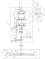
- Fig. 1 shows an active filter 1 for resonance compensation according to a first embodiment in which the active filter 1 is in connection with an electrical system 2.
- the electrical system 2 comprises an AC power source 20 distributing an alternating current to an Alternate Current (AC) conductor 21 for transfer to a power consuming unit 22.
- the power source 20 could be a generator producing the alternating current or a transformer used to transform the voltage level from a high voltage power grid level to consumption level.
- the power consuming unit 22 is for example an electrical machine transforming the electrical energy supplied from the power source 20 via the AC conductor 21 to mechanical work.
- the active filter 1 comprises a Direct Current (DC) power source 10 connected to a switch 11 (or switching unit/system) in a control unit 16.
- the switch 11 creates a compensating current by means of Pulse Width Modulation (PWM) such that the average value of the current fed to the electrical system 2 is controlled by the switch 11 being open and closed at a fast pace. The longer the switch 11 is closed compared to the open periods, the larger the current supplied to the electrical system 2 becomes.
- PWM Pulse Width Modulation
- the switch 11 is connected to an inductor 12.
- U Ldl/dt.
- the inductor typically is an inductor in the range 200-250 uH.
- the inductor 12 is in turn connected to the conductor 3 connecting the active filter 1 to the electrical system 2, such that the current created by the active filter 1 can be supplied to the electrical system 2.
- An additional conductor 15′′′ connects the conductor 3 to a capacitor 13 which in turn is connected to ground 14.
- the measured signal is transferred from the measurement unit 17' to a computing unit 17" adapted to compute a compensating current for reducing frequency components of the current other than the utility frequency, further details with relation to the computation/creation of the compensating current will be described with reference to figs. 3-4 .
- the computing unit 17" is connected to a switching unit (or system) 17′′′, and the compensating current is realized by means of PWM by the switch 11 of the switching unit 17′′′, i.e. the compensating current is supplied from the DC source 10 and formed using PWM by the switching unit 17'".
- the active filter 1 comprises a direct current power source 10, here comprising a capacitor 37 in parallel with a resistor 38.
- the DC power source 10 is connected to a switching unit 17′′′ via conductors 32'; 32".
- the switching unit comprises transistor bridges 31a; 31b; 31c of pair-wise switches (one of which is enlarged and indicated by reference numeral 31a") one top for supplying positive voltages and one bottom for supplying negative voltages for each of the three phases.
- Each switch, such as 31a" comprises a transistor 36, a diode 35 and a snubber 34, connected in parallel with the collector 36" and emitter 36′′′ of the transistor.
- the gate 36' of the transistors 36 are connected to control leads 33a; 33b; 33c running from the computing unit 17" such that the switches operate on pulses from the computing unit 17" affecting the semiconducting properties of the transistor 36.
- the transistors are Insulated Gate Bipolar Transistors (IGBT) which are highly efficient and offers fast switching, however it is conceivable that the transistors are of a different type, such as Metal Oxide Semiconductor Field Effect Transistors (MOSFET).
- the inductors 12a; 12b; 12c and capacitances 13a; 13b; 13c are furthermore adjusted such that the filter short-circuits harmonics and disturbances which are generated by the switching of the transistor bridges 31a; 31b; 31c are reduced/attenuated.
- the control unit 16 of the active filter 1 encompasses a measuring unit 17' connected via measurement conductors 18a; 18b; 18c to a point at the conductors 3a; 3b; 3c between the AC power source 20 and the capacitors 13a; 13b; 13c such that the voltage level of the components of the alternating current with frequencies above the utility frequency, passing through the conductor 13a; 13b; 13c will be measured with high accuracy and low latency.
- the measurement unit 17' is connected to a computing unit 17" in which the Pulse Width Modulation (PWM) creating the control pulses to the switches is computed.
- the computing unit 17" comprises a processing unit, which may be a single CPU (Central processing unit), or could comprise two or more processing units.
- the processor may include a general purpose microprocessor, an instruction set processor and/or related chips sets and/or special purpose microprocessors such as ASICs (Application Specific Integrated Circuit).
- the processor may also comprise board memory for caching purposes.
- the switch system 17′′′ is connected to inductors 12a; 12b; 12c which transform the pulses generated by the switch system 17′′′ to a continuous signal by opposing the changes in current through it by developing a voltage across it proportional to the rate of change of the current.
- the inductors 12a; 12b; 12c are in turn connected to conductors 3a; 3b; 3c connecting the active filter 1 to the electrical system 2, such that the current created by the active filter 1 can be supplied to the electrical system 2.
- the measured signal is transferred from the measurement unit 17' to a computing unit 17" adapted to compute a compensating current for suppressing resonance and reducing frequency components of the current other than the utility frequency. Further details with relation to the computation/creation of the compensating current will be described with reference to fig. 3-4 .
- the computing unit 17" is connected to a switching system (or unit) 17′′′ that realizes the compensating current by means of PWM.
- the compensating current (or currents) will be created by means of one or more digital biquadratic filters.
- the DC power source does not generate any current of its own; it merely stores energy which it takes from the AC phases short periods of time such that the DC current should flow continuously.
- the switches in the switching system (further described under reference to fig. 2 ) needs to be set such that power is received from one AC phase and then distributed to another AC phase in accordance with a switching schedule which will be describes later.
- Fig. 3b shows the actual utility frequency of AC1 when modulated in relation to the perfect sinusoidal reference signal AREF.
- the modulation operates by sending a compensating current out to the grid and thereby switching the direction of the error vector which keeps the error within the thresholds T1 and T2.
- the error vector should be kept within the first threshold T1 and the switching should be adapted such that each switch cycle is as long as possible, which keeps down the power consumption of the switches and prolongs the life of the switches.
- Fig. 4a also shows the actual current I out delivered by the active filter (via the switching system 17′′′) to the electric system 2.
- the difference between the reference current I setp and the delivered current I out is shown as an error I err which is to be kept within a hexagon 64 of thresholds.
- Fig. 4c shows the inner 64 and outer 65 hexagon having an inner and outer threshold for the three phases (AC1, AC2, AC3) respectively.
- the thresholds can be controlled by a digital potentiometer and tuned depending on the system in which the active filter is placed, such that the response from the filter most efficiently suppresses the errors and whilst consuming as little energy as possible.
- the reference current I setp in fig 4b may be based on both a measured current and a measured voltage. Biquadratic filters are applied to these measured signals (independently) and the reference current I setp may e.g. be formed as a sum of these contributions.
- Table 1 SI SII SIII SIV SV SVI 4 Z 5 Z 6 Z 4 Z 2 Z 3 Z
- a current error threshold (85) is set in the control logic of the active filter for defining to what extent a current error can be accepted and defining what the response to the current error should be.
- the method then comprises the step of creating a first current flow (86) between a DC power source and the electrical system based on the current error vector using a first switching pattern, when the current error vector is below the threshold (which is further explained under reference to figs. 4c , 5a and 5b ).
- the method further comprises the step of creating a second (87), different, current flow between the DC power source and the electrical system based on the current error vector using a second switching pattern, when the derived current is above the threshold.
Landscapes
- Engineering & Computer Science (AREA)
- Power Engineering (AREA)
- Inverter Devices (AREA)
- Supply And Distribution Of Alternating Current (AREA)
- Electrotherapy Devices (AREA)
Description
- The invention relates generally to a method and arrangement for reducing resonance using active filters.
- An electrical system or power grid comprises energy generating units and energy consuming units or loads. The energy generating units (or in some instances energy transforming units) in an Alternating Current (AC) system typically generates three alternating currents each having a frequency of 50 or 60 Hz and having an offset relative to each other of 120°. To create a highly effective electrical system, the loads in the system should be purely resistive such that voltage and current waveforms are in phase and changing polarity at the same instance in each cycle. With purely resistive impedance all energy generated in the energy generating units will be turned into a useful and desired energy form at the load. However, in most cases, the impedance contains an inductive or capacitive component, which means that the current consumed is not always in phase with the supplied voltage of the alternating currents. The inductive or capacitive components stores energy temporarily in electric or magnetic fields which is then returned to the power grid a fraction of a second later in the cycle. This process results in a time difference between the current and voltage waveforms creating nonproductive power which increases the current. Furthermore, many electrical apparatus comprises active components that have a dynamically varying load, i.e. the load varies with time, such as electrical apparatus converting electrical power to mechanical work.
- In a normal AC electric system, the voltage varies sinusoidally at a specific frequency, usually 50 or 60 hertz, known as utility frequency. A linear load, even if it comprises inductive or capacitive components, does not change the shape of the waveform of the current. However, the increased use of pulse controlled apparatuses such as rectifiers, variable frequency drives or arc discharge devices, such as a fluorescent lamps, electric welding machines, or arc furnaces introduces non-linear currents into the power grid. Since currents in these systems are interrupted by a switching action, the current contains frequency components that are multiples of the utility frequency, known as harmonics. As nonlinear currents flow through an electrical system and the distribution-transmission lines, additional voltage distortions are produced due to the impedance of the loads and creates a current waveform which can become quite complex, depending on the type of load and its interaction with other components of the system.
- The harmonics are troublesome in many ways; one example is that electric motors experience hysteresis loss caused by eddy currents set up in the iron core of the motor, which are proportional to the frequency of the current. Since the harmonic frequencies are higher, they produce more core loss in a motor than the utility frequency, which results in increased heating of the motor core, which in turn shortens the life of the motor. Other problems with harmonics include overheating of cables and transformers, damage to sensitive equipment and tripping of circuit breakers.
- Active filters capable of reducing the inductive and/or capacitive components and harmonics are known in the art, for example in
US7245045 to Ström et al. An active filter is in principle a microprocessor controlled amplifier which is connected to the power grid, and which is arranged to sense and compensate the load's current consumption with regards to frequencies which would not exist if the load was purely resistive. - Typically, an active filter comprises a main circuit with one or a series of fast switches for each phase and each switch is connected to a power source, such as a Direct Current (DC) power source which can accumulate electrical energy. The power grid's current provision and the load's current consumption are measured, and using Pulse Width Modulation (PWM) a compensating current is distributed to the power system by means of the switches.
- The current flowing in the electrical system is measured by means of a current measurement unit, after which it is transferred to a computing unit that typically transforms the measured current into a digital frequency domain signal using Fast Fourier Transformation (FFT). The transformed signal is used to create an inverted digital signal which is distributed to the electrical system as a compensating current by means of Pulse Width Modulation (PWM).
- The active filters of the art comprise a filter circuit arranged in order to reduce disturbances on the power grid generated by the active filter. Since the active filter in principle is an amplifier, and since the filter circuit comprises an inductor and a capacitor it may form a resonant circuit together with the electrical system which amplifies harmonic frequencies when resonance occurs. Resonance of the power grid may be detrimental by causing unwanted sustained and transient oscillations, which in turn may cause performance degradation. The power grid resonance at the resonant frequency may introduce substantial voltage fluctuation. The effects of resonance in an electrical system may be progressively worsening as higher frequencies are generated. Especially critical for creating resonant behavior is harmonics of 7:th and 11:th order.
- Active filters in the art measures the current flowing between the AC power source and a power consuming device. Since the current flowing in the conductors of the electrical system is a result of the voltage in the power source and impedance of the consuming device, in accordance with Ohm's law I = U/R, the measurement of the current will be delayed in relation to fluctuations of the voltage level. On top of that, active filters use an A/D conversion based on Fast Fourier Transform (FFT) which requires relatively computing intense calculations in the microprocessor before a compensating current can be generated. Since the process of creating a compensating current is much too slow for handling resonance, the response of active filters in the art to resonant behavior in the electrical system has been to shut down the filter and deal with the frequencies generating the resonance by adding components to the electrical system.
- JPH11-178214 is another prior art document providing an active filter device which can stably and economically suppress higher harmonics generated from a load, without being effected by the electric currents of power capacitor facilities by using a resonance frequency band rejecting filter of an active filter control circuit. The filter cuts off the electric currents of power capacitor facilities by reducing the currents near the series resonance frequency of the facilities. The occurrence of harmonic currents is suppressed by only injecting the current of the load, from which the capacitor current are cut off, as a compensation current.
- It is an object of the embodiments herein to address at least some of the problems and shortcomings outlined above by using a method and a control unit as defined in the attached independent claims.
- Further possible features and benefits of this solution will become apparent from the detailed description below. Please note that any embodiment or part of embodiment as well as any method or part of method could be combined in any way.
- Some possible embodiments will now be described, by way of example, with reference to the accompanying drawings, in which:
-
Fig. 1 is a system overview of an active filter; -
Fig. 2 is a system overview of an active filter for a three-phase system shown in further detail; -
Fig. 3a shows a graph of the three currents with a 120° phase shift; -
Fig. 3b shows a graph of a utility frequency when modulated in relation to a perfect sinusoidal reference signal; -
Fig. 4a shows a graph of a resulting error vector and a hexagon made of thresholds; -
Fig. 4b is a system overview of an active filter; -
Fig. 4c is a graph of the error vector in relation to the hexagon thresholds; -
Fig. 5a is a system overview of an active filter showing the units in further detail; -
Fig. 5b is a graph explaining the switching states; -
Fig. 6 is a flow chart explaining a method of suppressing resonance in an electric system; and -
Fig. 7 is a flow chart explaining a control method for an active filter. - An active filter is provided for reducing resonance in a power system by rapidly responding to resonant behavior and instantaneously providing a compensating current actively suppressing the resonance. The rapid response time is enabled by utilizing voltage measurement on a conductor between the electrical system to be monitored and compensated, and a capacitor adapted to attract alternating currents having frequencies above the utility frequency of the electrical system, and by using a biquadratic filter when computing a compensating current.
- By measuring the voltage at this location an instantaneous value on the voltage level of potentially harmful currents is collected since the measured voltage level instantaneously reflects the voltage level of the power system, in contrast to currents which depend upon a current build up over the impedance in response to a change in voltage.
- The feeding of the compensating current, by means of switches and Pulse Width Modulation (PWM), is controlled based on time-domain signals, such as the measured voltages, and the computing power intense step of creating a Fast Fourier Transform (FFT) of such time domain signals is eliminated. This reduces latency and allows for a more rapid response to resonant behavior by more rapidly providing a compensating current actively suppressing the resonance
- A modulation method based on two thresholds is further provided. The two thresholds enables the system to react in a first, less powerful, way as long as the current error (deviation from the desired utility frequency current) is kept below the first threshold, which optimizes the switching for switching as few times per second is possible, which makes the active filter consume less energy and reduces the strain on the active components, which prolongs the life of the active filter. As the current error passes the first threshold, the filter responds very powerfully by ignoring the amount of switches that needs to be made, instead the compensating current created is substantially the opposite to the current error and thus reduces the current error as efficiently and rapidly as possible, which enables the system to react to resonances in the power grid excited by the load to be compensated.
- In the following a detailed description of embodiments will be given with reference to the accompanying drawings. It will be appreciated that the drawings are for illustration only and are not in any way restricting the scope.
-
Fig. 1 shows anactive filter 1 for resonance compensation according to a first embodiment in which theactive filter 1 is in connection with anelectrical system 2. Theelectrical system 2 comprises anAC power source 20 distributing an alternating current to an Alternate Current (AC) conductor 21 for transfer to apower consuming unit 22. Thepower source 20 could be a generator producing the alternating current or a transformer used to transform the voltage level from a high voltage power grid level to consumption level. Thepower consuming unit 22 is for example an electrical machine transforming the electrical energy supplied from thepower source 20 via the AC conductor 21 to mechanical work. - The
active filter 1 is connected to theelectrical system 2 via aconductor 3 placed between theactive filter circuit 1 and the AC conductor 21, such that electrical current generated by theactive filter 1 can be distributed to theelectrical system 2 for improving the characteristics of the alternating current flowing in the AC conductor 21. - The
active filter 1 comprises a Direct Current (DC)power source 10 connected to a switch 11 (or switching unit/system) in acontrol unit 16. The switch 11 creates a compensating current by means of Pulse Width Modulation (PWM) such that the average value of the current fed to theelectrical system 2 is controlled by the switch 11 being open and closed at a fast pace. The longer the switch 11 is closed compared to the open periods, the larger the current supplied to theelectrical system 2 becomes. - Via a second conductor 15", the switch 11 is connected to an
inductor 12. Theinductor 12 transforms the pulses generated by the switch 11 to a continuous signal by opposing the changes in current through it by developing a voltage across it proportional to the rate of change of the current in accordance with the mathematical formula U = Ldl/dt. For an active filter configured for 100A current the inductor typically is an inductor in the range 200-250 uH. Theinductor 12 is in turn connected to theconductor 3 connecting theactive filter 1 to theelectrical system 2, such that the current created by theactive filter 1 can be supplied to theelectrical system 2. An additional conductor 15‴ connects theconductor 3 to a capacitor 13 which in turn is connected to ground 14. The capacitor 13 is set at a value allowing alternating currents with a frequency at magnitudes above the utility frequency of the electrical current (for power grid applications typically 50 - 60 Hz) to pass to theground 14 connection. This will effectively draw all frequencies that create loss in theelectrical system 2 to the capacitor. - The
control system 16 comprises a measurement unit 17' connected via ameasurement conductor 18 to a point at the conductor 21; 3; 15‴ between theAC power source 20 and the capacitor 13 such that the voltage level of the components of the alternating current with frequencies above the utility frequency, passing through the conductor 21; 3; 15‴, will be measured with high accuracy and low latency. - The measured signal is transferred from the measurement unit 17' to a
computing unit 17" adapted to compute a compensating current for reducing frequency components of the current other than the utility frequency, further details with relation to the computation/creation of the compensating current will be described with reference tofigs. 3-4 . Thecomputing unit 17" is connected to a switching unit (or system) 17‴, and the compensating current is realized by means of PWM by the switch 11 of the switchingunit 17‴, i.e. the compensating current is supplied from theDC source 10 and formed using PWM by the switching unit 17'". -
Fig. 2 shows a version of theelectrical system 2 similar to the electrical system described with reference tofig. 1 . The main difference being that the system according tofig. 2 is a three phase system, such as most power grids, comprising three alternating currents each with a phase offset of 120° and each connected to a threephase load 22, for example by means of a Δ or Y coupling. The electrical system comprises 3conductors 21a; 21b; 21c for transferring electrical current from theAC source 20 to theload 22. - Just like in the circuit described under reference to
fig. 1 , theactive filter 1 comprises a directcurrent power source 10, here comprising acapacitor 37 in parallel with aresistor 38. TheDC power source 10 is connected to aswitching unit 17‴ via conductors 32'; 32". According to the embodiment shown under reference tofig. 2 the switching unit comprisestransistor bridges 31a; 31b; 31c of pair-wise switches (one of which is enlarged and indicated byreference numeral 31a") one top for supplying positive voltages and one bottom for supplying negative voltages for each of the three phases. Each switch, such as 31a", comprises atransistor 36, adiode 35 and asnubber 34, connected in parallel with thecollector 36" andemitter 36‴ of the transistor. Thetransistor 36 is the active component that controls the PWM, thediode 35 directs current from theelectrical system 2 to the DC accumulator when the voltage of theelectrical system 2 exceeds the voltage of the DC accumulator. Thesnubber 34 protects the transistor from short voltage spikes that are created when the switch turns off the current by absorbing and reducing the voltage to manageable levels i.e. 50 - 100V. For each phase, the pair of switches are in one end connected to each other and to the conductors 15"a; 15"b; 15"c, and their other ends connected to theDC power source 10 by means of shared conductors 32'; 32". Both the specific design of theDC power source 10 and the switches are to be seen as examples of implementations. The skilled person realized that variations or alternatives to the designs are equally conceivable. - The gate 36' of the
transistors 36 are connected to controlleads 33a; 33b; 33c running from thecomputing unit 17" such that the switches operate on pulses from thecomputing unit 17" affecting the semiconducting properties of thetransistor 36. In the embodiment described under reference tofig. 2 , the transistors are Insulated Gate Bipolar Transistors (IGBT) which are highly efficient and offers fast switching, however it is conceivable that the transistors are of a different type, such as Metal Oxide Semiconductor Field Effect Transistors (MOSFET). - The
inductors 12a; 12b; 12c andcapacitances 13a; 13b; 13c are furthermore adjusted such that the filter short-circuits harmonics and disturbances which are generated by the switching of thetransistor bridges 31a; 31b; 31c are reduced/attenuated. - The
control unit 16 of theactive filter 1 encompasses a measuring unit 17' connected viameasurement conductors 18a; 18b; 18c to a point at theconductors 3a; 3b; 3c between theAC power source 20 and thecapacitors 13a; 13b; 13c such that the voltage level of the components of the alternating current with frequencies above the utility frequency, passing through theconductor 13a; 13b; 13c will be measured with high accuracy and low latency. The measurement unit 17' is connected to acomputing unit 17" in which the Pulse Width Modulation (PWM) creating the control pulses to the switches is computed. Thecomputing unit 17" comprises a processing unit, which may be a single CPU (Central processing unit), or could comprise two or more processing units. For example, the processor may include a general purpose microprocessor, an instruction set processor and/or related chips sets and/or special purpose microprocessors such as ASICs (Application Specific Integrated Circuit). The processor may also comprise board memory for caching purposes. - As in
fig.1 theswitch system 17‴ is connected toinductors 12a; 12b; 12c which transform the pulses generated by theswitch system 17‴ to a continuous signal by opposing the changes in current through it by developing a voltage across it proportional to the rate of change of the current. Theinductors 12a; 12b; 12c are in turn connected toconductors 3a; 3b; 3c connecting theactive filter 1 to theelectrical system 2, such that the current created by theactive filter 1 can be supplied to theelectrical system 2. - The measured signal is transferred from the measurement unit 17' to a
computing unit 17" adapted to compute a compensating current for suppressing resonance and reducing frequency components of the current other than the utility frequency. Further details with relation to the computation/creation of the compensating current will be described with reference tofig. 3-4 . Thecomputing unit 17" is connected to a switching system (or unit) 17‴ that realizes the compensating current by means of PWM. - Further details of the operation of the computing unit and the creation of the control signal for controlling the switches will now be described under reference to
figs. 3-4 . - The compensating current (or currents) will be created by means of one or more digital biquadratic filters. Biquadratic filters are second-order recursive linear filters having a transfer function which is the ratio of two quadratic functions:

- According to the embodiments described under reference to
figs. 1 and2 the biquadratic filter is digitally implemented in the computing unit (reference number 17") and typically samples the voltage signal with a frequency above 100 kSa/s, preferably above 190kSa/s, which means that sampling is more than 2000, preferably more than 3800, times faster than the utility frequency of the power system (or electric system) which is fast enough to react to resonant behavior of most harmonics in a frequency range that could cause problems. Furthermore, the biquadratic filter has a very low latency which makes the reaction to resonant behavior vary rapid, which enables efficient suppression of the resonant behavior. - According to the embodiments described with reference to
figs. 2 , the DC power source does not generate any current of its own; it merely stores energy which it takes from the AC phases short periods of time such that the DC current should flow continuously. This means that the switches in the switching system (further described under reference tofig. 2 ) needs to be set such that power is received from one AC phase and then distributed to another AC phase in accordance with a switching schedule which will be describes later. - The modulation will now be described in further detail.
-
Fig. 3a shows the utility frequency of the three AC phases AC1, AC2, AC3 in the time/voltage domain. The modulation is hysteresis based such that the difference, or error, between the desired (reference) output current and the actual output current is calculated for the purpose of creating an error vector to be controlled. -
Fig. 3b shows the actual utility frequency of AC1 when modulated in relation to the perfect sinusoidal reference signal AREF. The modulation operates by sending a compensating current out to the grid and thereby switching the direction of the error vector which keeps the error within the thresholds T1 and T2. In normal operations, the error vector should be kept within the first threshold T1 and the switching should be adapted such that each switch cycle is as long as possible, which keeps down the power consumption of the switches and prolongs the life of the switches. -
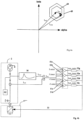
Fig. 4a shows the reference current Isetp obtained by thecontrol unit 16 by applying one or more biquadratic filters to the current in the electric system 2.The current on which the biquadratic filter is applied, may be obtained from the measured voltage. Alternatively, the biquadratic filter may be applied to the measured voltage and the reference current Isetp may then be obtained from the resulting filtered voltage. The reference current Isetp represents resonant components or other undesirable components, in the current in theelectric system 2, which are to be removed or compensated for by the active filter. The biquadratic filters may have been tuned during configuration or setup of the active filter to ensure that resonant components end up in the reference current Isetp while the utility frequency of the electrical system (e.g. 50 or 60 Hz) is attenuated by the biquadratic filters.Fig. 4a also shows the actual current Iout delivered by the active filter (via theswitching system 17‴) to theelectric system 2. The difference between the reference current Isetp and the delivered current Iout is shown as an error Ierr which is to be kept within ahexagon 64 of thresholds. -
Fig. 4b is a simplified system illustration showing thecontrol unit 16 generating the reference current Isetp, which after comparison with the delivered current Iout generates the resulting current error vector Ierr. The resulting current error vector Ierr is then compared with the first and second thresholds in the comparators (51a - 51d). In further detail the error vector Ierr is compared to the second (outer) threshold Iouter in 51a, the first (inner) threshold Iinner in 51b, the first negative (inner) threshold -Iinner in 51c in the second negative (outer) threshold -Iouter in 51d. The comparison results in acontrol signal 33 for controlling the switches such that the most suitable compensating current is created. -
Fig. 4c shows the inner 64 and outer 65 hexagon having an inner and outer threshold for the three phases (AC1, AC2, AC3) respectively. The thresholds can be controlled by a digital potentiometer and tuned depending on the system in which the active filter is placed, such that the response from the filter most efficiently suppresses the errors and whilst consuming as little energy as possible. - In some embodiments, the reference current Isetp in
fig 4b may be based on both a measured current and a measured voltage. Biquadratic filters are applied to these measured signals (independently) and the reference current Isetp may e.g. be formed as a sum of these contributions. -
Fig. 5a shows a circuitry diagram of an embodiment of the modulation system witherror vectors bottom values 52g - I are further provided as input to theouter sector detector 65 adapted to determine whether or not the resulting error vector remains within the boundaries of theouter hexagon 65, which places the resulting error vector Ierr in a sector S - SVI of thehexagon 65 and provides output in the form of the sector SI - SVI to a dynamic-state control unit 67 adapted to control the switch states (of the switches for example shown as 31a - 31c infig. 2 ) in accordance with table 1 below, such that the switching is optimized for effectively pushing the resulting error vector Ierr back into the boundaries of theinner hexagon 64. The switching states of table 1 are realized in accordance with the switching state graph infig. 5b .Table 1 SI SII SIII SIV SV SVI 4 Z 5 Z 6 Z 4 Z 2 Z 3 Z - The required switching states are received at a control
signal generating unit 68 determining if switches need to be made and creates thecontrol signals 33a', 33a", 33b', 33b", 33c', 33c", received as input in the transistor bridges (31a - 31c infig. 2 ) and controlling the transistors such that a compensating current is created by means of pulse width modulation. -
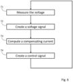
Fig. 6 is a flowchart of a control method for an active filter according to one embodiment. The control method comprises the steps of measuring thevoltage 71 at a point between a capacitor and the electrical system (as further disclosed under reference tofigs. 1 and2 ), creating a voltage signal at acontrol unit 72 representing the voltage of different frequencies in the alternating current, computing 73, at a computing unit, (based on the voltage signal and using a biquadratic filter) a compensating current for suppressing resonant behavior and the voltage level at frequencies other than the utility frequency, and creating acontrol signal 74 on the basis of the voltage signal for controlling switches for generating the compensating current using pulse width modulation (also further disclosed with reference tofigs. 1- 4 ). -
Fig. 7 is a flowchart describing a method of modulation according to one embodiment. The method comprises the steps of measuring a voltage (81) at the electric system for deriving a current (82). The voltage could be measured between a conductor of the electrical system and a capacitor adapted to lead alternating currents with frequencies other that the utility frequency of the electric system to ground, which creates a very good connection between troublesome frequencies and the measurement. The measured voltage is used to derive a current which is then compared (83) with a reference current, having a perfect sinusoidal wave form such that a difference between the reference current and the measured current can be derived (84), the difference being a current error vector. A current error threshold (85) is set in the control logic of the active filter for defining to what extent a current error can be accepted and defining what the response to the current error should be. The method then comprises the step of creating a first current flow (86) between a DC power source and the electrical system based on the current error vector using a first switching pattern, when the current error vector is below the threshold (which is further explained under reference tofigs. 4c ,5a and 5b ). The method further comprises the step of creating a second (87), different, current flow between the DC power source and the electrical system based on the current error vector using a second switching pattern, when the derived current is above the threshold. - Please note that any embodiment or part of embodiment as well as any method or part of method could be combined in any way. All examples herein should be seen as part of the general description and therefore possible to combine in any way in general terms.
Claims (14)
- A control unit (16) for an active filter (1) for reducing resonance in an electric system (2), the electric system (2) comprising a power source (20) distributing a first alternating current (AC1) to a first AC conductor (21a, 21) connected to a power consuming unit (22) for distributing the AC to the power consuming unit, the active filter (1) comprising a DC power source (10) and a conductor (15"; 3) connecting the DC power source (10) to the first AC conductor (21a, 21), the control unit (16) comprising:a voltage measurement unit (17') adapted to create a voltage signal on the basis of a measured voltage of the electric system;a computing unit (17") adapted to compute, using a biquadratic filter, a first compensating current on the basis of the voltage signal for reducing resonance in the electric system (2); anda switching system (17‴) connectable between the DC power source (10) and the conductor (15"; 3) for creating the calculated first compensating current.
- The control unit according to claim 1, wherein the active filter further comprises a capacitor (13) connected to the conductor (15"; 3) and to ground (14) and being adapted to lead frequencies other than a utility frequency of the electrical system to ground (14), and wherein the voltage measurement unit is adapted to be connected to a point between the AC power source (20) and the capacitor (13).
- The control unit according to any one of claims 1 and 2, wherein the computing unit is adapted to apply the biquadratic filter to the voltage signal or to a signal derived based on the voltage signal.
- The control unit according to any one of the preceding claims, wherein the biquadratic filter has a sample frequency exceeding 100kSa/s.
- The control unit according to any one of the preceding claims, wherein the voltage measurement unit (17') is further adapted to measure a second voltage of a second AC conductor (21b) distributing a second alternating current (AC2) and a third voltage of a third AC conductor (21c) distributing a third alternating current (AC3) having an offset in relation to the first alternating current (AC1) of substantially 120° and 240° respectively, and create a second and third voltage signal on the basis of the second and third measured voltages, and wherein the computing unit (17") is further adapted to compute a second and third compensating current on the basis of the second and third voltage signals.
- The control unit according to claim 5, wherein the DC power source (10) is adapted to receive current from the second (AC2) or third (AC3) alternating currents, and wherein the switching system (17‴) is adapted to distribute the first compensating current to the first AC conductor (21a) by means of pulse width modulation.
- The control unit according to any one of the preceding claims, wherein the computing unit is adapted to compute the first compensating current on the basis of the voltage signal and a current signal based on a current measured at the first AC conductor (21a, 21).
- An active filter (1) for reducing resonance in an electric system (2), the electric system comprising a power source (20) distributing a first alternating current (AC1) to a first AC conductor (21a, 21) connected to a power consuming unit (22) for distributing the first alternating current (AC1) to the power consuming unit (22), the active filter (1) comprising:a DC power source (10);a conductor (15"; 3) connecting the DC power source (10) to the first AC conductor (21a, 21); andthe control unit (16) according to any one of claims 1 - 7.
- A method of suppressing resonance in an electric system comprising an active filter, the method comprising:measuring (71) a voltage of a conductor (21) supplying energy from an AC source (20) to an energy consuming unit (22),creating (72) a voltage signal on the basis of the measured voltage,computing (73), using a biquadratic filter, a compensating current on the basis of the voltage signal, andcreating (74) a control signal for controlling a switching system creating the compensating current by means of pulse width modulation.
- The method according to claim 9, wherein the voltage is measured between the conductor (21) and a capacitor (13) adapted to lead alternating currents with frequencies other that the utility frequency of the electric system to ground (14).
- The method according to any one of claims 9 - 10, wherein the step of computing a compensating current on the basis of the voltage signal comprises applying the biquadratic filter to the voltage signal or to a signal derived based on the voltage signal.
- The method according to any one of claims 9 - 11, wherein the step of computing a compensating current on the basis of the voltage signal is performed using a biquadratic filter with a sample frequency of more than 100kSa/s.
- The method according to claim 12, wherein the step of computing a compensating current on the basis of the voltage signal is performed using a biquadratic filter with a sample frequency of more than 150kSa/s.
- The method according to any one of claims 9 - 13, wherein the compensating current is computed on the basis of the voltage signal and a current signal based on a current measured at the conductor.
Applications Claiming Priority (3)
| Application Number | Priority Date | Filing Date | Title |
|---|---|---|---|
| SE1151123A SE536142C2 (en) | 2011-11-25 | 2011-11-25 | Active filter for resonance reduction |
| US201161565785P | 2011-12-01 | 2011-12-01 | |
| PCT/SE2012/051290 WO2013077801A1 (en) | 2011-11-25 | 2012-11-22 | Active filter for resonance reduction |
Publications (4)
| Publication Number | Publication Date |
|---|---|
| EP2783446A1 EP2783446A1 (en) | 2014-10-01 |
| EP2783446A4 EP2783446A4 (en) | 2015-07-29 |
| EP2783446B1 true EP2783446B1 (en) | 2023-12-13 |
| EP2783446C0 EP2783446C0 (en) | 2023-12-13 |
Family
ID=48464165
Family Applications (1)
| Application Number | Title | Priority Date | Filing Date |
|---|---|---|---|
| EP12851560.8A Active EP2783446B1 (en) | 2011-11-25 | 2012-11-22 | Control unit for active filter, active filter and method for resonance reduction |
Country Status (7)
| Country | Link |
|---|---|
| US (3) | US10141741B2 (en) |
| EP (1) | EP2783446B1 (en) |
| CN (2) | CN108718092B (en) |
| ES (1) | ES2972474T3 (en) |
| PL (1) | PL2783446T3 (en) |
| SE (1) | SE536142C2 (en) |
| WO (1) | WO2013077801A1 (en) |
Families Citing this family (15)
| Publication number | Priority date | Publication date | Assignee | Title |
|---|---|---|---|---|
| SE536142C2 (en) * | 2011-11-25 | 2013-05-28 | Comsys Ab | Active filter for resonance reduction |
| US20140376283A1 (en) * | 2013-06-21 | 2014-12-25 | Hamilton Sundstrand Corporation | Systems and methods for active damping device for stabilizing a power grid of active sources and loads |
| US20180287370A1 (en) * | 2013-09-26 | 2018-10-04 | James J. Kinsella | Low-cost, full-range electronc overload relay device |
| US10483758B2 (en) * | 2014-01-08 | 2019-11-19 | Abb Research Ltd. | Method and apparatus for controlling a hybrid energy storage system |
| TWI542114B (en) * | 2015-06-17 | 2016-07-11 | 台達電子工業股份有限公司 | Photovoltaic inverter grid-connected system and method for implementing three-phase ac grid-connected transition |
| EP3118961B1 (en) | 2015-07-17 | 2019-06-05 | "Condensator Dominit" Dr. Christian Dresel Gesellschaft für Leistungselektronik, Energietechnik und Netzqualität mbH | Use of electrical network distortion energy using rectifier |
| GB201601472D0 (en) * | 2016-01-26 | 2016-03-09 | Alstom Grid Uk Ltd | Oscillations in electrical power networks |
| CN110024251B (en) * | 2016-11-15 | 2023-09-08 | 伊莱克斯家用电器股份公司 | Monitoring arrangement for household or commercial appliances |
| JP2018196264A (en) * | 2017-05-18 | 2018-12-06 | アイシン精機株式会社 | Noise removal circuit |
| CN111130113A (en) * | 2020-01-07 | 2020-05-08 | 河北工程大学 | Method and system for determining compensation current of active power filter |
| CN113839388B (en) * | 2021-11-29 | 2022-02-08 | 湖北工业大学 | Current double-loop control method of active power filter based on hybrid load |
| CN114749359B (en) * | 2022-06-14 | 2022-09-06 | 深圳市汇顶科技股份有限公司 | Signal generating circuit and ultrasonic fingerprint identification device |
| EP4557246A4 (en) | 2022-07-14 | 2025-08-27 | Huike Singapore Holding Pte Ltd | ULTRASONIC FINGERPRINT DETECTION DEVICE AND ELECTRONIC EQUIPMENT |
| CN115275962B (en) * | 2022-07-14 | 2025-05-09 | 浙江大学 | A method and device for stabilizing DC side voltage of inverter |
| CN115347842B (en) * | 2022-10-12 | 2023-01-24 | 旋智电子科技(上海)有限公司 | Permanent magnet synchronous motor current control method based on constrained model predictive control |
Family Cites Families (22)
| Publication number | Priority date | Publication date | Assignee | Title |
|---|---|---|---|---|
| US4067766A (en) | 1976-02-23 | 1978-01-10 | Larger George K | Automatic building block laying panel-forming machine and method |
| DE2813946C2 (en) | 1978-03-31 | 1980-01-31 | Siemens Ag, 1000 Berlin Und 8000 Muenchen | Filter circuit with a biquadratic transfer function |
| JPH02262840A (en) | 1989-04-03 | 1990-10-25 | Toshiba Corp | Controller for active filter |
| JP2728575B2 (en) * | 1991-06-14 | 1998-03-18 | 株式会社日立製作所 | Power conversion method and device |
| JPH11178214A (en) * | 1997-12-04 | 1999-07-02 | Toshiba Corp | Active filter device |
| US6038152A (en) * | 1998-12-03 | 2000-03-14 | Baker; Donal E. | Active rectifier utilizing a fixed switching pattern |
| JP3661012B2 (en) | 2001-04-20 | 2005-06-15 | 国立大学法人 岡山大学 | Power distribution system active filter device and control system |
| TWI243526B (en) * | 2004-08-11 | 2005-11-11 | Uis Abler Electronics Co Ltd | Three-phase three-wire active power filter |
| TWI236792B (en) * | 2004-08-30 | 2005-07-21 | Uis Abler Electronics Co Ltd | Active equipment for harmonic suppression |
| CN100340043C (en) * | 2004-08-31 | 2007-09-26 | 浙江大学 | Series active power filter |
| CN100346550C (en) * | 2005-07-18 | 2007-10-31 | 西安交通大学 | Control method for restraining oscillate based on mixed electric power filter |
| US7391181B2 (en) | 2006-03-16 | 2008-06-24 | General Motors Corporation | Loss minimized PWM for voltage source inverters taking into account inverter non-linearity |
| TWI347058B (en) * | 2007-03-05 | 2011-08-11 | Ablerex Electronics Co Ltd | Active power filter apparatus |
| CN201075697Y (en) * | 2007-04-23 | 2008-06-18 | 电鳐科技(北京)有限公司 | Active filtering electric power electricity saver |
| US8232784B2 (en) * | 2008-04-01 | 2012-07-31 | O2Micro, Inc | Circuits and methods for current sensing |
| CN101478161B (en) | 2009-01-21 | 2011-05-25 | 中南大学 | A Compensation Current Control Method for Active Power Filter under Non-ideal Voltage Condition |
| CN201417950Y (en) * | 2009-05-22 | 2010-03-03 | 山东鲁电电气集团有限公司 | Active filtering device |
| CN101630842A (en) * | 2009-08-12 | 2010-01-20 | 江苏大学 | Implementation method of inverse system controller of active power filter |
| EP2556575B1 (en) | 2010-04-06 | 2015-03-18 | Danfoss Drives A/S | Power quality improvement by active filter |
| CN201699418U (en) * | 2010-04-22 | 2011-01-05 | 武汉市通益电气有限公司 | Novel parallelly-connected active filter |
| US20110264299A1 (en) * | 2010-04-27 | 2011-10-27 | Siemens Industry, Inc. | Method and system for managing power quality and efficiency |
| SE536142C2 (en) * | 2011-11-25 | 2013-05-28 | Comsys Ab | Active filter for resonance reduction |
-
2011
- 2011-11-25 SE SE1151123A patent/SE536142C2/en not_active IP Right Cessation
-
2012
- 2012-11-22 PL PL12851560.8T patent/PL2783446T3/en unknown
- 2012-11-22 CN CN201810708752.1A patent/CN108718092B/en active Active
- 2012-11-22 EP EP12851560.8A patent/EP2783446B1/en active Active
- 2012-11-22 WO PCT/SE2012/051290 patent/WO2013077801A1/en not_active Ceased
- 2012-11-22 ES ES12851560T patent/ES2972474T3/en active Active
- 2012-11-22 CN CN201280057812.9A patent/CN104145393B/en active Active
- 2012-11-22 US US14/360,700 patent/US10141741B2/en active Active
-
2018
- 2018-10-25 US US16/170,708 patent/US10944264B2/en active Active
-
2021
- 2021-02-02 US US17/164,999 patent/US11349307B2/en active Active
Also Published As
| Publication number | Publication date |
|---|---|
| US20210159697A1 (en) | 2021-05-27 |
| SE1151123A1 (en) | 2013-05-26 |
| US20150102689A1 (en) | 2015-04-16 |
| WO2013077801A1 (en) | 2013-05-30 |
| EP2783446C0 (en) | 2023-12-13 |
| US11349307B2 (en) | 2022-05-31 |
| PL2783446T3 (en) | 2024-09-16 |
| CN108718092A (en) | 2018-10-30 |
| US10944264B2 (en) | 2021-03-09 |
| US20190131790A1 (en) | 2019-05-02 |
| SE536142C2 (en) | 2013-05-28 |
| ES2972474T3 (en) | 2024-06-12 |
| CN104145393B (en) | 2018-07-24 |
| US10141741B2 (en) | 2018-11-27 |
| CN108718092B (en) | 2022-08-19 |
| EP2783446A4 (en) | 2015-07-29 |
| EP2783446A1 (en) | 2014-10-01 |
| CN104145393A (en) | 2014-11-12 |
Similar Documents
| Publication | Publication Date | Title |
|---|---|---|
| US11349307B2 (en) | Active filter for resonance reduction | |
| Mallik et al. | Control of a three-phase boost PFC converter using a single DC-link voltage sensor | |
| CA2838384C (en) | Paralleling of active filters with independent controls | |
| Moran et al. | A series active power filter which compensates current harmonics and voltage unbalance simultaneously | |
| US20150207398A1 (en) | Power conversion system having a harmonic distortion limiter | |
| Jacob et al. | A review of active power filters in power system applications | |
| Lidozzi et al. | Sinusoidal voltage shaping of inverter-equipped stand-alone generating units | |
| US11967891B2 (en) | Mitigation of harmonic disturbances in a power converter | |
| Yi et al. | Comparison analysis of resonant controllers for current regulation of selective active power filter with mixed current reference | |
| Mukherjee et al. | Power System Harmonic Reduction using Shunt Active Filter | |
| López-Robles et al. | Voltage regulation of a matrix converter with balanced and unbalanced three-phase loads | |
| Li et al. | Comparison of current control techniques for single-phase voltage-source PWM rectifiers | |
| Lei et al. | Evaluation and improvement of active stabilization method for matrix converter under input voltage disturbances | |
| Upadhyay et al. | Shunt active power filter (SAPF) design and analysis of harmonics mitigation in three-phase three-wire distribution system | |
| Longhui et al. | Stability analysis and controller design of hybrid compensation system with parallel active power filter and parallel capacitors | |
| Mukherjee et al. | Power system harmonic compensation using shunt active power filter | |
| RU2524347C2 (en) | Device for earth fault current compensation in three-phase electrical networks (versions) | |
| Zhu et al. | Dual-loop pr control for collapsed h-bridge single-phase 400hz power supply | |
| Rymarski et al. | The dynamic properties of a single‐phase transformer‐based inverter for ups systems | |
| Szromba | Three-phase four-wire shunt active power filter working simultaneously as energy conditioner | |
| Jacobina et al. | Three-phase series active power filter without dc voltage source | |
| Aware et al. | Power factor improvement using active filter for unbalanced three-phase non-linear loads | |
| CN108233374B (en) | A method and system for suppressing impact load harmonics of prefabricated box-type transformers | |
| Chaudhari et al. | Three-Level Shunt Active Filter for Power Quality Improvement | |
| Mohammed | Analysis and Simulation of Shunt Active Power Filter For Harmonic Cancellation of Non Linear Loads |
Legal Events
| Date | Code | Title | Description |
|---|---|---|---|
| PUAI | Public reference made under article 153(3) epc to a published international application that has entered the european phase |
Free format text: ORIGINAL CODE: 0009012 |
|
| 17P | Request for examination filed |
Effective date: 20140521 |
|
| AK | Designated contracting states |
Kind code of ref document: A1 Designated state(s): AL AT BE BG CH CY CZ DE DK EE ES FI FR GB GR HR HU IE IS IT LI LT LU LV MC MK MT NL NO PL PT RO RS SE SI SK SM TR |
|
| RIN1 | Information on inventor provided before grant (corrected) |
Inventor name: PERSSON, JONAS |
|
| DAX | Request for extension of the european patent (deleted) | ||
| RA4 | Supplementary search report drawn up and despatched (corrected) |
Effective date: 20150630 |
|
| RIC1 | Information provided on ipc code assigned before grant |
Ipc: H02J 3/01 20060101ALI20150622BHEP Ipc: H02J 3/18 20060101AFI20150622BHEP |
|
| STAA | Information on the status of an ep patent application or granted ep patent |
Free format text: STATUS: EXAMINATION IS IN PROGRESS |
|
| 17Q | First examination report despatched |
Effective date: 20210211 |
|
| REG | Reference to a national code |
Ref country code: DE Ref legal event code: R079 Free format text: PREVIOUS MAIN CLASS: H02J0003180000 Ipc: H02J0003010000 Ref document number: 602012080408 Country of ref document: DE |
|
| RIC1 | Information provided on ipc code assigned before grant |
Ipc: H02J 3/24 20060101ALI20230620BHEP Ipc: H02J 3/18 20060101ALI20230620BHEP Ipc: H02J 3/01 20060101AFI20230620BHEP |
|
| GRAP | Despatch of communication of intention to grant a patent |
Free format text: ORIGINAL CODE: EPIDOSNIGR1 |
|
| STAA | Information on the status of an ep patent application or granted ep patent |
Free format text: STATUS: GRANT OF PATENT IS INTENDED |
|
| INTG | Intention to grant announced |
Effective date: 20230731 |
|
| GRAS | Grant fee paid |
Free format text: ORIGINAL CODE: EPIDOSNIGR3 |
|
| GRAA | (expected) grant |
Free format text: ORIGINAL CODE: 0009210 |
|
| STAA | Information on the status of an ep patent application or granted ep patent |
Free format text: STATUS: THE PATENT HAS BEEN GRANTED |
|
| AK | Designated contracting states |
Kind code of ref document: B1 Designated state(s): AL AT BE BG CH CY CZ DE DK EE ES FI FR GB GR HR HU IE IS IT LI LT LU LV MC MK MT NL NO PL PT RO RS SE SI SK SM TR |
|
| REG | Reference to a national code |
Ref country code: GB Ref legal event code: FG4D |
|
| REG | Reference to a national code |
Ref country code: CH Ref legal event code: EP |
|
| REG | Reference to a national code |
Ref country code: DE Ref legal event code: R096 Ref document number: 602012080408 Country of ref document: DE |
|
| REG | Reference to a national code |
Ref country code: IE Ref legal event code: FG4D |
|
| U01 | Request for unitary effect filed |
Effective date: 20231213 |
|
| U07 | Unitary effect registered |
Designated state(s): AT BE BG DE DK EE FI FR IT LT LU LV MT NL PT SE SI Effective date: 20231218 |
|
| RAP4 | Party data changed (patent owner data changed or rights of a patent transferred) |
Owner name: COMSYS AB |
|
| U1H | Name or address of the proprietor changed after the registration of the unitary effect |
Owner name: COMSYS AB; SE |
|
| REG | Reference to a national code |
Ref country code: NO Ref legal event code: T2 Effective date: 20231213 |
|
| PG25 | Lapsed in a contracting state [announced via postgrant information from national office to epo] |
Ref country code: GR Free format text: LAPSE BECAUSE OF FAILURE TO SUBMIT A TRANSLATION OF THE DESCRIPTION OR TO PAY THE FEE WITHIN THE PRESCRIBED TIME-LIMIT Effective date: 20240314 |
|
| PG25 | Lapsed in a contracting state [announced via postgrant information from national office to epo] |
Ref country code: GR Free format text: LAPSE BECAUSE OF FAILURE TO SUBMIT A TRANSLATION OF THE DESCRIPTION OR TO PAY THE FEE WITHIN THE PRESCRIBED TIME-LIMIT Effective date: 20240314 |
|
| PG25 | Lapsed in a contracting state [announced via postgrant information from national office to epo] |
Ref country code: RS Free format text: LAPSE BECAUSE OF FAILURE TO SUBMIT A TRANSLATION OF THE DESCRIPTION OR TO PAY THE FEE WITHIN THE PRESCRIBED TIME-LIMIT Effective date: 20231213 Ref country code: HR Free format text: LAPSE BECAUSE OF FAILURE TO SUBMIT A TRANSLATION OF THE DESCRIPTION OR TO PAY THE FEE WITHIN THE PRESCRIBED TIME-LIMIT Effective date: 20231213 |
|
| REG | Reference to a national code |
Ref country code: ES Ref legal event code: FG2A Ref document number: 2972474 Country of ref document: ES Kind code of ref document: T3 Effective date: 20240612 |
|
| PG25 | Lapsed in a contracting state [announced via postgrant information from national office to epo] |
Ref country code: IS Free format text: LAPSE BECAUSE OF FAILURE TO SUBMIT A TRANSLATION OF THE DESCRIPTION OR TO PAY THE FEE WITHIN THE PRESCRIBED TIME-LIMIT Effective date: 20240413 |
|
| PG25 | Lapsed in a contracting state [announced via postgrant information from national office to epo] |
Ref country code: CZ Free format text: LAPSE BECAUSE OF FAILURE TO SUBMIT A TRANSLATION OF THE DESCRIPTION OR TO PAY THE FEE WITHIN THE PRESCRIBED TIME-LIMIT Effective date: 20231213 |
|
| PG25 | Lapsed in a contracting state [announced via postgrant information from national office to epo] |
Ref country code: SK Free format text: LAPSE BECAUSE OF FAILURE TO SUBMIT A TRANSLATION OF THE DESCRIPTION OR TO PAY THE FEE WITHIN THE PRESCRIBED TIME-LIMIT Effective date: 20231213 |
|
| PG25 | Lapsed in a contracting state [announced via postgrant information from national office to epo] |
Ref country code: SM Free format text: LAPSE BECAUSE OF FAILURE TO SUBMIT A TRANSLATION OF THE DESCRIPTION OR TO PAY THE FEE WITHIN THE PRESCRIBED TIME-LIMIT Effective date: 20231213 Ref country code: SK Free format text: LAPSE BECAUSE OF FAILURE TO SUBMIT A TRANSLATION OF THE DESCRIPTION OR TO PAY THE FEE WITHIN THE PRESCRIBED TIME-LIMIT Effective date: 20231213 Ref country code: RO Free format text: LAPSE BECAUSE OF FAILURE TO SUBMIT A TRANSLATION OF THE DESCRIPTION OR TO PAY THE FEE WITHIN THE PRESCRIBED TIME-LIMIT Effective date: 20231213 Ref country code: IS Free format text: LAPSE BECAUSE OF FAILURE TO SUBMIT A TRANSLATION OF THE DESCRIPTION OR TO PAY THE FEE WITHIN THE PRESCRIBED TIME-LIMIT Effective date: 20240413 Ref country code: CZ Free format text: LAPSE BECAUSE OF FAILURE TO SUBMIT A TRANSLATION OF THE DESCRIPTION OR TO PAY THE FEE WITHIN THE PRESCRIBED TIME-LIMIT Effective date: 20231213 |
|
| REG | Reference to a national code |
Ref country code: DE Ref legal event code: R097 Ref document number: 602012080408 Country of ref document: DE |
|
| PLBE | No opposition filed within time limit |
Free format text: ORIGINAL CODE: 0009261 |
|
| STAA | Information on the status of an ep patent application or granted ep patent |
Free format text: STATUS: NO OPPOSITION FILED WITHIN TIME LIMIT |
|
| 26N | No opposition filed |
Effective date: 20240916 |
|
| U20 | Renewal fee for the european patent with unitary effect paid |
Year of fee payment: 13 Effective date: 20241016 |
|
| PG25 | Lapsed in a contracting state [announced via postgrant information from national office to epo] |
Ref country code: MC Free format text: LAPSE BECAUSE OF FAILURE TO SUBMIT A TRANSLATION OF THE DESCRIPTION OR TO PAY THE FEE WITHIN THE PRESCRIBED TIME-LIMIT Effective date: 20231213 |
|
| PG25 | Lapsed in a contracting state [announced via postgrant information from national office to epo] |
Ref country code: IE Free format text: LAPSE BECAUSE OF NON-PAYMENT OF DUE FEES Effective date: 20241122 |
|
| U20 | Renewal fee for the european patent with unitary effect paid |
Year of fee payment: 14 Effective date: 20251016 |
|
| REG | Reference to a national code |
Ref country code: CH Ref legal event code: U11 Free format text: ST27 STATUS EVENT CODE: U-0-0-U10-U11 (AS PROVIDED BY THE NATIONAL OFFICE) Effective date: 20251201 |
|
| PGFP | Annual fee paid to national office [announced via postgrant information from national office to epo] |
Ref country code: GB Payment date: 20251016 Year of fee payment: 14 |
|
| PGFP | Annual fee paid to national office [announced via postgrant information from national office to epo] |
Ref country code: NO Payment date: 20251021 Year of fee payment: 14 |
|
| PGFP | Annual fee paid to national office [announced via postgrant information from national office to epo] |
Ref country code: CH Payment date: 20251201 Year of fee payment: 14 |
|
| PGFP | Annual fee paid to national office [announced via postgrant information from national office to epo] |
Ref country code: PL Payment date: 20251013 Year of fee payment: 14 |
|
| PGFP | Annual fee paid to national office [announced via postgrant information from national office to epo] |
Ref country code: ES Payment date: 20251201 Year of fee payment: 14 |
|
| PG25 | Lapsed in a contracting state [announced via postgrant information from national office to epo] |
Ref country code: HU Free format text: LAPSE BECAUSE OF FAILURE TO SUBMIT A TRANSLATION OF THE DESCRIPTION OR TO PAY THE FEE WITHIN THE PRESCRIBED TIME-LIMIT; INVALID AB INITIO Effective date: 20121122 |
|
| PG25 | Lapsed in a contracting state [announced via postgrant information from national office to epo] |
Ref country code: CY Free format text: LAPSE BECAUSE OF FAILURE TO SUBMIT A TRANSLATION OF THE DESCRIPTION OR TO PAY THE FEE WITHIN THE PRESCRIBED TIME-LIMIT; INVALID AB INITIO Effective date: 20121122 |