EP2780982B1 - Modular feed network - Google Patents
Modular feed network Download PDFInfo
- Publication number
- EP2780982B1 EP2780982B1 EP12849231.1A EP12849231A EP2780982B1 EP 2780982 B1 EP2780982 B1 EP 2780982B1 EP 12849231 A EP12849231 A EP 12849231A EP 2780982 B1 EP2780982 B1 EP 2780982B1
- Authority
- EP
- European Patent Office
- Prior art keywords
- segment
- feed
- cavities
- modular
- tap
- Prior art date
- Legal status (The legal status is an assumption and is not a legal conclusion. Google has not performed a legal analysis and makes no representation as to the accuracy of the status listed.)
- Not-in-force
Links
Images






Classifications
-
- H—ELECTRICITY
- H01—ELECTRIC ELEMENTS
- H01Q—ANTENNAS, i.e. RADIO AERIALS
- H01Q21/00—Antenna arrays or systems
- H01Q21/0006—Particular feeding systems
- H01Q21/0037—Particular feeding systems linear waveguide fed arrays
- H01Q21/0043—Slotted waveguides
- H01Q21/005—Slotted waveguides arrays
-
- H—ELECTRICITY
- H01—ELECTRIC ELEMENTS
- H01Q—ANTENNAS, i.e. RADIO AERIALS
- H01Q21/00—Antenna arrays or systems
- H01Q21/0006—Particular feeding systems
- H01Q21/0037—Particular feeding systems linear waveguide fed arrays
- H01Q21/0043—Slotted waveguides
-
- H—ELECTRICITY
- H01—ELECTRIC ELEMENTS
- H01P—WAVEGUIDES; RESONATORS, LINES, OR OTHER DEVICES OF THE WAVEGUIDE TYPE
- H01P11/00—Apparatus or processes specially adapted for manufacturing waveguides or resonators, lines, or other devices of the waveguide type
-
- H—ELECTRICITY
- H01—ELECTRIC ELEMENTS
- H01Q—ANTENNAS, i.e. RADIO AERIALS
- H01Q21/00—Antenna arrays or systems
- H01Q21/0006—Particular feeding systems
- H01Q21/0025—Modular arrays
-
- H—ELECTRICITY
- H01—ELECTRIC ELEMENTS
- H01Q—ANTENNAS, i.e. RADIO AERIALS
- H01Q21/00—Antenna arrays or systems
- H01Q21/0006—Particular feeding systems
- H01Q21/0037—Particular feeding systems linear waveguide fed arrays
-
- H—ELECTRICITY
- H01—ELECTRIC ELEMENTS
- H01Q—ANTENNAS, i.e. RADIO AERIALS
- H01Q21/00—Antenna arrays or systems
- H01Q21/06—Arrays of individually energised antenna units similarly polarised and spaced apart
- H01Q21/061—Two dimensional planar arrays
- H01Q21/064—Two dimensional planar arrays using horn or slot aerials
-
- H—ELECTRICITY
- H01—ELECTRIC ELEMENTS
- H01Q—ANTENNAS, i.e. RADIO AERIALS
- H01Q21/00—Antenna arrays or systems
- H01Q21/0087—Apparatus or processes specially adapted for manufacturing antenna arrays
-
- Y—GENERAL TAGGING OF NEW TECHNOLOGICAL DEVELOPMENTS; GENERAL TAGGING OF CROSS-SECTIONAL TECHNOLOGIES SPANNING OVER SEVERAL SECTIONS OF THE IPC; TECHNICAL SUBJECTS COVERED BY FORMER USPC CROSS-REFERENCE ART COLLECTIONS [XRACs] AND DIGESTS
- Y10—TECHNICAL SUBJECTS COVERED BY FORMER USPC
- Y10T—TECHNICAL SUBJECTS COVERED BY FORMER US CLASSIFICATION
- Y10T29/00—Metal working
- Y10T29/49—Method of mechanical manufacture
- Y10T29/49002—Electrical device making
- Y10T29/49016—Antenna or wave energy "plumbing" making
Definitions
- This invention relates to a microwave antenna. More particularly, the invention provides a flat panel array antenna utilizing cavity coupling to simplify corporate feed network requirements.
- Array antennas typically utilize either printed circuit technology or waveguide technology.
- the components of the array which interface with free-space known as the elements, typically utilize microstrip geometries, such as patches, dipoles or slots, or waveguide components such as horns, or slots respectively.
- the various elements are interconnected by a feed network, so that the resulting electromagnetic radiation characteristics of the antenna conform to desired characteristics, such as the antenna beam pointing direction, directivity, and sidelobe distribution.
- Flat panel arrays may be formed, for example, using waveguide or printed slot arrays in either resonant or travelling wave configurations.
- Resonant configurations typically cannot achieve the requisite electromagnetic characteristics over the bandwidths utilized in the terrestrial point-to-point market sector, whilst travelling wave arrays typically provide a mainbeam radiation pattern which moves in angular position with frequency.
- travelling wave arrays typically provide a mainbeam radiation pattern which moves in angular position with frequency. Because terrestrial point to point communications generally operate with Go/Return channels spaced over different parts of the frequency band being utilized, movement of the mainbeam with respect to frequency may prevent simultaneous efficient alignment of the link for both channels.
- US 2004/0080463 discloses a waveguide slot antenna utilizing a waveguide network formed in a planer lower panel to distribute RF signals from an input port to a plurality of slots.
- corporate fed waveguide or slot elements may enable fixed beam antennas exhibiting suitable characteristics. However, it may be necessary to select an element spacing which is generally less than one wavelength, in order to avoid the generation of secondary beams known as grating lobes, which do not respect regulatory requirements, and detract from the antenna efficiency. This close element spacing may conflict with the feed network dimensions. For example, in order to accommodate impedance matching and/or phase equalization, a larger element spacing is required to provide sufficient volume to accommodate not only the feed network, but also sufficient material for electrical and mechanical wall contact between adjacent transmission lines (thereby isolating adjacent lines and preventing unwanted interline coupling/cross-talk).
- the elements of antenna arrays may be characterized by the array dimensions, such as a 2 N x 2 M element array where N and M are integers.
- NxM corporate fed array
- (NxM)-1 T-type power dividers may be required, along with NxM feed bends and multiple NxM stepped transitions in order to provide acceptable VSWR performance.
- the feed network requirements may be a limiting factor of space efficient corporate fed flat panel arrays.
- the inventors have developed a flat panel antenna utilizing a corporate waveguide network and cavity couplers provided in stacked layers.
- the low loss 4-way coupling of each cavity coupler significantly simplifies the requirements of the corporate waveguide network, enabling higher feed horn density for improved electrical performance.
- the layered configuration enables cost efficient precision mass production.
- a first embodiment of a flat panel array antenna 1 is formed from several layers, each with surface contours and apertures, combining to form a feed horn array 4 and RF path comprising a series of enclosed coupling cavities and interconnecting waveguides when the layers are stacked upon one another.
- the RF path comprises a waveguide network 5 coupling an input feed 10 to a plurality of primary coupling cavities 15.
- Each of the primary coupling cavities 15 is provided with four output ports 20, each of the output ports 20 coupled to a horn radiator 25.
- the input feed 10 is demonstrated positioned generally central on a first side 30 of an input layer 35, for example to allow compact mounting of a microwave transceiver thereto, using antenna mounting features (not shown) interchangeable with those used with traditional reflector antennas.
- the input feed 10 may be positioned at a layer sidewall 40, between the input layer 35 and a first intermediate layer 45, enabling, for example, an antenna side by side with the transceiver configuration where the depth of the resulting flat panel antenna assembly is minimized.
- the waveguide network 5 is demonstrated provided on a second side 50 of the input layer 35 and a first side 30 of the first intermediate layer 45.
- the waveguide network 5 distributes the RF signals to and from the input feed 10 to a plurality of primary coupling cavities 15 provided on a second side 50 of the first intermediate layer 45.
- the waveguide network 5 may be dimensioned to provide an equivalent length electrical path to each primary coupling cavity 55 to ensure common phase and amplitude.
- T-type power dividers 55 may be applied to repeatedly divide the input feed 10 for routing to each of the primary coupling cavities 15.
- the waveguide sidewalls 60 of the waveguide network may also be provided with surface features 65 for impedance matching, filters and/or attenuation.
- the waveguide network 5 may be provided with a rectangular waveguide cross section, where a long axis of the rectangular cross section normal to a surface plane of the input layer 35 (see Figure 6 ).
- the waveguide network 5 may be configured such that a long axis of the rectangular cross section is parallel to a surface plane of the input layer 35.
- a seam 70 between the input layer 35 and the first intermediate layer 45 may be applied at a midpoint of the waveguide cross section, as shown for example in Figure 6 . Thereby, any leakage and/or dimensional imperfections appearing at the layer joint are at a region of the waveguide cross section where the signal intensity is reduced or minimized.
- any sidewall draft requirements for manufacture of the layers by injection molding mold separation may be reduced or minimized, as the depth of features formed in either side of the layers is halved.
- the waveguide network 5 may be formed on the second side 50 of the input layer 35 or the first side 30 of the first intermediate layer 45 with the waveguide features at full waveguide cross-section depth in one side or the other, and the opposite side operating as the top or bottom sidewall, closing the waveguide network 5 as the layers are seated upon one another (see Figures 9 and 10 ).
- the primary coupling cavities 15, each fed by a connection to the waveguide network 5, provide -6 dB coupling to four output ports 20.
- the primary coupling cavities 15 have a rectangular configuration with the waveguide network connection and the four output ports 20 on opposite sides.
- the output ports 20 are provided on a first side 30 of an output layer 75, each of the output ports 20 in communication with one of the horn radiators 25, the horn radiators 25 provided as an array of horn radiators 25 on a second side 50 of the output layer 75.
- the sidewalls 80 of the primary coupling cavities 15 and/or the first side 30 of the output layer 75 may be provided with tuning features 85 such as septums 90 projecting into the primary coupling cavities 15 or grooves 95 forming a depression to balance transfer between the waveguide network 5 and the output ports 20 of each primary coupling cavity 15.
- the tuning features 85 may be provided symmetrical with one another on opposing surfaces and/or spaced equidistant between the output ports 20.
- each of the output ports 20 may be configured as rectangular slots run parallel to a long dimension of the rectangular cavity and the input waveguide.
- the short dimension of the output ports 20 may be aligned parallel to the short dimension of the cavity which is parallel to the short dimension of the input waveguide.
- a cavity aspect ratio may be, for example, 1.5:1.
- An exemplary cavity may be dimensioned with:
- the array of horn radiators 25 on the second side 50 of the output layer 75 improves directivity (gain), with gain increasing with element aperture until element aperture increases past one wavelength and grating lobes begin to be introduced.
- gain directivity
- each of the horn radiators 20 is individually coupled in phase to the input feed 10
- the prior low density 1 ⁇ 2 wavelength output slot spacing typically applied to follow propagation peaks within a common feed waveguide slot configuration has been eliminated, allowing closer horn radiator 20 spacing and thus higher overall antenna gain.
- the simplified geometry of the coupling cavities and corresponding reduction of the waveguide network requirements enables significant simplification of the required layer surface features which reduces overall manufacturing complexity.
- the input, first intermediate, second intermediate (if present) and output layers 35, 45, 75 may be formed cost effectively with high precision in high volumes via injection molding and/or die-casting technology. Where injection molding with a polymer material is used to form the layers, a conductive surface may be applied.
- coupling cavities and waveguides are described as rectangular, for ease of machining and/or mold separation, corners may be radiused and/or rounded in a trade-off between electrical performance and manufacturing efficiency.
- the input layer 35 and waveguide network 5 thereon for a plurality of different flat panel antenna configurations may be formed utilizing one or more modular segments.
- a generally rectangular, such as a square, segment base 103, as shown for example in Figures 11-14 has a feed aperture 107 and waveguide network 5.
- the segment base 103 may be provided with a corner cavity 109 at each corner and a tap cavity 111 at a mid-section of each of two opposite sides.
- a plurality of additional waveguide paths are provided on the first side 30 for interconnecting multiple segment bases 103 to form a waveguide network coupling to a larger number of output ports 20 provided on the corresponding segment tops 121 of adjacent segment bases 103.
- the additional waveguide paths include a central waveguide 115 between the feed aperture 107 and the tap cavities 111, a peripheral waveguide 117 between each of the corner cavities 109 that are adjacent to one another and a feed waveguide 119 between the feed aperture 107 and the output ports 20 provided on a segment top 121 dimensioned to seat upon the first side 30 of the segment base 103 to form a segment pair 122.
- the segment top 121 may be provided with a mirror image of the waveguide network 5, the segment top 121 providing a second half of each of the central waveguides 115, and the peripheral waveguides 117 and the feed waveguides 119 of the segment base 103.
- the segment top 121 may be provided planar, providing the top sidewall of the waveguide network 5.
- the segment top 121 may be further provided as one of the additional layers of a flat panel antenna configuration, such as a first intermediate layer 45 or an output layer 75 of a flat panel array antenna 1. Where the segment top 121 is one of the additional layers of the flat panel antenna 1, a single layer may provide a combined segment top of multiple segment bases 103.
- a range of different feed, power divider and bypass taps may be seated within the feed aperture 107 and/or within the apertures formed by adjacent corner or tap cavities 109, 111 to generate a waveguide network 5 which links an input feed 10 of the selected feed tap 123 with each of the output ports 20 along generally equidistant paths through the waveguide network 5, to provide uniform phase and signal levels at each of, for example, horn radiators 25 each output port 20 is finally coupled to.
- the feed, power and/or bypass taps may be formed in two part form, for example by machining, die casting and/or injection molding.
- a feed tap 123 dimensioned to couple the input feed 10 to the feed waveguide 119 is inserted into the feed aperture 107.
- the input feed 10 is coupled to the sixteen output ports 20 of the segment top and therethrough to the corresponding array of horn radiators 25 provided on the exemplary output layer 75.
- the segment pairs 122 may alternatively be configured side to side, for example as shown in Figure 21 , in a 2x2 modular segment embodiment utilizing four segment pairs 122.
- the corner cavities 109 of each of the segment pairs 122 at a center of the 2x2 modular segment 127 combine to form a 2x2 feed aperture 129 and the tap cavities 111 of each of the segment pairs 122 adjacent to one another together form 2x2 power divider cavities 131.
- a peripheral feed tap 130 is inserted in the 2x2 feed aperture 129, provided with an input feed 10 coupled to a central power divider tap 135 provided in each of the 2x2 power divider cavities 131 via at least one of the peripheral waveguides 117 there between.
- the central power divider taps 135 are coupled to feed power divider taps 133 provided in each of the feed apertures 107 of each segment pair 122 via the central waveguide 115 therebetween.
- the feed power divider taps 133 are coupled to the output ports 20 of each segment pair 122 via the feed waveguide 119. Thereby, a signal provided at the input feed 10 is distributed to each of the combined sixty-four output ports 20 of the corresponding segment tops 121.
- An even larger waveguide network 5 may be formed from segment pairs 122, for example, by interconnecting sixteen of the segment pairs 122 in a side to side matrix to form a generally planar 4x4 modular segment, for example as shown in Figure 22 . Details of the 4x4 modular segment 137 and the interconnections forming the waveguide network 5 thereof will be described with respect to grouping four 2x2 modular segments 127, as described herein above, together.
- the generally planar 4x4 matrix of segment pairs 122 has a 4x4 feed aperture 139 defined by the combined corner cavities 109 of the segment pairs 122 at the center of the 4x4 modular.segment 137.
- the tap cavities 111 of the segment pairs 122 adjacent the center of the 4x4 modular segment 137 combine to form bypass cavities 141 and the corner cavities 109 of the segment pairs 122 adjacent the bypass cavities 141 and in-line with the 4x4 feed aperture 139, form 4x4 power divider cavities 143.
- a peripheral feed tap 130 with an input feed 10 is seated within the 4x4 feed aperture 139.
- the peripheral feed tap 130 is coupled to a bypass tap 145 (see Figure 20 ) provided in each of the bypass cavities 141 via at least one of the peripheral waveguides 117 there between.
- a peripheral power divider tap 151 is seated in each of the 4x4 power divider cavities 143; the peripheral power divider taps 151 and coupled to the respective bypass taps 145 via at least one of the peripheral waveguides 117 there between.
- the corner cavities 109 of each of the segment pairs 122 at a center of each of the 2x2 modular segments 127 combine to form a 2x2 feed aperture 129 and the tap cavities 111 of each of the segment pairs 122 adjacent to one another in each 2x2 modular segment 127 together form a 2x2 power divider cavity 131.
- Another peripheral power divider tap 151 is provided in each 2x2 feed aperture 129, coupling with the peripheral power divider tap 151 of the 4x4 power divider cavities 143 via the peripheral waveguide 117 there between.
- the peripheral power divider taps 151 of the 2x2 feed apertures 129 are coupled to the central power divider taps 135 seated in the 2x2 power divider cavities by at least one of the peripheral waveguides 117 there between.
- the central power divider taps 135 are each coupled to a feed power divider tap 133 provided in each of the 2x2 power divider cavities 131 via the central waveguide 115 there between.
- the feed power divider taps 133 are coupled to the output ports 20 of each segment pair 122 via the feed waveguide 119 there between. Thereby, a signal provided at the input feed 10 is distributed to each of the combined two hundred and fifty-six output ports 20 of the corresponding segment tops 121.
- the precision alignment and/or mechanical interconnection of the segment pairs 122 with one another and/or with adjacent equipment and/or further layers may be simplified by providing retention features 153 along a periphery of the segment pair 122.
- the retention features 153 may be provided as complementary tabs 155 and slots 157 enabling snap together interconnection with each other and/or corresponding tabs and slots provided in surrounding elements, such as a frame and/or radome.
- segment pairs 122 may significantly simplify manufacturing requirements of the flat panel antenna 1.
- the segment base 103 and segment top 121 may be formed, for example, by machining, die casting and/or injection molding.
- a polymer material machined and/or injection molded segment base 103 and/or segment top 121 may be metalized or metal coated.
- fabricating a universal segment base 103 and/or segment top 121 may reduce duplicate tooling and quality control requirements for a family of flat panel antennas.
- the segment pairs 122 may be formed via smaller pieces of stock material, reducing material costs and enabling a smaller required range of motion from the machining tool(s).
- fabrication via die casting and/or injection molding is applied, the die size and complexity of the die may be reduced. Further, with a smaller die and/or mold requirement, the separation characteristics are improved which may reduce the compromises required with respect to mold draft requirements.
- a further metal coating and/or metalizing step is applied to a, for example, polymer injection molded base component, such may be similarly simplified by being applied to a smaller total area.
- the present invention brings to the art a modular feed network usable, for example, as the waveguide network 5 of a high performance flat panel antenna with reduced cross section that is strong, lightweight and may be repeatedly cost efficiently manufactured with a high level of precision.
- Utilizing segment pairs 122 to form the waveguide network 5 further may enable fabrication of a single segment base 103 and/or segment top 121 cost efficiently and with improved precision.
- the segment pairs 122 are formed via die casting or injection molding, the single die and/or mold required for manufacture of a family of antennas is simplified and the reduced size of such may simplify mold separation and thus draft requirements of the waveguide network features, improving the cross section of the waveguide and thereby overall electrical performance.
Landscapes
- Engineering & Computer Science (AREA)
- Manufacturing & Machinery (AREA)
- Variable-Direction Aerials And Aerial Arrays (AREA)
- Waveguide Aerials (AREA)
- Details Of Indoor Wiring (AREA)
Description
- This application is a continuation-in-part of commonly owned co-pending US Utility Patent Application Serial No.
13/297,304 - This invention relates to a microwave antenna. More particularly, the invention provides a flat panel array antenna utilizing cavity coupling to simplify corporate feed network requirements.
- Flat panel array antenna technology has not been extensively applied within the licensed commercial microwave point to point or point to multipoint market, where more stringent electromagnetic radiation envelope characteristics consistent with efficient spectrum management are common. Antenna solutions derived from traditional reflector antenna configurations such as prime focus fed axi-symmetric geometries provide high levels of antenna directivity and gain at relatively low cost. However, the extensive structure of a reflector dish and associated feed may require significantly enhanced support structure to withstand wind loads, which may increase overall costs. Further, the increased size of reflector antenna assemblies and the support structure required may be viewed as a visual blight.
- Array antennas typically utilize either printed circuit technology or waveguide technology. The components of the array which interface with free-space, known as the elements, typically utilize microstrip geometries, such as patches, dipoles or slots, or waveguide components such as horns, or slots respectively. The various elements are interconnected by a feed network, so that the resulting electromagnetic radiation characteristics of the antenna conform to desired characteristics, such as the antenna beam pointing direction, directivity, and sidelobe distribution.
- Flat panel arrays may be formed, for example, using waveguide or printed slot arrays in either resonant or travelling wave configurations. Resonant configurations typically cannot achieve the requisite electromagnetic characteristics over the bandwidths utilized in the terrestrial point-to-point market sector, whilst travelling wave arrays typically provide a mainbeam radiation pattern which moves in angular position with frequency. Because terrestrial point to point communications generally operate with Go/Return channels spaced over different parts of the frequency band being utilized, movement of the mainbeam with respect to frequency may prevent simultaneous efficient alignment of the link for both channels.
-
US 2004/0080463 discloses a waveguide slot antenna utilizing a waveguide network formed in a planer lower panel to distribute RF signals from an input port to a plurality of slots. - Corporate fed waveguide or slot elements may enable fixed beam antennas exhibiting suitable characteristics. However, it may be necessary to select an element spacing which is generally less than one wavelength, in order to avoid the generation of secondary beams known as grating lobes, which do not respect regulatory requirements, and detract from the antenna efficiency. This close element spacing may conflict with the feed network dimensions. For example, in order to accommodate impedance matching and/or phase equalization, a larger element spacing is required to provide sufficient volume to accommodate not only the feed network, but also sufficient material for electrical and mechanical wall contact between adjacent transmission lines (thereby isolating adjacent lines and preventing unwanted interline coupling/cross-talk).
- The elements of antenna arrays may be characterized by the array dimensions, such as a 2N x 2M element array where N and M are integers. In a typical NxM corporate fed array, (NxM)-1 T-type power dividers may be required, along with NxM feed bends and multiple NxM stepped transitions in order to provide acceptable VSWR performance. Thereby, the feed network requirements may be a limiting factor of space efficient corporate fed flat panel arrays.
- Therefore it is an object of the invention to provide an apparatus that overcomes limitations in the prior art, and in so doing present a solution that allows such a flat panel antenna to provide electrical performance approaching that of much larger traditional reflector antennas which meet the most stringent electrical specifications over the operating band used for a typical microwave communication link.
- In accordance with an embodiment, the subject-matter of
independent claim 1 is presented. - In accordance with a further embodiment, the subject-matter of independent claim 11 is presented.
- The accompanying drawings, which are incorporated in and constitute a part of this specification, illustrate embodiments of the invention, where like reference numbers in the drawing figures refer to the same feature or element and may not be described in detail for every drawing figure in which they appear and, together with a general description of the invention given above, and the detailed description of the embodiments given below, serve to explain the principles of the invention.
-
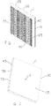
Figure 1 is a schematic isometric angled front view of an exemplary flat panel antenna. -
Figure 2 is a schematic isometric angled back view of the flat panel antenna ofFigure 1 . -
Figure 3 is a schematic isometric exploded view of the antenna ofFigure 1 . -
Figure 4 is a schematic isometric exploded view of the antenna ofFigure 2 . -
Figure 5 is a close-up view of the second side of the intermediate layer ofFigure 3 . -
Figure 6 is a close-up view of the first side of the intermediate layer ofFigure 3 . -
Figure 7 is a close-up view of the second side of the output layer ofFigure 3 . -
Figure 8 is a close-up view of the first side of the output layer ofFigure 3 . -
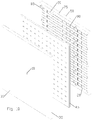
Figure 9 is a schematic isometric angled front view of an alternative waveguide network embodiment of a flat panel antenna. -
Figure 10 is a schematic isometric angled back view of the flat panel antenna ofFigure 9 . -
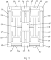
Figure 11 is a schematic top view of the first side of an exemplary segment base. -
Figure 12 is a schematic isometric view of the segment base ofFigure 11 , with a feed tap seated in the feed aperture. -
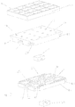
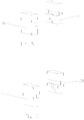
Figure 13 is an exploded angled top isometric view of a flat panel antenna utilizing a single segment pair. -
Figure 14 is an exploded isometric angled bottom view of the flat panel antenna ofFigure 13 . -
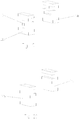
Figure 15 is a schematic isometric view of a feed power divider tap. -
Figure 16 is a schematic isometric view of a central power divider tap. -
Figure 17 is a schematic isometric view of a peripheral power divider tap. -
Figure 18 is a schematic isometric view of a feed tap. -
Figure 19 is a schematic isometric view of a peripheral feed tap. -
Figure 20 is a schematic isometric view of a bypass tap. -
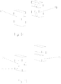
Figure 21 is a schematic isometric view of a 2x2 modular segment with the segment top and one half of the power dividers removed for clarity. -
Figure 22 is a schematic isometric view of a 4x4 modular segment with the segment top and one half of the power dividers removed for clarity. - The inventors have developed a flat panel antenna utilizing a corporate waveguide network and cavity couplers provided in stacked layers. The low loss 4-way coupling of each cavity coupler significantly simplifies the requirements of the corporate waveguide network, enabling higher feed horn density for improved electrical performance. The layered configuration enables cost efficient precision mass production.
- As shown in
Figures 1-8 , a first embodiment of a flatpanel array antenna 1 is formed from several layers, each with surface contours and apertures, combining to form a feed horn array 4 and RF path comprising a series of enclosed coupling cavities and interconnecting waveguides when the layers are stacked upon one another. - The RF path comprises a
waveguide network 5 coupling aninput feed 10 to a plurality ofprimary coupling cavities 15. Each of theprimary coupling cavities 15 is provided with fouroutput ports 20, each of theoutput ports 20 coupled to ahorn radiator 25. - The
input feed 10 is demonstrated positioned generally central on afirst side 30 of aninput layer 35, for example to allow compact mounting of a microwave transceiver thereto, using antenna mounting features (not shown) interchangeable with those used with traditional reflector antennas. Alternatively, theinput feed 10 may be positioned at a layer sidewall 40, between theinput layer 35 and a firstintermediate layer 45, enabling, for example, an antenna side by side with the transceiver configuration where the depth of the resulting flat panel antenna assembly is minimized. - As best shown on
Figures 3 ,4 and6 , thewaveguide network 5 is demonstrated provided on asecond side 50 of theinput layer 35 and afirst side 30 of the firstintermediate layer 45. Thewaveguide network 5 distributes the RF signals to and from theinput feed 10 to a plurality ofprimary coupling cavities 15 provided on asecond side 50 of the firstintermediate layer 45. Thewaveguide network 5 may be dimensioned to provide an equivalent length electrical path to eachprimary coupling cavity 55 to ensure common phase and amplitude. T-type power dividers 55 may be applied to repeatedly divide theinput feed 10 for routing to each of theprimary coupling cavities 15. Thewaveguide sidewalls 60 of the waveguide network may also be provided withsurface features 65 for impedance matching, filters and/or attenuation. - The
waveguide network 5 may be provided with a rectangular waveguide cross section, where a long axis of the rectangular cross section normal to a surface plane of the input layer 35 (seeFigure 6 ). Alternatively, thewaveguide network 5 may be configured such that a long axis of the rectangular cross section is parallel to a surface plane of theinput layer 35. Aseam 70 between theinput layer 35 and the firstintermediate layer 45 may be applied at a midpoint of the waveguide cross section, as shown for example inFigure 6 . Thereby, any leakage and/or dimensional imperfections appearing at the layer joint are at a region of the waveguide cross section where the signal intensity is reduced or minimized. Further, any sidewall draft requirements for manufacture of the layers by injection molding mold separation may be reduced or minimized, as the depth of features formed in either side of the layers is halved. Alternatively, thewaveguide network 5 may be formed on thesecond side 50 of theinput layer 35 or thefirst side 30 of the firstintermediate layer 45 with the waveguide features at full waveguide cross-section depth in one side or the other, and the opposite side operating as the top or bottom sidewall, closing thewaveguide network 5 as the layers are seated upon one another (seeFigures 9 and10 ). - The
primary coupling cavities 15, each fed by a connection to thewaveguide network 5, provide -6 dB coupling to fouroutput ports 20. Theprimary coupling cavities 15 have a rectangular configuration with the waveguide network connection and the fouroutput ports 20 on opposite sides. Theoutput ports 20 are provided on afirst side 30 of anoutput layer 75, each of theoutput ports 20 in communication with one of thehorn radiators 25, thehorn radiators 25 provided as an array ofhorn radiators 25 on asecond side 50 of theoutput layer 75. As shown for example inFigure 5 , thesidewalls 80 of theprimary coupling cavities 15 and/or thefirst side 30 of theoutput layer 75 may be provided with tuning features 85 such asseptums 90 projecting into theprimary coupling cavities 15 or grooves 95 forming a depression to balance transfer between thewaveguide network 5 and theoutput ports 20 of eachprimary coupling cavity 15. The tuning features 85 may be provided symmetrical with one another on opposing surfaces and/or spaced equidistant between theoutput ports 20. - To balance coupling between each of the
output ports 20, each of theoutput ports 20 may be configured as rectangular slots run parallel to a long dimension of the rectangular cavity and the input waveguide. Similarly, the short dimension of theoutput ports 20 may be aligned parallel to the short dimension of the cavity which is parallel to the short dimension of the input waveguide. - When using array element spacing of between 0.75 and 0.95 wavelengths to provide acceptable array directivity, with sufficient defining structure between elements, a cavity aspect ratio, may be, for example, 1.5:1.
- An exemplary cavity may be dimensioned with:
- a depth less than 0.2 wavelengths,
- a width close to n x wavelengths, and
- a length close to n x 3/2 wavelengths.
- The array of
horn radiators 25 on thesecond side 50 of theoutput layer 75 improves directivity (gain), with gain increasing with element aperture until element aperture increases past one wavelength and grating lobes begin to be introduced. One skilled in the art will appreciate that because each of thehorn radiators 20 is individually coupled in phase to theinput feed 10, the prior low density ½ wavelength output slot spacing typically applied to follow propagation peaks within a common feed waveguide slot configuration has been eliminated, allowingcloser horn radiator 20 spacing and thus higher overall antenna gain. - Because an array of
small horn radiators 20 with common phase and amplitude are provided, the amplitude and phase tapers observed in a conventional single large horn configuration that may otherwise require adoption of an excessively deep horn or reflector antenna configuration have been eliminated. - One skilled in the art will appreciate that the simplified geometry of the coupling cavities and corresponding reduction of the waveguide network requirements enables significant simplification of the required layer surface features which reduces overall manufacturing complexity. For example, the input, first intermediate, second intermediate (if present) and
output layers - Although the coupling cavities and waveguides are described as rectangular, for ease of machining and/or mold separation, corners may be radiused and/or rounded in a trade-off between electrical performance and manufacturing efficiency.
- As frequency increases, wavelengths decrease. Therefore, as the desired operating frequency increases, the physical features within a corporate waveguide network, such as steps, tapers and T-type power dividers, become smaller and harder to fabricate. As use of the coupling cavities simplifies the waveguide network requirements, one skilled in the art will appreciate that higher operating frequencies are enabled by the present flat panel antenna, for example up to 26 GHz, above which the required dimension resolution/feature precision may begin to make fabrication with acceptable tolerances cost prohibitive.
- For further ease of cost efficient and/or high precision manufacture, the
input layer 35 andwaveguide network 5 thereon for a plurality of different flat panel antenna configurations may be formed utilizing one or more modular segments. A generally rectangular, such as a square,segment base 103, as shown for example inFigures 11-14 , has afeed aperture 107 andwaveguide network 5. In addition to thefeed aperture 107, thesegment base 103 may be provided with acorner cavity 109 at each corner and atap cavity 111 at a mid-section of each of two opposite sides. A plurality of additional waveguide paths are provided on thefirst side 30 for interconnectingmultiple segment bases 103 to form a waveguide network coupling to a larger number ofoutput ports 20 provided on the corresponding segment tops 121 of adjacent segment bases 103. The additional waveguide paths include acentral waveguide 115 between thefeed aperture 107 and thetap cavities 111, aperipheral waveguide 117 between each of thecorner cavities 109 that are adjacent to one another and afeed waveguide 119 between thefeed aperture 107 and theoutput ports 20 provided on asegment top 121 dimensioned to seat upon thefirst side 30 of thesegment base 103 to form a segment pair 122. - The
segment top 121 may be provided with a mirror image of thewaveguide network 5, thesegment top 121 providing a second half of each of thecentral waveguides 115, and theperipheral waveguides 117 and thefeed waveguides 119 of thesegment base 103. Alternatively, thesegment top 121 may be provided planar, providing the top sidewall of thewaveguide network 5. Thesegment top 121 may be further provided as one of the additional layers of a flat panel antenna configuration, such as a firstintermediate layer 45 or anoutput layer 75 of a flatpanel array antenna 1. Where thesegment top 121 is one of the additional layers of theflat panel antenna 1, a single layer may provide a combined segment top of multiple segment bases 103. - A range of different feed, power divider and bypass taps, for example as shown in
Figures 15-20 , may be seated within thefeed aperture 107 and/or within the apertures formed by adjacent corner or tapcavities waveguide network 5 which links aninput feed 10 of the selectedfeed tap 123 with each of theoutput ports 20 along generally equidistant paths through thewaveguide network 5, to provide uniform phase and signal levels at each of, for example,horn radiators 25 eachoutput port 20 is finally coupled to. To simplify manufacturing requirements, the feed, power and/or bypass taps may be formed in two part form, for example by machining, die casting and/or injection molding. - In a small waveguide network configuration, for example as shown in
Figures 13 and14 , afeed tap 123 dimensioned to couple the input feed 10 to thefeed waveguide 119 is inserted into thefeed aperture 107. Thereby, theinput feed 10 is coupled to the sixteenoutput ports 20 of the segment top and therethrough to the corresponding array ofhorn radiators 25 provided on theexemplary output layer 75. - The segment pairs 122 may alternatively be configured side to side, for example as shown in
Figure 21 , in a 2x2 modular segment embodiment utilizing four segment pairs 122. In the 2x2modular segment 127, thecorner cavities 109 of each of the segment pairs 122 at a center of the 2x2modular segment 127 combine to form a 2x2 feed aperture 129 and thetap cavities 111 of each of the segment pairs 122 adjacent to one another together form 2x2 power divider cavities 131. Aperipheral feed tap 130 is inserted in the 2x2 feed aperture 129, provided with aninput feed 10 coupled to a centralpower divider tap 135 provided in each of the 2x2 power divider cavities 131 via at least one of theperipheral waveguides 117 there between. The central power divider taps 135 are coupled to feed power divider taps 133 provided in each of thefeed apertures 107 of each segment pair 122 via thecentral waveguide 115 therebetween. The feed power divider taps 133 are coupled to theoutput ports 20 of each segment pair 122 via thefeed waveguide 119. Thereby, a signal provided at theinput feed 10 is distributed to each of the combined sixty-fouroutput ports 20 of the corresponding segment tops 121. - An even
larger waveguide network 5 may be formed from segment pairs 122, for example, by interconnecting sixteen of the segment pairs 122 in a side to side matrix to form a generally planar 4x4 modular segment, for example as shown inFigure 22 . Details of the 4x4modular segment 137 and the interconnections forming thewaveguide network 5 thereof will be described with respect to grouping four 2x2modular segments 127, as described herein above, together. The generally planar 4x4 matrix of segment pairs 122 has a 4x4 feed aperture 139 defined by the combinedcorner cavities 109 of the segment pairs 122 at the center of the4x4 modular.segment 137. The tap cavities 111 of the segment pairs 122 adjacent the center of the 4x4modular segment 137 combine to form bypass cavities 141 and thecorner cavities 109 of the segment pairs 122 adjacent the bypass cavities 141 and in-line with the 4x4 feed aperture 139, form 4x4 power divider cavities 143. - A
peripheral feed tap 130 with aninput feed 10 is seated within the 4x4 feed aperture 139. Theperipheral feed tap 130 is coupled to a bypass tap 145 (seeFigure 20 ) provided in each of the bypass cavities 141 via at least one of theperipheral waveguides 117 there between. A peripheralpower divider tap 151 is seated in each of the 4x4 power divider cavities 143; the peripheral power divider taps 151 and coupled to the respective bypass taps 145 via at least one of theperipheral waveguides 117 there between. - The corner cavities 109 of each of the segment pairs 122 at a center of each of the 2x2
modular segments 127 combine to form a 2x2 feed aperture 129 and thetap cavities 111 of each of the segment pairs 122 adjacent to one another in each 2x2modular segment 127 together form a 2x2 power divider cavity 131. - Another peripheral
power divider tap 151 is provided in each 2x2 feed aperture 129, coupling with the peripheralpower divider tap 151 of the 4x4 power divider cavities 143 via theperipheral waveguide 117 there between. The peripheral power divider taps 151 of the 2x2 feed apertures 129 are coupled to the central power divider taps 135 seated in the 2x2 power divider cavities by at least one of theperipheral waveguides 117 there between. The central power divider taps 135 are each coupled to a feedpower divider tap 133 provided in each of the 2x2 power divider cavities 131 via thecentral waveguide 115 there between. The feed power divider taps 133 are coupled to theoutput ports 20 of each segment pair 122 via thefeed waveguide 119 there between. Thereby, a signal provided at theinput feed 10 is distributed to each of the combined two hundred and fifty-sixoutput ports 20 of the corresponding segment tops 121. - The precision alignment and/or mechanical interconnection of the segment pairs 122 with one another and/or with adjacent equipment and/or further layers may be simplified by providing retention features 153 along a periphery of the segment pair 122. For example as shown in
Figures 11 and12 , the retention features 153 may be provided ascomplementary tabs 155 andslots 157 enabling snap together interconnection with each other and/or corresponding tabs and slots provided in surrounding elements, such as a frame and/or radome. - One skilled in the art will appreciate that selection of the feed, power divider and/or bypass taps to interconnect a waveguide path along segment pairs 122 each with an identical array of available waveguide channels enables generation of a waveguide path between the
feed aperture 107 and each of theoutput ports 20 that has a generally equivalent length. Thereby, phase and/or signal strength errors generated by the division of the input signal to each of theoutput ports 20 may be avoided. - The use of segment pairs 122 may significantly simplify manufacturing requirements of the
flat panel antenna 1. Thesegment base 103 andsegment top 121 may be formed, for example, by machining, die casting and/or injection molding. A polymer material machined and/or injection moldedsegment base 103 and/orsegment top 121 may be metalized or metal coated. - One skilled in the art will appreciate that fabrication of a
universal segment base 103 and/orsegment top 121 may reduce duplicate tooling and quality control requirements for a family of flat panel antennas. Where machining is applied, the segment pairs 122 may be formed via smaller pieces of stock material, reducing material costs and enabling a smaller required range of motion from the machining tool(s). Where fabrication via die casting and/or injection molding is applied, the die size and complexity of the die may be reduced. Further, with a smaller die and/or mold requirement, the separation characteristics are improved which may reduce the compromises required with respect to mold draft requirements. Where a further metal coating and/or metalizing step is applied to a, for example, polymer injection molded base component, such may be similarly simplified by being applied to a smaller total area. - From the foregoing, it will be apparent that the present invention brings to the art a modular feed network usable, for example, as the
waveguide network 5 of a high performance flat panel antenna with reduced cross section that is strong, lightweight and may be repeatedly cost efficiently manufactured with a high level of precision. Utilizing segment pairs 122 to form thewaveguide network 5 further may enable fabrication of asingle segment base 103 and/orsegment top 121 cost efficiently and with improved precision. Where the segment pairs 122 are formed via die casting or injection molding, the single die and/or mold required for manufacture of a family of antennas is simplified and the reduced size of such may simplify mold separation and thus draft requirements of the waveguide network features, improving the cross section of the waveguide and thereby overall electrical performance.Table of Parts 1 flat panel array antenna 5 waveguide network 10 input feed 15 primary coupling cavity 20 output port 25 horn radiator 30 first side 35 input layer 40 layer sidewall 45 first intermediate layer 50 second side 55 T- type power divider 60 waveguide sidewalls 65 surface features 70 seam 75 output layer 80 sidewall 85 tuning feature 90 septum 95 groove 103 segment base 107 feed aperture 109 corner cavity 111 tap cavity 115 central waveguide 117 peripheral waveguide 119 feed waveguide 121 segment top 122 segment pair 123 feed tap 127 2x2 modular segment 129 2x2 feed aperture 130 peripheral feed tap 131 2x2 power divider cavity 133 feed power divider tap 135 central power divider tap 137 4x4 modular segment 139 4x4 feed aperture 141 bypass cavity 143 4x4 power divider cavity 145 bypass tap 151 peripheral power divider tap 153 retention feature 155 tab 157 slot - Where in the foregoing description reference has been made to materials, ratios, integers or components having known equivalents then such equivalents are herein incorporated as if individually set forth.
- While the present invention has been illustrated by the description of the embodiments thereof, and while the embodiments have been described in considerable detail, it is not the intention of the applicant to restrict or in any way limit the scope of the appended claims to such detail. Additional advantages and modifications will readily appear to those skilled in the art. Therefore, the invention in its broader aspects is not limited to the specific details, representative apparatus, methods, and illustrative examples shown and described. Accordingly, departures may be made from such details without departure from the spirit or scope of applicant's general inventive concept. Further, it is to be appreciated that improvements and/or modifications may be made thereto without departing from the scope or spirit of the present invention as defined by the following claims.
Claims (15)
- A modular feed network, comprising:a generally rectangular segment base (103) provided with a feed aperture (107); the segment base (103) having a corner cavity (109) at each corner and a tap cavity (111) at a mid-section of each of two opposite sides; anda segment top (121) provided with a plurality of output ports (20); the segment top (121) provided seated upon a first side of the segment base (103) to form a segment pair (122);the segment base (103) provided with a central waveguide (115), on the first side, between the feed aperture (107) and the tap cavities (111);the segment base (103) provided with a peripheral waveguide (117), on the first side, between each of the corner cavities (109) that are adjacent to one another;the segment base (103) provided with a feed waveguide (119) between the feed aperture (107) and the output ports (20).
- The modular feed network of claim 1, wherein a path between the feed aperture (107) and each of the output ports (20) has a generally equivalent length.
- The modular feed network of claim 1, further including retention features (153) provided on a periphery of the segment pair (122); the retention features (153) dimensioned for mechanical coupling of the segment pair (122) to additional segment pairs (122), side to side.
- The modular feed network of claim 1, wherein the segment top (121) is provided with a mirror image waveguide network (5); the mirror image waveguide network (5) providing a second half of each of the central waveguide (115), the peripheral waveguide (117) and the feed waveguide (119) of the segment base (103).
- The modular feed network of claim 1, wherein the segment top (121) is a first intermediate layer (45) of a flat panel array antenna.
- The modular feed network of claim 1, wherein the segment top (121) is an output layer (75) of a flat panel array antenna.
- The modular feed network of claim 1, wherein there are four segment pairs (122) arranged side-to-side to form a generally planar 2x2 modular segment (127).
- The modular feed network of claim 7, wherein the corner cavities (109) of each of the segment pairs (122) at a center of the 2x2 modular segment (127) combine to form a 2x2 feed aperture (129);
the tap cavities (111) of each of the segment pairs (122) adjacent to one another together forming a 2x2 power divider cavity (131);
a peripheral feed tap (130) provided in the 2x2 feed aperture; the peripheral feed tap (130) provided with an input feed (10) coupled to a feed power divider tap (133) provided in each of the 2x2 power divider cavities (131) via at least one of the peripheral waveguides (117) therebetween;
the feed power divider taps (133) coupled to a central power divider tap (135) provided in each of the feed apertures (107) of each segment pair (122) via the central waveguide (115) therebetween;
the central power divider taps (135) coupled to the output ports (20) of each segment pair (122) via the feed waveguide (119). - The modular feed network of claim 7, wherein there are four 2x2 modular segments (127) arranged side by side to form a generally planar 4x4 modular segment (137).
- The modular feed network of claim 9, wherein the corner cavities (109) of each of the segment pairs (122) at a center of the 4x4 modular segment (137) combine to form a 4x4 feed aperture (139);
the tap cavities (111) of the segment pairs (122) adjacent the center of the 4x4 modular segment (137) combine to form bypass cavities (141);
the corner cavities (109) of the segment pairs (122) adjacent the bypass cavities (141) and in-line with the 4x4 feed aperture (139), forming 4x4 power divider cavities (143);
the corner cavities (109) of each of the segment pairs (122) at a center of each of the 2x2 modular segments (127) combine to form a 2x2 feed aperture (129);
the tap cavities (111) of each of the segment pairs (122) adjacent to one another in each 2x2 modular segment (127) together forming a 2x2 power divider cavity (131);
a peripheral feed tap (130) provided in the 4x4 feed aperture (139); the peripheral feed tap (130) provided with an input feed (10) coupled to a bypass tap (145) provided in each of the bypass cavities (141) via at least one of the peripheral waveguides (117) therebetween;
a peripheral power divider tap (151) provided in each of the 4x4 power divider cavities (143) and the 2x2 power divider cavities (131);
the peripheral power divider tap (151) of the 4x4 power divider cavities (143) coupled to the bypass taps (145) via at least one of the peripheral waveguides (117) therebetween;
the peripheral power divider taps (151) of the 4x4 power divider cavities (143) coupled to the peripheral power divider taps (151) of the 2x2 feed aperture (129) via at least one of the periphery waveguides (117) therebetween;
the peripheral power divider tap (151) of the 2x2 feed aperture (129) coupled to a central power tap (135) provided in each of the 2x2 power divider cavities (131) via the peripheral waveguides (117) therebetween;
the central power divider taps (135) coupled to a feed power divider tap (133) provided in each of the feed apertures (107) of each of the segment pairs (122) via the central waveguide (115) therebetween;
the central feed taps coupled to the output ports (20) of each segment pair (122) via the feed waveguide (119) therebetween. - A method for manufacture of a modular feed network, comprising:forming a generally rectangular segment base (103) provided with a feed aperture (107); providing the segment base (103) with a corner cavity (109) at each corner of the segment base (103) and a tap cavity (111) of the segment base (103) provided at a mid-section of each of two opposite sides of the segment base (103); andforming a segment top (121) provided with a plurality of output ports (20); andseating the segment top (121) upon a first side of the segment base (103) to form a segment pair (122);the segment base (103) provided with a central waveguide (115), on the first side, between the feed aperture (107) and the tap cavities (111);the segment base (103) provided with a peripheral waveguide (117), on the first side, between each of the corner cavities (109) that are adjacent to one another;the segment base (103) provided with a feed waveguide (119) between the feed aperture (107) and the output ports (20).
- The method of claim 11, wherein the segment base (103) is formed via injection molding.
- The method of claim 11, wherein the segment base (103) is formed via die casting.
- The method of claim 11, further including the step of arranging four segment pairs (103) side-to-side to form a generally planar 2x2 modular segment (127).
- The method of claim 14, further including the step of arranging four of the 2x2 modular segments (127) side by side to form a generally planar 4x4 modular segment (137).
Applications Claiming Priority (3)
| Application Number | Priority Date | Filing Date | Title |
|---|---|---|---|
| US13/297,304 US8558746B2 (en) | 2011-11-16 | 2011-11-16 | Flat panel array antenna |
| US13/677,862 US8866687B2 (en) | 2011-11-16 | 2012-11-15 | Modular feed network |
| PCT/US2012/065427 WO2013074872A1 (en) | 2011-11-16 | 2012-11-16 | Modular feed network |
Publications (3)
| Publication Number | Publication Date |
|---|---|
| EP2780982A1 EP2780982A1 (en) | 2014-09-24 |
| EP2780982A4 EP2780982A4 (en) | 2015-07-29 |
| EP2780982B1 true EP2780982B1 (en) | 2017-03-29 |
Family
ID=48280072
Family Applications (1)
| Application Number | Title | Priority Date | Filing Date |
|---|---|---|---|
| EP12849231.1A Not-in-force EP2780982B1 (en) | 2011-11-16 | 2012-11-16 | Modular feed network |
Country Status (7)
| Country | Link |
|---|---|
| US (1) | US8866687B2 (en) |
| EP (1) | EP2780982B1 (en) |
| CN (1) | CN103918128B (en) |
| BR (1) | BR112014011114B1 (en) |
| IN (1) | IN2014DN03448A (en) |
| MX (1) | MX2014005727A (en) |
| WO (1) | WO2013074872A1 (en) |
Families Citing this family (70)
| Publication number | Priority date | Publication date | Assignee | Title |
|---|---|---|---|---|
| EP2110884B1 (en) * | 2008-04-15 | 2013-05-29 | Sub10 Systems Limited | Surface-mountable antenna with waveguide connector function, communication system, adaptor and arrangement comprising the antenna device |
| US8988294B2 (en) * | 2011-12-06 | 2015-03-24 | Viasat, Inc. | Antenna with integrated condensation control system |
| US10312715B2 (en) | 2015-09-16 | 2019-06-04 | Energous Corporation | Systems and methods for wireless power charging |
| US10992185B2 (en) | 2012-07-06 | 2021-04-27 | Energous Corporation | Systems and methods of using electromagnetic waves to wirelessly deliver power to game controllers |
| US10965164B2 (en) | 2012-07-06 | 2021-03-30 | Energous Corporation | Systems and methods of wirelessly delivering power to a receiver device |
| US9825674B1 (en) | 2014-05-23 | 2017-11-21 | Energous Corporation | Enhanced transmitter that selects configurations of antenna elements for performing wireless power transmission and receiving functions |
| US11502551B2 (en) | 2012-07-06 | 2022-11-15 | Energous Corporation | Wirelessly charging multiple wireless-power receivers using different subsets of an antenna array to focus energy at different locations |
| US12057715B2 (en) | 2012-07-06 | 2024-08-06 | Energous Corporation | Systems and methods of wirelessly delivering power to a wireless-power receiver device in response to a change of orientation of the wireless-power receiver device |
| US10992187B2 (en) | 2012-07-06 | 2021-04-27 | Energous Corporation | System and methods of using electromagnetic waves to wirelessly deliver power to electronic devices |
| US10256657B2 (en) | 2015-12-24 | 2019-04-09 | Energous Corporation | Antenna having coaxial structure for near field wireless power charging |
| US9190739B2 (en) * | 2013-06-24 | 2015-11-17 | Delphi Technologies, Inc. | Antenna with fifty percent overlapped subarrays |
| FI127914B (en) * | 2014-08-21 | 2019-05-15 | Stealthcase Oy | Device and method for guiding electromagnetic waves |
| KR102302466B1 (en) * | 2014-11-11 | 2021-09-16 | 주식회사 케이엠더블유 | Waveguide slotted array antenna |
| WO2016145395A1 (en) * | 2015-03-12 | 2016-09-15 | Custom Microwave, Inc. | Methods and apparatus for multiple beam antenna structures |
| US9876282B1 (en) * | 2015-04-02 | 2018-01-23 | Waymo Llc | Integrated lens for power and phase setting of DOEWG antenna arrays |
| US9640847B2 (en) | 2015-05-27 | 2017-05-02 | Viasat, Inc. | Partial dielectric loaded septum polarizer |
| US9859597B2 (en) | 2015-05-27 | 2018-01-02 | Viasat, Inc. | Partial dielectric loaded septum polarizer |
| US9559428B1 (en) | 2015-08-25 | 2017-01-31 | Viasat, Inc. | Compact waveguide power combiner/divider for dual-polarized antenna elements |
| CN106486721B (en) | 2015-08-28 | 2021-04-16 | 康普技术有限责任公司 | Phase shifter assembly |
| US11710321B2 (en) | 2015-09-16 | 2023-07-25 | Energous Corporation | Systems and methods of object detection in wireless power charging systems |
| US10778041B2 (en) | 2015-09-16 | 2020-09-15 | Energous Corporation | Systems and methods for generating power waves in a wireless power transmission system |
| US10734717B2 (en) * | 2015-10-13 | 2020-08-04 | Energous Corporation | 3D ceramic mold antenna |
| US10063108B1 (en) | 2015-11-02 | 2018-08-28 | Energous Corporation | Stamped three-dimensional antenna |
| US11863001B2 (en) | 2015-12-24 | 2024-01-02 | Energous Corporation | Near-field antenna for wireless power transmission with antenna elements that follow meandering patterns |
| US10038332B1 (en) | 2015-12-24 | 2018-07-31 | Energous Corporation | Systems and methods of wireless power charging through multiple receiving devices |
| US10079515B2 (en) | 2016-12-12 | 2018-09-18 | Energous Corporation | Near-field RF charging pad with multi-band antenna element with adaptive loading to efficiently charge an electronic device at any position on the pad |
| US10082570B1 (en) * | 2016-02-26 | 2018-09-25 | Waymo Llc | Integrated MIMO and SAR radar antenna architecture for self driving cars |
| EP3430684B1 (en) | 2016-03-15 | 2022-06-15 | Commscope Technologies LLC | Flat panel array antenna with integrated polarization rotator |
| CN109314291B (en) | 2016-06-17 | 2020-11-27 | 康普技术有限责任公司 | Phased Array Antenna with Multistage Phase Shifters |
| US10539656B2 (en) * | 2016-07-21 | 2020-01-21 | Waymo Llc | Antenna and radar system that include a polarization-rotating layer |
| US11309619B2 (en) | 2016-09-23 | 2022-04-19 | Intel Corporation | Waveguide coupling systems and methods |
| WO2018057006A1 (en) | 2016-09-23 | 2018-03-29 | Intel Corporation | Semiconductor package including a modular side radiating waveguide launcher |
| US10566672B2 (en) | 2016-09-27 | 2020-02-18 | Intel Corporation | Waveguide connector with tapered slot launcher |
| US10256521B2 (en) | 2016-09-29 | 2019-04-09 | Intel Corporation | Waveguide connector with slot launcher |
| US11394094B2 (en) | 2016-09-30 | 2022-07-19 | Intel Corporation | Waveguide connector having a curved array of waveguides configured to connect a package to excitation elements |
| US10923954B2 (en) | 2016-11-03 | 2021-02-16 | Energous Corporation | Wireless power receiver with a synchronous rectifier |
| JP6691273B2 (en) | 2016-12-12 | 2020-04-28 | エナージャス コーポレイション | A method for selectively activating the antenna area of a near-field charging pad to maximize delivered wireless power |
| US10680319B2 (en) | 2017-01-06 | 2020-06-09 | Energous Corporation | Devices and methods for reducing mutual coupling effects in wireless power transmission systems |
| US10439442B2 (en) | 2017-01-24 | 2019-10-08 | Energous Corporation | Microstrip antennas for wireless power transmitters |
| WO2018183892A1 (en) | 2017-03-30 | 2018-10-04 | Energous Corporation | Flat antennas having two or more resonant frequencies for use in wireless power transmission systems |
| US12074452B2 (en) | 2017-05-16 | 2024-08-27 | Wireless Electrical Grid Lan, Wigl Inc. | Networked wireless charging system |
| US11462949B2 (en) | 2017-05-16 | 2022-10-04 | Wireless electrical Grid LAN, WiGL Inc | Wireless charging method and system |
| US12074460B2 (en) | 2017-05-16 | 2024-08-27 | Wireless Electrical Grid Lan, Wigl Inc. | Rechargeable wireless power bank and method of using |
| CN107342454B (en) * | 2017-06-09 | 2020-02-21 | 宁波大学 | A waveguide slot array antenna |
| US10848853B2 (en) | 2017-06-23 | 2020-11-24 | Energous Corporation | Systems, methods, and devices for utilizing a wire of a sound-producing device as an antenna for receipt of wirelessly delivered power |
| US11342798B2 (en) | 2017-10-30 | 2022-05-24 | Energous Corporation | Systems and methods for managing coexistence of wireless-power signals and data signals operating in a same frequency band |
| USD881854S1 (en) * | 2017-12-29 | 2020-04-21 | Waymo Llc | Integrated MIMO and SAR radar antenna |
| US10468737B2 (en) * | 2017-12-30 | 2019-11-05 | Intel Corporation | Assembly and manufacturing friendly waveguide launchers |
| US11199611B2 (en) * | 2018-02-20 | 2021-12-14 | Magna Electronics Inc. | Vehicle radar system with T-shaped slot antennas |
| US11355859B2 (en) * | 2018-06-12 | 2022-06-07 | Metawave Corporation | Metamatertial, antenna array having an aperture layer |
| US11437735B2 (en) | 2018-11-14 | 2022-09-06 | Energous Corporation | Systems for receiving electromagnetic energy using antennas that are minimally affected by the presence of the human body |
| US11539243B2 (en) | 2019-01-28 | 2022-12-27 | Energous Corporation | Systems and methods for miniaturized antenna for wireless power transmissions |
| CN113661660B (en) | 2019-02-06 | 2023-01-24 | 艾诺格思公司 | Method for estimating optimal phase, wireless power transmitting device and storage medium |
| US12155231B2 (en) | 2019-04-09 | 2024-11-26 | Energous Corporation | Asymmetric spiral antennas for wireless power transmission and reception |
| CN110364828A (en) * | 2019-08-13 | 2019-10-22 | 嘉兴毫微科技有限公司 | Millimeter wave high gain array antenna |
| US11411441B2 (en) | 2019-09-20 | 2022-08-09 | Energous Corporation | Systems and methods of protecting wireless power receivers using multiple rectifiers and establishing in-band communications using multiple rectifiers |
| WO2021055898A1 (en) | 2019-09-20 | 2021-03-25 | Energous Corporation | Systems and methods for machine learning based foreign object detection for wireless power transmission |
| US11381118B2 (en) | 2019-09-20 | 2022-07-05 | Energous Corporation | Systems and methods for machine learning based foreign object detection for wireless power transmission |
| WO2021055900A1 (en) | 2019-09-20 | 2021-03-25 | Energous Corporation | Classifying and detecting foreign objects using a power amplifier controller integrated circuit in wireless power transmission systems |
| WO2021055901A1 (en) | 2019-09-20 | 2021-03-25 | Energous Corporation | Asymmetric spiral antennas with parasitic elements for wireless power transmission |
| US11355966B2 (en) | 2019-12-13 | 2022-06-07 | Energous Corporation | Charging pad with guiding contours to align an electronic device on the charging pad and efficiently transfer near-field radio-frequency energy to the electronic device |
| US10985617B1 (en) | 2019-12-31 | 2021-04-20 | Energous Corporation | System for wirelessly transmitting energy at a near-field distance without using beam-forming control |
| US11799324B2 (en) | 2020-04-13 | 2023-10-24 | Energous Corporation | Wireless-power transmitting device for creating a uniform near-field charging area |
| US11469629B2 (en) | 2020-08-12 | 2022-10-11 | Energous Corporation | Systems and methods for secure wireless transmission of power using unidirectional communication signals from a wireless-power-receiving device |
| CN112186340B (en) * | 2020-09-29 | 2023-11-07 | 京东方科技集团股份有限公司 | Antenna and method of making same |
| US12306285B2 (en) | 2020-12-01 | 2025-05-20 | Energous Corporation | Systems and methods for using one or more sensors to detect and classify objects in a keep-out zone of a wireless-power transmission field, and antennas with integrated sensor arrangements |
| US11916398B2 (en) | 2021-12-29 | 2024-02-27 | Energous Corporation | Small form-factor devices with integrated and modular harvesting receivers, and shelving-mounted wireless-power transmitters for use therewith |
| US12142939B2 (en) | 2022-05-13 | 2024-11-12 | Energous Corporation | Integrated wireless-power-transmission platform designed to operate in multiple bands, and multi-band antennas for use therewith |
| US12355149B1 (en) * | 2023-06-06 | 2025-07-08 | Utah State University Space Dynamics Laboratory | Waveguide horn antenna |
| US12586915B2 (en) * | 2024-08-19 | 2026-03-24 | Nxp B.V. | Antenna assembly with metallized cavity waveguide |
Family Cites Families (81)
| Publication number | Priority date | Publication date | Assignee | Title |
|---|---|---|---|---|
| US2573746A (en) | 1945-09-19 | 1951-11-06 | Honorary Advisory Council Sci | Directive antenna for microwaves |
| US2981948A (en) | 1956-05-29 | 1961-04-25 | Hughes Aircraft Co | Simultaneous lobing array antenna system |
| US3157847A (en) | 1961-07-11 | 1964-11-17 | Robert M Williams | Multilayered waveguide circuitry formed by stacking plates having surface grooves |
| US3243818A (en) | 1962-08-22 | 1966-03-29 | Hughes Aircraft Co | Dual band slot antenna having common waveguide with differing slots, each individualto its own band |
| US3281851A (en) | 1963-05-24 | 1966-10-25 | Hughes Aircraft Co | Dual mode slot antenna |
| US3193830A (en) | 1963-07-25 | 1965-07-06 | Joseph H Provencher | Multifrequency dual ridge waveguide slot antenna |
| US3701162A (en) | 1964-03-24 | 1972-10-24 | Hughes Aircraft Co | Planar antenna array |
| US3340534A (en) | 1965-09-22 | 1967-09-05 | Hughes Aircraft Co | Elliptically or circularly polarized antenna |
| GB1200058A (en) | 1967-04-17 | 1970-07-29 | Elliott Brothers London Ltd | Improvements relating to aerials |
| US3599216A (en) | 1969-08-11 | 1971-08-10 | Nasa | Virtual-wall slot circularly polarized planar array antenna |
| US4121220A (en) | 1975-01-31 | 1978-10-17 | Electronique Marcel Dassault | Flat radar antenna employing circular array of slotted waveguides |
| US3999151A (en) | 1975-09-08 | 1976-12-21 | Western Electric Company, Inc. | Crossguide hybrid coupler and a commutating hybrid using same to form a channel branching network |
| US4429313A (en) | 1981-11-24 | 1984-01-31 | Muhs Jr Harvey P | Waveguide slot antenna |
| FR2523376A1 (en) | 1982-03-12 | 1983-09-16 | Labo Electronique Physique | RADIATION ELEMENT OR HYPERFREQUENCY SIGNAL RECEIVER WITH LEFT AND RIGHT CIRCULAR POLARIZATIONS AND FLAT ANTENNA COMPRISING A NETWORK OF SUCH JUXTAPOSED ELEMENTS |
| US4949092A (en) | 1984-11-08 | 1990-08-14 | Highes Aircraft Company | Modularized contoured beam direct radiating antenna |
| US4716415A (en) | 1984-12-06 | 1987-12-29 | Kelly Kenneth C | Dual polarization flat plate antenna |
| US5019831A (en) | 1985-05-20 | 1991-05-28 | Texas Instruments Incorporated | Dual end resonant slot array antenna feed having a septum |
| FR2592232B1 (en) | 1985-12-20 | 1988-02-12 | Radiotechnique Compelec | MICROWAVE PLANE ANTENNA WITH SUSPENDED SUBSTRATE LINES ARRAY AND METHOD FOR MANUFACTURING THE SAME. |
| US4679011A (en) | 1986-03-21 | 1987-07-07 | Rca Corporation | Waveguide directional coupler family with a common housing having different sets of conductive block insertable therein |
| US5086304A (en) | 1986-08-13 | 1992-02-04 | Integrated Visual, Inc. | Flat phased array antenna |
| GB8619680D0 (en) | 1986-08-13 | 1986-09-24 | Collins J L F C | Flat plate array |
| US4829309A (en) | 1986-08-14 | 1989-05-09 | Matsushita Electric Works, Ltd. | Planar antenna |
| JPH01103006A (en) | 1987-10-15 | 1989-04-20 | Matsushita Electric Works Ltd | Plane antenna |
| US4812788A (en) | 1987-11-02 | 1989-03-14 | Hughes Aircraft Company | Waveguide matrix including in-plane crossover |
| JP2733472B2 (en) | 1988-02-19 | 1998-03-30 | 有限会社ラジアルアンテナ研究所 | Waveguide slot antenna, method of manufacturing the same, and waveguide coupling structure |
| US5210543A (en) | 1988-12-20 | 1993-05-11 | Hughes Aircraft Company | Feed waveguide for an array antenna |
| US5270721A (en) | 1989-05-15 | 1993-12-14 | Matsushita Electric Works, Ltd. | Planar antenna |
| US5321411A (en) | 1990-01-26 | 1994-06-14 | Matsushita Electric Works, Ltd. | Planar antenna for linearly polarized waves |
| US5010351A (en) | 1990-02-08 | 1991-04-23 | Hughes Aircraft Company | Slot radiator assembly with vane tuning |
| US4985708A (en) | 1990-02-08 | 1991-01-15 | Hughes Aircraft Company | Array antenna with slot radiators offset by inclination to eliminate grating lobes |
| FR2669776B1 (en) | 1990-11-23 | 1993-01-22 | Thomson Csf | SLOTTED MICROWAVE ANTENNA WITH LOW THICKNESS STRUCTURE. |
| SE469540B (en) | 1991-11-29 | 1993-07-19 | Ericsson Telefon Ab L M | GUIDANCE GUARANTEE WITH TARGETED HALL ROOM GUARD |
| US5247268A (en) | 1992-01-06 | 1993-09-21 | General Electric Company | Adjustable waveguide branch, and directional coupler |
| US5243354A (en) | 1992-08-27 | 1993-09-07 | The United States Of America As Represented By The Secretary Of The Army | Microstrip electronic scan antenna array |
| US5327150A (en) | 1993-03-03 | 1994-07-05 | Hughes Aircraft Company | Phased array antenna for efficient radiation of microwave and thermal energy |
| JPH07106847A (en) | 1993-10-07 | 1995-04-21 | Nippon Steel Corp | Leaky Waveguide Slot Array Antenna |
| SE510082C2 (en) | 1993-11-30 | 1999-04-19 | Saab Ericsson Space Ab | Waveguide antenna with transverse and longitudinal slots |
| US5512906A (en) | 1994-09-12 | 1996-04-30 | Speciale; Ross A. | Clustered phased array antenna |
| US5589843A (en) | 1994-12-28 | 1996-12-31 | Radio Frequency Systems, Inc. | Antenna system with tapered aperture antenna and microstrip phase shifting feed network |
| RU2083035C1 (en) | 1995-06-05 | 1997-06-27 | Александр Данилович Христич | High-frequency planar-array antenna |
| US5650793A (en) | 1995-06-06 | 1997-07-22 | Hughes Missile Systems Company | Centered longitudinal series/series coupling slot for coupling energy between a boxed stripline and a crossed rectangular waveguide and antenna array employing same |
| US5619216A (en) | 1995-06-06 | 1997-04-08 | Hughes Missile Systems Company | Dual polarization common aperture array formed by waveguide-fed, planar slot array and linear short backfire array |
| FI99221C (en) | 1995-08-25 | 1997-10-27 | Nokia Telecommunications Oy | Planar antenna construction |
| GB9703748D0 (en) | 1997-02-22 | 1997-04-09 | Fortel International Limited | Microwave antennas |
| FR2764738B1 (en) | 1997-06-13 | 1999-08-27 | Thomson Csf | INTEGRATED TRANSMISSION OR RECEPTION DEVICE |
| US6028562A (en) | 1997-07-31 | 2000-02-22 | Ems Technologies, Inc. | Dual polarized slotted array antenna |
| US6101705A (en) | 1997-11-18 | 2000-08-15 | Raytheon Company | Methods of fabricating true-time-delay continuous transverse stub array antennas |
| US5880695A (en) | 1998-02-05 | 1999-03-09 | Astron Corporation | Antenna system for wireless comunication systems |
| SE513586C2 (en) | 1998-05-12 | 2000-10-02 | Ericsson Telefon Ab L M | Method of producing an antenna structure and antenna structure prepared by said method |
| US7577398B2 (en) | 2000-01-14 | 2009-08-18 | Andrew Llc | Repeaters for wireless communication systems |
| US6201508B1 (en) | 1999-12-13 | 2001-03-13 | Space Systems/Loral, Inc. | Injection-molded phased array antenna system |
| DE60044826D1 (en) | 2000-04-18 | 2010-09-23 | Hitachi Chemical Co Ltd | PLANAR ANTENNA FOR BEAM SCANNING |
| US6297782B1 (en) | 2000-07-26 | 2001-10-02 | Gabriel Electronics Incorporated | Modular hub array antenna |
| US6304228B1 (en) | 2000-10-06 | 2001-10-16 | Space Systems/Loral, Inc. | Stepped waveguide slot array with phase control and satellite communication system employing same |
| JP4021150B2 (en) | 2001-01-29 | 2007-12-12 | 沖電気工業株式会社 | Slot array antenna |
| EP1371112B1 (en) | 2001-03-21 | 2007-05-02 | Microface Co. Ltd | Waveguide slot antenna and manufacturing method thereof |
| US6476772B1 (en) | 2001-04-16 | 2002-11-05 | Space Systems/Loral, Inc. | Waveguide slot array capable of radiating shaped beams |
| US7680516B2 (en) | 2001-05-02 | 2010-03-16 | Trex Enterprises Corp. | Mobile millimeter wave communication link |
| DE10126468B4 (en) | 2001-05-31 | 2007-07-05 | Eads Deutschland Gmbh | slot antenna |
| US6731241B2 (en) | 2001-06-13 | 2004-05-04 | Raytheon Company | Dual-polarization common aperture antenna with rectangular wave-guide fed centered longitudinal slot array and micro-stripline fed air cavity back transverse series slot array |
| US6624787B2 (en) | 2001-10-01 | 2003-09-23 | Raytheon Company | Slot coupled, polarized, egg-crate radiator |
| JP3928035B2 (en) | 2001-12-27 | 2007-06-13 | 株式会社エッチ・ケー・エス | Turbocharger |
| US6950066B2 (en) | 2002-08-22 | 2005-09-27 | Skycross, Inc. | Apparatus and method for forming a monolithic surface-mountable antenna |
| US7227508B2 (en) | 2004-01-07 | 2007-06-05 | Motia Inc. | Vehicle mounted satellite antenna embedded within moonroof or sunroof |
| US7391381B2 (en) | 2004-01-07 | 2008-06-24 | Motia | Vehicle mounted satellite antenna system with in-motion tracking using beam forming |
| US6977621B2 (en) | 2004-01-07 | 2005-12-20 | Motia, Inc. | Vehicle mounted satellite antenna system with inverted L-shaped waveguide |
| WO2005079158A2 (en) | 2004-02-23 | 2005-09-01 | Galtronics Ltd. | Conical beam cross-slot antenna |
| US7205948B2 (en) | 2005-05-24 | 2007-04-17 | Raytheon Company | Variable inclination array antenna |
| CN1885616A (en) * | 2005-06-23 | 2006-12-27 | 北京海域天华通讯设备有限公司 | High-gain waveguide trumpet array flat antenna |
| IL174549A (en) | 2005-10-16 | 2010-12-30 | Starling Advanced Comm Ltd | Dual polarization planar array antenna and cell elements therefor |
| JP4822262B2 (en) | 2006-01-23 | 2011-11-24 | 沖電気工業株式会社 | Circular waveguide antenna and circular waveguide array antenna |
| GB2434923A (en) | 2006-02-03 | 2007-08-08 | Ericsson Telefon Ab L M | Antenna feed device using two separate L-shaped waveguides to give an overall T-shape |
| GB2434922A (en) | 2006-02-03 | 2007-08-08 | Ericsson Telefon Ab L M | Ortho-mode transducer connecting two rectangular waveguides to a common circular waveguide |
| JP4394147B2 (en) | 2006-02-06 | 2010-01-06 | 三菱電機株式会社 | High frequency module |
| KR100721871B1 (en) | 2006-05-23 | 2007-05-25 | 위월드 주식회사 | Waveguide slot array antenna for satellite signal reception with arbitrary linear polarization |
| USD576344S1 (en) | 2006-08-01 | 2008-09-02 | Lowel-Light Manufacturing, Inc. | Male pin holder for lighting fixture |
| CN101000981A (en) * | 2007-01-16 | 2007-07-18 | 北京海域天华通讯设备有限公司 | Waveguide slot array antenna |
| CN201060943Y (en) * | 2007-07-10 | 2008-05-14 | 中国电子科技集团公司第五十四研究所 | High Gain Dual Linearly Polarized or Dual Circularly Polarized Waveguide Array Antenna |
| US7948443B2 (en) | 2008-01-23 | 2011-05-24 | The Boeing Company | Structural feed aperture for space based phased array antennas |
| US7817097B2 (en) | 2008-04-07 | 2010-10-19 | Toyota Motor Engineering & Manufacturing North America, Inc. | Microwave antenna and method for making same |
| US7607942B1 (en) | 2008-08-14 | 2009-10-27 | Andrew Llc | Multi-shot coaxial connector and method of manufacture |
-
2012
- 2012-11-15 US US13/677,862 patent/US8866687B2/en active Active
- 2012-11-16 BR BR112014011114-6A patent/BR112014011114B1/en not_active IP Right Cessation
- 2012-11-16 CN CN201280055060.2A patent/CN103918128B/en not_active Expired - Fee Related
- 2012-11-16 EP EP12849231.1A patent/EP2780982B1/en not_active Not-in-force
- 2012-11-16 MX MX2014005727A patent/MX2014005727A/en active IP Right Grant
- 2012-11-16 WO PCT/US2012/065427 patent/WO2013074872A1/en not_active Ceased
- 2012-11-16 IN IN3448DEN2014 patent/IN2014DN03448A/en unknown
Also Published As
| Publication number | Publication date |
|---|---|
| CN103918128A (en) | 2014-07-09 |
| IN2014DN03448A (en) | 2015-06-05 |
| CN103918128B (en) | 2016-07-06 |
| MX2014005727A (en) | 2014-05-30 |
| WO2013074872A1 (en) | 2013-05-23 |
| BR112014011114A2 (en) | 2017-05-16 |
| US20130120206A1 (en) | 2013-05-16 |
| EP2780982A1 (en) | 2014-09-24 |
| EP2780982A4 (en) | 2015-07-29 |
| BR112014011114B1 (en) | 2022-04-19 |
| US8866687B2 (en) | 2014-10-21 |
| BR112014011114A8 (en) | 2017-12-26 |
Similar Documents
| Publication | Publication Date | Title |
|---|---|---|
| US8866687B2 (en) | Modular feed network | |
| US8558746B2 (en) | Flat panel array antenna | |
| US11296429B2 (en) | Flat panel array antenna with integrated polarization rotator | |
| EP3888186B1 (en) | Ridge gap waveguide and multilayer antenna array including the same | |
| US10790592B2 (en) | Low-profile CTS flat-plate array antenna | |
| CN104428948B (en) | Antenna system including wideband satellite communication electromagnetic horn, for gigahertz frequency range with geometric contraction | |
| CN106602265B (en) | Beam forming network and input structure, input and output method and three-beam antenna thereof | |
| CN114361787B (en) | Dual-band dual-polarized CTS antenna based on 3D orthogonal parallel feed network | |
| KR20160056262A (en) | Waveguide slotted array antenna | |
| US20190190165A1 (en) | High performance flat panel antennas for dual band, wide band and dual polarity operation | |
| CN114725697B (en) | A broadband dual-polarization hollow waveguide slot antenna | |
| KR100329131B1 (en) | Boxhorn array architecture using folded junctions | |
| CN114188727A (en) | array antenna | |
| CN115832695B (en) | A dual-mode dual-circular polarization antenna array | |
| CN202210576U (en) | Miniaturized substrate integrated multi-beam antenna | |
| Zahran et al. | An 8× 8 cavity backed waveguide antenna array for D-band backhauling communications | |
| CN120200034A (en) | 8X8 side-emission dual-polarized planar antenna array and communication equipment thereof | |
| WO2024175041A1 (en) | Antenna unit and antenna array having same, and electronic device | |
| CN119726106A (en) | A compact cross-orthogonal scanning multi-layer millimeter-wave multi-beam array antenna | |
| CN121367074A (en) | Composite air-fed array antenna based on three-dimensional circuit | |
| CN115954665A (en) | All-metal broadband dual-polarized slot antenna | |
| US9160049B2 (en) | Antenna adapter |
Legal Events
| Date | Code | Title | Description |
|---|---|---|---|
| PUAI | Public reference made under article 153(3) epc to a published international application that has entered the european phase |
Free format text: ORIGINAL CODE: 0009012 |
|
| 17P | Request for examination filed |
Effective date: 20140424 |
|
| AK | Designated contracting states |
Kind code of ref document: A1 Designated state(s): AL AT BE BG CH CY CZ DE DK EE ES FI FR GB GR HR HU IE IS IT LI LT LU LV MC MK MT NL NO PL PT RO RS SE SI SK SM TR |
|
| DAX | Request for extension of the european patent (deleted) | ||
| RAP1 | Party data changed (applicant data changed or rights of an application transferred) |
Owner name: COMMSCOPE TECHNOLOGIES LLC |
|
| REG | Reference to a national code |
Ref country code: DE Ref legal event code: R079 Ref document number: 602012030592 Country of ref document: DE Free format text: PREVIOUS MAIN CLASS: H01Q0021060000 Ipc: H01Q0021100000 |
|
| RA4 | Supplementary search report drawn up and despatched (corrected) |
Effective date: 20150625 |
|
| RIC1 | Information provided on ipc code assigned before grant |
Ipc: H01Q 21/00 20060101ALI20150619BHEP Ipc: H01Q 21/06 20060101ALI20150619BHEP Ipc: H01Q 21/10 20060101AFI20150619BHEP |
|
| GRAP | Despatch of communication of intention to grant a patent |
Free format text: ORIGINAL CODE: EPIDOSNIGR1 |
|
| INTG | Intention to grant announced |
Effective date: 20161102 |
|
| GRAS | Grant fee paid |
Free format text: ORIGINAL CODE: EPIDOSNIGR3 |
|
| GRAA | (expected) grant |
Free format text: ORIGINAL CODE: 0009210 |
|
| AK | Designated contracting states |
Kind code of ref document: B1 Designated state(s): AL AT BE BG CH CY CZ DE DK EE ES FI FR GB GR HR HU IE IS IT LI LT LU LV MC MK MT NL NO PL PT RO RS SE SI SK SM TR |
|
| REG | Reference to a national code |
Ref country code: GB Ref legal event code: FG4D |
|
| REG | Reference to a national code |
Ref country code: CH Ref legal event code: EP |
|
| REG | Reference to a national code |
Ref country code: AT Ref legal event code: REF Ref document number: 880547 Country of ref document: AT Kind code of ref document: T Effective date: 20170415 |
|
| REG | Reference to a national code |
Ref country code: IE Ref legal event code: FG4D |
|
| REG | Reference to a national code |
Ref country code: DE Ref legal event code: R096 Ref document number: 602012030592 Country of ref document: DE |
|
| REG | Reference to a national code |
Ref country code: SE Ref legal event code: TRGR |
|
| PG25 | Lapsed in a contracting state [announced via postgrant information from national office to epo] |
Ref country code: LT Free format text: LAPSE BECAUSE OF FAILURE TO SUBMIT A TRANSLATION OF THE DESCRIPTION OR TO PAY THE FEE WITHIN THE PRESCRIBED TIME-LIMIT Effective date: 20170329 Ref country code: NO Free format text: LAPSE BECAUSE OF FAILURE TO SUBMIT A TRANSLATION OF THE DESCRIPTION OR TO PAY THE FEE WITHIN THE PRESCRIBED TIME-LIMIT Effective date: 20170629 Ref country code: FI Free format text: LAPSE BECAUSE OF FAILURE TO SUBMIT A TRANSLATION OF THE DESCRIPTION OR TO PAY THE FEE WITHIN THE PRESCRIBED TIME-LIMIT Effective date: 20170329 Ref country code: GR Free format text: LAPSE BECAUSE OF FAILURE TO SUBMIT A TRANSLATION OF THE DESCRIPTION OR TO PAY THE FEE WITHIN THE PRESCRIBED TIME-LIMIT Effective date: 20170630 Ref country code: HR Free format text: LAPSE BECAUSE OF FAILURE TO SUBMIT A TRANSLATION OF THE DESCRIPTION OR TO PAY THE FEE WITHIN THE PRESCRIBED TIME-LIMIT Effective date: 20170329 |
|
| REG | Reference to a national code |
Ref country code: NL Ref legal event code: MP Effective date: 20170329 |
|
| REG | Reference to a national code |
Ref country code: AT Ref legal event code: MK05 Ref document number: 880547 Country of ref document: AT Kind code of ref document: T Effective date: 20170329 |
|
| PG25 | Lapsed in a contracting state [announced via postgrant information from national office to epo] |
Ref country code: BG Free format text: LAPSE BECAUSE OF FAILURE TO SUBMIT A TRANSLATION OF THE DESCRIPTION OR TO PAY THE FEE WITHIN THE PRESCRIBED TIME-LIMIT Effective date: 20170629 Ref country code: LV Free format text: LAPSE BECAUSE OF FAILURE TO SUBMIT A TRANSLATION OF THE DESCRIPTION OR TO PAY THE FEE WITHIN THE PRESCRIBED TIME-LIMIT Effective date: 20170329 Ref country code: RS Free format text: LAPSE BECAUSE OF FAILURE TO SUBMIT A TRANSLATION OF THE DESCRIPTION OR TO PAY THE FEE WITHIN THE PRESCRIBED TIME-LIMIT Effective date: 20170329 |
|
| PG25 | Lapsed in a contracting state [announced via postgrant information from national office to epo] |
Ref country code: NL Free format text: LAPSE BECAUSE OF FAILURE TO SUBMIT A TRANSLATION OF THE DESCRIPTION OR TO PAY THE FEE WITHIN THE PRESCRIBED TIME-LIMIT Effective date: 20170329 |
|
| PG25 | Lapsed in a contracting state [announced via postgrant information from national office to epo] |
Ref country code: IT Free format text: LAPSE BECAUSE OF FAILURE TO SUBMIT A TRANSLATION OF THE DESCRIPTION OR TO PAY THE FEE WITHIN THE PRESCRIBED TIME-LIMIT Effective date: 20170329 Ref country code: EE Free format text: LAPSE BECAUSE OF FAILURE TO SUBMIT A TRANSLATION OF THE DESCRIPTION OR TO PAY THE FEE WITHIN THE PRESCRIBED TIME-LIMIT Effective date: 20170329 Ref country code: ES Free format text: LAPSE BECAUSE OF FAILURE TO SUBMIT A TRANSLATION OF THE DESCRIPTION OR TO PAY THE FEE WITHIN THE PRESCRIBED TIME-LIMIT Effective date: 20170329 Ref country code: RO Free format text: LAPSE BECAUSE OF FAILURE TO SUBMIT A TRANSLATION OF THE DESCRIPTION OR TO PAY THE FEE WITHIN THE PRESCRIBED TIME-LIMIT Effective date: 20170329 Ref country code: CZ Free format text: LAPSE BECAUSE OF FAILURE TO SUBMIT A TRANSLATION OF THE DESCRIPTION OR TO PAY THE FEE WITHIN THE PRESCRIBED TIME-LIMIT Effective date: 20170329 Ref country code: AT Free format text: LAPSE BECAUSE OF FAILURE TO SUBMIT A TRANSLATION OF THE DESCRIPTION OR TO PAY THE FEE WITHIN THE PRESCRIBED TIME-LIMIT Effective date: 20170329 Ref country code: SK Free format text: LAPSE BECAUSE OF FAILURE TO SUBMIT A TRANSLATION OF THE DESCRIPTION OR TO PAY THE FEE WITHIN THE PRESCRIBED TIME-LIMIT Effective date: 20170329 |
|
| REG | Reference to a national code |
Ref country code: FR Ref legal event code: PLFP Year of fee payment: 6 |
|
| PG25 | Lapsed in a contracting state [announced via postgrant information from national office to epo] |
Ref country code: SM Free format text: LAPSE BECAUSE OF FAILURE TO SUBMIT A TRANSLATION OF THE DESCRIPTION OR TO PAY THE FEE WITHIN THE PRESCRIBED TIME-LIMIT Effective date: 20170329 Ref country code: PT Free format text: LAPSE BECAUSE OF FAILURE TO SUBMIT A TRANSLATION OF THE DESCRIPTION OR TO PAY THE FEE WITHIN THE PRESCRIBED TIME-LIMIT Effective date: 20170731 Ref country code: PL Free format text: LAPSE BECAUSE OF FAILURE TO SUBMIT A TRANSLATION OF THE DESCRIPTION OR TO PAY THE FEE WITHIN THE PRESCRIBED TIME-LIMIT Effective date: 20170329 Ref country code: IS Free format text: LAPSE BECAUSE OF FAILURE TO SUBMIT A TRANSLATION OF THE DESCRIPTION OR TO PAY THE FEE WITHIN THE PRESCRIBED TIME-LIMIT Effective date: 20170729 |
|
| REG | Reference to a national code |
Ref country code: DE Ref legal event code: R097 Ref document number: 602012030592 Country of ref document: DE |
|
| PG25 | Lapsed in a contracting state [announced via postgrant information from national office to epo] |
Ref country code: DK Free format text: LAPSE BECAUSE OF FAILURE TO SUBMIT A TRANSLATION OF THE DESCRIPTION OR TO PAY THE FEE WITHIN THE PRESCRIBED TIME-LIMIT Effective date: 20170329 |
|
| PLBE | No opposition filed within time limit |
Free format text: ORIGINAL CODE: 0009261 |
|
| STAA | Information on the status of an ep patent application or granted ep patent |
Free format text: STATUS: NO OPPOSITION FILED WITHIN TIME LIMIT |
|
| 26N | No opposition filed |
Effective date: 20180103 |
|
| PG25 | Lapsed in a contracting state [announced via postgrant information from national office to epo] |
Ref country code: SI Free format text: LAPSE BECAUSE OF FAILURE TO SUBMIT A TRANSLATION OF THE DESCRIPTION OR TO PAY THE FEE WITHIN THE PRESCRIBED TIME-LIMIT Effective date: 20170329 |
|
| REG | Reference to a national code |
Ref country code: DE Ref legal event code: R119 Ref document number: 602012030592 Country of ref document: DE |
|
| PG25 | Lapsed in a contracting state [announced via postgrant information from national office to epo] |
Ref country code: MC Free format text: LAPSE BECAUSE OF FAILURE TO SUBMIT A TRANSLATION OF THE DESCRIPTION OR TO PAY THE FEE WITHIN THE PRESCRIBED TIME-LIMIT Effective date: 20170329 |
|
| PG25 | Lapsed in a contracting state [announced via postgrant information from national office to epo] |
Ref country code: LI Free format text: LAPSE BECAUSE OF NON-PAYMENT OF DUE FEES Effective date: 20171130 Ref country code: CH Free format text: LAPSE BECAUSE OF NON-PAYMENT OF DUE FEES Effective date: 20171130 |
|
| PG25 | Lapsed in a contracting state [announced via postgrant information from national office to epo] |
Ref country code: LU Free format text: LAPSE BECAUSE OF NON-PAYMENT OF DUE FEES Effective date: 20171116 |
|
| REG | Reference to a national code |
Ref country code: BE Ref legal event code: MM Effective date: 20171130 |
|
| REG | Reference to a national code |
Ref country code: IE Ref legal event code: MM4A |
|
| PG25 | Lapsed in a contracting state [announced via postgrant information from national office to epo] |
Ref country code: MT Free format text: LAPSE BECAUSE OF NON-PAYMENT OF DUE FEES Effective date: 20171116 |
|
| PG25 | Lapsed in a contracting state [announced via postgrant information from national office to epo] |
Ref country code: DE Free format text: LAPSE BECAUSE OF NON-PAYMENT OF DUE FEES Effective date: 20180602 Ref country code: IE Free format text: LAPSE BECAUSE OF NON-PAYMENT OF DUE FEES Effective date: 20171116 |
|
| PG25 | Lapsed in a contracting state [announced via postgrant information from national office to epo] |
Ref country code: BE Free format text: LAPSE BECAUSE OF NON-PAYMENT OF DUE FEES Effective date: 20171130 |
|
| PG25 | Lapsed in a contracting state [announced via postgrant information from national office to epo] |
Ref country code: HU Free format text: LAPSE BECAUSE OF FAILURE TO SUBMIT A TRANSLATION OF THE DESCRIPTION OR TO PAY THE FEE WITHIN THE PRESCRIBED TIME-LIMIT; INVALID AB INITIO Effective date: 20121116 |
|
| PG25 | Lapsed in a contracting state [announced via postgrant information from national office to epo] |
Ref country code: CY Free format text: LAPSE BECAUSE OF NON-PAYMENT OF DUE FEES Effective date: 20170329 |
|
| PG25 | Lapsed in a contracting state [announced via postgrant information from national office to epo] |
Ref country code: MK Free format text: LAPSE BECAUSE OF FAILURE TO SUBMIT A TRANSLATION OF THE DESCRIPTION OR TO PAY THE FEE WITHIN THE PRESCRIBED TIME-LIMIT Effective date: 20170329 |
|
| PG25 | Lapsed in a contracting state [announced via postgrant information from national office to epo] |
Ref country code: TR Free format text: LAPSE BECAUSE OF FAILURE TO SUBMIT A TRANSLATION OF THE DESCRIPTION OR TO PAY THE FEE WITHIN THE PRESCRIBED TIME-LIMIT Effective date: 20170329 |
|
| PG25 | Lapsed in a contracting state [announced via postgrant information from national office to epo] |
Ref country code: AL Free format text: LAPSE BECAUSE OF FAILURE TO SUBMIT A TRANSLATION OF THE DESCRIPTION OR TO PAY THE FEE WITHIN THE PRESCRIBED TIME-LIMIT Effective date: 20170329 |
|
| PGFP | Annual fee paid to national office [announced via postgrant information from national office to epo] |
Ref country code: SE Payment date: 20221127 Year of fee payment: 11 Ref country code: GB Payment date: 20221128 Year of fee payment: 11 Ref country code: FR Payment date: 20221123 Year of fee payment: 11 |
|
| P01 | Opt-out of the competence of the unified patent court (upc) registered |
Effective date: 20230530 |
|
| REG | Reference to a national code |
Ref country code: SE Ref legal event code: EUG |
|
| GBPC | Gb: european patent ceased through non-payment of renewal fee |
Effective date: 20231116 |
|
| PG25 | Lapsed in a contracting state [announced via postgrant information from national office to epo] |
Ref country code: SE Free format text: LAPSE BECAUSE OF NON-PAYMENT OF DUE FEES Effective date: 20231117 |
|
| PG25 | Lapsed in a contracting state [announced via postgrant information from national office to epo] |
Ref country code: GB Free format text: LAPSE BECAUSE OF NON-PAYMENT OF DUE FEES Effective date: 20231116 |
|
| PG25 | Lapsed in a contracting state [announced via postgrant information from national office to epo] |
Ref country code: FR Free format text: LAPSE BECAUSE OF NON-PAYMENT OF DUE FEES Effective date: 20231130 |
|
| PG25 | Lapsed in a contracting state [announced via postgrant information from national office to epo] |
Ref country code: GB Free format text: LAPSE BECAUSE OF NON-PAYMENT OF DUE FEES Effective date: 20231116 Ref country code: FR Free format text: LAPSE BECAUSE OF NON-PAYMENT OF DUE FEES Effective date: 20231130 |