EP2780978B1 - Antenna adapter - Google Patents
Antenna adapter Download PDFInfo
- Publication number
- EP2780978B1 EP2780978B1 EP12849115.6A EP12849115A EP2780978B1 EP 2780978 B1 EP2780978 B1 EP 2780978B1 EP 12849115 A EP12849115 A EP 12849115A EP 2780978 B1 EP2780978 B1 EP 2780978B1
- Authority
- EP
- European Patent Office
- Prior art keywords
- adapter
- antenna
- coupling cavity
- wavelengths
- base
- Prior art date
- Legal status (The legal status is an assumption and is not a legal conclusion. Google has not performed a legal analysis and makes no representation as to the accuracy of the status listed.)
- Active
Links
Images






Classifications
-
- H—ELECTRICITY
- H01—ELECTRIC ELEMENTS
- H01P—WAVEGUIDES; RESONATORS, LINES, OR OTHER DEVICES OF THE WAVEGUIDE TYPE
- H01P5/00—Coupling devices of the waveguide type
- H01P5/02—Coupling devices of the waveguide type with invariable factor of coupling
-
- H—ELECTRICITY
- H01—ELECTRIC ELEMENTS
- H01P—WAVEGUIDES; RESONATORS, LINES, OR OTHER DEVICES OF THE WAVEGUIDE TYPE
- H01P5/00—Coupling devices of the waveguide type
- H01P5/12—Coupling devices having more than two ports
-
- H—ELECTRICITY
- H01—ELECTRIC ELEMENTS
- H01Q—ANTENNAS, i.e. RADIO AERIALS
- H01Q1/00—Details of, or arrangements associated with, antennas
- H01Q1/12—Supports; Mounting means
- H01Q1/1207—Supports; Mounting means for fastening a rigid aerial element
Definitions
- This invention relates to a microwave antenna. More particularly, the invention relates to an antenna adapter enabling simplified microwave antenna feed interface configuration and/or exchange.
- a microwave antenna may be coupled to a wide range of signal generating and/or processing equipment, according to the end user's requirements, each with a different adapter and/or interface requirement.
- a microwave antenna may be provided with an adapter assembly for coupling a transceiver or the like to the microwave antenna.
- the interconnection may be, for example, a direct interconnection or via a waveguide which then couples to the desired signal generating and/or processing equipment.
- US6292142 discloses a locking assembly for a reflector antenna feed assembly.
- Microwave antennas may be provided with an interconnection with dual redundant transceivers, one of the transceivers provided as a hot standby to the other to improve the resulting RF system reliability.
- dual transceivers coupled to a single microwave antenna may be utilized simultaneously, each transceiver operating upon a signal with a different polarity, the signals separated and routed to each transceiver by an Orthomode Transducer (OMT).
- OMT Orthomode Transducer
- Providing microwave antennas in multiple models, each configured for a specific interconnection type and/or provided with elaborate adapter assemblies, can be a significant manufacturing, supply chain, installation and/or ongoing maintenance burden.
- the subject-matter of claim 1 is presented.
- an exemplary embodiment of an adapter includes a base 5 that seats within a recessed adapter seat 10 of an antenna 15 with a feed bore 20.
- the adapter seat 10 may be provided generally flush and/or protruding from the surface of the antenna 15.
- the base 5 may be retained seated upon and/or within the adapter seat 10, for example, by retaining elements 25 of the adapter seat 10 such as clips 30 dimensioned to engage interlock cavities 35 of the base 5.
- the retaining elements 25 may be provided integral with the, for example, machined, die cast or injection molded back side of an input layer of a flat panel-type antenna 15, extending from the adapter seat floor 40 and/or adapter seat sidewall 45.
- Corresponding interlock cavities 35 provided, for example, as retaining shoulders 50 provided in a periphery of the base 5 proximate, for example, cross corners of the base 5 receive and retain the base 5 in place.
- the retention between the base 5 and the adapter seat 10 may be permanent or releasable via access provided for prying and/or biasing the retaining elements 25 free of engagement with the corresponding interlock cavities 35.
- the retaining elements 25 may be provided as features of the base 5 and the interlock cavities 35 provided on the adapter seat 10 and/or conventional fasteners, such as screws or bolts may be applied.
- Environmental seals (not shown) may be applied, for example, surrounding the feed bore 20 between the adapter seat 10 and the base 5 and/or around a periphery of the base 5.
- the base 5 has a feed aperture 55 aligned coaxial with the feed bore 20 when the base 5 is seated within the adapter seat 10.
- the feed aperture 55 may have the same cross-section as the feed bore 20, provided for example as a generally rectangular, round or square cross-section, for example as shown in Figures 2-7 .
- the base 5 may be provided with a coupler functionality, for example to divide the RF signals between dual signal paths to two transceivers 60 instead of just one.
- a generally rectangular coupling cavity 65 may be formed in the base 5, linking the feed aperture 55 to two or more output ports 70.
- the feed aperture 55 and the output ports 70 are provided on opposite sides of the coupling cavity 65.
- the coupling cavity 65 may be dimensioned, for example, with respect to the wavelength of the expected mid-band operating frequency. That is, the coupling cavity 65 may be provided with dimensions including, for example, a length of 1.5 to 1.7 wavelengths, a width of 0.75 to 1 wavelengths and a depth between the feed aperture 55 and the output ports 70 of approximately 0.2 wavelengths.
- the output ports 70 may be provided with a generally rectangular cross-section, aligned along a length dimension of the coupling cavity 65 generally parallel to the length of the coupling cavity 65. As shown in Figures 11 and 12 , the output ports 70 may be further aligned offset with respect to the coupling cavity 65, that is with a midpoint of a width of the output port 70 positioned along a length sidewall 75 of the coupling cavity 65, wherein generally one-half of the output port width is open to the coupling cavity 65.
- tuning features 80 such as an inward projecting septum 85 provided upon, for example, each of the width sidewalls 90 of the coupling cavity, as best demonstrated in Figures 9 and 10 .
- the tuning features 80 may be provided symmetrically with one another on opposing surfaces and/or spaced equidistant between the output ports 70. Alternatively, the tuning features 80 may be applied in an asymmetrical configuration.
- the level of coupling between the feed aperture 55 and each of the output ports 70 may be selected by, for example, applying the output ports 70 aligned symmetrically with a midpoint of the length sidewall 75 of the coupling cavity 65, as demonstrated in Figure 11 .
- the coupling between the feed aperture 55 and each of the output ports 70 may configured to be approximately 3 dB.
- the coupling between the feed aperture 55 and each of the output ports 70 may be reduced, for example, to approximately 6 or 10 dB, depending upon the level of asymmetrical displacement applied.
- the coupling cavity 65 may be configured with an enhanced thermal dissipation and/or thermal isolation characteristic by providing slots 90 open to an exterior of the adapter in the width and/or length sidewalls 75.
- the slots 90 may be, for example, orthogonal, forming sidewall elements with rectangular slots 90 between each.
- the slots 90 may be provided with a side-to-side width of, for example, 0.15 to 0.25 wavelengths of a mid-band operating frequency of the adapter.
- the sidewall elements may be provided as cylindrical pins 95.
- the pins 95 may be provided, for example, with a radius of 0.5 wavelengths or less of the mid-band operating frequency of the adapter.
- a further exterior seal may be applied, such as a polymeric cover or the like.
- the coupler configurations described herein above may also be applied in adapter embodiments separate from a recessed adapter seat mating configuration.
- the base 5 has been demonstrated as an element with minimal thickness to highlight the space savings possible.
- the adapter may include an extended feed aperture waveguide, for example extending the position of the coupler cavity 65 away from the adapter seat 10, closer to input ports 115 of attached transceivers 60 for example as shown schematically in Figure 8 .
- a base 5 with a feed aperture 55 configured with a square or circular cross-section ( Figures 4-7 ) may extend prior to entering an OMT for division of simultaneous signals of different polarity prior to being routed to attached transceivers 60.
- the simplified geometry of the coupling cavities 65 may enable a significant simplification of the required layer surface features which may reduce overall manufacturing complexity.
- the base 5 may be formed cost-effectively with high precision in high volumes via injection molding and/or die-casting technology.
- One or more separate layers may be applied to arrive at the desired base assembly.
- a base layer 110 may be formed separately from a sidewall layer 100 and a top layer 105, which are then stacked upon each other to form the coupling cavity 65 within the final base assembly.
- the coupling cavity 65 may be formed with a recessed portion as the cavity that is then closed by a top layer 105 or the coupling cavity 65 may be formed as a recessed portion of the top layer 105 that is closed by the base layer 110.
- a conductive surface may be applied.
- coupling cavities and waveguides are described as generally rectangular, for ease of machining and/or mold separation, corners may be radiused and/or rounded and cavity tapers applied in a trade-off between electrical performance and manufacturing efficiency.
- the physical features within the adapter such as bores, steps, and/or slots become smaller and harder to fabricate.
- the coupling cavity 65 can simplify the physical features required, one skilled in the art will appreciate that higher operating frequencies are also enabled by the adapter, for example up to 26 GHz, above which the required dimension resolution/feature precision may begin to make fabrication with acceptable tolerances cost prohibitive.
Landscapes
- Waveguide Aerials (AREA)
- Support Of Aerials (AREA)
- Variable-Direction Aerials And Aerial Arrays (AREA)
Description
- This invention relates to a microwave antenna. More particularly, the invention relates to an antenna adapter enabling simplified microwave antenna feed interface configuration and/or exchange.
- A microwave antenna may be coupled to a wide range of signal generating and/or processing equipment, according to the end user's requirements, each with a different adapter and/or interface requirement.
- A microwave antenna may be provided with an adapter assembly for coupling a transceiver or the like to the microwave antenna. The interconnection may be, for example, a direct interconnection or via a waveguide which then couples to the desired signal generating and/or processing equipment.
-
US6292142 discloses a locking assembly for a reflector antenna feed assembly. - Microwave antennas may be provided with an interconnection with dual redundant transceivers, one of the transceivers provided as a hot standby to the other to improve the resulting RF system reliability. Alternatively, dual transceivers coupled to a single microwave antenna may be utilized simultaneously, each transceiver operating upon a signal with a different polarity, the signals separated and routed to each transceiver by an Orthomode Transducer (OMT).
- Providing microwave antennas in multiple models, each configured for a specific interconnection type and/or provided with elaborate adapter assemblies, can be a significant manufacturing, supply chain, installation and/or ongoing maintenance burden.
- Therefore it is an object of the invention to provide an antenna adapter that overcomes limitations in the prior art.
- In accordance with an embodiment, the subject-matter of claim 1 is presented.
- The accompanying drawings, which are incorporated in and constitute a part of this specification, illustrate embodiments of the invention, where like reference numbers in the drawing figures refer to the same feature or element and may not be described in detail for every drawing figure in which they appear and, together with a general description of the invention given above, and the detailed description of the embodiments given below, serve to explain the principles of the invention.
-
Figure 1 is a schematic isometric view of an exemplary adapter aligned for insertion into the adapter seat of a flat panel antenna. -
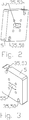
Figure 2 is a schematic isometric front view of an adapter. -
Figure 3 is a schematic isometric back view of the adapter ofFigure 2 . -
Figure 4 is a schematic isometric front view of another adapter. -
Figure 5 is a schematic isometric back view of the adapter ofFigure 4 . -
Figure 6 is a schematic isometric front view of another adapter. -
Figure 7 is a schematic isometric back view of the adapter ofFigure 6 . -
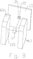
Figure 8 is a schematic exploded isometric view of an adapter, demonstrating interconnections with the adapter seat of a flat panel antenna and two transceivers. -
Figure 9 is a schematic isometric exploded front view of an adapter with a coupling cavity. -
Figure 10 is a schematic isometric exploded back view of the adapter ofFigure 9 . -
Figure 11 is a schematic top view of a layer plate with a top layer overlay, demonstrating symmetrical output port alignment with the coupling cavity. -
Figure 12 is a schematic top view of a layer plate with a top layer overlay, demonstrating asymmetrical output port alignment with the coupling cavity. -
Figure 13 is a schematic top view of a layer plate with a top layer overlay, demonstrating symmetrical output port alignment with the coupling cavity, with a slotted sidewall layer utilizing pins. -
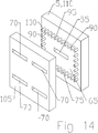
Figure 14 is a schematic isometric exploded front view of an adapter with a slotted sidewall layer utilizing pins. -
Figure 15 is a schematic isometric exploded back view of the adapter ofFigure 14 . -
US Utility Patent Application Serial No. 13/297,304 - The inventors have recognized that prior adapters may be overly complex, overly large and/or require more installation steps than necessary.
- As shown in
Figure 1 , an exemplary embodiment of an adapter includes abase 5 that seats within a recessedadapter seat 10 of anantenna 15 with afeed bore 20. Alternatively, theadapter seat 10 may be provided generally flush and/or protruding from the surface of theantenna 15. Thebase 5 may be retained seated upon and/or within theadapter seat 10, for example, by retaining elements 25 of theadapter seat 10 such as clips 30 dimensioned to engage interlock cavities 35 of thebase 5. The retaining elements 25 may be provided integral with the, for example, machined, die cast or injection molded back side of an input layer of a flat panel-type antenna 15, extending from theadapter seat floor 40 and/oradapter seat sidewall 45. Corresponding interlock cavities 35 provided, for example, as retaining shoulders 50 provided in a periphery of thebase 5 proximate, for example, cross corners of thebase 5 receive and retain thebase 5 in place. - The retention between the
base 5 and theadapter seat 10 may be permanent or releasable via access provided for prying and/or biasing the retaining elements 25 free of engagement with the corresponding interlock cavities 35. Alternatively, the retaining elements 25 may be provided as features of thebase 5 and the interlock cavities 35 provided on theadapter seat 10 and/or conventional fasteners, such as screws or bolts may be applied. Environmental seals (not shown) may be applied, for example, surrounding the feed bore 20 between theadapter seat 10 and thebase 5 and/or around a periphery of thebase 5. - The
base 5 has afeed aperture 55 aligned coaxial with the feed bore 20 when thebase 5 is seated within theadapter seat 10. Thefeed aperture 55 may have the same cross-section as the feed bore 20, provided for example as a generally rectangular, round or square cross-section, for example as shown inFigures 2-7 . - As demonstrated in
Figure 8 , thebase 5 may be provided with a coupler functionality, for example to divide the RF signals between dual signal paths to twotransceivers 60 instead of just one. As shown inFigures 9 and10 , a generallyrectangular coupling cavity 65 may be formed in thebase 5, linking thefeed aperture 55 to two ormore output ports 70. Thefeed aperture 55 and theoutput ports 70 are provided on opposite sides of thecoupling cavity 65. Thecoupling cavity 65 may be dimensioned, for example, with respect to the wavelength of the expected mid-band operating frequency. That is, thecoupling cavity 65 may be provided with dimensions including, for example, a length of 1.5 to 1.7 wavelengths, a width of 0.75 to 1 wavelengths and a depth between thefeed aperture 55 and theoutput ports 70 of approximately 0.2 wavelengths. - The
output ports 70 may be provided with a generally rectangular cross-section, aligned along a length dimension of thecoupling cavity 65 generally parallel to the length of thecoupling cavity 65. As shown inFigures 11 and 12 , theoutput ports 70 may be further aligned offset with respect to thecoupling cavity 65, that is with a midpoint of a width of theoutput port 70 positioned along alength sidewall 75 of thecoupling cavity 65, wherein generally one-half of the output port width is open to thecoupling cavity 65. - Further tuning of the electrical performance of the
coupler cavity 65 may be applied, for example, by including tuning features 80 such as an inward projecting septum 85 provided upon, for example, each of thewidth sidewalls 90 of the coupling cavity, as best demonstrated inFigures 9 and10 . The tuning features 80 may be provided symmetrically with one another on opposing surfaces and/or spaced equidistant between theoutput ports 70. Alternatively, the tuning features 80 may be applied in an asymmetrical configuration. - The level of coupling between the
feed aperture 55 and each of theoutput ports 70 may be selected by, for example, applying theoutput ports 70 aligned symmetrically with a midpoint of thelength sidewall 75 of thecoupling cavity 65, as demonstrated inFigure 11 . Thereby, the coupling between thefeed aperture 55 and each of theoutput ports 70 may configured to be approximately 3 dB. - Alternatively, where the
output ports 70 are positioned aligned asymmetrically with a midpoint of thelength sidewall 75, as demonstrated, for example, inFigure 12 , the coupling between thefeed aperture 55 and each of theoutput ports 70 may be reduced, for example, to approximately 6 or 10 dB, depending upon the level of asymmetrical displacement applied. - In further embodiments, for example as shown in
Figures 13-15 , thecoupling cavity 65 may be configured with an enhanced thermal dissipation and/or thermal isolation characteristic by providingslots 90 open to an exterior of the adapter in the width and/orlength sidewalls 75. Theslots 90 may be, for example, orthogonal, forming sidewall elements withrectangular slots 90 between each. Theslots 90 may be provided with a side-to-side width of, for example, 0.15 to 0.25 wavelengths of a mid-band operating frequency of the adapter. Alternatively, the sidewall elements may be provided ascylindrical pins 95. Thepins 95 may be provided, for example, with a radius of 0.5 wavelengths or less of the mid-band operating frequency of the adapter. To prevent environmental fouling of the signal path, whereslots 90 open to the exterior are applied, a further exterior seal may be applied, such as a polymeric cover or the like. - In alternative embodiments, the coupler configurations described herein above may also be applied in adapter embodiments separate from a recessed adapter seat mating configuration. The
base 5 has been demonstrated as an element with minimal thickness to highlight the space savings possible. Alternatively, the adapter may include an extended feed aperture waveguide, for example extending the position of thecoupler cavity 65 away from theadapter seat 10, closer to inputports 115 of attachedtransceivers 60 for example as shown schematically inFigure 8 . Similarly, abase 5 with afeed aperture 55 configured with a square or circular cross-section (Figures 4-7 ) may extend prior to entering an OMT for division of simultaneous signals of different polarity prior to being routed to attachedtransceivers 60. - One skilled in the art will appreciate that the simplified geometry of the
coupling cavities 65 may enable a significant simplification of the required layer surface features which may reduce overall manufacturing complexity. For example, thebase 5 may be formed cost-effectively with high precision in high volumes via injection molding and/or die-casting technology. One or more separate layers may be applied to arrive at the desired base assembly. For example, as shown inFigures 9 and10 , abase layer 110 may be formed separately from asidewall layer 100 and atop layer 105, which are then stacked upon each other to form thecoupling cavity 65 within the final base assembly. Alternatively, thecoupling cavity 65 may be formed with a recessed portion as the cavity that is then closed by atop layer 105 or thecoupling cavity 65 may be formed as a recessed portion of thetop layer 105 that is closed by thebase layer 110. - Where injection molding with a polymer material is used to form the layers, a conductive surface may be applied.
- Although the coupling cavities and waveguides are described as generally rectangular, for ease of machining and/or mold separation, corners may be radiused and/or rounded and cavity tapers applied in a trade-off between electrical performance and manufacturing efficiency.
- As frequency increases, wavelengths decrease. Therefore, as the desired operating frequency increases, the physical features within the adapter, such as bores, steps, and/or slots become smaller and harder to fabricate. As use of the
coupling cavity 65 can simplify the physical features required, one skilled in the art will appreciate that higher operating frequencies are also enabled by the adapter, for example up to 26 GHz, above which the required dimension resolution/feature precision may begin to make fabrication with acceptable tolerances cost prohibitive. - From the foregoing, it will be apparent that the present invention brings to the art a high performance adapter with reduced overall dimensions that is strong, lightweight and may be repeatedly cost efficiently manufactured with a high level of precision.
Table of Parts 5 base 10 adapter seat 15 antenna 20 feed bore 25 retaining element 30 clip 35 interlock cavity 40 adapter seat floor 45 adapter seat sidewall 50 retaining shoulder 55 feed aperture 60 transceiver 65 coupling cavity 70 output port 75 length sidewall 80 tuning feature 85 septum 90 slot 95 pin 100 sidewall layer 105 top layer 110 base layer 115 input port - Where in the foregoing description reference has been made to materials, ratios, integers or components having known equivalents then such equivalents are herein incorporated as if individually set forth.
- While the present invention has been illustrated by the description of the embodiments thereof, and while the embodiments have been described in considerable detail, it is not the intention of the applicant to restrict or in any way limit the scope of the appended claims to such detail. Additional advantages and modifications will readily appear to those skilled in the art. Therefore, the invention in its broader aspects is not limited to the specific details, representative apparatus, methods, and illustrative examples shown and described.
Claims (9)
- An antenna adapter for an antenna (15), the antenna exhibiting a recessed adapter seat (10) with a feed bore (20), wherein the antenna adapter comprises:a base (5) with a feed aperture (55), anda generally rectangular coupling cavity (65) linking the feed aperture (55) to two generally rectangular output ports (70), wherein the feed aperture (55) and the output ports (70) are provided on opposite sides of the coupling cavity (65); wherein the base (5) is dimensioned to seat within the recessed adapter seat (10), wherein the feed aperture (55) is aligned coaxially with the feed bore (20); wherein the base (5) is provided with interlock cavities (35) dimensioned to receive retaining elements (25) of the recessed adapter seat (10) as the base (5) is inserted into the recessed adapter seat (10), and wherein the retaining elements (25) are configured to engage the interlock cavities (35) to retain the base (5) within the recessed adapter seat (10), andwherein the output ports (70) are generally aligned such that a midpoint of a width of each output port is positioned along a length sidewall of the coupling cavity (65), whereby generally one-half of the width of each output port is open to the coupling cavity (65).
- The antenna adapter of claim 1, wherein the retaining elements (25) are clips (30) and the interlock cavities (35) are retaining shoulders (50) provided in a periphery of the base (5).
- The antenna adapter of claim 1, wherein the coupling cavity (65) is provided with a length of 1.5 to 1.7 wavelengths, a width of 0.75 to 1 wavelengths and a depth between the feed aperture (55) and the output ports (70) of approximately 0.2 wavelengths; the wavelengths being a wavelength of a mid-band operating frequency of the antenna adapter.
- The antenna adapter of claim 1, further including an inwardly projecting septum (85) provided upon at least one sidewall of the coupling cavity (65).
- The antenna adapter of claim 1, wherein each of a width sidewall and a length sidewall of the coupling cavity (65) is provided with slots (90) open to an exterior of the antenna adapter.
- The antenna adapter of claim 5, wherein the slots (90) are generally 0.15 to 0.25 wavelengths, the wavelengths being a wavelength of a mid-band operating frequency of the antenna adapter.
- The antenna adapter of claim 5, wherein the width and length sidewalls are a plurality of cylindrical pins (95).
- The antenna adapter of claim 7, wherein a radius of each pin of the plurality of cylindrical pins (95) is 0.05 wavelengths or less, the wavelengths being a wavelength of a mid-band operating frequency of the antenna adapter.
- The antenna adapter of claim 1, wherein each of a width sidewall and a length sidewall of the coupling cavity (65) is provided with slots (90) open to an exterior of the adapter.
Applications Claiming Priority (3)
| Application Number | Priority Date | Filing Date | Title |
|---|---|---|---|
| US13/297,304 US8558746B2 (en) | 2011-11-16 | 2011-11-16 | Flat panel array antenna |
| US13/677,859 US9160049B2 (en) | 2011-11-16 | 2012-11-15 | Antenna adapter |
| PCT/US2012/065425 WO2013074870A1 (en) | 2011-11-16 | 2012-11-16 | Antenna adapter |
Publications (3)
| Publication Number | Publication Date |
|---|---|
| EP2780978A1 EP2780978A1 (en) | 2014-09-24 |
| EP2780978A4 EP2780978A4 (en) | 2015-07-29 |
| EP2780978B1 true EP2780978B1 (en) | 2021-06-16 |
Family
ID=48280015
Family Applications (1)
| Application Number | Title | Priority Date | Filing Date |
|---|---|---|---|
| EP12849115.6A Active EP2780978B1 (en) | 2011-11-16 | 2012-11-16 | Antenna adapter |
Country Status (8)
| Country | Link |
|---|---|
| US (1) | US9160049B2 (en) |
| EP (1) | EP2780978B1 (en) |
| CN (1) | CN103918123B (en) |
| BR (1) | BR112014011073B1 (en) |
| IN (1) | IN2014DN03443A (en) |
| MX (1) | MX337343B (en) |
| MY (1) | MY167100A (en) |
| WO (1) | WO2013074870A1 (en) |
Family Cites Families (85)
| Publication number | Priority date | Publication date | Assignee | Title |
|---|---|---|---|---|
| US2573746A (en) | 1945-09-19 | 1951-11-06 | Honorary Advisory Council Sci | Directive antenna for microwaves |
| US2862728A (en) | 1955-01-25 | 1958-12-02 | Aircraft Armaments Inc | Detachable coupling device with alignment means |
| US2981948A (en) | 1956-05-29 | 1961-04-25 | Hughes Aircraft Co | Simultaneous lobing array antenna system |
| US3157847A (en) | 1961-07-11 | 1964-11-17 | Robert M Williams | Multilayered waveguide circuitry formed by stacking plates having surface grooves |
| US3243818A (en) | 1962-08-22 | 1966-03-29 | Hughes Aircraft Co | Dual band slot antenna having common waveguide with differing slots, each individualto its own band |
| US3281851A (en) | 1963-05-24 | 1966-10-25 | Hughes Aircraft Co | Dual mode slot antenna |
| US3193830A (en) | 1963-07-25 | 1965-07-06 | Joseph H Provencher | Multifrequency dual ridge waveguide slot antenna |
| US3701162A (en) | 1964-03-24 | 1972-10-24 | Hughes Aircraft Co | Planar antenna array |
| US3340534A (en) | 1965-09-22 | 1967-09-05 | Hughes Aircraft Co | Elliptically or circularly polarized antenna |
| GB1200058A (en) | 1967-04-17 | 1970-07-29 | Elliott Brothers London Ltd | Improvements relating to aerials |
| US3599216A (en) | 1969-08-11 | 1971-08-10 | Nasa | Virtual-wall slot circularly polarized planar array antenna |
| US4121220A (en) | 1975-01-31 | 1978-10-17 | Electronique Marcel Dassault | Flat radar antenna employing circular array of slotted waveguides |
| US4429313A (en) | 1981-11-24 | 1984-01-31 | Muhs Jr Harvey P | Waveguide slot antenna |
| FR2523376A1 (en) | 1982-03-12 | 1983-09-16 | Labo Electronique Physique | RADIATION ELEMENT OR HYPERFREQUENCY SIGNAL RECEIVER WITH LEFT AND RIGHT CIRCULAR POLARIZATIONS AND FLAT ANTENNA COMPRISING A NETWORK OF SUCH JUXTAPOSED ELEMENTS |
| US4949092A (en) | 1984-11-08 | 1990-08-14 | Highes Aircraft Company | Modularized contoured beam direct radiating antenna |
| US4716415A (en) | 1984-12-06 | 1987-12-29 | Kelly Kenneth C | Dual polarization flat plate antenna |
| US5019831A (en) | 1985-05-20 | 1991-05-28 | Texas Instruments Incorporated | Dual end resonant slot array antenna feed having a septum |
| FR2582864B1 (en) * | 1985-06-04 | 1987-07-31 | Labo Electronique Physique | MICROWAVE UNIT MODULES AND MICROWAVE ANTENNA COMPRISING SUCH MODULES |
| FR2592232B1 (en) | 1985-12-20 | 1988-02-12 | Radiotechnique Compelec | MICROWAVE PLANE ANTENNA WITH SUSPENDED SUBSTRATE LINES ARRAY AND METHOD FOR MANUFACTURING THE SAME. |
| US4679011A (en) * | 1986-03-21 | 1987-07-07 | Rca Corporation | Waveguide directional coupler family with a common housing having different sets of conductive block insertable therein |
| US5086304A (en) | 1986-08-13 | 1992-02-04 | Integrated Visual, Inc. | Flat phased array antenna |
| GB8619680D0 (en) | 1986-08-13 | 1986-09-24 | Collins J L F C | Flat plate array |
| US4829309A (en) | 1986-08-14 | 1989-05-09 | Matsushita Electric Works, Ltd. | Planar antenna |
| JPH01103006A (en) | 1987-10-15 | 1989-04-20 | Matsushita Electric Works Ltd | Plane antenna |
| JP2733472B2 (en) | 1988-02-19 | 1998-03-30 | 有限会社ラジアルアンテナ研究所 | Waveguide slot antenna, method of manufacturing the same, and waveguide coupling structure |
| US5210543A (en) | 1988-12-20 | 1993-05-11 | Hughes Aircraft Company | Feed waveguide for an array antenna |
| US5270721A (en) | 1989-05-15 | 1993-12-14 | Matsushita Electric Works, Ltd. | Planar antenna |
| US5321411A (en) | 1990-01-26 | 1994-06-14 | Matsushita Electric Works, Ltd. | Planar antenna for linearly polarized waves |
| US4985708A (en) | 1990-02-08 | 1991-01-15 | Hughes Aircraft Company | Array antenna with slot radiators offset by inclination to eliminate grating lobes |
| US5010351A (en) | 1990-02-08 | 1991-04-23 | Hughes Aircraft Company | Slot radiator assembly with vane tuning |
| FR2669776B1 (en) | 1990-11-23 | 1993-01-22 | Thomson Csf | SLOTTED MICROWAVE ANTENNA WITH LOW THICKNESS STRUCTURE. |
| SE469540B (en) | 1991-11-29 | 1993-07-19 | Ericsson Telefon Ab L M | GUIDANCE GUARANTEE WITH TARGETED HALL ROOM GUARD |
| US5243354A (en) | 1992-08-27 | 1993-09-07 | The United States Of America As Represented By The Secretary Of The Army | Microstrip electronic scan antenna array |
| US5327150A (en) | 1993-03-03 | 1994-07-05 | Hughes Aircraft Company | Phased array antenna for efficient radiation of microwave and thermal energy |
| JPH07106847A (en) | 1993-10-07 | 1995-04-21 | Nippon Steel Corp | Leaky Waveguide Slot Array Antenna |
| SE510082C2 (en) | 1993-11-30 | 1999-04-19 | Saab Ericsson Space Ab | Waveguide antenna with transverse and longitudinal slots |
| US5512906A (en) | 1994-09-12 | 1996-04-30 | Speciale; Ross A. | Clustered phased array antenna |
| US5589843A (en) | 1994-12-28 | 1996-12-31 | Radio Frequency Systems, Inc. | Antenna system with tapered aperture antenna and microstrip phase shifting feed network |
| RU2083035C1 (en) | 1995-06-05 | 1997-06-27 | Александр Данилович Христич | High-frequency planar-array antenna |
| US5650793A (en) | 1995-06-06 | 1997-07-22 | Hughes Missile Systems Company | Centered longitudinal series/series coupling slot for coupling energy between a boxed stripline and a crossed rectangular waveguide and antenna array employing same |
| US5619216A (en) | 1995-06-06 | 1997-04-08 | Hughes Missile Systems Company | Dual polarization common aperture array formed by waveguide-fed, planar slot array and linear short backfire array |
| FI99221C (en) | 1995-08-25 | 1997-10-27 | Nokia Telecommunications Oy | Planar antenna construction |
| GB9703748D0 (en) | 1997-02-22 | 1997-04-09 | Fortel International Limited | Microwave antennas |
| FR2764738B1 (en) | 1997-06-13 | 1999-08-27 | Thomson Csf | INTEGRATED TRANSMISSION OR RECEPTION DEVICE |
| US6028562A (en) | 1997-07-31 | 2000-02-22 | Ems Technologies, Inc. | Dual polarized slotted array antenna |
| US6101705A (en) | 1997-11-18 | 2000-08-15 | Raytheon Company | Methods of fabricating true-time-delay continuous transverse stub array antennas |
| US5880695A (en) | 1998-02-05 | 1999-03-09 | Astron Corporation | Antenna system for wireless comunication systems |
| SE513586C2 (en) | 1998-05-12 | 2000-10-02 | Ericsson Telefon Ab L M | Method of producing an antenna structure and antenna structure prepared by said method |
| US6292142B1 (en) * | 1999-05-24 | 2001-09-18 | Raytheon Company | Locking assembly |
| US7577398B2 (en) | 2000-01-14 | 2009-08-18 | Andrew Llc | Repeaters for wireless communication systems |
| US6201508B1 (en) | 1999-12-13 | 2001-03-13 | Space Systems/Loral, Inc. | Injection-molded phased array antenna system |
| DE60044826D1 (en) | 2000-04-18 | 2010-09-23 | Hitachi Chemical Co Ltd | PLANAR ANTENNA FOR BEAM SCANNING |
| US6304228B1 (en) | 2000-10-06 | 2001-10-16 | Space Systems/Loral, Inc. | Stepped waveguide slot array with phase control and satellite communication system employing same |
| JP4021150B2 (en) | 2001-01-29 | 2007-12-12 | 沖電気工業株式会社 | Slot array antenna |
| EP1371112B1 (en) | 2001-03-21 | 2007-05-02 | Microface Co. Ltd | Waveguide slot antenna and manufacturing method thereof |
| US6476772B1 (en) | 2001-04-16 | 2002-11-05 | Space Systems/Loral, Inc. | Waveguide slot array capable of radiating shaped beams |
| US7680516B2 (en) | 2001-05-02 | 2010-03-16 | Trex Enterprises Corp. | Mobile millimeter wave communication link |
| DE10126468B4 (en) | 2001-05-31 | 2007-07-05 | Eads Deutschland Gmbh | slot antenna |
| US6731241B2 (en) | 2001-06-13 | 2004-05-04 | Raytheon Company | Dual-polarization common aperture antenna with rectangular wave-guide fed centered longitudinal slot array and micro-stripline fed air cavity back transverse series slot array |
| US6624787B2 (en) | 2001-10-01 | 2003-09-23 | Raytheon Company | Slot coupled, polarized, egg-crate radiator |
| JP3928035B2 (en) | 2001-12-27 | 2007-06-13 | 株式会社エッチ・ケー・エス | Turbocharger |
| US6950066B2 (en) | 2002-08-22 | 2005-09-27 | Skycross, Inc. | Apparatus and method for forming a monolithic surface-mountable antenna |
| US6975267B2 (en) | 2003-02-05 | 2005-12-13 | Northrop Grumman Corporation | Low profile active electronically scanned antenna (AESA) for Ka-band radar systems |
| JP4162525B2 (en) | 2003-03-28 | 2008-10-08 | 日本圧着端子製造株式会社 | Connector unit for high frequency radio |
| US6985057B2 (en) | 2003-09-17 | 2006-01-10 | Andrew Corporation | Quick turn-lock waveguide transition assembly |
| US7391381B2 (en) | 2004-01-07 | 2008-06-24 | Motia | Vehicle mounted satellite antenna system with in-motion tracking using beam forming |
| US7227508B2 (en) | 2004-01-07 | 2007-06-05 | Motia Inc. | Vehicle mounted satellite antenna embedded within moonroof or sunroof |
| US6977621B2 (en) | 2004-01-07 | 2005-12-20 | Motia, Inc. | Vehicle mounted satellite antenna system with inverted L-shaped waveguide |
| WO2005079158A2 (en) | 2004-02-23 | 2005-09-01 | Galtronics Ltd. | Conical beam cross-slot antenna |
| US7079087B2 (en) * | 2004-09-27 | 2006-07-18 | Centurion Wireless Technologies, Inc. | Antenna joint connector |
| US7205948B2 (en) | 2005-05-24 | 2007-04-17 | Raytheon Company | Variable inclination array antenna |
| IL174549A (en) | 2005-10-16 | 2010-12-30 | Starling Advanced Comm Ltd | Dual polarization planar array antenna and cell elements therefor |
| TWM292795U (en) | 2005-12-30 | 2006-06-21 | T Conn Prec Corp | Insulation cover structure for antenna connector |
| GB2434923A (en) | 2006-02-03 | 2007-08-08 | Ericsson Telefon Ab L M | Antenna feed device using two separate L-shaped waveguides to give an overall T-shape |
| GB2434922A (en) | 2006-02-03 | 2007-08-08 | Ericsson Telefon Ab L M | Ortho-mode transducer connecting two rectangular waveguides to a common circular waveguide |
| JP4394147B2 (en) | 2006-02-06 | 2010-01-06 | 三菱電機株式会社 | High frequency module |
| USD576344S1 (en) | 2006-08-01 | 2008-09-02 | Lowel-Light Manufacturing, Inc. | Male pin holder for lighting fixture |
| JP5399256B2 (en) | 2006-11-15 | 2014-01-29 | ピルキントン オートモーティヴ ドイチェラント ゲーエムベーハー | Antenna connector |
| KR20080064470A (en) * | 2007-01-05 | 2008-07-09 | 삼성전자주식회사 | Antenna assembly and information processing device having same |
| US7948443B2 (en) | 2008-01-23 | 2011-05-24 | The Boeing Company | Structural feed aperture for space based phased array antennas |
| US7817097B2 (en) | 2008-04-07 | 2010-10-19 | Toyota Motor Engineering & Manufacturing North America, Inc. | Microwave antenna and method for making same |
| US7607942B1 (en) | 2008-08-14 | 2009-10-27 | Andrew Llc | Multi-shot coaxial connector and method of manufacture |
| US8760361B2 (en) | 2009-09-29 | 2014-06-24 | Andrew Llc | Method and apparatus for fine polarization reflector antenna adjustment |
| CN103647154B (en) | 2010-03-12 | 2016-05-25 | 康普技术有限责任公司 | Dual-polarized reflector antenna assembly |
| CN102142619A (en) * | 2011-01-21 | 2011-08-03 | 杭州电子科技大学 | Cavity backed double-slit integrated antenna with increased gain |
-
2012
- 2012-11-15 US US13/677,859 patent/US9160049B2/en active Active
- 2012-11-16 CN CN201280055059.XA patent/CN103918123B/en not_active Expired - Fee Related
- 2012-11-16 MX MX2014005725A patent/MX337343B/en active IP Right Grant
- 2012-11-16 WO PCT/US2012/065425 patent/WO2013074870A1/en not_active Ceased
- 2012-11-16 IN IN3443DEN2014 patent/IN2014DN03443A/en unknown
- 2012-11-16 MY MYPI2014001173A patent/MY167100A/en unknown
- 2012-11-16 EP EP12849115.6A patent/EP2780978B1/en active Active
- 2012-11-16 BR BR112014011073-5A patent/BR112014011073B1/en not_active IP Right Cessation
Non-Patent Citations (1)
| Title |
|---|
| None * |
Also Published As
| Publication number | Publication date |
|---|---|
| WO2013074870A1 (en) | 2013-05-23 |
| US9160049B2 (en) | 2015-10-13 |
| BR112014011073A2 (en) | 2017-06-13 |
| EP2780978A1 (en) | 2014-09-24 |
| MY167100A (en) | 2018-08-10 |
| US20130120089A1 (en) | 2013-05-16 |
| BR112014011073B1 (en) | 2022-01-11 |
| BR112014011073A8 (en) | 2017-12-26 |
| EP2780978A4 (en) | 2015-07-29 |
| MX2014005725A (en) | 2014-05-30 |
| CN103918123B (en) | 2016-08-24 |
| IN2014DN03443A (en) | 2015-06-05 |
| MX337343B (en) | 2016-02-26 |
| CN103918123A (en) | 2014-07-09 |
Similar Documents
| Publication | Publication Date | Title |
|---|---|---|
| EP2780982B1 (en) | Modular feed network | |
| US11095009B2 (en) | Partial dielectric loaded septum polarizer | |
| CN102195141B (en) | Dual Polarized Reflector Antenna Assembly | |
| US8558746B2 (en) | Flat panel array antenna | |
| US10249922B2 (en) | Partial dielectric loaded septum polarizer | |
| US9287605B2 (en) | Passive coaxial power splitter/combiner | |
| EP2494651B1 (en) | Selectable Coupling Level Waveguide Coupler | |
| CN108475852A (en) | Flat plate array antenna with integrated polarization rotating joint | |
| EP1646105A1 (en) | Filter assemblies and communication systems based thereon | |
| CN119965512B (en) | A gap waveguide cavity filter power divider | |
| US9160049B2 (en) | Antenna adapter | |
| EP2345099A1 (en) | A waveguide antenna front end | |
| US12230876B1 (en) | Integrated microwave radio frequency feed network | |
| CN114156624A (en) | Millimeter-wave broadband low-loss directional coupler based on gap waveguide structure | |
| US12592477B2 (en) | Antenna, antenna array and mobile communication base station | |
| TWI460924B (en) | Dual polarized reflector antenna assembly | |
| WO2002075839A1 (en) | Microwave coupler | |
| CN117039382A (en) | Waveguide conversion modules, phased array transceivers and active phased array antennas | |
| CN112532269A (en) | Radio frequency device | |
| Hong | An ultra-wideband transmit/receive module using 10 to 35 GHz six-channel microstrip multiplexers and its applications to phased-array antenna transceiver systems |
Legal Events
| Date | Code | Title | Description |
|---|---|---|---|
| PUAI | Public reference made under article 153(3) epc to a published international application that has entered the european phase |
Free format text: ORIGINAL CODE: 0009012 |
|
| 17P | Request for examination filed |
Effective date: 20140424 |
|
| AK | Designated contracting states |
Kind code of ref document: A1 Designated state(s): AL AT BE BG CH CY CZ DE DK EE ES FI FR GB GR HR HU IE IS IT LI LT LU LV MC MK MT NL NO PL PT RO RS SE SI SK SM TR |
|
| DAX | Request for extension of the european patent (deleted) | ||
| RAP1 | Party data changed (applicant data changed or rights of an application transferred) |
Owner name: COMMSCOPE TECHNOLOGIES LLC |
|
| RA4 | Supplementary search report drawn up and despatched (corrected) |
Effective date: 20150626 |
|
| RIC1 | Information provided on ipc code assigned before grant |
Ipc: H01Q 21/10 20060101AFI20150622BHEP Ipc: H01Q 1/12 20060101ALI20150622BHEP Ipc: H01Q 21/00 20060101ALI20150622BHEP Ipc: H01Q 21/06 20060101ALI20150622BHEP |
|
| STAA | Information on the status of an ep patent application or granted ep patent |
Free format text: STATUS: EXAMINATION IS IN PROGRESS |
|
| 17Q | First examination report despatched |
Effective date: 20171220 |
|
| GRAP | Despatch of communication of intention to grant a patent |
Free format text: ORIGINAL CODE: EPIDOSNIGR1 |
|
| STAA | Information on the status of an ep patent application or granted ep patent |
Free format text: STATUS: GRANT OF PATENT IS INTENDED |
|
| INTG | Intention to grant announced |
Effective date: 20210226 |
|
| GRAS | Grant fee paid |
Free format text: ORIGINAL CODE: EPIDOSNIGR3 |
|
| GRAA | (expected) grant |
Free format text: ORIGINAL CODE: 0009210 |
|
| STAA | Information on the status of an ep patent application or granted ep patent |
Free format text: STATUS: THE PATENT HAS BEEN GRANTED |
|
| AK | Designated contracting states |
Kind code of ref document: B1 Designated state(s): AL AT BE BG CH CY CZ DE DK EE ES FI FR GB GR HR HU IE IS IT LI LT LU LV MC MK MT NL NO PL PT RO RS SE SI SK SM TR |
|
| REG | Reference to a national code |
Ref country code: GB Ref legal event code: FG4D |
|
| REG | Reference to a national code |
Ref country code: CH Ref legal event code: EP |
|
| REG | Reference to a national code |
Ref country code: DE Ref legal event code: R096 Ref document number: 602012075869 Country of ref document: DE |
|
| REG | Reference to a national code |
Ref country code: AT Ref legal event code: REF Ref document number: 1403104 Country of ref document: AT Kind code of ref document: T Effective date: 20210715 |
|
| REG | Reference to a national code |
Ref country code: IE Ref legal event code: FG4D |
|
| REG | Reference to a national code |
Ref country code: SE Ref legal event code: TRGR |
|
| REG | Reference to a national code |
Ref country code: LT Ref legal event code: MG9D |
|
| PG25 | Lapsed in a contracting state [announced via postgrant information from national office to epo] |
Ref country code: BG Free format text: LAPSE BECAUSE OF FAILURE TO SUBMIT A TRANSLATION OF THE DESCRIPTION OR TO PAY THE FEE WITHIN THE PRESCRIBED TIME-LIMIT Effective date: 20210916 Ref country code: HR Free format text: LAPSE BECAUSE OF FAILURE TO SUBMIT A TRANSLATION OF THE DESCRIPTION OR TO PAY THE FEE WITHIN THE PRESCRIBED TIME-LIMIT Effective date: 20210616 Ref country code: LT Free format text: LAPSE BECAUSE OF FAILURE TO SUBMIT A TRANSLATION OF THE DESCRIPTION OR TO PAY THE FEE WITHIN THE PRESCRIBED TIME-LIMIT Effective date: 20210616 Ref country code: FI Free format text: LAPSE BECAUSE OF FAILURE TO SUBMIT A TRANSLATION OF THE DESCRIPTION OR TO PAY THE FEE WITHIN THE PRESCRIBED TIME-LIMIT Effective date: 20210616 |
|
| REG | Reference to a national code |
Ref country code: AT Ref legal event code: MK05 Ref document number: 1403104 Country of ref document: AT Kind code of ref document: T Effective date: 20210616 |
|
| REG | Reference to a national code |
Ref country code: NL Ref legal event code: MP Effective date: 20210616 |
|
| PG25 | Lapsed in a contracting state [announced via postgrant information from national office to epo] |
Ref country code: NO Free format text: LAPSE BECAUSE OF FAILURE TO SUBMIT A TRANSLATION OF THE DESCRIPTION OR TO PAY THE FEE WITHIN THE PRESCRIBED TIME-LIMIT Effective date: 20210916 Ref country code: GR Free format text: LAPSE BECAUSE OF FAILURE TO SUBMIT A TRANSLATION OF THE DESCRIPTION OR TO PAY THE FEE WITHIN THE PRESCRIBED TIME-LIMIT Effective date: 20210917 Ref country code: LV Free format text: LAPSE BECAUSE OF FAILURE TO SUBMIT A TRANSLATION OF THE DESCRIPTION OR TO PAY THE FEE WITHIN THE PRESCRIBED TIME-LIMIT Effective date: 20210616 Ref country code: RS Free format text: LAPSE BECAUSE OF FAILURE TO SUBMIT A TRANSLATION OF THE DESCRIPTION OR TO PAY THE FEE WITHIN THE PRESCRIBED TIME-LIMIT Effective date: 20210616 |
|
| PG25 | Lapsed in a contracting state [announced via postgrant information from national office to epo] |
Ref country code: AT Free format text: LAPSE BECAUSE OF FAILURE TO SUBMIT A TRANSLATION OF THE DESCRIPTION OR TO PAY THE FEE WITHIN THE PRESCRIBED TIME-LIMIT Effective date: 20210616 Ref country code: NL Free format text: LAPSE BECAUSE OF FAILURE TO SUBMIT A TRANSLATION OF THE DESCRIPTION OR TO PAY THE FEE WITHIN THE PRESCRIBED TIME-LIMIT Effective date: 20210616 Ref country code: RO Free format text: LAPSE BECAUSE OF FAILURE TO SUBMIT A TRANSLATION OF THE DESCRIPTION OR TO PAY THE FEE WITHIN THE PRESCRIBED TIME-LIMIT Effective date: 20210616 Ref country code: PT Free format text: LAPSE BECAUSE OF FAILURE TO SUBMIT A TRANSLATION OF THE DESCRIPTION OR TO PAY THE FEE WITHIN THE PRESCRIBED TIME-LIMIT Effective date: 20211018 Ref country code: ES Free format text: LAPSE BECAUSE OF FAILURE TO SUBMIT A TRANSLATION OF THE DESCRIPTION OR TO PAY THE FEE WITHIN THE PRESCRIBED TIME-LIMIT Effective date: 20210616 Ref country code: CZ Free format text: LAPSE BECAUSE OF FAILURE TO SUBMIT A TRANSLATION OF THE DESCRIPTION OR TO PAY THE FEE WITHIN THE PRESCRIBED TIME-LIMIT Effective date: 20210616 Ref country code: EE Free format text: LAPSE BECAUSE OF FAILURE TO SUBMIT A TRANSLATION OF THE DESCRIPTION OR TO PAY THE FEE WITHIN THE PRESCRIBED TIME-LIMIT Effective date: 20210616 Ref country code: SK Free format text: LAPSE BECAUSE OF FAILURE TO SUBMIT A TRANSLATION OF THE DESCRIPTION OR TO PAY THE FEE WITHIN THE PRESCRIBED TIME-LIMIT Effective date: 20210616 Ref country code: SM Free format text: LAPSE BECAUSE OF FAILURE TO SUBMIT A TRANSLATION OF THE DESCRIPTION OR TO PAY THE FEE WITHIN THE PRESCRIBED TIME-LIMIT Effective date: 20210616 |
|
| PG25 | Lapsed in a contracting state [announced via postgrant information from national office to epo] |
Ref country code: PL Free format text: LAPSE BECAUSE OF FAILURE TO SUBMIT A TRANSLATION OF THE DESCRIPTION OR TO PAY THE FEE WITHIN THE PRESCRIBED TIME-LIMIT Effective date: 20210616 |
|
| REG | Reference to a national code |
Ref country code: DE Ref legal event code: R097 Ref document number: 602012075869 Country of ref document: DE |
|
| PLBE | No opposition filed within time limit |
Free format text: ORIGINAL CODE: 0009261 |
|
| STAA | Information on the status of an ep patent application or granted ep patent |
Free format text: STATUS: NO OPPOSITION FILED WITHIN TIME LIMIT |
|
| PG25 | Lapsed in a contracting state [announced via postgrant information from national office to epo] |
Ref country code: DK Free format text: LAPSE BECAUSE OF FAILURE TO SUBMIT A TRANSLATION OF THE DESCRIPTION OR TO PAY THE FEE WITHIN THE PRESCRIBED TIME-LIMIT Effective date: 20210616 |
|
| 26N | No opposition filed |
Effective date: 20220317 |
|
| PG25 | Lapsed in a contracting state [announced via postgrant information from national office to epo] |
Ref country code: AL Free format text: LAPSE BECAUSE OF FAILURE TO SUBMIT A TRANSLATION OF THE DESCRIPTION OR TO PAY THE FEE WITHIN THE PRESCRIBED TIME-LIMIT Effective date: 20210616 |
|
| REG | Reference to a national code |
Ref country code: DE Ref legal event code: R119 Ref document number: 602012075869 Country of ref document: DE |
|
| PG25 | Lapsed in a contracting state [announced via postgrant information from national office to epo] |
Ref country code: MC Free format text: LAPSE BECAUSE OF FAILURE TO SUBMIT A TRANSLATION OF THE DESCRIPTION OR TO PAY THE FEE WITHIN THE PRESCRIBED TIME-LIMIT Effective date: 20210616 |
|
| REG | Reference to a national code |
Ref country code: CH Ref legal event code: PL |
|
| GBPC | Gb: european patent ceased through non-payment of renewal fee |
Effective date: 20211116 |
|
| PG25 | Lapsed in a contracting state [announced via postgrant information from national office to epo] |
Ref country code: LU Free format text: LAPSE BECAUSE OF NON-PAYMENT OF DUE FEES Effective date: 20211116 Ref country code: IT Free format text: LAPSE BECAUSE OF FAILURE TO SUBMIT A TRANSLATION OF THE DESCRIPTION OR TO PAY THE FEE WITHIN THE PRESCRIBED TIME-LIMIT Effective date: 20210616 Ref country code: BE Free format text: LAPSE BECAUSE OF NON-PAYMENT OF DUE FEES Effective date: 20211130 |
|
| REG | Reference to a national code |
Ref country code: BE Ref legal event code: MM Effective date: 20211130 |
|
| PG25 | Lapsed in a contracting state [announced via postgrant information from national office to epo] |
Ref country code: LI Free format text: LAPSE BECAUSE OF NON-PAYMENT OF DUE FEES Effective date: 20211130 Ref country code: CH Free format text: LAPSE BECAUSE OF NON-PAYMENT OF DUE FEES Effective date: 20211130 |
|
| PG25 | Lapsed in a contracting state [announced via postgrant information from national office to epo] |
Ref country code: IE Free format text: LAPSE BECAUSE OF NON-PAYMENT OF DUE FEES Effective date: 20211116 Ref country code: GB Free format text: LAPSE BECAUSE OF NON-PAYMENT OF DUE FEES Effective date: 20211116 Ref country code: DE Free format text: LAPSE BECAUSE OF NON-PAYMENT OF DUE FEES Effective date: 20220601 |
|
| PGFP | Annual fee paid to national office [announced via postgrant information from national office to epo] |
Ref country code: SE Payment date: 20221127 Year of fee payment: 11 Ref country code: FR Payment date: 20221123 Year of fee payment: 11 |
|
| PG25 | Lapsed in a contracting state [announced via postgrant information from national office to epo] |
Ref country code: HU Free format text: LAPSE BECAUSE OF FAILURE TO SUBMIT A TRANSLATION OF THE DESCRIPTION OR TO PAY THE FEE WITHIN THE PRESCRIBED TIME-LIMIT; INVALID AB INITIO Effective date: 20121116 Ref country code: CY Free format text: LAPSE BECAUSE OF FAILURE TO SUBMIT A TRANSLATION OF THE DESCRIPTION OR TO PAY THE FEE WITHIN THE PRESCRIBED TIME-LIMIT Effective date: 20210616 |
|
| P01 | Opt-out of the competence of the unified patent court (upc) registered |
Effective date: 20230530 |
|
| PG25 | Lapsed in a contracting state [announced via postgrant information from national office to epo] |
Ref country code: MK Free format text: LAPSE BECAUSE OF FAILURE TO SUBMIT A TRANSLATION OF THE DESCRIPTION OR TO PAY THE FEE WITHIN THE PRESCRIBED TIME-LIMIT Effective date: 20210616 |
|
| REG | Reference to a national code |
Ref country code: SE Ref legal event code: EUG |
|
| PG25 | Lapsed in a contracting state [announced via postgrant information from national office to epo] |
Ref country code: SE Free format text: LAPSE BECAUSE OF NON-PAYMENT OF DUE FEES Effective date: 20231117 |
|
| PG25 | Lapsed in a contracting state [announced via postgrant information from national office to epo] |
Ref country code: MT Free format text: LAPSE BECAUSE OF FAILURE TO SUBMIT A TRANSLATION OF THE DESCRIPTION OR TO PAY THE FEE WITHIN THE PRESCRIBED TIME-LIMIT Effective date: 20210616 |
|
| PG25 | Lapsed in a contracting state [announced via postgrant information from national office to epo] |
Ref country code: FR Free format text: LAPSE BECAUSE OF NON-PAYMENT OF DUE FEES Effective date: 20231130 |
|
| PG25 | Lapsed in a contracting state [announced via postgrant information from national office to epo] |
Ref country code: FR Free format text: LAPSE BECAUSE OF NON-PAYMENT OF DUE FEES Effective date: 20231130 |
|
| PG25 | Lapsed in a contracting state [announced via postgrant information from national office to epo] |
Ref country code: TR Free format text: LAPSE BECAUSE OF FAILURE TO SUBMIT A TRANSLATION OF THE DESCRIPTION OR TO PAY THE FEE WITHIN THE PRESCRIBED TIME-LIMIT Effective date: 20210616 |