EP2779808A1 - Differential passive equalizer - Google Patents
Differential passive equalizer Download PDFInfo
- Publication number
- EP2779808A1 EP2779808A1 EP14159981.1A EP14159981A EP2779808A1 EP 2779808 A1 EP2779808 A1 EP 2779808A1 EP 14159981 A EP14159981 A EP 14159981A EP 2779808 A1 EP2779808 A1 EP 2779808A1
- Authority
- EP
- European Patent Office
- Prior art keywords
- reference plane
- signal
- circuit board
- spiral inductor
- coupled
- Prior art date
- Legal status (The legal status is an assumption and is not a legal conclusion. Google has not performed a legal analysis and makes no representation as to the accuracy of the status listed.)
- Ceased
Links
Images




Classifications
-
- H—ELECTRICITY
- H05—ELECTRIC TECHNIQUES NOT OTHERWISE PROVIDED FOR
- H05K—PRINTED CIRCUITS; CASINGS OR CONSTRUCTIONAL DETAILS OF ELECTRIC APPARATUS; MANUFACTURE OF ASSEMBLAGES OF ELECTRICAL COMPONENTS
- H05K1/00—Printed circuits
- H05K1/16—Printed circuits incorporating printed electric components, e.g. printed resistors, capacitors or inductors
-
- H—ELECTRICITY
- H01—ELECTRIC ELEMENTS
- H01P—WAVEGUIDES; RESONATORS, LINES, OR OTHER DEVICES OF THE WAVEGUIDE TYPE
- H01P3/00—Waveguides; Transmission lines of the waveguide type
- H01P3/02—Waveguides; Transmission lines of the waveguide type with two longitudinal conductors
- H01P3/08—Microstrips; Strip lines
-
- H—ELECTRICITY
- H04—ELECTRIC COMMUNICATION TECHNIQUE
- H04B—TRANSMISSION
- H04B3/00—Line transmission systems
- H04B3/02—Details
- H04B3/04—Control of transmission; Equalising
- H04B3/14—Control of transmission; Equalising characterised by the equalising network used
-
- H—ELECTRICITY
- H04—ELECTRIC COMMUNICATION TECHNIQUE
- H04L—TRANSMISSION OF DIGITAL INFORMATION, e.g. TELEGRAPHIC COMMUNICATION
- H04L25/00—Baseband systems
- H04L25/02—Details ; arrangements for supplying electrical power along data transmission lines
- H04L25/03—Shaping networks in transmitter or receiver, e.g. adaptive shaping networks
- H04L25/03878—Line equalisers; line build-out devices
-
- H—ELECTRICITY
- H05—ELECTRIC TECHNIQUES NOT OTHERWISE PROVIDED FOR
- H05K—PRINTED CIRCUITS; CASINGS OR CONSTRUCTIONAL DETAILS OF ELECTRIC APPARATUS; MANUFACTURE OF ASSEMBLAGES OF ELECTRICAL COMPONENTS
- H05K1/00—Printed circuits
- H05K1/02—Details
- H05K1/0213—Electrical arrangements not otherwise provided for
- H05K1/0216—Reduction of cross-talk, noise or electromagnetic interference
- H05K1/0218—Reduction of cross-talk, noise or electromagnetic interference by printed shielding conductors, ground planes or power plane
- H05K1/0224—Patterned shielding planes, ground planes or power planes
- H05K1/0225—Single or multiple openings in a shielding, ground or power plane
-
- H—ELECTRICITY
- H05—ELECTRIC TECHNIQUES NOT OTHERWISE PROVIDED FOR
- H05K—PRINTED CIRCUITS; CASINGS OR CONSTRUCTIONAL DETAILS OF ELECTRIC APPARATUS; MANUFACTURE OF ASSEMBLAGES OF ELECTRICAL COMPONENTS
- H05K1/00—Printed circuits
- H05K1/02—Details
- H05K1/0213—Electrical arrangements not otherwise provided for
- H05K1/0216—Reduction of cross-talk, noise or electromagnetic interference
- H05K1/023—Reduction of cross-talk, noise or electromagnetic interference using auxiliary mounted passive components or auxiliary substances
- H05K1/0234—Resistors or by disposing resistive or lossy substances in or near power planes
-
- H—ELECTRICITY
- H05—ELECTRIC TECHNIQUES NOT OTHERWISE PROVIDED FOR
- H05K—PRINTED CIRCUITS; CASINGS OR CONSTRUCTIONAL DETAILS OF ELECTRIC APPARATUS; MANUFACTURE OF ASSEMBLAGES OF ELECTRICAL COMPONENTS
- H05K1/00—Printed circuits
- H05K1/16—Printed circuits incorporating printed electric components, e.g. printed resistors, capacitors or inductors
- H05K1/165—Printed circuits incorporating printed electric components, e.g. printed resistors, capacitors or inductors incorporating printed inductors
-
- H—ELECTRICITY
- H05—ELECTRIC TECHNIQUES NOT OTHERWISE PROVIDED FOR
- H05K—PRINTED CIRCUITS; CASINGS OR CONSTRUCTIONAL DETAILS OF ELECTRIC APPARATUS; MANUFACTURE OF ASSEMBLAGES OF ELECTRICAL COMPONENTS
- H05K3/00—Apparatus or processes for manufacturing printed circuits
- H05K3/10—Apparatus or processes for manufacturing printed circuits in which conductive material is applied to the insulating support in such a manner as to form the desired conductive pattern
-
- H—ELECTRICITY
- H01—ELECTRIC ELEMENTS
- H01P—WAVEGUIDES; RESONATORS, LINES, OR OTHER DEVICES OF THE WAVEGUIDE TYPE
- H01P11/00—Apparatus or processes specially adapted for manufacturing waveguides or resonators, lines, or other devices of the waveguide type
-
- H—ELECTRICITY
- H05—ELECTRIC TECHNIQUES NOT OTHERWISE PROVIDED FOR
- H05K—PRINTED CIRCUITS; CASINGS OR CONSTRUCTIONAL DETAILS OF ELECTRIC APPARATUS; MANUFACTURE OF ASSEMBLAGES OF ELECTRICAL COMPONENTS
- H05K1/00—Printed circuits
- H05K1/02—Details
- H05K1/0213—Electrical arrangements not otherwise provided for
- H05K1/0237—High frequency adaptations
- H05K1/0239—Signal transmission by AC coupling
-
- H—ELECTRICITY
- H05—ELECTRIC TECHNIQUES NOT OTHERWISE PROVIDED FOR
- H05K—PRINTED CIRCUITS; CASINGS OR CONSTRUCTIONAL DETAILS OF ELECTRIC APPARATUS; MANUFACTURE OF ASSEMBLAGES OF ELECTRICAL COMPONENTS
- H05K1/00—Printed circuits
- H05K1/02—Details
- H05K1/0213—Electrical arrangements not otherwise provided for
- H05K1/0237—High frequency adaptations
- H05K1/0245—Lay-out of balanced signal pairs, e.g. differential lines or twisted lines
-
- H—ELECTRICITY
- H05—ELECTRIC TECHNIQUES NOT OTHERWISE PROVIDED FOR
- H05K—PRINTED CIRCUITS; CASINGS OR CONSTRUCTIONAL DETAILS OF ELECTRIC APPARATUS; MANUFACTURE OF ASSEMBLAGES OF ELECTRICAL COMPONENTS
- H05K1/00—Printed circuits
- H05K1/02—Details
- H05K1/0213—Electrical arrangements not otherwise provided for
- H05K1/0237—High frequency adaptations
- H05K1/0246—Termination of transmission lines
-
- H—ELECTRICITY
- H05—ELECTRIC TECHNIQUES NOT OTHERWISE PROVIDED FOR
- H05K—PRINTED CIRCUITS; CASINGS OR CONSTRUCTIONAL DETAILS OF ELECTRIC APPARATUS; MANUFACTURE OF ASSEMBLAGES OF ELECTRICAL COMPONENTS
- H05K1/00—Printed circuits
- H05K1/02—Details
- H05K1/0213—Electrical arrangements not otherwise provided for
- H05K1/0237—High frequency adaptations
- H05K1/025—Impedance arrangements, e.g. impedance matching, reduction of parasitic impedance
-
- H—ELECTRICITY
- H05—ELECTRIC TECHNIQUES NOT OTHERWISE PROVIDED FOR
- H05K—PRINTED CIRCUITS; CASINGS OR CONSTRUCTIONAL DETAILS OF ELECTRIC APPARATUS; MANUFACTURE OF ASSEMBLAGES OF ELECTRICAL COMPONENTS
- H05K2201/00—Indexing scheme relating to printed circuits covered by H05K1/00
- H05K2201/09—Shape and layout
- H05K2201/09209—Shape and layout details of conductors
- H05K2201/0929—Conductive planes
- H05K2201/09309—Core having two or more power planes; Capacitive laminate of two power planes
-
- H—ELECTRICITY
- H05—ELECTRIC TECHNIQUES NOT OTHERWISE PROVIDED FOR
- H05K—PRINTED CIRCUITS; CASINGS OR CONSTRUCTIONAL DETAILS OF ELECTRIC APPARATUS; MANUFACTURE OF ASSEMBLAGES OF ELECTRICAL COMPONENTS
- H05K2201/00—Indexing scheme relating to printed circuits covered by H05K1/00
- H05K2201/09—Shape and layout
- H05K2201/09209—Shape and layout details of conductors
- H05K2201/09654—Shape and layout details of conductors covering at least two types of conductors provided for in H05K2201/09218 - H05K2201/095
- H05K2201/0969—Apertured conductors
-
- H—ELECTRICITY
- H05—ELECTRIC TECHNIQUES NOT OTHERWISE PROVIDED FOR
- H05K—PRINTED CIRCUITS; CASINGS OR CONSTRUCTIONAL DETAILS OF ELECTRIC APPARATUS; MANUFACTURE OF ASSEMBLAGES OF ELECTRICAL COMPONENTS
- H05K2201/00—Indexing scheme relating to printed circuits covered by H05K1/00
- H05K2201/10—Details of components or other objects attached to or integrated in a printed circuit board
- H05K2201/10007—Types of components
- H05K2201/10015—Non-printed capacitor
-
- H—ELECTRICITY
- H05—ELECTRIC TECHNIQUES NOT OTHERWISE PROVIDED FOR
- H05K—PRINTED CIRCUITS; CASINGS OR CONSTRUCTIONAL DETAILS OF ELECTRIC APPARATUS; MANUFACTURE OF ASSEMBLAGES OF ELECTRICAL COMPONENTS
- H05K2201/00—Indexing scheme relating to printed circuits covered by H05K1/00
- H05K2201/10—Details of components or other objects attached to or integrated in a printed circuit board
- H05K2201/10007—Types of components
- H05K2201/10022—Non-printed resistor
-
- Y—GENERAL TAGGING OF NEW TECHNOLOGICAL DEVELOPMENTS; GENERAL TAGGING OF CROSS-SECTIONAL TECHNOLOGIES SPANNING OVER SEVERAL SECTIONS OF THE IPC; TECHNICAL SUBJECTS COVERED BY FORMER USPC CROSS-REFERENCE ART COLLECTIONS [XRACs] AND DIGESTS
- Y10—TECHNICAL SUBJECTS COVERED BY FORMER USPC
- Y10T—TECHNICAL SUBJECTS COVERED BY FORMER US CLASSIFICATION
- Y10T29/00—Metal working
- Y10T29/49—Method of mechanical manufacture
- Y10T29/49002—Electrical device making
- Y10T29/49117—Conductor or circuit manufacturing
- Y10T29/49124—On flat or curved insulated base, e.g., printed circuit, etc.
- Y10T29/49155—Manufacturing circuit on or in base
Definitions
- Transmission of electrical signals in a circuit board can result in energy loss.
- the energy loss is usually dependent on the frequency of the transmission. For example, signal loss will generally be higher at higher frequencies.
- the signal loss variation across the frequency range of a signal can make it more difficult for signal receivers to recover the transmitted data.
- signal equalization techniques are used to equalize the frequency dependent loss. These techniques use active circuit designs that consume power. In some cases, a redriver or repeater is needed for extra equalization, requiring additional power.
- a circuit in a transmission system can use passive equalization to correct the frequency dependent loss.
- This passive equalization solution can be less expensive and less power-consuming than present active equalization solutions.
- a circuit board configured for passive equalization includes a spiral structure combined with a defected ground structure to introduce inductance to a transmission signal traveling throughout the circuit board.
- Fig. 1 is a block diagram of a transmission circuit.
- a transmission signal can be sent from a transmitter 102 to a receiver 104.
- the transmission system 100 can include a capacitive coupler 106 and an equalizer 108.
- the transmission circuit 100 can be used in any sort of alternating current (AC) coupled input/output design, such as Peripheral Component Interconnect Express (PCIe), Universal Serial Bus (USB), Serial Advanced Technology Attachment (SATA), Serial Attached Small Computer System Interface (SAS), Direct Media Interface (DMI), QuickPath Interconnect (QPI), Serial Management Interface (SMI), and KG-84 Trunk Interface (KTI), among others.
- PCIe Peripheral Component Interconnect Express
- USB Universal Serial Bus
- SAS Serial Advanced Technology Attachment
- SAS Serial Attached Small Computer System Interface
- DMI Direct Media Interface
- QPI QuickPath Interconnect
- SMI Serial Management Interface
- KTI Serial Management Interface
- the transmission circuit 100 can be analog or digital.
- the capacitive coupler 106 can be used in the transmission circuit 100 to direct current (DC) bias in the transmission signal such that only alternating current (AC) passes through.
- the equalizer 108 can help correct the frequency dependent loss of the transmission signal such that the amount of energy lost from the transmission signal is over a frequency range of interest.
- the equalizer 108 can be passive.
- the transmitter 102, the receiver 104, the capacitive coupler 106, and the equalizer 108 are contained on a single circuit board.
- the transmitter 102 can be contained on a separate circuit board from the receiver 104, the capacitive coupler 106, and the equalizer 108.
- Fig. 2 is a cross section side view of a circuit board, in accordance with embodiments.
- the circuit board 200 can include a first reference plane 202 and a second reference plane 204.
- a transmission signal can enter the circuit board 200 through a signal trace 208 mounted above the first reference plane 202.
- the signal trace 206 is coupled to a signal via 210.
- the transmission signal can exit from the circuit board 200 through an exit trace 214 coupled to the signal via 210.
- the reference planes 202 and 204 can be planar substrates composed of a conductive material that can act as ground in the circuit board 200.
- the signal trace 208, the signal via 210, and the exit trace 214 may be separated from the reference planes 202 and 204 by an insulating layer.
- the circuit board 200 includes a spiral inductor 216 coupled to the signal via 210.
- the spiral inductor 216 can introduce inductance to the signal via 210.
- the spiral inductor 216 can be within proximity of the second reference plane 204. It is to be noted that the spiral inductor 216 is not in direct contact with the second reference plane 204.
- the spiral inductor 216 can be isolated from the second reference plane 204 by an insulating layer.
- the spiral inductor 216 forms a shunt current path that branches from the path of the transmission signal, as illustrated by arrow path 218.
- the magnitude of the signal loss caused by the current shunt path can be inversely proportional to frequency of the transmission signal.
- the inductance value of the spiral inductor 216 can be variable in some embodiments.
- the circuit board 200 can also include a termination resistor 220 coupled to the spiral inductor 216 and a ground via 222 that is coupled to the reference plans 202 and 204.
- the termination resistor 220 is configured to couple the spiral inductor 216 to ground.
- the resistance value of the termination resistors 220 can be variable.
- the second reference plane 204 can include a defected ground structure over which the spiral inductor 216 can reside.
- the defected ground structure can improve the effectiveness of the spiral inductor.
- the circuit board 200 can include a DC blocking capacitor 224 coupled to the signal trace 208.
- the DC blocking capacitor 224 can operate as a capacitive coupler and block direct current in the transmission signal.
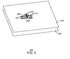
- Fig. 3 is a top perspective view of the circuit board, in accordance with embodiments.
- the signal trace 208 is disposed above the first reference plane 202 and coupled to the signal via 210.
- the DC blocking capacitor 224 can be coupled to the signal trace 208 such that the transmission signal passes through the DC blocking capacitor 224.
- the signal via 210 can be isolated from the first reference plane 202 by empty space or insulating layer.
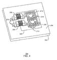
- Fig. 4 is a bottom perspective view of the circuit board, in accordance with embodiments.
- the second reference plane 204 contains a defected ground structure 226 adjacent to which the spiral inductor 216 resides.
- the defected ground structure 226 can be a hole, opening, or etch in the second reference plane 204 that can improve the effectiveness of the spiral inductor 216.
- the defected ground structure 226 can be rectangular, circular, in the shape of the spiral inductor 216, or have any other geometry.
- the spiral inductor 216 may contain a varying number of turns.
- Figs. 5A and 5B are frequency response plots illustrating the performance of passive equalization circuits.
- Plots 500 and 502 illustrate the curve of a transmission signal's insertion loss (represented on the vertical axis, wherein a higher absolute value indicates a higher amount of loss) as a function of the transmission signal's frequency (represented on the horizontal axis).
- the insertion loss is shown to have an upward trend in a range between a minimum equalization frequency 504 and a peak equalization frequency 506.
- the minimum equalization frequency 504 represents the frequency in which only direct current is lost
- the peak equalization frequency 506 represents the frequency in which the highest magnitude of signal is lost.
- the type and geometry of the spiral inductor can affect the range, the peak equalization frequency 506, and the range of insertion loss (or equalization strength).
- the range, the peak equalization frequency 506, and the equalization strength can also be affected by the termination resistance.
- the termination resistance is 30 Ohms, and the peak equalization frequency 506 is approximately 3.7 GHz.
- the termination resistance is 20 Ohms, and the peak equalization frequency 506 is approximately 3.5 GHz.
- Fig. 6 is a process flow diagram of a method of manufacturing a circuit board, in accordance with embodiments.
- the method 600 is used to manufacture a circuit board used for passive equalization in a transmission system.
- a signal trace is disposed above a first reference plane.
- a defected ground structure is etched in a second reference plane.
- a spiral inductor is positioned adjacent to the defected ground structure.
- a signal via is coupled to the signal trace and the spiral inductor.
- a ground via can be connected to the first and second reference planes, and coupled to the spiral inductor.
- a termination resistor can also be disposed on the second reference plane and coupled to the ground via and the spiral inductor.
- An exit trace can be coupled to the signal via.
- a DC blocking capacitor can be coupled to the signal trace and disposed on the first reference plane.
- the circuit board includes a first reference plane and a second reference plane, wherein the second reference plane includes a defected ground structure.
- the circuit board includes a signal trace coupled to a signal via, wherein the signal trace is disposed above the first reference plane.
- the circuit board includes a spiral inductor positioned adjacent to the defected ground structure, wherein the spiral inductor is coupled to the signal via.
- the circuit board may include a ground via connecting the first reference plane and the second reference plane.
- the ground via may be coupled to the spiral inductor.
- the circuit board may include a termination resistor disposed on the second reference plane, wherein the termination resistor is coupled to the spiral inductor and to the ground via.
- the circuit board may include an exit trace coupled to the signal via.
- the circuit board may include a direct current (DC) blocking capacitor coupled to the signal trace, wherein the DC blocking capacitor is disposed on the first reference plane.
- the circuit board may include an insulating layer between the signal trace and the first reference plane.
- the signal trace may be used to transmit a Peripheral Component Interconnect Express (PCIe) signal.
- PCIe Peripheral Component Interconnect Express
- the signal trace may be used to transmit a Universal Serial Bus (USB) signal.
- the signal trace may be used to transmit a Serial Advanced Technology Advancement (SATA) signal or a Serial Attached Small Computer System Interface (SAS) signal.
- SATA Serial Advanced Technology Advancement
- SAS Serial Attached Small Computer System Interface
- the signal trace may be used to transmit a Direct Media Interface (DMI) signal, a QuickPath Interconnect (QPI) signal, a Serial Management Interface (SMI) signal, or a KG-84 Trunk Interface (KTI) signal.
- DMI Direct Media Interface
- QPI QuickPath Interconnect
- SMI Serial Management Interface
- KTI KG-84 Trunk Interface
- the electronic device includes a circuit board.
- the circuit board includes a first reference plane and a second reference plane, wherein the second reference plane includes a defected ground structure.
- the circuit board includes a signal trace coupled to a signal via, wherein the signal trace is disposed above the first reference plane.
- the circuit board includes a spiral inductor positioned adjacent to the defected ground structure, wherein the spiral inductor is coupled to the signal via.
- the circuit board may include a ground via connecting the first reference plane and the second reference plane.
- the ground via may be coupled to the spiral inductor.
- the circuit board may include a termination resistor disposed on the second reference plane, wherein the termination resistor is coupled to the spiral inductor and to the ground via.
- the circuit board may include an exit trace coupled to the signal via.
- the circuit board may include a direct current (DC) blocking capacitor coupled to the signal trace, wherein the DC blocking capacitor is disposed on the first reference plane.
- the circuit board may include an insulating layer between the signal trace and the first reference plane.
- the signal trace may be used to transmit a Peripheral Component Interconnect Express (PCIe) signal.
- PCIe Peripheral Component Interconnect Express
- the signal trace may be used to transmit a Universal Serial Bus (USB) signal.
- the signal trace may be used to transmit a Serial Advanced Technology Advancement (SATA) signal or a Serial Attached Small Computer System Interface (SAS) signal.
- SATA Serial Advanced Technology Advancement
- SAS Serial Attached Small Computer System Interface
- the signal trace may be used to transmit a Direct Media Interface (DMI) signal, a QuickPath Interconnect (QPI) signal, a Serial Management Interface (SMI) signal, or a KG-84 Trunk Interface (KTI) signal.
- DMI Direct Media Interface
- QPI QuickPath Interconnect
- SMI Serial Management Interface
- KTI KG-84 Trunk Interface
- a method of manufacturing a circuit board includes disposing a signal trace above a first reference plane.
- the method includes etching a defected ground structure in a second reference plane.
- the method includes positioning a spiral inductor adjacent to the defected ground structure.
- the method includes coupling a signal via to the signal trace and the spiral inductor.
- the method may include connecting a ground via to the first reference plane and the second reference plane.
- the method may include coupling the spiral inductor to the ground via.
- the method may include disposing a termination resistor on the second reference plane, coupling the termination resistor to the spiral inductor, and coupling the termination resistor to the ground via.
- the method may include coupling an exit trace to the signal via.
- the method may include disposing a DC blocking capacitor on the first reference plane, and coupling the DC blocking capacitor to the signal trace.
- the signal trace may be used to transmit a Peripheral Component Interconnect Express (PCIe) signal.
- PCIe Peripheral Component Interconnect Express
- the signal trace may be used to transmit a Universal Serial Bus (USB) signal.
- the signal trace may be used to transmit a Serial Advanced Technology Advancement (SATA) signal or a Serial Attached Small Computer System Interface (SAS) signal.
- the signal trace may be used to transmit a Direct Media Interface (DMI) signal, a QuickPath Interconnect (QPI) signal, a Serial Management Interface (SMI) signal, or a KG-84 Trunk Interface (KTI) signal.
- DMI Direct Media Interface
- QPI QuickPath Interconnect
- SMI Serial Management Interface
- KTI KG-84 Trunk Interface
- the elements in some cases may each have a same reference number or a different reference number to suggest that the elements represented could be different or similar.
- an element may be flexible enough to have different implementations and work with some or all of the systems shown or described herein.
- the various elements shown in the figures may be the same or different. Which one is referred to as a first element and which is called a second element is arbitrary.
- Coupled may mean that two or more elements are in direct physical or electrical contact. However, “coupled” may also mean that two or more elements are not in direct contact with each other, but yet still co-operate or interact with each other.
- An embodiment is an implementation or example of the inventions.
- Reference in the specification to "an embodiment,” “one embodiment,” “some embodiments,” or “other embodiments” means that a particular feature, structure, or characteristic described in connection with the embodiments is included in at least some embodiments, but not necessarily all embodiments, of the inventions.
- the various appearances “an embodiment,” “one embodiment,” or “some embodiments” are not necessarily all referring to the same embodiments.
Landscapes
- Engineering & Computer Science (AREA)
- Microelectronics & Electronic Packaging (AREA)
- Computer Networks & Wireless Communication (AREA)
- Signal Processing (AREA)
- Physics & Mathematics (AREA)
- Electromagnetism (AREA)
- Power Engineering (AREA)
- Manufacturing & Machinery (AREA)
- Structure Of Printed Boards (AREA)
- Filters And Equalizers (AREA)
Abstract
Description
- Transmission of electrical signals in a circuit board can result in energy loss. The energy loss is usually dependent on the frequency of the transmission. For example, signal loss will generally be higher at higher frequencies. The signal loss variation across the frequency range of a signal can make it more difficult for signal receivers to recover the transmitted data. Accordingly, signal equalization techniques are used to equalize the frequency dependent loss. These techniques use active circuit designs that consume power. In some cases, a redriver or repeater is needed for extra equalization, requiring additional power.
- The following detailed description may be better understood by referencing the accompanying drawings, which contain specific examples of numerous objects and features of the disclosed subject matter.
-
Fig. 1 is a block diagram of a transmission system. -
Fig. 2 is a cross-section side view of the circuit board, in accordance with embodiments. -
Fig. 3 is a top perspective view of the circuit board, in accordance with embodiments. -
Fig. 4 is a bottom perspective view of the circuit board, in accordance with embodiments. -
Figs. 5A and5B are frequency response plots illustrating the performance of passive equalization circuits. -
Fig. 6 is a process flow diagram of a method of manufacturing a circuit board, in accordance with embodiments. - The present disclosure relates to a passive equalization technique for correcting frequency dependent loss in an AC-coupled link. In accordance with embodiments, a circuit in a transmission system can use passive equalization to correct the frequency dependent loss. This passive equalization solution can be less expensive and less power-consuming than present active equalization solutions. In accordance with embodiments, a circuit board configured for passive equalization includes a spiral structure combined with a defected ground structure to introduce inductance to a transmission signal traveling throughout the circuit board.
-
Fig. 1 is a block diagram of a transmission circuit. A transmission signal can be sent from atransmitter 102 to areceiver 104. Thetransmission system 100 can include acapacitive coupler 106 and anequalizer 108. Thetransmission circuit 100 can be used in any sort of alternating current (AC) coupled input/output design, such as Peripheral Component Interconnect Express (PCIe), Universal Serial Bus (USB), Serial Advanced Technology Attachment (SATA), Serial Attached Small Computer System Interface (SAS), Direct Media Interface (DMI), QuickPath Interconnect (QPI), Serial Management Interface (SMI), and KG-84 Trunk Interface (KTI), among others. Thetransmission circuit 100 can be analog or digital. The transmission signal can be differential or single-ended. - The
capacitive coupler 106 can be used in thetransmission circuit 100 to direct current (DC) bias in the transmission signal such that only alternating current (AC) passes through. Theequalizer 108 can help correct the frequency dependent loss of the transmission signal such that the amount of energy lost from the transmission signal is over a frequency range of interest. Theequalizer 108 can be passive. In some embodiments, thetransmitter 102, thereceiver 104, thecapacitive coupler 106, and theequalizer 108 are contained on a single circuit board. In some embodiments, thetransmitter 102 can be contained on a separate circuit board from thereceiver 104, thecapacitive coupler 106, and theequalizer 108. -
Fig. 2 is a cross section side view of a circuit board, in accordance with embodiments. Thecircuit board 200 can include afirst reference plane 202 and asecond reference plane 204. As shown byarrow path 206, a transmission signal can enter thecircuit board 200 through asignal trace 208 mounted above thefirst reference plane 202. Thesignal trace 206 is coupled to a signal via 210. As illustrated in thearrow path 212, the transmission signal can exit from thecircuit board 200 through anexit trace 214 coupled to the signal via 210. - The
reference planes circuit board 200. In order to prevent the transmission signal from shorting out, thesignal trace 208, the signal via 210, and theexit trace 214 may be separated from thereference planes - The
circuit board 200 includes aspiral inductor 216 coupled to the signal via 210. Thespiral inductor 216 can introduce inductance to the signal via 210. Thespiral inductor 216 can be within proximity of thesecond reference plane 204. It is to be noted that thespiral inductor 216 is not in direct contact with thesecond reference plane 204. Thespiral inductor 216 can be isolated from thesecond reference plane 204 by an insulating layer. - The
spiral inductor 216 forms a shunt current path that branches from the path of the transmission signal, as illustrated byarrow path 218. The magnitude of the signal loss caused by the current shunt path can be inversely proportional to frequency of the transmission signal. The inductance value of thespiral inductor 216 can be variable in some embodiments. - In some embodiments, the
circuit board 200 can also include atermination resistor 220 coupled to thespiral inductor 216 and a ground via 222 that is coupled to thereference plans termination resistor 220 is configured to couple thespiral inductor 216 to ground. The resistance value of thetermination resistors 220 can be variable. - The
second reference plane 204 can include a defected ground structure over which thespiral inductor 216 can reside. The defected ground structure can improve the effectiveness of the spiral inductor. - In some embodiments, the
circuit board 200 can include aDC blocking capacitor 224 coupled to thesignal trace 208. TheDC blocking capacitor 224 can operate as a capacitive coupler and block direct current in the transmission signal. -
Fig. 3 is a top perspective view of the circuit board, in accordance with embodiments. As seen inFig. 3 , thesignal trace 208 is disposed above thefirst reference plane 202 and coupled to the signal via 210. TheDC blocking capacitor 224 can be coupled to thesignal trace 208 such that the transmission signal passes through theDC blocking capacitor 224. The signal via 210 can be isolated from thefirst reference plane 202 by empty space or insulating layer. -
Fig. 4 is a bottom perspective view of the circuit board, in accordance with embodiments. As seen inFig. 4 , thesecond reference plane 204 contains a defectedground structure 226 adjacent to which thespiral inductor 216 resides. The defectedground structure 226 can be a hole, opening, or etch in thesecond reference plane 204 that can improve the effectiveness of thespiral inductor 216. The defectedground structure 226 can be rectangular, circular, in the shape of thespiral inductor 216, or have any other geometry. Furthermore, thespiral inductor 216 may contain a varying number of turns. -
Figs. 5A and5B are frequency response plots illustrating the performance of passive equalization circuits.Plots Figs. 5A and5B , the insertion loss is shown to have an upward trend in a range between aminimum equalization frequency 504 and apeak equalization frequency 506. Theminimum equalization frequency 504 represents the frequency in which only direct current is lost, and thepeak equalization frequency 506 represents the frequency in which the highest magnitude of signal is lost. In this range, the amount of data lost from the transmission signal is lessened at higher frequencies. This trend can be the opposite of that which occurs in a wire without equalization, where a higher frequency can result in higher loss of data. Installing the passive equalization circuit into the wire may cause the level of insertion loss to remain relatively stable and independent of frequency. - It is to be noted that the type and geometry of the spiral inductor can affect the range, the
peak equalization frequency 506, and the range of insertion loss (or equalization strength). The range, thepeak equalization frequency 506, and the equalization strength can also be affected by the termination resistance. In theplot 500, the termination resistance is 30 Ohms, and thepeak equalization frequency 506 is approximately 3.7 GHz. In theplot 502, the termination resistance is 20 Ohms, and thepeak equalization frequency 506 is approximately 3.5 GHz. -
Fig. 6 is a process flow diagram of a method of manufacturing a circuit board, in accordance with embodiments. Themethod 600 is used to manufacture a circuit board used for passive equalization in a transmission system. Atblock 602, a signal trace is disposed above a first reference plane. Atblock 604, a defected ground structure is etched in a second reference plane. Atblock 606, a spiral inductor is positioned adjacent to the defected ground structure. Atblock 608, a signal via is coupled to the signal trace and the spiral inductor. - Additionally, a ground via can be connected to the first and second reference planes, and coupled to the spiral inductor. A termination resistor can also be disposed on the second reference plane and coupled to the ground via and the spiral inductor. An exit trace can be coupled to the signal via. In some embodiments, a DC blocking capacitor can be coupled to the signal trace and disposed on the first reference plane.
- A circuit board for passive equalization is described herein. The circuit board includes a first reference plane and a second reference plane, wherein the second reference plane includes a defected ground structure. The circuit board includes a signal trace coupled to a signal via, wherein the signal trace is disposed above the first reference plane. The circuit board includes a spiral inductor positioned adjacent to the defected ground structure, wherein the spiral inductor is coupled to the signal via.
- The circuit board may include a ground via connecting the first reference plane and the second reference plane. The ground via may be coupled to the spiral inductor. The circuit board may include a termination resistor disposed on the second reference plane, wherein the termination resistor is coupled to the spiral inductor and to the ground via. The circuit board may include an exit trace coupled to the signal via. The circuit board may include a direct current (DC) blocking capacitor coupled to the signal trace, wherein the DC blocking capacitor is disposed on the first reference plane. The circuit board may include an insulating layer between the signal trace and the first reference plane.
- The signal trace may be used to transmit a Peripheral Component Interconnect Express (PCIe) signal. The signal trace may be used to transmit a Universal Serial Bus (USB) signal. The signal trace may be used to transmit a Serial Advanced Technology Advancement (SATA) signal or a Serial Attached Small Computer System Interface (SAS) signal. The signal trace may be used to transmit a Direct Media Interface (DMI) signal, a QuickPath Interconnect (QPI) signal, a Serial Management Interface (SMI) signal, or a KG-84 Trunk Interface (KTI) signal.
- An electronic device for passive equalization is described herein. The electronic device includes a circuit board. The circuit board includes a first reference plane and a second reference plane, wherein the second reference plane includes a defected ground structure. The circuit board includes a signal trace coupled to a signal via, wherein the signal trace is disposed above the first reference plane. The circuit board includes a spiral inductor positioned adjacent to the defected ground structure, wherein the spiral inductor is coupled to the signal via.
- The circuit board may include a ground via connecting the first reference plane and the second reference plane. The ground via may be coupled to the spiral inductor. The circuit board may include a termination resistor disposed on the second reference plane, wherein the termination resistor is coupled to the spiral inductor and to the ground via. The circuit board may include an exit trace coupled to the signal via. The circuit board may include a direct current (DC) blocking capacitor coupled to the signal trace, wherein the DC blocking capacitor is disposed on the first reference plane. The circuit board may include an insulating layer between the signal trace and the first reference plane.
- The signal trace may be used to transmit a Peripheral Component Interconnect Express (PCIe) signal. The signal trace may be used to transmit a Universal Serial Bus (USB) signal. The signal trace may be used to transmit a Serial Advanced Technology Advancement (SATA) signal or a Serial Attached Small Computer System Interface (SAS) signal. The signal trace may be used to transmit a Direct Media Interface (DMI) signal, a QuickPath Interconnect (QPI) signal, a Serial Management Interface (SMI) signal, or a KG-84 Trunk Interface (KTI) signal.
- A method of manufacturing a circuit board is described herein. The method includes disposing a signal trace above a first reference plane. The method includes etching a defected ground structure in a second reference plane. The method includes positioning a spiral inductor adjacent to the defected ground structure. The method includes coupling a signal via to the signal trace and the spiral inductor.
- The method may include connecting a ground via to the first reference plane and the second reference plane. The method may include coupling the spiral inductor to the ground via. The method may include disposing a termination resistor on the second reference plane, coupling the termination resistor to the spiral inductor, and coupling the termination resistor to the ground via. The method may include coupling an exit trace to the signal via. The method may include disposing a DC blocking capacitor on the first reference plane, and coupling the DC blocking capacitor to the signal trace. The signal trace may be used to transmit a Peripheral Component Interconnect Express (PCIe) signal.
- The signal trace may be used to transmit a Universal Serial Bus (USB) signal. The signal trace may be used to transmit a Serial Advanced Technology Advancement (SATA) signal or a Serial Attached Small Computer System Interface (SAS) signal. The signal trace may be used to transmit a Direct Media Interface (DMI) signal, a QuickPath Interconnect (QPI) signal, a Serial Management Interface (SMI) signal, or a KG-84 Trunk Interface (KTI) signal.
- Although some embodiments have been described in reference to particular implementations, other implementations are possible according to some embodiments. Additionally, the arrangement and order of circuit elements or other features illustrated in the drawings or described herein need not be arranged in the particular way illustrated and described. Many other arrangements are possible according to some embodiments.
- In each system shown in a figure, the elements in some cases may each have a same reference number or a different reference number to suggest that the elements represented could be different or similar. However, an element may be flexible enough to have different implementations and work with some or all of the systems shown or described herein. The various elements shown in the figures may be the same or different. Which one is referred to as a first element and which is called a second element is arbitrary.
- In the description and claims, the terms "coupled" and "connected," along with their derivatives, may be used. It should be understood that these terms are not intended as synonyms for each other. Rather, in particular embodiments, "connected" may be used to indicate that two or more elements are in direct physical or electrical contact with each other. "Coupled" may mean that two or more elements are in direct physical or electrical contact. However, "coupled" may also mean that two or more elements are not in direct contact with each other, but yet still co-operate or interact with each other.
- An embodiment is an implementation or example of the inventions. Reference in the specification to "an embodiment," "one embodiment," "some embodiments," or "other embodiments" means that a particular feature, structure, or characteristic described in connection with the embodiments is included in at least some embodiments, but not necessarily all embodiments, of the inventions. The various appearances "an embodiment," "one embodiment," or "some embodiments" are not necessarily all referring to the same embodiments.
- Not all components, features, structures, characteristics, etc. described and illustrated herein need be included in a particular embodiment or embodiments. If the specification states a component, feature, structure, or characteristic "may", "might", "can" or "could" be included, for example, that particular component, feature, structure, or characteristic is not required to be included. If the specification or claim refers to "a" or "an" element, that does not mean there is only one of the element. If the specification or claims refer to "an additional" element, that does not preclude there being more than one of the additional element.
- Although flow diagrams and state diagrams may have been used herein to describe embodiments, the inventions are not limited to those diagrams or to corresponding descriptions herein. For example, flow need not move through each illustrated box or state or in exactly the same order as illustrated and described herein.
- The inventions are not restricted to the particular details listed herein. Indeed, those skilled in the art having the benefit of this disclosure will appreciate that many other variations from the foregoing description and drawings may be made within the scope of the present inventions. Accordingly, it is the following claims including any amendments thereto that define the scope of the inventions.
Claims (15)
- A circuit board, comprising:a first reference plane and a second reference plane, the second reference plane comprising a defected ground structure;a signal trace coupled to a signal via, the signal trace disposed above the first reference plane; anda spiral inductor positioned adjacent to the defected ground structure, the spiral inductor coupled to the signal via.
- The circuit board of claim 1, comprising a ground via connecting the first reference plane and the second reference plane.
- The circuit board of claim 2, the ground via coupled to the spiral inductor.
- The circuit board of claim 3, comprising a termination resistor disposed on the second reference plane, the termination resistor coupled to the spiral inductor and to the ground via.
- The circuit board of claim 1, comprising an exit trace coupled to the signal via.
- The circuit board of claim 1, comprising a direct current (DC) blocking capacitor coupled to the signal trace, the DC blocking capacitor disposed on the first reference plane.
- An electronic device, comprising:a circuit board comprising:a first reference plane and a second reference plane, the second reference plane comprising a defected ground structure;a signal trace coupled to a signal via, the signal trace disposed above the first reference plane; anda spiral inductor positioned adjacent to the defected ground structure, the spiral inductor coupled to the signal via.
- The electronic device of claim 7, the circuit board comprising a ground via connecting the first reference plane and the second reference plane.
- The electronic device of claim 8, the ground via coupled to the spiral inductor.
- A method of manufacturing a circuit board, comprising:disposing a signal trace above a first reference plane;etching a defected ground structure in a second reference plane;positioning a spiral inductor adjacent to the defected ground structure; andcoupling a signal via to the signal trace and the spiral inductor.
- The method of claim 10, comprising connecting a ground via to the first reference plane and the second reference plane.
- The method of claim 11, comprising coupling the spiral inductor to the ground via.
- The method of claim 12, comprising:disposing a termination resistor on the second reference plane;coupling the termination resistor to the spiral inductor; andcoupling the termination resistor to the ground via.
- The method of claim 10, comprising coupling an exit trace to the signal via.
- The method of claim 10, comprising:disposing a DC blocking capacitor on the first reference plane; andcoupling the DC blocking capacitor to the signal trace.
Applications Claiming Priority (1)
| Application Number | Priority Date | Filing Date | Title |
|---|---|---|---|
| US13/834,863 US9277651B2 (en) | 2013-03-15 | 2013-03-15 | Differential passive equalizer |
Publications (1)
| Publication Number | Publication Date |
|---|---|
| EP2779808A1 true EP2779808A1 (en) | 2014-09-17 |
Family
ID=50442330
Family Applications (1)
| Application Number | Title | Priority Date | Filing Date |
|---|---|---|---|
| EP14159981.1A Ceased EP2779808A1 (en) | 2013-03-15 | 2014-03-14 | Differential passive equalizer |
Country Status (3)
| Country | Link |
|---|---|
| US (1) | US9277651B2 (en) |
| EP (1) | EP2779808A1 (en) |
| CN (1) | CN104053299B (en) |
Families Citing this family (5)
| Publication number | Priority date | Publication date | Assignee | Title |
|---|---|---|---|---|
| US9748697B2 (en) | 2015-07-14 | 2017-08-29 | Te Connectivity Corporation | Pluggable connector and interconnection system configured for resonance control |
| US9548278B1 (en) | 2015-12-28 | 2017-01-17 | Altera Corporation | Methods and apparatus for passive equalization in high-speed and high density integrated circuits |
| US10667384B2 (en) * | 2018-07-17 | 2020-05-26 | Quanta Computer Inc. | Low frequency reduced passive equalizer |
| CN109309484B (en) * | 2018-10-23 | 2022-04-01 | 杭州电子科技大学 | Passive equalizer for differential through silicon via transmission channel and design method thereof |
| CN111459867B (en) * | 2020-02-28 | 2022-04-15 | 广州广哈通信股份有限公司 | Method, device, converter and storage medium for converting USB (Universal Serial bus) into SMI (SMI) |
Citations (6)
| Publication number | Priority date | Publication date | Assignee | Title |
|---|---|---|---|---|
| US5373112A (en) * | 1992-02-25 | 1994-12-13 | Hitachi, Ltd. | Multilayered wiring board having printed inductor |
| US5963110A (en) * | 1997-10-16 | 1999-10-05 | Fujitsu Limited | Equalizing filter and control method for signal equalization |
| US20040071219A1 (en) * | 2002-10-08 | 2004-04-15 | Broadcom Corporation | High speed data link with transmitter equalization and receiver equalization |
| WO2005117255A1 (en) * | 2004-05-26 | 2005-12-08 | Hitachi Communication Technologies, Ltd. | Filter circuit, logic ic, multi-chip module, filter-equipped connector, transmitting apparatus and transmitting system |
| US20090294168A1 (en) * | 2008-05-27 | 2009-12-03 | Hon Hai Precision Industry Co., Ltd. | Printed circuit board |
| US20130249656A1 (en) * | 2012-03-23 | 2013-09-26 | Marvell Israel (M.I.S.L) Ltd. | Package with printed filters |
Family Cites Families (4)
| Publication number | Priority date | Publication date | Assignee | Title |
|---|---|---|---|---|
| US5995514A (en) * | 1997-01-31 | 1999-11-30 | Advanced Micro Devices, Inc. | Reversible media independent interface |
| CN101965095A (en) * | 2009-07-23 | 2011-02-02 | 鸿富锦精密工业(深圳)有限公司 | Printed circuit board |
| TWI407461B (en) * | 2009-08-10 | 2013-09-01 | Univ Nat Taiwan | Common-mode noise filtering circuit, common-mode noise filtering element and common-mode noise filtering structure |
| TWI445243B (en) * | 2010-09-08 | 2014-07-11 | Univ Nat Taiwan | Defected ground structure with shielding effect |
-
2013
- 2013-03-15 US US13/834,863 patent/US9277651B2/en not_active Expired - Fee Related
-
2014
- 2014-03-14 EP EP14159981.1A patent/EP2779808A1/en not_active Ceased
- 2014-03-17 CN CN201410202984.1A patent/CN104053299B/en active Active
Patent Citations (6)
| Publication number | Priority date | Publication date | Assignee | Title |
|---|---|---|---|---|
| US5373112A (en) * | 1992-02-25 | 1994-12-13 | Hitachi, Ltd. | Multilayered wiring board having printed inductor |
| US5963110A (en) * | 1997-10-16 | 1999-10-05 | Fujitsu Limited | Equalizing filter and control method for signal equalization |
| US20040071219A1 (en) * | 2002-10-08 | 2004-04-15 | Broadcom Corporation | High speed data link with transmitter equalization and receiver equalization |
| WO2005117255A1 (en) * | 2004-05-26 | 2005-12-08 | Hitachi Communication Technologies, Ltd. | Filter circuit, logic ic, multi-chip module, filter-equipped connector, transmitting apparatus and transmitting system |
| US20090294168A1 (en) * | 2008-05-27 | 2009-12-03 | Hon Hai Precision Industry Co., Ltd. | Printed circuit board |
| US20130249656A1 (en) * | 2012-03-23 | 2013-09-26 | Marvell Israel (M.I.S.L) Ltd. | Package with printed filters |
Non-Patent Citations (1)
| Title |
|---|
| EAKHWAN SONG ET AL: "A compact, low-cost, and wide-band passive equalizer design using multi-layer PCB parasitics", ELECTRICAL PERFORMANCE OF ELECTRONIC PACKAGING AND SYSTEMS (EPEPS), 2010 IEEE 19TH CONFERENCE ON, IEEE, PISCATAWAY, NJ, USA, 25 October 2010 (2010-10-25), pages 165 - 168, XP031806381, ISBN: 978-1-4244-6865-2 * |
Also Published As
| Publication number | Publication date |
|---|---|
| CN104053299A (en) | 2014-09-17 |
| CN104053299B (en) | 2017-11-07 |
| US20140266516A1 (en) | 2014-09-18 |
| US9277651B2 (en) | 2016-03-01 |
Similar Documents
| Publication | Publication Date | Title |
|---|---|---|
| US11909134B2 (en) | Edge connector, circuit board, and connector component | |
| US9277651B2 (en) | Differential passive equalizer | |
| US9306345B2 (en) | High-density cable end connector | |
| CN206412559U (en) | Connector system and connector body | |
| US8083546B2 (en) | Electric connector and electric assembly | |
| US20140285280A1 (en) | Grounding pattern structure for high-frequency connection pad of circuit board | |
| US20170025794A1 (en) | High frequency connector with enhanced grounding for reduced crosstalk | |
| US20160276091A1 (en) | Inductors for circuit board through hole structures | |
| US7791429B2 (en) | Equalizer and connector including the same | |
| US9431991B2 (en) | Common mode filter | |
| JP5297432B2 (en) | Transmission line and transmission device | |
| US20160093986A1 (en) | Cable implementing active connector for modulating differential signals by pam configuration | |
| CN102300395A (en) | Printed circuit board | |
| JP2011077581A (en) | Common mode choke coil mounting structure, and common mode choke coil mounting method | |
| US9894752B2 (en) | Inductors for circuit board through hole structures | |
| CN104219871A (en) | Printed circuit board | |
| US9113555B2 (en) | Apparatus for differential far-end crosstalk reduction | |
| US10771291B2 (en) | Communication channel with tuning structure | |
| CN114389017A (en) | Antenna and terminal | |
| US20240128947A1 (en) | In-phase noise suppression device | |
| US9069913B2 (en) | Circuit topology for multiple loads | |
| CN210838366U (en) | cable connector | |
| KR101714523B1 (en) | Connecting structure of antenna for electrical apparatus | |
| US11201752B2 (en) | Removal of common mode choke | |
| TWI574590B (en) | Through hole layout structure, circuit board and electronic assembly |
Legal Events
| Date | Code | Title | Description |
|---|---|---|---|
| 17P | Request for examination filed |
Effective date: 20140314 |
|
| AK | Designated contracting states |
Kind code of ref document: A1 Designated state(s): AL AT BE BG CH CY CZ DE DK EE ES FI FR GB GR HR HU IE IS IT LI LT LU LV MC MK MT NL NO PL PT RO RS SE SI SK SM TR |
|
| AX | Request for extension of the european patent |
Extension state: BA ME |
|
| PUAI | Public reference made under article 153(3) epc to a published international application that has entered the european phase |
Free format text: ORIGINAL CODE: 0009012 |
|
| STAA | Information on the status of an ep patent application or granted ep patent |
Free format text: STATUS: EXAMINATION IS IN PROGRESS |
|
| 17Q | First examination report despatched |
Effective date: 20200107 |
|
| STAA | Information on the status of an ep patent application or granted ep patent |
Free format text: STATUS: THE APPLICATION HAS BEEN REFUSED |
|
| 18R | Application refused |
Effective date: 20210919 |