EP2779344A1 - An output over-voltage protection circuit for power factor correction - Google Patents
An output over-voltage protection circuit for power factor correction Download PDFInfo
- Publication number
- EP2779344A1 EP2779344A1 EP12848242.9A EP12848242A EP2779344A1 EP 2779344 A1 EP2779344 A1 EP 2779344A1 EP 12848242 A EP12848242 A EP 12848242A EP 2779344 A1 EP2779344 A1 EP 2779344A1
- Authority
- EP
- European Patent Office
- Prior art keywords
- transistor
- voltage
- circuit
- over
- output
- Prior art date
- Legal status (The legal status is an assumption and is not a legal conclusion. Google has not performed a legal analysis and makes no representation as to the accuracy of the status listed.)
- Granted
Links
Images

Classifications
-
- H—ELECTRICITY
- H02—GENERATION; CONVERSION OR DISTRIBUTION OF ELECTRIC POWER
- H02H—EMERGENCY PROTECTIVE CIRCUIT ARRANGEMENTS
- H02H9/00—Emergency protective circuit arrangements for limiting excess current or voltage without disconnection
- H02H9/04—Emergency protective circuit arrangements for limiting excess current or voltage without disconnection responsive to excess voltage
-
- H—ELECTRICITY
- H02—GENERATION; CONVERSION OR DISTRIBUTION OF ELECTRIC POWER
- H02M—APPARATUS FOR CONVERSION BETWEEN AC AND AC, BETWEEN AC AND DC, OR BETWEEN DC AND DC, AND FOR USE WITH MAINS OR SIMILAR POWER SUPPLY SYSTEMS; CONVERSION OF DC OR AC INPUT POWER INTO SURGE OUTPUT POWER; CONTROL OR REGULATION THEREOF
- H02M1/00—Details of apparatus for conversion
- H02M1/32—Means for protecting converters other than automatic disconnection
-
- H—ELECTRICITY
- H02—GENERATION; CONVERSION OR DISTRIBUTION OF ELECTRIC POWER
- H02H—EMERGENCY PROTECTIVE CIRCUIT ARRANGEMENTS
- H02H7/00—Emergency protective circuit arrangements specially adapted for specific types of electric machines or apparatus or for sectionalised protection of cable or line systems, and effecting automatic switching in the event of an undesired change from normal working conditions
- H02H7/10—Emergency protective circuit arrangements specially adapted for specific types of electric machines or apparatus or for sectionalised protection of cable or line systems, and effecting automatic switching in the event of an undesired change from normal working conditions for converters; for rectifiers
- H02H7/12—Emergency protective circuit arrangements specially adapted for specific types of electric machines or apparatus or for sectionalised protection of cable or line systems, and effecting automatic switching in the event of an undesired change from normal working conditions for converters; for rectifiers for static converters or rectifiers
- H02H7/125—Emergency protective circuit arrangements specially adapted for specific types of electric machines or apparatus or for sectionalised protection of cable or line systems, and effecting automatic switching in the event of an undesired change from normal working conditions for converters; for rectifiers for static converters or rectifiers for rectifiers
-
- H—ELECTRICITY
- H02—GENERATION; CONVERSION OR DISTRIBUTION OF ELECTRIC POWER
- H02M—APPARATUS FOR CONVERSION BETWEEN AC AND AC, BETWEEN AC AND DC, OR BETWEEN DC AND DC, AND FOR USE WITH MAINS OR SIMILAR POWER SUPPLY SYSTEMS; CONVERSION OF DC OR AC INPUT POWER INTO SURGE OUTPUT POWER; CONTROL OR REGULATION THEREOF
- H02M1/00—Details of apparatus for conversion
- H02M1/42—Circuits or arrangements for compensating for or adjusting power factor in converters or inverters
-
- Y—GENERAL TAGGING OF NEW TECHNOLOGICAL DEVELOPMENTS; GENERAL TAGGING OF CROSS-SECTIONAL TECHNOLOGIES SPANNING OVER SEVERAL SECTIONS OF THE IPC; TECHNICAL SUBJECTS COVERED BY FORMER USPC CROSS-REFERENCE ART COLLECTIONS [XRACs] AND DIGESTS
- Y02—TECHNOLOGIES OR APPLICATIONS FOR MITIGATION OR ADAPTATION AGAINST CLIMATE CHANGE
- Y02B—CLIMATE CHANGE MITIGATION TECHNOLOGIES RELATED TO BUILDINGS, e.g. HOUSING, HOUSE APPLIANCES OR RELATED END-USER APPLICATIONS
- Y02B70/00—Technologies for an efficient end-user side electric power management and consumption
- Y02B70/10—Technologies improving the efficiency by using switched-mode power supplies [SMPS], i.e. efficient power electronics conversion e.g. power factor correction or reduction of losses in power supplies or efficient standby modes
-
- Y—GENERAL TAGGING OF NEW TECHNOLOGICAL DEVELOPMENTS; GENERAL TAGGING OF CROSS-SECTIONAL TECHNOLOGIES SPANNING OVER SEVERAL SECTIONS OF THE IPC; TECHNICAL SUBJECTS COVERED BY FORMER USPC CROSS-REFERENCE ART COLLECTIONS [XRACs] AND DIGESTS
- Y02—TECHNOLOGIES OR APPLICATIONS FOR MITIGATION OR ADAPTATION AGAINST CLIMATE CHANGE
- Y02P—CLIMATE CHANGE MITIGATION TECHNOLOGIES IN THE PRODUCTION OR PROCESSING OF GOODS
- Y02P80/00—Climate change mitigation technologies for sector-wide applications
- Y02P80/10—Efficient use of energy, e.g. using compressed air or pressurized fluid as energy carrier
Definitions
- the present invention relates to a field of electronic circuit technology, which also relates to analog integrated circuits, and more particularly relates to an output over-voltage protection circuit for power factor correction, which is applied to the output over-voltage protection in the power factor correction controller.
- Switching mode power supply with alternating current input is a typical electronic system, which has a wide range of applications, and a number of the switching mode power supply applied in the application is great.
- Most of the input rectifier filter in the internal thereof consists of uncontrolled rectifier circuits and capacitor filter circuits composed of diodes. Due to this, the problems of harmonic pollution and lower power factor of the switching mode power supply are generated.
- the power factor correction technology is increasingly becoming a hot topic in the power supply design field.
- any circuit that makes the input grid current be non-sinusoidal, or makes the sine wave and the sinusoidal input voltage be in different phases, or makes the input current have harmonic will reduce the power factor PF, thereby resulting in power loss.
- the use of the power factor correction controller (PFC) is one of the most effective methods to improve the power factor of electronic products and reduce harmonic interference.
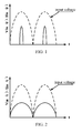
- the broken line in FIG. 1 shows the output terminal voltage waveform of the bridge rectifier of the input terminal grid; the solid line shows the output terminal current waveform of the bridge rectifier of the input terminal grid. As shown in the figure, the outputted current waveform has a serious distortion, meanwhile, the power factor is much low.
- the internal electronic components may be burned when the output voltage exceeds the rated value; for only a single static over-voltage protection in the power factor correction controller, when the load changes, the irreversible damage to the electronic components may be caused when the output voltage instantaneously rises over the rated value. Accordingly, when the output voltage of the power factor correction controller exceeds the rated value (static or dynamic), the protection circuit should provide an effective protection for the electronic components, which is the problems desiderate to be solved.
- the present invention provides an output over-voltage protection circuit for power factor correction to effectively solve the above problems that there is no output over-voltage circuit or only a single static over-voltage circuit in the conventional power factor correction.
- the transient response capability of power factor correction for the output over-voltage circuit is enhanced.
- the present invention provides an effective protection for the power factor corrector and peripheral electronic devices by controlling the logic circuit to shutdown the power tube when an output over-voltage occurs.
- the output over-voltage protection circuit for power factor correction includes an off-chip compensation network, an off-chip resistive divider network, a static over-voltage detection circuit, a dynamic over-voltage detection circuit, and a comparator circuit.
- the off-chip compensation network is coupled between the off-chip resistive divider network and the dynamic over-voltage detection circuit.
- the off-chip compensation network is configured to convert a dynamic over-voltage signal to a dynamic current signal and transmit the dynamic current signal to the dynamic over-voltage detection circuit.
- the dynamic over-voltage detection circuit is configured to detect the dynamic current signal and generate a dynamic over-voltage signal DYOVP.
- the dynamic over-voltage signal DYOVP is inputted into the comparator circuit.
- the comparator circuit is configured to convert the dynamic over-voltage signal DYOVP to a voltage and compare the voltage with a reference voltage and output an over-voltage control signal OVP so as to perform a dynamic over-voltage protection function.
- the off-chip compensation network consists of a resistor R3, a capacitor C1, and a capacitor C2.
- An end of the capacitor C1 is used as an end of the off-chip compensation network and is connected to an end of the capacitor C2; the other end of the capacitor C1 is connected to the resistor R3; the other end of the capacitor C2 and the other end of the resistor R3 are connected together being as the other end of the off-chip compensation network and also an input terminal of the dynamic over-voltage detection circuit, the terminal is also an output terminal COMP of an error amplifier circuit.
- the off-chip resistive divider network consists of a resistor R1 and a resistor R2. An end of the resistor R1 is connected to an output voltage V OUT of a power factor correction controller; the other end of the resistor R1 and an end of the R2 are connected together and are used as an input terminal of the off-chip compensation network and the static over-voltage detection circuit; the other end of the resistor R2 is connected to a ground GND.
- the static over-voltage detection circuit includes a differential input stage circuit, an intermediate amplifier circuit, and a low clamp circuit.
- a non-inverting input end of the differential input stage circuit is connected to an output terminal of the off-chip resistive divider network; an inverting input end is connected to a reference voltage Vref1, the output terminal is connected to an input terminal of the intermediate amplifier circuit.
- the intermediate amplifier circuit consists of a transistor Q4 and a capacitor C3. A base of the transistor Q4 and an end of the capacitor C3 are connected together and then connected to an input terminal of a differential input stage. A collector of the transistor Q4 and the other end of the capacitor C3 are connected together and then connected to an emitter of a low clamping switch Q3 being as an output terminal of the intermediate amplifier circuit.
- the intermediate amplifier is configured to perform a secondary amplification for an output signal of the differential input stage.
- the low clamp circuit consists of a transistor Q1, a transistor Q2, a transistor Q3, and a current bias I bias .
- An emitter of the transistor Q1 and an emitter of the transistor Q2 are connected to a volt current condenser VCC.
- a base and a collector of the transistor Q1 are connected together to be an end connected to a collector of the transistor Q3.
- a collector of the transistor Q2 is configured to output a static over-voltage signal STOVP to an input terminal of the comparator circuit.
- a base of the transistor Q3 is connected to a reference voltage Vref2; the Vref2 is a low clamping voltage of an output terminal COMP of an error amplifier.
- An emitter of the transistor Q3 is connected to an output terminal of an intermediate amplifier circuit.
- the current bias I bias provides a current needed to mirror output to STOVP when the low clamping circuit occurs.
- the dynamic over-voltage detection circuit includes an AB push-pull output stage circuit and a dynamic current mirror circuit.
- An input terminal of the AB push-pull output stage circuit is connected to an output terminal of an intermediate amplifier circuit; the other end of the AB push-pull output stage circuit is connected to a bias circuit; the bias circuit is configured to provide a constant bias for the AB push-pull output stage circuit.
- An output terminal of the AB push-pull output stage circuit is connected to an input terminal of the dynamic current mirror circuit; the other output terminal is a COMP.
- the output terminal is connected to an output terminal of the off-chip compensation network, thus the COMP terminal is also an input terminal of the dynamic over-voltage detection circuit.
- the AB push-pull output stage circuit consists of a transistor Q11, a transistor Q12, a transistor Q5, a transistor Q7, a transistor Q8, a transistor Q9, a resistor R4, a resistor R6, and a resistor R8.
- a base and a collector of the transistor Q11 are connected together and then connected to a base of the transistor Q12 and an end of the resistor R8; the other end of resistor R8 is connected to an emitter of the transistor Q12 and also connected to an output terminal of the intermediate amplifier circuit.
- An emitter of the transistor Q12 is connected to a base of the transistor Q8; an emitter of the transistor Q11 and a collector of the transistor Q12 are connected together to connect to a bias circuit, the emitter of the transistor Q11 is also connected to a base of the transistor Q7.
- An end of the resistor R4 is connected to the volt current condenser VCC; the other end of the resistor R4 is connected to an emitter of the transistor Q5.
- a base and a collector of the transistor Q5 are connected together to connect to a collector of the transistor Q5 and a base of the transistor Q6.
- An emitter of the transistor Q7 and an emitter of the transistor Q8 are connected together being as an output terminal VCOMP of the AB push-pull output stage circuit, and the end is also connected to the off-chip compensation network.
- the off-chip compensation network is configured to provide a dynamic current I ST to a COMP when the dynamic over-voltage occurs.
- a collector of the transistor Q8, a base and an emitter of the transistor Q9 are connected together; a base of the transistor Q9 and a base of the transistor Q10 are connected together; the emitter of the transistor Q9 is connected to an end of the resistor R6, the other end of the resistor R6 is connected to a ground GND.
- the dynamic current mirror circuit consists of a resistor R5, a resistor R7, a transistor Q6, and a transistor Q10.
- An end of the resistor R5 is connected to a volt current condenser VCC, the other end of the resistor R5 is connected to an emitter of the transistor Q6.
- a base of the transistor Q6 and a base of the transistor Q5 are connected together to be an input terminal of a dynamic mirror circuit.
- An emitter of the transistor Q6 and an emitter of the transistor Q10 are connected together being as output terminal of the dynamic over-voltage signal and also being as an input terminal of the comparator circuit.
- a base of the transistor Q10 and a base of the transistor Q9 are connected together.
- An emitter of the transistor Q10 is connected to an end of the resistor R7, the other end of the resistor R7 is connected to a ground GNP.
- the present invention has the following advantages:
- the present invention provides two over-voltage protection modes for the output voltage, which are static over-voltage protection and dynamic over-voltage protection, thus the problems that there is no effective output over-voltage protection or only a single static over-voltage protection in the conventional power factor correction controller is effectively solved.
- the present invention implements a sampling of the dynamic over-voltage signal using the off-chip compensation network without additional electronic components. No cost increases while the system stability and reliability are improved.
- the output over-voltage protection circuit of the present invention includes: an off-chip resistive divider network, an off-chip compensation network, a static over-voltage detection circuit, a dynamic over-voltage detection circuit, and a comparator circuit.
- the off-chip compensation network is coupled between the off-chip resistive divider network and the dynamic over-voltage detection circuit.
- the off-chip compensation network is configured to convert a dynamic over-voltage signal to a dynamic current signal and transmit the dynamic current signal to the dynamic over-voltage detection circuit.
- the dynamic over-voltage detection circuit is configured to detect the dynamic current signal and generate a dynamic over-voltage signal DYOVP; the dynamic over-voltage signal DYOVP is inputted into the comparator circuit, the comparator circuit is configured to convert the dynamic over-voltage signal DYOVP to a voltage and compare the voltage with a reference voltage and then output an over-voltage control signal OVP so as to perform a dynamic over-voltage protection function.
- the over-voltage protection circuit implements dynamic over-voltage protection or static over-voltage protection according to the short-term behavior or long-term behavior of the output voltage over-voltage, respectively.
- the specific manner is: when the output voltage of the power factor correction controller suddenly increases to exceed the rated voltage due to load changes and other reasons, since the bandwidth of the error amplifier circuit is very narrow, its feedback input voltage V FB maintains in a stable reference voltage provided by a reference source circuit, the transient large current will pass through the off-chip compensation network and enter the output terminal COMP of the error amplification circuit.
- the COMP terminal is connected to the input terminal of the dynamic detection circuit, which is configured to detect the transient large current and output the dynamic over-voltage signal DYOVP, the comparator circuit is configured to convert the current signal to a voltage and compare the voltage with the reference voltage, and then the over-voltage control signal OVP is outputted.
- the reference current generated by the reference source circuit is mirrored out to be static over-voltage detection signal STOVP when the low clamping circuit of the output terminal of the error amplifier occurs, this signal is configured to be an input terminal of the comparator circuit, and is compared with the internal reference current of the comparator circuit and the over-voltage signal OVP is outputted.
- the over-voltage signal OVP is outputted, and it then enters the logic circuit to shutdown the power tube.
- the bandwidth of the error amplifier in the power factor correction controller is narrow, it is difficult to make the correct response when the output voltage instantaneously exceeds the rated voltage, this problem is effectively solved by the present invention using the output over-voltage protection circuit, and the transient response for the output over-voltage of the power factor correction controller is improved.
- the static over-voltage detection circuit can provide an effective output; the effective output passes through the comparison circuit and the logic circuit, then shutdowns the power tube. Accordingly, for both dynamic over-voltage and static over-voltage, the present invention can make the right response and provide an effective protection for the power factor correction controller and its peripheral electronic components.
- each unit circuit of the present invention is as follows:
- the off-chip compensation network is coupled between the output terminal V OUT of the power factor correction and the input terminal FB of the differential input stage of the error amplifier.
- the voltage V FB of the input terminal FB of the differential input stage maintains at a high level. Since the other input terminal of the differential input stage is the reference voltage Vref1 provided by the reference source circuit, the difference signal of the V FB and the Vref1 is amplified, the output voltage of the differential input stage is at the high level.
- the output terminal of the differential input stage is connected to the input terminal of the intermediate amplifier circuit, i.e. a base of the transistor Q4.
- the output voltage of the differential input stage is higher than the threshold voltage of the transistor Q4, while a collector of the transistor Q4 is pulled to a low level. Since the voltage of the base of the transistor Q3 is the reference voltage Vref2 provided by the reference source circuit.
- the transistor Q4 When the base of the transistor Q4 is pulled down, the voltage (V BE ) of the base (B) - the emitter (E) of the transistor Q3 exceeds the turn-on voltage drop of the transistor, the transistor Q3 is turned on; in the condition that transistor Q3 and transistor Q4 are turned on at the same time, the current path VCC-Q1-Q3-Q4-Ibias-GND is generated between the voltage VCC to GND.
- the reference current I bias provided by the reference source circuit will flow through the transistor Q1.
- the current mirror circuit consists of the transistor Q1 and transistor Q2, thus the current I bias will be mirrored as static an over-voltage detection output signal STOVP; the static over-voltage detection output signal STOV enters into the comparison circuit, the comparator circuit compares the current with the internal reference current of the circuit and then produces the output over-voltage signal OVP, the signal OVP enters into the logic circuit and shutdowns the power tube after passing through the logic circuit.
- the over-voltage signal OVP is outputted, and enters into the logic circuit to shutdown the power tube.
- the problems that there is no output over-voltage circuit or only a single static over-voltage circuit in the conventional power factor correction controller are effectively solved.
Landscapes
- Engineering & Computer Science (AREA)
- Power Engineering (AREA)
- Continuous-Control Power Sources That Use Transistors (AREA)
- Amplifiers (AREA)
- Protection Of Static Devices (AREA)
- Emergency Protection Circuit Devices (AREA)
Abstract
Description
- The present invention relates to a field of electronic circuit technology, which also relates to analog integrated circuits, and more particularly relates to an output over-voltage protection circuit for power factor correction, which is applied to the output over-voltage protection in the power factor correction controller.
- Switching mode power supply with alternating current input is a typical electronic system, which has a wide range of applications, and a number of the switching mode power supply applied in the application is great. Most of the input rectifier filter in the internal thereof consists of uncontrolled rectifier circuits and capacitor filter circuits composed of diodes. Due to this, the problems of harmonic pollution and lower power factor of the switching mode power supply are generated. In order to improve the efficiency of the switching mode power supply and reduce the grid pollution, the power factor correction technology is increasingly becoming a hot topic in the power supply design field.
- In the switching mode power supply, any circuit that makes the input grid current be non-sinusoidal, or makes the sine wave and the sinusoidal input voltage be in different phases, or makes the input current have harmonic will reduce the power factor PF, thereby resulting in power loss. The use of the power factor correction controller (PFC) is one of the most effective methods to improve the power factor of electronic products and reduce harmonic interference. The broken line in
FIG. 1 shows the output terminal voltage waveform of the bridge rectifier of the input terminal grid; the solid line shows the output terminal current waveform of the bridge rectifier of the input terminal grid. As shown in the figure, the outputted current waveform has a serious distortion, meanwhile, the power factor is much low. The waveforms shown inFIG. 2 are the input voltage waveform and the current waveform after using the power factor correction controller, the broken line therein shows the output terminal voltage waveform of the bridge rectifier of the input terminal grid; the solid line shows the output terminal current waveform of the bridge rectifier of the input terminal grid. The output current waveform strictly follows the input voltage waveform; the power factor is close to 1. - However, currently, there is no effective output over-voltage protection function or only a single static over-voltage protection in the power factor correction controller. For the power factor correction controller without output over-voltage protection function, the internal electronic components may be burned when the output voltage exceeds the rated value; for only a single static over-voltage protection in the power factor correction controller, when the load changes, the irreversible damage to the electronic components may be caused when the output voltage instantaneously rises over the rated value. Accordingly, when the output voltage of the power factor correction controller exceeds the rated value (static or dynamic), the protection circuit should provide an effective protection for the electronic components, which is the problems desiderate to be solved.
- In order to overcome the disadvantages of the prior art, the present invention provides an output over-voltage protection circuit for power factor correction to effectively solve the above problems that there is no output over-voltage circuit or only a single static over-voltage circuit in the conventional power factor correction. The transient response capability of power factor correction for the output over-voltage circuit is enhanced. The present invention provides an effective protection for the power factor corrector and peripheral electronic devices by controlling the logic circuit to shutdown the power tube when an output over-voltage occurs.
- The object of the present invention is obtained by the following technical solution:
- The output over-voltage protection circuit for power factor correction includes an off-chip compensation network, an off-chip resistive divider network, a static over-voltage detection circuit, a dynamic over-voltage detection circuit, and a comparator circuit. The off-chip compensation network is coupled between the off-chip resistive divider network and the dynamic over-voltage detection circuit. The off-chip compensation network is configured to convert a dynamic over-voltage signal to a dynamic current signal and transmit the dynamic current signal to the dynamic over-voltage detection circuit. The dynamic over-voltage detection circuit is configured to detect the dynamic current signal and generate a dynamic over-voltage signal DYOVP. The dynamic over-voltage signal DYOVP is inputted into the comparator circuit. The comparator circuit is configured to convert the dynamic over-voltage signal DYOVP to a voltage and compare the voltage with a reference voltage and output an over-voltage control signal OVP so as to perform a dynamic over-voltage protection function.
- The off-chip compensation network consists of a resistor R3, a capacitor C1, and a capacitor C2. An end of the capacitor C1 is used as an end of the off-chip compensation network and is connected to an end of the capacitor C2; the other end of the capacitor C1 is connected to the resistor R3; the other end of the capacitor C2 and the other end of the resistor R3 are connected together being as the other end of the off-chip compensation network and also an input terminal of the dynamic over-voltage detection circuit, the terminal is also an output terminal COMP of an error amplifier circuit.
- The off-chip resistive divider network consists of a resistor R1 and a resistor R2. An end of the resistor R1 is connected to an output voltage VOUT of a power factor correction controller; the other end of the resistor R1 and an end of the R2 are connected together and are used as an input terminal of the off-chip compensation network and the static over-voltage detection circuit; the other end of the resistor R2 is connected to a ground GND.
- The static over-voltage detection circuit includes a differential input stage circuit, an intermediate amplifier circuit, and a low clamp circuit. A non-inverting input end of the differential input stage circuit is connected to an output terminal of the off-chip resistive divider network; an inverting input end is connected to a reference voltage Vref1, the output terminal is connected to an input terminal of the intermediate amplifier circuit.
- The intermediate amplifier circuit consists of a transistor Q4 and a capacitor C3. A base of the transistor Q4 and an end of the capacitor C3 are connected together and then connected to an input terminal of a differential input stage. A collector of the transistor Q4 and the other end of the capacitor C3 are connected together and then connected to an emitter of a low clamping switch Q3 being as an output terminal of the intermediate amplifier circuit. The intermediate amplifier is configured to perform a secondary amplification for an output signal of the differential input stage.
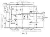
- The low clamp circuit consists of a transistor Q1, a transistor Q2, a transistor Q3, and a current bias Ibias. An emitter of the transistor Q1 and an emitter of the transistor Q2 are connected to a volt current condenser VCC. A base and a collector of the transistor Q1 are connected together to be an end connected to a collector of the transistor Q3. A collector of the transistor Q2 is configured to output a static over-voltage signal STOVP to an input terminal of the comparator circuit. A base of the transistor Q3 is connected to a reference voltage Vref2; the Vref2 is a low clamping voltage of an output terminal COMP of an error amplifier. An emitter of the transistor Q3 is connected to an output terminal of an intermediate amplifier circuit. The current bias Ibias provides a current needed to mirror output to STOVP when the low clamping circuit occurs.
- The dynamic over-voltage detection circuit includes an AB push-pull output stage circuit and a dynamic current mirror circuit. An input terminal of the AB push-pull output stage circuit is connected to an output terminal of an intermediate amplifier circuit; the other end of the AB push-pull output stage circuit is connected to a bias circuit; the bias circuit is configured to provide a constant bias for the AB push-pull output stage circuit. An output terminal of the AB push-pull output stage circuit is connected to an input terminal of the dynamic current mirror circuit; the other output terminal is a COMP. The output terminal is connected to an output terminal of the off-chip compensation network, thus the COMP terminal is also an input terminal of the dynamic over-voltage detection circuit.
- The AB push-pull output stage circuit consists of a transistor Q11, a transistor Q12, a transistor Q5, a transistor Q7, a transistor Q8, a transistor Q9, a resistor R4, a resistor R6, and a resistor R8. A base and a collector of the transistor Q11 are connected together and then connected to a base of the transistor Q12 and an end of the resistor R8; the other end of resistor R8 is connected to an emitter of the transistor Q12 and also connected to an output terminal of the intermediate amplifier circuit. An emitter of the transistor Q12 is connected to a base of the transistor Q8; an emitter of the transistor Q11 and a collector of the transistor Q12 are connected together to connect to a bias circuit, the emitter of the transistor Q11 is also connected to a base of the transistor Q7. An end of the resistor R4 is connected to the volt current condenser VCC; the other end of the resistor R4 is connected to an emitter of the transistor Q5. A base and a collector of the transistor Q5 are connected together to connect to a collector of the transistor Q5 and a base of the transistor Q6. An emitter of the transistor Q7 and an emitter of the transistor Q8 are connected together being as an output terminal VCOMP of the AB push-pull output stage circuit, and the end is also connected to the off-chip compensation network. The off-chip compensation network is configured to provide a dynamic current IST to a COMP when the dynamic over-voltage occurs. A collector of the transistor Q8, a base and an emitter of the transistor Q9 are connected together; a base of the transistor Q9 and a base of the transistor Q10 are connected together; the emitter of the transistor Q9 is connected to an end of the resistor R6, the other end of the resistor R6 is connected to a ground GND.
- The dynamic current mirror circuit consists of a resistor R5, a resistor R7, a transistor Q6, and a transistor Q10. An end of the resistor R5 is connected to a volt current condenser VCC, the other end of the resistor R5 is connected to an emitter of the transistor Q6. A base of the transistor Q6 and a base of the transistor Q5 are connected together to be an input terminal of a dynamic mirror circuit. An emitter of the transistor Q6 and an emitter of the transistor Q10 are connected together being as output terminal of the dynamic over-voltage signal and also being as an input terminal of the comparator circuit. A base of the transistor Q10 and a base of the transistor Q9 are connected together. An emitter of the transistor Q10 is connected to an end of the resistor R7, the other end of the resistor R7 is connected to a ground GNP.
- Compared with the prior art, the present invention has the following advantages:
- 1. The present invention provides two over-voltage protection modes for the output voltage, which are static over-voltage protection and dynamic over-voltage protection, thus the problems that there is no effective output over-voltage protection or only a single static over-voltage protection in the conventional power factor correction controller is effectively solved.
- 2. The present invention implements a sampling of the dynamic over-voltage signal using the off-chip compensation network without additional electronic components. No cost increases while the system stability and reliability are improved.
- 3. Both over-voltage detection circuits provided by the present invention are integrated into the error amplifier circuit; this design simplifies the circuit and greatly reduces the actual layout area. Cost is saved and a much smaller chip is obtained while the system stability and reliability are improved.
-
-
FIG. 1 is a graph showing the input voltage waveform and the input current waveform without using a power factor correction; -
FIG. 2 is a chart showing the input voltage waveform and the input current waveform using a power factor correction; -
FIG. 3 illustrates a block diagram of a circuit according to the present invention; and -
FIG. 4 illustrates a schematic circuit diagram of the present invention. - Reference will now be made to the drawings to describe, in detail, embodiments of the present invention.
- For convenience of description, the present invention provides a block diagram of the output over-voltage protection circuit used in power factor correction controller, which is shown in
FIG. 3 . The output over-voltage protection circuit of the present invention includes: an off-chip resistive divider network, an off-chip compensation network, a static over-voltage detection circuit, a dynamic over-voltage detection circuit, and a comparator circuit. The off-chip compensation network is coupled between the off-chip resistive divider network and the dynamic over-voltage detection circuit. The off-chip compensation network is configured to convert a dynamic over-voltage signal to a dynamic current signal and transmit the dynamic current signal to the dynamic over-voltage detection circuit. The dynamic over-voltage detection circuit is configured to detect the dynamic current signal and generate a dynamic over-voltage signal DYOVP; the dynamic over-voltage signal DYOVP is inputted into the comparator circuit, the comparator circuit is configured to convert the dynamic over-voltage signal DYOVP to a voltage and compare the voltage with a reference voltage and then output an over-voltage control signal OVP so as to perform a dynamic over-voltage protection function. In the illustrated embodiment, the over-voltage protection circuit implements dynamic over-voltage protection or static over-voltage protection according to the short-term behavior or long-term behavior of the output voltage over-voltage, respectively. Referring toFIG.3 , the specific manner is: when the output voltage of the power factor correction controller suddenly increases to exceed the rated voltage due to load changes and other reasons, since the bandwidth of the error amplifier circuit is very narrow, its feedback input voltage VFB maintains in a stable reference voltage provided by a reference source circuit, the transient large current will pass through the off-chip compensation network and enter the output terminal COMP of the error amplification circuit. The COMP terminal is connected to the input terminal of the dynamic detection circuit, which is configured to detect the transient large current and output the dynamic over-voltage signal DYOVP, the comparator circuit is configured to convert the current signal to a voltage and compare the voltage with the reference voltage, and then the over-voltage control signal OVP is outputted. If the output voltage of the power factor correction controller slowly increases to exceed the rated voltage or suddenly increases to exceed the rated voltage due to load changes and other reasons, and all the output voltages do not drop to the normal value in a short period of time, the reference current generated by the reference source circuit is mirrored out to be static over-voltage detection signal STOVP when the low clamping circuit of the output terminal of the error amplifier occurs, this signal is configured to be an input terminal of the comparator circuit, and is compared with the internal reference current of the comparator circuit and the over-voltage signal OVP is outputted. In the present invention, for both the dynamic over-voltage and the static over-voltage, the over-voltage signal OVP is outputted, and it then enters the logic circuit to shutdown the power tube. Since the bandwidth of the error amplifier in the power factor correction controller is narrow, it is difficult to make the correct response when the output voltage instantaneously exceeds the rated voltage, this problem is effectively solved by the present invention using the output over-voltage protection circuit, and the transient response for the output over-voltage of the power factor correction controller is improved. Meanwhile, if the output voltage is always in a steady-state that exceeds the rated voltage, the static over-voltage detection circuit can provide an effective output; the effective output passes through the comparison circuit and the logic circuit, then shutdowns the power tube. Accordingly, for both dynamic over-voltage and static over-voltage, the present invention can make the right response and provide an effective protection for the power factor correction controller and its peripheral electronic components. - Referring to
FIG. 3 andFIG. 4 , the structure and working principle of each unit circuit of the present invention are as follows: - The off-chip compensation network is coupled between the output terminal VOUT of the power factor correction and the input terminal FB of the differential input stage of the error amplifier. When the output voltage of the power factor correction controller slowly increases to exceed the rated voltage or suddenly increases to exceed the rated voltage due to load changes and other reasons, and all the output voltage VOUT do not drop to the normal value in a short period of time, the voltage VFB of the input terminal FB of the differential input stage maintains at a high level. Since the other input terminal of the differential input stage is the reference voltage Vref1 provided by the reference source circuit, the difference signal of the VFB and the Vref1 is amplified, the output voltage of the differential input stage is at the high level. The output terminal of the differential input stage is connected to the input terminal of the intermediate amplifier circuit, i.e. a base of the transistor Q4. The output voltage of the differential input stage is higher than the threshold voltage of the transistor Q4, while a collector of the transistor Q4 is pulled to a low level. Since the voltage of the base of the transistor Q3 is the reference voltage Vref2 provided by the reference source circuit. When the base of the transistor Q4 is pulled down, the voltage (VBE) of the base (B) - the emitter (E) of the transistor Q3 exceeds the turn-on voltage drop of the transistor, the transistor Q3 is turned on; in the condition that transistor Q3 and transistor Q4 are turned on at the same time, the current path VCC-Q1-Q3-Q4-Ibias-GND is generated between the voltage VCC to GND. The reference current Ibias provided by the reference source circuit will flow through the transistor Q1. The current mirror circuit consists of the transistor Q1 and transistor Q2, thus the current Ibias will be mirrored as static an over-voltage detection output signal STOVP; the static over-voltage detection output signal STOV enters into the comparison circuit, the comparator circuit compares the current with the internal reference current of the circuit and then produces the output over-voltage signal OVP, the signal OVP enters into the logic circuit and shutdowns the power tube after passing through the logic circuit.
- Since the bandwidth of the error amplifier circuit in the power factor correction controller is very narrow, when the output voltage VOUT instantaneously exceeds the rated voltage value, the feedback terminal voltage VFB of the error amplifier is still equaled to the reference voltage Vref1, when the VOUT instantaneously exceeds the rated voltage, a detection cannot be performed by the static over-voltage detection circuit, i.e. a stable and reliable output over-voltage protection cannot be provided by the static over-voltage detection circuit.
- In a steady state, the adjustment of the off-chip resistive divider network R1 and R2 makes the output voltage VOUT of the power factor correction controller be the rated voltage. If the ripple component is ignored, the current passing through the R1 is IR1, which equals to the current IR2 passing through the R2, taking into account that the inverting input terminal of the input stage of the error amplification circuit is the reference voltage Vref1; therefore, the feedback terminal voltage VFB of the error amplifier circuit is equaled to the reference voltage Vref1, so:

- If there is a great change of ΔV0>0 in the power factor correction controller due to the load changes, the feedback terminal voltage VFB will maintain at Vref1 by the partial feedback of the error amplifier. Accordingly, the current passing through R2 will continue to maintain at Vref1/R2, while the current passing through R1 would become:

- The differential current Ist = ΔIR1=I'R1-IR2=I'R1-IR1=ΔVO/R1 passes through the off-chip compensation network and enters into the output terminal VCMOP of the error amplifier circuit; the current Ist will pass through the AB push-pull output stage circuit and the dynamic of the dynamic current mirror circuit, and then the current is outputted as the dynamic over-voltage signal DYOVP; the dynamic over-voltage signal DYOVP enters into the comparison circuit, the comparison circuit converts the signal to a static voltage and compares it with the reference voltage provided by the reference source circuit, and the output over-voltage signal OVP is outputted, the signal OVP enters the logic circuit and shutdowns the power tube after passing through the logic circuit.
- In the present invention, for both the occurrence of dynamic over-voltage and the static over-voltage, the over-voltage signal OVP is outputted, and enters into the logic circuit to shutdown the power tube. In the present invention, the problems that there is no output over-voltage circuit or only a single static over-voltage circuit in the conventional power factor correction controller are effectively solved.
- Although the present invention has been described with reference to the embodiments thereof and the best modes for carrying out the present invention, it is apparent to those skilled in the art that a variety of modifications and changes may be made without departing from the scope of the present invention, which is intended to be defined by the appended claims.
Claims (9)
- An output over-voltage protection circuit for power factor correction, comprising:an off-chip compensation network, an off-chip resistive divider network, a static over-voltage detection circuit, a dynamic over-voltage detection circuit, and a comparator circuit; wherein the off-chip compensation network is coupled between the off-chip resistive divider network and the dynamic over-voltage detection circuit, the off-chip compensation network is configured to convert a dynamic over-voltage signal to a dynamic current signal and transmit the dynamic current signal to the dynamic over-voltage detection circuit, the dynamic over-voltage detection circuit is configured to detect the dynamic current signal and generate a dynamic over-voltage signal DYOVP; the dynamic over-voltage signal DYOVP is inputted into the comparator circuit; the comparator circuit is configured to convert the dynamic over-voltage signal DYOVP to a voltage and compare the voltage with a reference voltage and output an over-voltage control signal OVP so as to perform a dynamic over-voltage protection function.
- The output over-voltage protection circuit according to claim 1, wherein the off-chip compensation network consists of a resistor R3, a capacitor C1, and a capacitor C2; an end of the capacitor C1 is used as an end of the off-chip compensation network and is connected to an end of the capacitor C2; the other end of the capacitor C1 is connected to the resistor R3; the other end of the capacitor C2 and the other end of the resistor R3 are connected together being as the other end of the off-chip compensation network and also an input terminal of the dynamic over-voltage detection circuit, the terminal is also an output terminal COMP of an error amplifier circuit.
- The output over-voltage protection circuit according to claim 1, wherein the off-chip resistive divider network consists of a resistor R1 and a resistor R2, an end of the resistor R1 is connected to an output voltage VOUT of a power factor correction controller, the other end of the resistor R1 and an end of the R2 are connected together and are used as an input terminal of the off-chip compensation network and the static over-voltage detection circuit; the other end of the resistor R2 is connected to a ground GND.
- The output over-voltage protection circuit according to claim 1, wherein the static over-voltage detection circuit comprises a differential input stage circuit, an intermediate amplifier circuit, and a low clamp circuit; a non-inverting input end of the differential input stage circuit is connected to an output terminal of the off-chip resistive divider network; an inverting input end is connected to a reference voltage Vref1, the output terminal is connected to an input terminal of the intermediate amplifier circuit.
- The output over-voltage protection circuit according to claim 1, wherein the intermediate amplifier circuit consists of a transistor Q4 and a capacitor C3; a base of the transistor Q4 and an end of the capacitor C3 are connected together and then connected to an input terminal of a differential input stage; a collector of the transistor Q4 and the other end of the capacitor C3 are connected together and then connected to an emitter of a low clamping switch Q3 being as an output terminal of the intermediate amplifier circuit; the intermediate amplifier is configured to perform a secondary amplification for an output signal of the differential input stage.
- The output over-voltage protection circuit according to claim 1, wherein the low clamp circuit consists of a transistor Q1, a transistor Q2, a transistor Q3, and a current bias Ibias; an emitter of the transistor Q1 and an emitter of the transistor Q2 are connected to a volt current condenser VCC; a base and a collector of the transistor Q1 are connected together to be an end connected to a collector of the transistor Q3; a collector of the transistor Q2 is configured to output a static over-voltage signal STOVP to an input terminal of the comparator circuit; a base of the transistor Q3 is connected to a reference voltage Vref2; the Vref2 is a low clamping voltage of an output terminal COMP of an error amplifier; an emitter of the transistor Q3 is connected to an output terminal of an intermediate amplifier circuit; the current bias Ibias provides a current needed to mirror output to STOVP when the low clamping circuit occurs.
- The output over-voltage protection circuit according to claim 1, wherein the dynamic over-voltage detection circuit comprises an AB push-pull output stage circuit and a dynamic current mirror circuit; an input terminal of the AB push-pull output stage circuit is connected to an output terminal of an intermediate amplifier circuit; the other end of the AB push-pull output stage circuit is connected to a bias circuit; the bias circuit is configured to provide a constant bias for the AB push-pull output stage circuit; an output terminal of the AB push-pull output stage circuit is connected to an input terminal of the dynamic current mirror circuit, the other output terminal is a COMP, the output terminal is connected to an output terminal of the off-chip compensation network, thus the COMP terminal is also an input terminal of the dynamic over-voltage detection circuit.
- The output over-voltage protection circuit according to claim 1, wherein the AB push-pull output stage circuit consists of a transistor Q11, a transistor Q12, a transistor Q5, a transistor Q7, a transistor Q8, a transistor Q9, a resistor R4, a resistor R6, and a resistor R8; a base and a collector of the transistor Q11 are connected together and then connected to a base of the transistor Q12 and an end of the resistor R8; the other end of resistor R8 is connected to an emitter of the transistor Q12 and also connected to an output terminal of the intermediate amplifier circuit, and an emitter of the transistor Q12 is connected to a base of the transistor Q8; an emitter of the transistor Q11 and a collector of the transistor Q12 are connected together to connect to a bias circuit, the emitter of the transistor Q11 is also connected to a base of the transistor Q7; an end of the resistor R4 is connected to the volt current condenser VCC; the other end of the resistor R4 is connected to an emitter of the transistor Q5; a base and a collector of the transistor Q5 are connected together to connect to a collector of the transistor Q5 and a base of the transistor Q6; an emitter of the transistor Q7 and an emitter of the transistor Q8 are connected together being as an output terminal VCOMP of the AB push-pull output stage circuit, and the end is also connected to the off-chip compensation network, the off-chip compensation network is configured to provide a dynamic current IST to a COMP when the dynamic over-voltage occurs; a collector of the transistor Q8, a base and an emitter of the transistor Q9 are connected together; a base of the transistor Q9 and a base of the transistor Q10 are connected together; the emitter of the transistor Q9 is connected to an end of the resistor R6, the other end of the resistor R6 is connected to a ground GND.
- The output over-voltage protection circuit according to claim 1, wherein the dynamic current mirror circuit consists of a resistor R5, a resistor R7, a transistor Q6, and a transistor Q10; an end of the resistor R5 is connected to a volt current condenser VCC, the other end of the resistor R5 is connected to an emitter of the transistor Q6; a base of the transistor Q6 and a base of the transistor Q5 are connected together to be an input terminal of a dynamic mirror circuit; an emitter of the transistor Q6 and an emitter of the transistor Q10 are connected together being as output terminal of the dynamic over-voltage signal and also being as an input terminal of the comparator circuit; a base of the transistor Q10 and a base of the transistor Q9 are connected together; an emitter of the transistor Q10 is connected to an end of the resistor R7, the other end of the resistor R7 is connected to a ground GNP.
Applications Claiming Priority (2)
| Application Number | Priority Date | Filing Date | Title |
|---|---|---|---|
| CN2011103587894A CN102497093A (en) | 2011-11-11 | 2011-11-11 | Output over-voltage protection circuit for power factor corrector |
| PCT/CN2012/084359 WO2013067957A1 (en) | 2011-11-11 | 2012-11-09 | An output over-voltage protection circuit for power factor correction |
Publications (3)
| Publication Number | Publication Date |
|---|---|
| EP2779344A1 true EP2779344A1 (en) | 2014-09-17 |
| EP2779344A4 EP2779344A4 (en) | 2015-09-02 |
| EP2779344B1 EP2779344B1 (en) | 2021-09-22 |
Family
ID=46188891
Family Applications (1)
| Application Number | Title | Priority Date | Filing Date |
|---|---|---|---|
| EP12848242.9A Active EP2779344B1 (en) | 2011-11-11 | 2012-11-09 | An output over-voltage protection circuit for power factor correction |
Country Status (4)
| Country | Link |
|---|---|
| US (1) | US9379538B2 (en) |
| EP (1) | EP2779344B1 (en) |
| CN (1) | CN102497093A (en) |
| WO (1) | WO2013067957A1 (en) |
Cited By (2)
| Publication number | Priority date | Publication date | Assignee | Title |
|---|---|---|---|---|
| TWI577116B (en) * | 2016-09-07 | 2017-04-01 | 亞源科技股份有限公司 | Over-voltage protection circuit |
| TWI577117B (en) * | 2016-09-07 | 2017-04-01 | 亞源科技股份有限公司 | Over-voltage protection circuit |
Families Citing this family (14)
| Publication number | Priority date | Publication date | Assignee | Title |
|---|---|---|---|---|
| CN102497093A (en) | 2011-11-11 | 2012-06-13 | 无锡华润上华科技有限公司 | Output over-voltage protection circuit for power factor corrector |
| CN104466886B (en) * | 2013-09-18 | 2018-08-10 | 鸿富锦精密工业(深圳)有限公司 | Load protection circuit and load protective method |
| US9342089B2 (en) * | 2014-04-25 | 2016-05-17 | Texas Instruments Deutschland Gmbh | Verification of bandgap reference startup |
| US11211724B2 (en) * | 2015-10-30 | 2021-12-28 | Core Technologies Llc | Small form factor power conversion system |
| US9608616B1 (en) * | 2016-05-27 | 2017-03-28 | Taiwan Semiconductor Manufacturing Company, Ltd. | Power clamp circuits and methods |
| CN105896474B (en) * | 2016-05-30 | 2018-08-28 | 深圳市稳先微电子有限公司 | A kind of output voltage overvoltage crowbar and system for Switching Power Supply |
| CN108039695B (en) * | 2017-11-17 | 2019-07-16 | 深圳市科比特航空科技有限公司 | Overvoltage crowbar |
| CN107834570A (en) * | 2017-11-30 | 2018-03-23 | 浦林成山(山东)轮胎有限公司 | A kind of photovoltaic power generation grid-connecting point power factor regulation device |
| CN112290893B (en) * | 2020-11-07 | 2024-05-28 | 山西大学 | Low Noise Broadband High Voltage Amplifier |
| US12377751B2 (en) | 2020-12-08 | 2025-08-05 | Atom Power, Inc. | Electric vehicle supply equipment unit configured in an EV charging system |
| WO2022125492A1 (en) * | 2020-12-08 | 2022-06-16 | Atom Power, Inc. | Electric vehicle charging system and method |
| CN112994623B (en) * | 2021-05-10 | 2021-08-20 | 杭州中科微电子有限公司 | Power detection circuit applied to power amplifier |
| CN116137524B (en) * | 2023-04-04 | 2023-07-14 | 荣湃半导体(上海)有限公司 | Comparator with high voltage input resistance |
| CN118264078B (en) * | 2024-03-26 | 2025-11-11 | 厦门科华数能科技有限公司 | Conversion circuit layout method and conversion circuit |
Family Cites Families (13)
| Publication number | Priority date | Publication date | Assignee | Title |
|---|---|---|---|---|
| GB1537484A (en) * | 1976-01-27 | 1978-12-29 | Rca Corp | Transistor amplifier with over-current prevention circuitry |
| US4225897A (en) * | 1979-01-29 | 1980-09-30 | Rca Corporation | Overcurrent protection circuit for power transistor |
| US5691889A (en) * | 1995-12-13 | 1997-11-25 | Unitrode Corporation | Controller having feed-forward and synchronization features |
| JP2003318667A (en) * | 2002-04-24 | 2003-11-07 | Fujitsu Ltd | Operational amplifier |
| EP1387475A1 (en) * | 2002-08-01 | 2004-02-04 | STMicroelectronics S.r.l. | Circuit for the programmable protection of output overvoltages in a power factor corrector |
| US6853563B1 (en) * | 2003-07-28 | 2005-02-08 | System General Corp. | Primary-side controlled flyback power converter |
| CN201018409Y (en) | 2007-02-07 | 2008-02-06 | 深圳创维-Rgb电子有限公司 | Overvoltage Protection Circuit of Power Factor Corrector in Power Circuit |
| JP5277952B2 (en) * | 2008-12-25 | 2013-08-28 | 富士電機株式会社 | Switching power supply circuit |
| CN101557162B (en) * | 2009-03-11 | 2011-06-15 | 西安民展微电子有限公司 | Overvoltage protection circuit used in power factor corrector and power factor corrector |
| JP5573454B2 (en) * | 2009-11-26 | 2014-08-20 | 富士電機株式会社 | Power factor improved switching power supply |
| KR101005557B1 (en) * | 2010-08-31 | 2011-01-10 | (주)지에이티 | Electronic Ballast for Cold Cathode Fluorescent Lamps |
| CN102035170B (en) | 2011-01-18 | 2013-06-12 | 福建捷联电子有限公司 | PFC output overvoltage protection circuit |
| CN102497093A (en) | 2011-11-11 | 2012-06-13 | 无锡华润上华科技有限公司 | Output over-voltage protection circuit for power factor corrector |
-
2011
- 2011-11-11 CN CN2011103587894A patent/CN102497093A/en active Pending
-
2012
- 2012-11-09 EP EP12848242.9A patent/EP2779344B1/en active Active
- 2012-11-09 US US14/357,724 patent/US9379538B2/en active Active
- 2012-11-09 WO PCT/CN2012/084359 patent/WO2013067957A1/en not_active Ceased
Cited By (3)
| Publication number | Priority date | Publication date | Assignee | Title |
|---|---|---|---|---|
| TWI577116B (en) * | 2016-09-07 | 2017-04-01 | 亞源科技股份有限公司 | Over-voltage protection circuit |
| TWI577117B (en) * | 2016-09-07 | 2017-04-01 | 亞源科技股份有限公司 | Over-voltage protection circuit |
| US9954457B2 (en) | 2016-09-07 | 2018-04-24 | Asian Power Devices Inc. | Overvoltage protection circuit |
Also Published As
| Publication number | Publication date |
|---|---|
| CN102497093A (en) | 2012-06-13 |
| US9379538B2 (en) | 2016-06-28 |
| WO2013067957A1 (en) | 2013-05-16 |
| EP2779344B1 (en) | 2021-09-22 |
| US20140268464A1 (en) | 2014-09-18 |
| EP2779344A4 (en) | 2015-09-02 |
Similar Documents
| Publication | Publication Date | Title |
|---|---|---|
| EP2779344B1 (en) | An output over-voltage protection circuit for power factor correction | |
| CN110018707B (en) | Low dropout linear regulator circuit with overcurrent protection | |
| CN103546035B (en) | Flyback structure-based power conversion device and power conversion method thereof | |
| TWI565221B (en) | Inverting apparatus and photovoltaic power system using the same | |
| CN109061272B (en) | Current detection circuit | |
| CN107290581B (en) | Current detection circuit of switch circuit and switch circuit | |
| US20080157727A1 (en) | Power factor correction apparatus | |
| CN103475214A (en) | Switch converter and control circuit and control method thereof | |
| CN205453099U (en) | Sampling circuit and mistake, undervoltage protection control circuit | |
| CN101951135A (en) | Flyback switching power supply and over-current protection method thereof | |
| CN110504832B (en) | Control circuit and method for high-voltage BUCK switch converter | |
| CN104571241A (en) | Voltage stabilizing circuit and method thereof | |
| US10164537B2 (en) | Switching regulator | |
| CN201611361U (en) | Overcurrent detection circuit | |
| US12381476B2 (en) | Voltage converter with over-current protection and over-current protection method thereof | |
| US20170126128A1 (en) | Boost converter and the method thereof | |
| CN116470470A (en) | Over-temperature protection circuit, control circuit and over-temperature protection method of switching power supply | |
| US20160072389A1 (en) | Multiple-phase power circuit | |
| CN206931988U (en) | High reliability under-voltage protecting circuit and power supply | |
| US11362510B2 (en) | Power supply device for eliminating malfunction of overcurrent protection | |
| CN210640810U (en) | High-voltage BUCK switch converter and related integrated circuit | |
| KR20130084199A (en) | Single power stage power factor correction circuit | |
| CN212695707U (en) | MOSFET surge protection circuit | |
| CN111812375B (en) | A current and frequency sampling circuit for automatic power conversion system | |
| CN207833370U (en) | A kind of CMOS LDO and the system for improving its load response characteristic |
Legal Events
| Date | Code | Title | Description |
|---|---|---|---|
| PUAI | Public reference made under article 153(3) epc to a published international application that has entered the european phase |
Free format text: ORIGINAL CODE: 0009012 |
|
| 17P | Request for examination filed |
Effective date: 20140522 |
|
| AK | Designated contracting states |
Kind code of ref document: A1 Designated state(s): AL AT BE BG CH CY CZ DE DK EE ES FI FR GB GR HR HU IE IS IT LI LT LU LV MC MK MT NL NO PL PT RO RS SE SI SK SM TR |
|
| DAX | Request for extension of the european patent (deleted) | ||
| RA4 | Supplementary search report drawn up and despatched (corrected) |
Effective date: 20150804 |
|
| RIC1 | Information provided on ipc code assigned before grant |
Ipc: H02M 1/42 20070101ALI20150729BHEP Ipc: H02H 7/10 20060101AFI20150729BHEP |
|
| STAA | Information on the status of an ep patent application or granted ep patent |
Free format text: STATUS: EXAMINATION IS IN PROGRESS |
|
| 17Q | First examination report despatched |
Effective date: 20180530 |
|
| GRAP | Despatch of communication of intention to grant a patent |
Free format text: ORIGINAL CODE: EPIDOSNIGR1 |
|
| STAA | Information on the status of an ep patent application or granted ep patent |
Free format text: STATUS: GRANT OF PATENT IS INTENDED |
|
| INTG | Intention to grant announced |
Effective date: 20210416 |
|
| GRAS | Grant fee paid |
Free format text: ORIGINAL CODE: EPIDOSNIGR3 |
|
| GRAA | (expected) grant |
Free format text: ORIGINAL CODE: 0009210 |
|
| STAA | Information on the status of an ep patent application or granted ep patent |
Free format text: STATUS: THE PATENT HAS BEEN GRANTED |
|
| AK | Designated contracting states |
Kind code of ref document: B1 Designated state(s): AL AT BE BG CH CY CZ DE DK EE ES FI FR GB GR HR HU IE IS IT LI LT LU LV MC MK MT NL NO PL PT RO RS SE SI SK SM TR |
|
| REG | Reference to a national code |
Ref country code: GB Ref legal event code: FG4D |
|
| REG | Reference to a national code |
Ref country code: DE Ref legal event code: R096 Ref document number: 602012076759 Country of ref document: DE |
|
| REG | Reference to a national code |
Ref country code: IE Ref legal event code: FG4D |
|
| REG | Reference to a national code |
Ref country code: CH Ref legal event code: EP Ref country code: AT Ref legal event code: REF Ref document number: 1433055 Country of ref document: AT Kind code of ref document: T Effective date: 20211015 |
|
| REG | Reference to a national code |
Ref country code: LT Ref legal event code: MG9D |
|
| REG | Reference to a national code |
Ref country code: NL Ref legal event code: MP Effective date: 20210922 |
|
| PG25 | Lapsed in a contracting state [announced via postgrant information from national office to epo] |
Ref country code: HR Free format text: LAPSE BECAUSE OF FAILURE TO SUBMIT A TRANSLATION OF THE DESCRIPTION OR TO PAY THE FEE WITHIN THE PRESCRIBED TIME-LIMIT Effective date: 20210922 Ref country code: SE Free format text: LAPSE BECAUSE OF FAILURE TO SUBMIT A TRANSLATION OF THE DESCRIPTION OR TO PAY THE FEE WITHIN THE PRESCRIBED TIME-LIMIT Effective date: 20210922 Ref country code: BG Free format text: LAPSE BECAUSE OF FAILURE TO SUBMIT A TRANSLATION OF THE DESCRIPTION OR TO PAY THE FEE WITHIN THE PRESCRIBED TIME-LIMIT Effective date: 20211222 Ref country code: LT Free format text: LAPSE BECAUSE OF FAILURE TO SUBMIT A TRANSLATION OF THE DESCRIPTION OR TO PAY THE FEE WITHIN THE PRESCRIBED TIME-LIMIT Effective date: 20210922 Ref country code: RS Free format text: LAPSE BECAUSE OF FAILURE TO SUBMIT A TRANSLATION OF THE DESCRIPTION OR TO PAY THE FEE WITHIN THE PRESCRIBED TIME-LIMIT Effective date: 20210922 Ref country code: NO Free format text: LAPSE BECAUSE OF FAILURE TO SUBMIT A TRANSLATION OF THE DESCRIPTION OR TO PAY THE FEE WITHIN THE PRESCRIBED TIME-LIMIT Effective date: 20211222 Ref country code: FI Free format text: LAPSE BECAUSE OF FAILURE TO SUBMIT A TRANSLATION OF THE DESCRIPTION OR TO PAY THE FEE WITHIN THE PRESCRIBED TIME-LIMIT Effective date: 20210922 |
|
| REG | Reference to a national code |
Ref country code: AT Ref legal event code: MK05 Ref document number: 1433055 Country of ref document: AT Kind code of ref document: T Effective date: 20210922 |
|
| PG25 | Lapsed in a contracting state [announced via postgrant information from national office to epo] |
Ref country code: LV Free format text: LAPSE BECAUSE OF FAILURE TO SUBMIT A TRANSLATION OF THE DESCRIPTION OR TO PAY THE FEE WITHIN THE PRESCRIBED TIME-LIMIT Effective date: 20210922 Ref country code: GR Free format text: LAPSE BECAUSE OF FAILURE TO SUBMIT A TRANSLATION OF THE DESCRIPTION OR TO PAY THE FEE WITHIN THE PRESCRIBED TIME-LIMIT Effective date: 20211223 |
|
| PG25 | Lapsed in a contracting state [announced via postgrant information from national office to epo] |
Ref country code: AT Free format text: LAPSE BECAUSE OF FAILURE TO SUBMIT A TRANSLATION OF THE DESCRIPTION OR TO PAY THE FEE WITHIN THE PRESCRIBED TIME-LIMIT Effective date: 20210922 |
|
| PG25 | Lapsed in a contracting state [announced via postgrant information from national office to epo] |
Ref country code: IS Free format text: LAPSE BECAUSE OF FAILURE TO SUBMIT A TRANSLATION OF THE DESCRIPTION OR TO PAY THE FEE WITHIN THE PRESCRIBED TIME-LIMIT Effective date: 20220122 Ref country code: SK Free format text: LAPSE BECAUSE OF FAILURE TO SUBMIT A TRANSLATION OF THE DESCRIPTION OR TO PAY THE FEE WITHIN THE PRESCRIBED TIME-LIMIT Effective date: 20210922 Ref country code: RO Free format text: LAPSE BECAUSE OF FAILURE TO SUBMIT A TRANSLATION OF THE DESCRIPTION OR TO PAY THE FEE WITHIN THE PRESCRIBED TIME-LIMIT Effective date: 20210922 Ref country code: PT Free format text: LAPSE BECAUSE OF FAILURE TO SUBMIT A TRANSLATION OF THE DESCRIPTION OR TO PAY THE FEE WITHIN THE PRESCRIBED TIME-LIMIT Effective date: 20220124 Ref country code: PL Free format text: LAPSE BECAUSE OF FAILURE TO SUBMIT A TRANSLATION OF THE DESCRIPTION OR TO PAY THE FEE WITHIN THE PRESCRIBED TIME-LIMIT Effective date: 20210922 Ref country code: NL Free format text: LAPSE BECAUSE OF FAILURE TO SUBMIT A TRANSLATION OF THE DESCRIPTION OR TO PAY THE FEE WITHIN THE PRESCRIBED TIME-LIMIT Effective date: 20210922 Ref country code: ES Free format text: LAPSE BECAUSE OF FAILURE TO SUBMIT A TRANSLATION OF THE DESCRIPTION OR TO PAY THE FEE WITHIN THE PRESCRIBED TIME-LIMIT Effective date: 20210922 Ref country code: EE Free format text: LAPSE BECAUSE OF FAILURE TO SUBMIT A TRANSLATION OF THE DESCRIPTION OR TO PAY THE FEE WITHIN THE PRESCRIBED TIME-LIMIT Effective date: 20210922 Ref country code: CZ Free format text: LAPSE BECAUSE OF FAILURE TO SUBMIT A TRANSLATION OF THE DESCRIPTION OR TO PAY THE FEE WITHIN THE PRESCRIBED TIME-LIMIT Effective date: 20210922 Ref country code: AL Free format text: LAPSE BECAUSE OF FAILURE TO SUBMIT A TRANSLATION OF THE DESCRIPTION OR TO PAY THE FEE WITHIN THE PRESCRIBED TIME-LIMIT Effective date: 20210922 |
|
| REG | Reference to a national code |
Ref country code: DE Ref legal event code: R097 Ref document number: 602012076759 Country of ref document: DE |
|
| PG25 | Lapsed in a contracting state [announced via postgrant information from national office to epo] |
Ref country code: MC Free format text: LAPSE BECAUSE OF FAILURE TO SUBMIT A TRANSLATION OF THE DESCRIPTION OR TO PAY THE FEE WITHIN THE PRESCRIBED TIME-LIMIT Effective date: 20210922 |
|
| REG | Reference to a national code |
Ref country code: CH Ref legal event code: PL |
|
| PG25 | Lapsed in a contracting state [announced via postgrant information from national office to epo] |
Ref country code: LU Free format text: LAPSE BECAUSE OF NON-PAYMENT OF DUE FEES Effective date: 20211109 Ref country code: DK Free format text: LAPSE BECAUSE OF FAILURE TO SUBMIT A TRANSLATION OF THE DESCRIPTION OR TO PAY THE FEE WITHIN THE PRESCRIBED TIME-LIMIT Effective date: 20210922 Ref country code: BE Free format text: LAPSE BECAUSE OF NON-PAYMENT OF DUE FEES Effective date: 20211130 |
|
| PLBE | No opposition filed within time limit |
Free format text: ORIGINAL CODE: 0009261 |
|
| STAA | Information on the status of an ep patent application or granted ep patent |
Free format text: STATUS: NO OPPOSITION FILED WITHIN TIME LIMIT |
|
| REG | Reference to a national code |
Ref country code: BE Ref legal event code: MM Effective date: 20211130 |
|
| 26N | No opposition filed |
Effective date: 20220623 |
|
| PG25 | Lapsed in a contracting state [announced via postgrant information from national office to epo] |
Ref country code: LI Free format text: LAPSE BECAUSE OF NON-PAYMENT OF DUE FEES Effective date: 20211130 Ref country code: CH Free format text: LAPSE BECAUSE OF NON-PAYMENT OF DUE FEES Effective date: 20211130 |
|
| PG25 | Lapsed in a contracting state [announced via postgrant information from national office to epo] |
Ref country code: IE Free format text: LAPSE BECAUSE OF NON-PAYMENT OF DUE FEES Effective date: 20211109 |
|
| PG25 | Lapsed in a contracting state [announced via postgrant information from national office to epo] |
Ref country code: SI Free format text: LAPSE BECAUSE OF FAILURE TO SUBMIT A TRANSLATION OF THE DESCRIPTION OR TO PAY THE FEE WITHIN THE PRESCRIBED TIME-LIMIT Effective date: 20210922 |
|
| PG25 | Lapsed in a contracting state [announced via postgrant information from national office to epo] |
Ref country code: IT Free format text: LAPSE BECAUSE OF FAILURE TO SUBMIT A TRANSLATION OF THE DESCRIPTION OR TO PAY THE FEE WITHIN THE PRESCRIBED TIME-LIMIT Effective date: 20210922 |
|
| PG25 | Lapsed in a contracting state [announced via postgrant information from national office to epo] |
Ref country code: HU Free format text: LAPSE BECAUSE OF FAILURE TO SUBMIT A TRANSLATION OF THE DESCRIPTION OR TO PAY THE FEE WITHIN THE PRESCRIBED TIME-LIMIT; INVALID AB INITIO Effective date: 20121109 Ref country code: CY Free format text: LAPSE BECAUSE OF FAILURE TO SUBMIT A TRANSLATION OF THE DESCRIPTION OR TO PAY THE FEE WITHIN THE PRESCRIBED TIME-LIMIT Effective date: 20210922 |
|
| PG25 | Lapsed in a contracting state [announced via postgrant information from national office to epo] |
Ref country code: SM Free format text: LAPSE BECAUSE OF FAILURE TO SUBMIT A TRANSLATION OF THE DESCRIPTION OR TO PAY THE FEE WITHIN THE PRESCRIBED TIME-LIMIT Effective date: 20210922 |
|
| PG25 | Lapsed in a contracting state [announced via postgrant information from national office to epo] |
Ref country code: MK Free format text: LAPSE BECAUSE OF FAILURE TO SUBMIT A TRANSLATION OF THE DESCRIPTION OR TO PAY THE FEE WITHIN THE PRESCRIBED TIME-LIMIT Effective date: 20210922 |
|
| PG25 | Lapsed in a contracting state [announced via postgrant information from national office to epo] |
Ref country code: MT Free format text: LAPSE BECAUSE OF FAILURE TO SUBMIT A TRANSLATION OF THE DESCRIPTION OR TO PAY THE FEE WITHIN THE PRESCRIBED TIME-LIMIT Effective date: 20210922 |
|
| PG25 | Lapsed in a contracting state [announced via postgrant information from national office to epo] |
Ref country code: TR Free format text: LAPSE BECAUSE OF FAILURE TO SUBMIT A TRANSLATION OF THE DESCRIPTION OR TO PAY THE FEE WITHIN THE PRESCRIBED TIME-LIMIT Effective date: 20210922 |
|
| PGFP | Annual fee paid to national office [announced via postgrant information from national office to epo] |
Ref country code: DE Payment date: 20251119 Year of fee payment: 14 |
|
| PGFP | Annual fee paid to national office [announced via postgrant information from national office to epo] |
Ref country code: GB Payment date: 20251121 Year of fee payment: 14 |
|
| PGFP | Annual fee paid to national office [announced via postgrant information from national office to epo] |
Ref country code: FR Payment date: 20251125 Year of fee payment: 14 |
|
| REG | Reference to a national code |
Ref country code: DE Ref legal event code: R082 Ref document number: 602012076759 Country of ref document: DE Representative=s name: VUILLERMOZ, BRUNO, FR |