EP2779215A1 - Semiconductor device and method for producing semiconductor device - Google Patents
Semiconductor device and method for producing semiconductor device Download PDFInfo
- Publication number
- EP2779215A1 EP2779215A1 EP20120848064 EP12848064A EP2779215A1 EP 2779215 A1 EP2779215 A1 EP 2779215A1 EP 20120848064 EP20120848064 EP 20120848064 EP 12848064 A EP12848064 A EP 12848064A EP 2779215 A1 EP2779215 A1 EP 2779215A1
- Authority
- EP
- European Patent Office
- Prior art keywords
- type
- doping paste
- semiconductor substrate
- diffusion region
- dopant diffusion
- Prior art date
- Legal status (The legal status is an assumption and is not a legal conclusion. Google has not performed a legal analysis and makes no representation as to the accuracy of the status listed.)
- Withdrawn
Links
Images







Classifications
-
- B—PERFORMING OPERATIONS; TRANSPORTING
- B24—GRINDING; POLISHING
- B24B—MACHINES, DEVICES, OR PROCESSES FOR GRINDING OR POLISHING; DRESSING OR CONDITIONING OF ABRADING SURFACES; FEEDING OF GRINDING, POLISHING, OR LAPPING AGENTS
- B24B27/00—Other grinding machines or devices
- B24B27/06—Grinders for cutting-off
- B24B27/0633—Grinders for cutting-off using a cutting wire
-
- B—PERFORMING OPERATIONS; TRANSPORTING
- B28—WORKING CEMENT, CLAY, OR STONE
- B28D—WORKING STONE OR STONE-LIKE MATERIALS
- B28D5/00—Fine working of gems, jewels, crystals, e.g. of semiconductor material; apparatus or devices therefor
- B28D5/04—Fine working of gems, jewels, crystals, e.g. of semiconductor material; apparatus or devices therefor by tools other than rotary type, e.g. reciprocating tools
- B28D5/045—Fine working of gems, jewels, crystals, e.g. of semiconductor material; apparatus or devices therefor by tools other than rotary type, e.g. reciprocating tools by cutting with wires or closed-loop blades
-
- H—ELECTRICITY
- H10—SEMICONDUCTOR DEVICES; ELECTRIC SOLID-STATE DEVICES NOT OTHERWISE PROVIDED FOR
- H10D—INORGANIC ELECTRIC SEMICONDUCTOR DEVICES
- H10D62/00—Semiconductor bodies, or regions thereof, of devices having potential barriers
- H10D62/10—Shapes, relative sizes or dispositions of the regions of the semiconductor bodies; Shapes of the semiconductor bodies
- H10D62/117—Shapes of semiconductor bodies
-
- H—ELECTRICITY
- H10—SEMICONDUCTOR DEVICES; ELECTRIC SOLID-STATE DEVICES NOT OTHERWISE PROVIDED FOR
- H10D—INORGANIC ELECTRIC SEMICONDUCTOR DEVICES
- H10D62/00—Semiconductor bodies, or regions thereof, of devices having potential barriers
- H10D62/50—Physical imperfections
- H10D62/57—Physical imperfections the imperfections being on the surface of the semiconductor body, e.g. the body having a roughened surface
-
- H—ELECTRICITY
- H10—SEMICONDUCTOR DEVICES; ELECTRIC SOLID-STATE DEVICES NOT OTHERWISE PROVIDED FOR
- H10D—INORGANIC ELECTRIC SEMICONDUCTOR DEVICES
- H10D62/00—Semiconductor bodies, or regions thereof, of devices having potential barriers
- H10D62/60—Impurity distributions or concentrations
-
- H—ELECTRICITY
- H10—SEMICONDUCTOR DEVICES; ELECTRIC SOLID-STATE DEVICES NOT OTHERWISE PROVIDED FOR
- H10F—INORGANIC SEMICONDUCTOR DEVICES SENSITIVE TO INFRARED RADIATION, LIGHT, ELECTROMAGNETIC RADIATION OF SHORTER WAVELENGTH OR CORPUSCULAR RADIATION
- H10F10/00—Individual photovoltaic cells, e.g. solar cells
- H10F10/10—Individual photovoltaic cells, e.g. solar cells having potential barriers
- H10F10/14—Photovoltaic cells having only PN homojunction potential barriers
- H10F10/146—Back-junction photovoltaic cells, e.g. having interdigitated base-emitter regions on the back side
-
- H—ELECTRICITY
- H10—SEMICONDUCTOR DEVICES; ELECTRIC SOLID-STATE DEVICES NOT OTHERWISE PROVIDED FOR
- H10F—INORGANIC SEMICONDUCTOR DEVICES SENSITIVE TO INFRARED RADIATION, LIGHT, ELECTROMAGNETIC RADIATION OF SHORTER WAVELENGTH OR CORPUSCULAR RADIATION
- H10F71/00—Manufacture or treatment of devices covered by this subclass
-
- H—ELECTRICITY
- H10—SEMICONDUCTOR DEVICES; ELECTRIC SOLID-STATE DEVICES NOT OTHERWISE PROVIDED FOR
- H10F—INORGANIC SEMICONDUCTOR DEVICES SENSITIVE TO INFRARED RADIATION, LIGHT, ELECTROMAGNETIC RADIATION OF SHORTER WAVELENGTH OR CORPUSCULAR RADIATION
- H10F71/00—Manufacture or treatment of devices covered by this subclass
- H10F71/121—The active layers comprising only Group IV materials
-
- H—ELECTRICITY
- H10—SEMICONDUCTOR DEVICES; ELECTRIC SOLID-STATE DEVICES NOT OTHERWISE PROVIDED FOR
- H10F—INORGANIC SEMICONDUCTOR DEVICES SENSITIVE TO INFRARED RADIATION, LIGHT, ELECTROMAGNETIC RADIATION OF SHORTER WAVELENGTH OR CORPUSCULAR RADIATION
- H10F77/00—Constructional details of devices covered by this subclass
- H10F77/20—Electrodes
- H10F77/206—Electrodes for devices having potential barriers
- H10F77/211—Electrodes for devices having potential barriers for photovoltaic cells
- H10F77/219—Arrangements for electrodes of back-contact photovoltaic cells
-
- H—ELECTRICITY
- H10—SEMICONDUCTOR DEVICES; ELECTRIC SOLID-STATE DEVICES NOT OTHERWISE PROVIDED FOR
- H10P—GENERIC PROCESSES OR APPARATUS FOR THE MANUFACTURE OR TREATMENT OF DEVICES COVERED BY CLASS H10
- H10P32/00—Diffusion of dopants within, into or out of wafers, substrates or parts of devices
- H10P32/10—Diffusion of dopants within, into or out of semiconductor bodies or layers
- H10P32/14—Diffusion of dopants within, into or out of semiconductor bodies or layers within a single semiconductor body or layer in a solid phase; between different semiconductor bodies or layers, both in a solid phase
-
- H—ELECTRICITY
- H10—SEMICONDUCTOR DEVICES; ELECTRIC SOLID-STATE DEVICES NOT OTHERWISE PROVIDED FOR
- H10P—GENERIC PROCESSES OR APPARATUS FOR THE MANUFACTURE OR TREATMENT OF DEVICES COVERED BY CLASS H10
- H10P32/00—Diffusion of dopants within, into or out of wafers, substrates or parts of devices
- H10P32/10—Diffusion of dopants within, into or out of semiconductor bodies or layers
- H10P32/14—Diffusion of dopants within, into or out of semiconductor bodies or layers within a single semiconductor body or layer in a solid phase; between different semiconductor bodies or layers, both in a solid phase
- H10P32/1408—Diffusion of dopants within, into or out of semiconductor bodies or layers within a single semiconductor body or layer in a solid phase; between different semiconductor bodies or layers, both in a solid phase from or through or into an external applied layer, e.g. photoresist or nitride layers
-
- H—ELECTRICITY
- H10—SEMICONDUCTOR DEVICES; ELECTRIC SOLID-STATE DEVICES NOT OTHERWISE PROVIDED FOR
- H10P—GENERIC PROCESSES OR APPARATUS FOR THE MANUFACTURE OR TREATMENT OF DEVICES COVERED BY CLASS H10
- H10P32/00—Diffusion of dopants within, into or out of wafers, substrates or parts of devices
- H10P32/10—Diffusion of dopants within, into or out of semiconductor bodies or layers
- H10P32/17—Diffusion of dopants within, into or out of semiconductor bodies or layers characterised by the semiconductor material
- H10P32/171—Diffusion of dopants within, into or out of semiconductor bodies or layers characterised by the semiconductor material being group IV material
-
- H—ELECTRICITY
- H10—SEMICONDUCTOR DEVICES; ELECTRIC SOLID-STATE DEVICES NOT OTHERWISE PROVIDED FOR
- H10P—GENERIC PROCESSES OR APPARATUS FOR THE MANUFACTURE OR TREATMENT OF DEVICES COVERED BY CLASS H10
- H10P52/00—Grinding, lapping or polishing of wafers, substrates or parts of devices
-
- H—ELECTRICITY
- H10—SEMICONDUCTOR DEVICES; ELECTRIC SOLID-STATE DEVICES NOT OTHERWISE PROVIDED FOR
- H10P—GENERIC PROCESSES OR APPARATUS FOR THE MANUFACTURE OR TREATMENT OF DEVICES COVERED BY CLASS H10
- H10P54/00—Cutting or separating of wafers, substrates or parts of devices
-
- H—ELECTRICITY
- H10—SEMICONDUCTOR DEVICES; ELECTRIC SOLID-STATE DEVICES NOT OTHERWISE PROVIDED FOR
- H10W—GENERIC PACKAGES, INTERCONNECTIONS, CONNECTORS OR OTHER CONSTRUCTIONAL DETAILS OF DEVICES COVERED BY CLASS H10
- H10W46/00—Marks applied to devices, e.g. for alignment or identification
-
- H—ELECTRICITY
- H10—SEMICONDUCTOR DEVICES; ELECTRIC SOLID-STATE DEVICES NOT OTHERWISE PROVIDED FOR
- H10W—GENERIC PACKAGES, INTERCONNECTIONS, CONNECTORS OR OTHER CONSTRUCTIONAL DETAILS OF DEVICES COVERED BY CLASS H10
- H10W46/00—Marks applied to devices, e.g. for alignment or identification
- H10W46/601—Marks applied to devices, e.g. for alignment or identification for use after dicing
-
- Y—GENERAL TAGGING OF NEW TECHNOLOGICAL DEVELOPMENTS; GENERAL TAGGING OF CROSS-SECTIONAL TECHNOLOGIES SPANNING OVER SEVERAL SECTIONS OF THE IPC; TECHNICAL SUBJECTS COVERED BY FORMER USPC CROSS-REFERENCE ART COLLECTIONS [XRACs] AND DIGESTS
- Y02—TECHNOLOGIES OR APPLICATIONS FOR MITIGATION OR ADAPTATION AGAINST CLIMATE CHANGE
- Y02E—REDUCTION OF GREENHOUSE GAS [GHG] EMISSIONS, RELATED TO ENERGY GENERATION, TRANSMISSION OR DISTRIBUTION
- Y02E10/00—Energy generation through renewable energy sources
- Y02E10/50—Photovoltaic [PV] energy
- Y02E10/547—Monocrystalline silicon PV cells
-
- Y—GENERAL TAGGING OF NEW TECHNOLOGICAL DEVELOPMENTS; GENERAL TAGGING OF CROSS-SECTIONAL TECHNOLOGIES SPANNING OVER SEVERAL SECTIONS OF THE IPC; TECHNICAL SUBJECTS COVERED BY FORMER USPC CROSS-REFERENCE ART COLLECTIONS [XRACs] AND DIGESTS
- Y02—TECHNOLOGIES OR APPLICATIONS FOR MITIGATION OR ADAPTATION AGAINST CLIMATE CHANGE
- Y02P—CLIMATE CHANGE MITIGATION TECHNOLOGIES IN THE PRODUCTION OR PROCESSING OF GOODS
- Y02P70/00—Climate change mitigation technologies in the production process for final industrial or consumer products
- Y02P70/50—Manufacturing or production processes characterised by the final manufactured product
Definitions
- the present invention relates to a semiconductor device and a method for manufacturing a semiconductor device.
- a bifacial electrode type solar cell As a solar cell, a bifacial electrode type solar cell has been conventionally a mainstream, in which a p-n junction is formed for example by diffusing an impurity having a conductivity type opposite to that of a single crystal or polycrystalline silicon substrate, into a light receiving surface of the silicon substrate, and electrodes are respectively formed on the light receiving surface and a back surface opposite to the light receiving surface of the silicon substrate. Further, in the bifacial electrode type solar cell, it is also common to achieve higher output using a back surface field effect, by diffusing a high concentration of an impurity having the same conductivity type as that of the silicon substrate into the back surface of the silicon substrate.
- an n-type doping paste 103 is applied on a back surface of a silicon substrate 101 having an n-type or p-type conductivity type, and dried. N-type doping paste 103 is pattern-applied to follow the desired shape of an n-type dopant diffusion region.
- silicon substrate 101 for example, a silicon substrate obtained by slicing a silicon ingot can be used. Further, as silicon substrate 101, it is desirable to use a silicon substrate from which a slice damage layer caused by slicing has been removed. It is noted that the slice damage layer can be removed, for example, by etching with a mixed acid of an aqueous solution of hydrogen fluoride and nitric acid.
- the surface having n-type doping paste 103 applied thereon is described here as the back surface of silicon substrate 101, and the other surface of silicon substrate 101 serves as a light receiving surface of the solar cell.
- the light receiving surface may be referred to as a front surface.
- an n-type dopant is diffused from n-type doping paste 103 into semiconductor substrate 101 to form an n-type dopant diffusion region 113. Thereafter, a residue of n-type doping paste 103 on the back surface of silicon substrate 101 is removed with an aqueous solution of hydrogen fluoride.
- a p-type doping paste 104 is pattern-applied on the back surface of silicon substrate 101 to follow the desired shape of a p-type dopant diffusion region, and dried.
- a p-type dopant is diffused from p-type doping paste 104 into silicon substrate 101 to form a p-type dopant diffusion region 114, and a residue of p-type doping paste 104 is removed with an aqueous solution of hydrogen fluoride.
- a silicon oxide film 105 is formed on the back surface of silicon substrate 101 using a CVD method.
- a silicon nitride film, or a laminated film of a silicon oxide film and a silicon nitride film may be used instead of silicon oxide film 105.
- a texture structure 110 is formed in the front surface of silicon substrate 101, using for example a mixed acid of an aqueous solution of hydrogen fluoride and nitric acid, or the like. It is noted that, on this occasion, silicon oxide film 105 on the back surface of silicon substrate 101 serves as a protective mask when texture structure 110 is formed, and also serves as a passivation film on the back surface of silicon substrate 101.
- a light receiving surface passivation film 106 is formed on the front surface of silicon substrate 101 using the CVD method.
- a silicon oxide film, a silicon nitride film, or a laminated film of a silicon oxide film and a silicon nitride film may be used.
- light receiving surface passivation film 106 is a film also serving as a so-called antireflection film.
- portions of silicon oxide film 105 are removed to form contact holes 123, 124 which expose portions of the diffusion regions.
- a known etching paste can be used.
- an electrode for n type 133 electrically connected to n-type dopant diffusion region 113 through contact hole 123 is formed, and an electrode for p type 134 electrically connected to p-type dopant diffusion region 114 through contact hole 124 is formed.
- Electrode for n type 133 and electrode for p type 134 can be formed, for example, by printing a known metal paste by a screen printing method and firing the metal paste.
- the conventional back electrode type solar cell has a problem that n-type dopant diffusion region 113 and p-type dopant diffusion region 114 cannot be formed at predetermined regions, respectively, and good characteristics cannot be obtained stably.
- one object of the present invention is to provide a semiconductor device and a method for manufacturing a semiconductor device capable of stably obtaining good characteristics.
- the present invention is directed to a semiconductor device including a semiconductor substrate, and a dopant diffusion region provided in one surface of the semiconductor substrate, wherein abrasive grain marks are formed in the surface of the semiconductor substrate, the dopant diffusion region has a portion extending in a direction which forms an angle included in a range of -5° to +5° with a direction in which the abrasive grain marks extend, and the dopant diffusion region is formed by diffusing a dopant from a doping paste placed on the one surface of the semiconductor substrate.
- the dopant diffusion region has at least one of an n-type dopant diffusion region and a p-type dopant diffusion region
- the semiconductor device further includes an electrode for n type provided on the n-type dopant diffusion region, and an electrode for p type provided on the p-type dopant diffusion region.
- the present invention is directed to a method for manufacturing a semiconductor device, including the steps of forming abrasive grain marks extending in one direction in a surface of a semiconductor substrate, placing a doping paste having a portion extending in a direction which forms an angle included in a range of -5' to +5° with a direction in which the abrasive grain marks extend, on a portion of the surface of the semiconductor substrate, and forming a dopant diffusion region from a dopant in the doping paste on the semiconductor substrate.
- the step of forming the abrasive grain marks includes the step of cutting a semiconductor crystal ingot with a wire saw.
- the method for manufacturing a semiconductor device in accordance with the present invention includes the step of etching the surface of the semiconductor substrate between the step of forming the abrasive grain marks and the step of placing the doping paste.
- a semiconductor device and a method for manufacturing a semiconductor device capable of stably obtaining good characteristics can be provided.
- the step of cutting a semiconductor crystal ingot 50 with a wire saw 53 is performed.
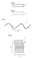
- wire saw 53 are wound on between guide rollers 51, 52 arranged with a predetermined interval therebetween.
- wire saw 53 is tensioned between guide rollers 51, 52, at a plurality of positions in each of guide rollers 51, 52, at predetermined intervals along a longitudinal direction of guide rollers 51, 52.
- guide rollers 51, 52 repeat forward rotation and reverse rotation, and thereby wire saw 53 reciprocates in a direction indicated by an arrow 55.
- semiconductor crystal ingot 50 While wire saw 53 is reciprocating in the direction indicated by arrow 55, semiconductor crystal ingot 50 is moved in a direction indicated by an arrow 54, and pressed against reciprocating wire saw 53. Thereby, as shown for example in the schematic perspective view of Fig. 2 , semiconductor crystal ingot 50 is cut at a plurality of positions, and a plurality of semiconductor substrates 1 are cut out.
- Fig. 3 shows a schematic cross sectional view of one example of wire saw 53 shown in Fig. 1 .
- wire saw 53 includes a core wire 53a, and abrasive grains 53b bonded on an outer peripheral surface of core wire 53a with a bond material (not shown).
- core wire 53a for example, a piano wire or the like can be used.
- abrasive grains 53b for example, diamond abrasive grains or the like can be used.
- the bond material for example, nickel or the like plated on the outer surface of core wire 53a can be used.
- Fig. 4 shows a schematic cross sectional view of one example of semiconductor substrate 1 obtained by cutting semiconductor crystal ingot 50 with wire saw 53.
- slice damage 1a is caused in surfaces of semiconductor substrate 1 by cutting semiconductor crystal ingot 50 with wire saw 53.
- semiconductor crystal ingot 50 for example, a crystal silicon ingot such as a single crystal silicon ingot or a polycrystalline silicon ingot fabricated by a Czochralski method or a casting method, or the like is used.
- a crystal silicon ingot is used as semiconductor crystal ingot 50, a silicon crystal substrate can be obtained as semiconductor substrate 1. It is noted that, in the present embodiment, semiconductor crystal ingot 50 has an n-type conductivity type by being doped with an n-type dopant.
- slice damage 1a in the surfaces of semiconductor substrate 1 shown in Fig. 4 is performed.
- slice damage 1a can be removed, for example, by etching with an alkaline aqueous solution such as an aqueous solution of sodium hydroxide or an aqueous solution of potassium hydroxide.
- semiconductor substrate 1 are not particularly limited, for example, a semiconductor substrate having a thickness of more than or equal to 100 ⁇ m and less than or equal to 300 ⁇ m, and having a surface in the shape of a rectangle with each side having a length of more than or equal to 100 mm and less than or equal to 200 mm, or the like can be used.
- Fig. 6 shows an enlarged schematic cross sectional view of one example of a portion of a surface of semiconductor substrate 1 shown in Fig. 5.
- Fig. 7 shows a schematic perspective view of one example of a portion of the surface of semiconductor substrate 1 shown in Fig. 5 .
- a large wave (indicated by an imaginary dash line in Fig. 6 ; hereinafter referred to as a "saw mark") 61 is formed, and abrasive grain marks 62 in the shape of grooves shallower than saw mark 61 are formed.
- Saw mark 61 is formed resulting from cutting of semiconductor crystal ingot 50 with wire saw 53. Specifically, when semiconductor substrate 1 is obtained by pressing semiconductor crystal ingot 50 against reciprocating wire saw 53 and cutting semiconductor crystal ingot 50 as shown in Fig. 1 , wire saw 53 is stopped momentarily each time when traveling direction 55 of wire saw 53 is switched, causing a reduction in the wire speed. This leads to different cutting depths into semiconductor crystal ingot 50 with wire saw 53 along the direction in which semiconductor crystal ingot 50 is moved with respect to wire saw 53 (i.e., direction indicated by arrow 54), which appear as saw mark 61 that is a large wave in the surface of semiconductor substrate 1.
- abrasive grain marks 62 are flaws formed by abrasive grains 53b of wire saw 53 during cutting of semiconductor crystal ingot 50 with wire saw 53, and are formed in the shape of grooves extending in traveling direction 55 of wire saw 53.
- crater-like depressions may be formed in the surface of semiconductor substrate 1 by the etching for removing slice damage 1 a described above.
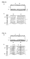
- an n-type doping paste 3 is placed on a portion of a surface on a back side (i.e., back surface) of semiconductor substrate 1.
- n-type doping paste 3 is placed to have a portion extending in a direction which forms an angle included in a range of -5° to +5° with a direction in which the abrasive grain marks (not shown) extend (i.e., direction indicated by arrow 55).
- n-type doping paste 3 when n-type doping paste 3 is placed to extend in the direction which forms an angle included in the range of -5° to +5° with the direction in which the abrasive grain marks extend, n-type doping paste 3 can be suppressed from flowing out in a direction other than the direction in which it extends, when compared with a case where n-type doping paste 3 is placed to extend in a direction outside the range.
- n-type doping paste 3 can be stably formed, at least in that portion, in the direction which forms an angle included in the range of -5° to +5° with the direction in which the abrasive grain marks extend (i.e., direction indicated by arrow 55). It is noted that, the present embodiment will describe a case where n-type doping paste 3 is formed in the shape of a band extending in a direction which forms an angle of 0° with the direction in which the abrasive grain marks extend (i.e., direction indicated by arrow 55).
- n-type doping paste 3 the one containing an n-type dopant such as a phosphorus compound, and also containing, for example, a solvent, a thickener, and a silicon oxide precursor can be used. Further, as n-type doping paste 3, the one not containing a thickener can also be used.
- phosphorus compound for example, a component containing phosphorus atoms such as phosphate, phosphorus oxide, phosphorus pentaoxide, phosphoric acid, or an organic phosphorus compound can be used alone or in combination of two or more kinds thereof.
- the solvent examples include ethylene glycol, methyl cellosolve, methyl cellosolve acetate, ethyl cellosolve, diethyl cellosolve, cellosolve acetate, ethylene glycol monophenyl ether, methoxyethanol, ethylene glycol monoacetate, ethylene glycol diacetate, diethylene glycol, diethylene glycol monomethyl ether, diethylene glycol monoethyl ether acetate, diethylene glycol monobutyl ether, diethylene glycol monobutyl ether acetate, diethylene glycol dimethyl ether, diethylene glycol methylethyl ether, diethylene glycol diethyl ether, diethylene glycol acetate, triethylglycol, triethylene glycol monomethyl ether, triethylene glycol monoethyl ether, tetraethylene glycol, liquid polyethylene glycol, propylene glycol, propylene glycol monomethyl ether, propylene glycol monoethyl ether, prop
- ethyl cellulose polyvinyl pyrrolidone, or a mixture thereof
- bentonite having various qualities and characteristics, a generally inorganic rheology additive for various polar solvent mixtures, nitrocellulose and other cellulose compounds, starch, gelatin, alginic acid, highly-dispersive amorphous silicic acid (Aerosil (registered trademark)), polyvinyl butyral (Mowital (registered trademark)), sodium carboxymethyl cellulose (vivistar), thermoplastic polyamide resin (Eurelon (registered trademark)), an organic castor oil derivative (Thixin R (registered trademark)), diamide wax (Thixatrol plus (registered trademark)), swelable polyacrylate (Rheolate (registered trademark)), polyether urea-polyurethane, polyether-polyol, or the like.
- the silicon oxide precursor for example, a substance represented by a general formula R 1' nSi(OR 1 ) 4-n (where R 1' represents methyl, ethyl, or phenyl, R 1 represents methyl, ethyl, n-propyl, or i-propyl, and n represents 0, 1, or 2) such as TEOS (tetraethyl orthosilicate) can be used.
- TEOS tetraethyl orthosilicate
- N-type doping paste 3 can be placed, for example, using a conventionally known technique such as screen printing, inkjet printing, or the like.
- n-type doping paste 3 placed on the back surface of semiconductor substrate 1 is dried.
- N-type doping paste 3 can be dried, for example, by placing semiconductor substrate 1 having the paste placed thereon inside an oven, and heating the paste at a temperature of, for example, about 200°C for a period of, for example, several tens of minutes.
- n-type dopant diffusion region 13 is formed in the shape of a band extending in a direction which forms an angle included in the range of -5° to +5° with the direction in which the abrasive grain marks extend (i.e., direction indicated by arrow 55). It is noted that n-type dopant diffusion region 13 is a region having an n-type dopant concentration higher than that in semiconductor substrate 1.
- n-type doping paste 3 on the back surface of silicon substrate 1 is removed.
- the residue of n-type doping paste 3 can be removed, for example, by immersing semiconductor substrate 1 having n-type doping paste 3 placed thereon in an aqueous solution of hydrofluoric acid, or the like.
- a p-type doping paste 4 is placed on a portion of the back surface of semiconductor substrate 1.
- p-type doping paste 4 is placed to have a portion extending in a direction which forms an angle included in a range of -5° to +5° with the direction in which the abrasive grain marks (not shown) extend (i.e., direction indicated by arrow 55), as with n-type doping paste 3 described above.
- p-type doping paste 4 the one containing a p-type dopant such as a boron compound, and also containing, for example, a solvent, a thickener, and a silicon oxide precursor can be used. Further, as p-type doping paste 4, the one not containing a thickener can also be used.
- boron compound for example, a compound containing boron atoms such as boron oxide, boric acid, an organic boron compound, or a boron-aluminum compound can be used alone or in combination of two or more kinds thereof.
- the same solvent as that in n-type doping paste 3 described above can be used.
- the same thickener as that in n-type doping paste 3 described above can be used.
- the silicon oxide precursor the same substance as that in n-type doping paste 3 described above can be used.
- P-type doping paste 4 can be placed using the same technique as that for placing n-type doping paste 3 described above.
- p-type doping paste 4 placed on the back surface of semiconductor substrate 1 is dried.
- P-type doping paste 4 can be dried using the same technique as that for drying n-type doping paste 3 described above.
- semiconductor substrate 1 is put into the quartz furnace at more than or equal to 800°C and less than or equal to 1100°C to diffuse the p-type dopant from p-type doping paste 4 into the back surface of semiconductor substrate 1, to form a p-type dopant diffusion region 14.
- p-type dopant diffusion region 14 is formed in the shape of a band extending in a direction which forms an angle included in the range of -5° to +5° with the direction in which the abrasive grain marks extend (i.e., direction indicated by arrow 55).
- a residue of p-type doping paste 4 on the back surface of silicon substrate 1 is removed.
- the residue of p-type doping paste 4 can be removed, for example, by immersing semiconductor substrate 1 having p-type doping paste 4 placed thereon in an aqueous solution of hydrofluoric acid, or the like.
- a passivation film 5 is formed on the back surface of semiconductor substrate 1.
- passivation film 5 for example, a silicon nitride film, a silicon oxide film, a laminated film of a silicon nitride film and a silicon oxide film, or the like can be used.
- Passivation film 5 can be formed, for example, by a plasma CVD method or the like.
- a texture structure 10 is formed by texture-etching a light receiving surface of semiconductor substrate 1 which is on a side opposite to a side having passivation film 5 formed thereon.
- the texture-etching for forming texture structure 10 can be performed by using passivation film 5 formed on the other surface of semiconductor substrate 1 as an etching mask.
- the texture-etching can be performed by etching the light receiving surface of semiconductor substrate 1 with an etching solution prepared for example by adding isopropyl alcohol to an aqueous solution of alkali such as sodium hydroxide or potassium hydroxide and heating the solution to, for example, more than or equal to 70°C and less than or equal to 80°C.
- an etching solution prepared for example by adding isopropyl alcohol to an aqueous solution of alkali such as sodium hydroxide or potassium hydroxide and heating the solution to, for example, more than or equal to 70°C and less than or equal to 80°C.
- a passivation film 6 is formed on the light receiving surface of semiconductor substrate 1.
- passivation film 6 for example, a silicon nitride film, a silicon oxide film, a laminated film of a silicon nitride film and a silicon oxide film, or the like can be used.
- Passivation film 6 can be formed, for example, by the plasma CVD method or the like.
- passivation film 6 on the light receiving surface of semiconductor substrate 1 is a film also serving as a so-called antireflection film.
- a contact hole 23 and a contact hole 24 are formed by removing portions of passivation film 5 on the back surface of semiconductor substrate 1 to expose a portion of n-type dopant diffusion region 13 from contact hole 23 and expose a portion of p-type dopant diffusion region 14 from contact hole 24.
- Contact holes 23, 24 can be formed, for example, by a method of forming a resist pattern having openings at portions corresponding to positions where contact holes 23, 24 are to be formed, on passivation film 5 using a photolithographic technique, and thereafter removing passivation film 5 from the openings in the resist pattern by etching.
- an electrode for n type 33 electrically connected to n-type dopant diffusion region 13 through contact hole 23 is formed, and an electrode for p type 34 electrically connected to p-type dopant diffusion region 14 through contact hole 24 is formed.
- electrode for n type 33 and electrode for p type 34 for example, an electrode made of a metal such as silver can be used.
- the back electrode type solar cell in the present embodiment can be fabricated.
- n-type doping paste 3 and p-type doping paste 4 are each placed to have a portion extending in the direction which forms an angle included in the range of -5° to +5° with the direction in which the abrasive grain marks extend as described above, n-type doping paste 3 and p-type doping paste 4 can be each formed to have a stable shape, at least in that portion, in the direction which forms an angle included in the range of -5° to +5° with the direction in which the abrasive grain marks extend.
- n-type dopant diffusion region 13 and p-type dopant diffusion region 14 can also be each formed stably in a desired shape, and thus the back electrode type solar cell can have good characteristics stably.
- the semiconductor crystal ingot may have a p-type conductivity type.
- n-type dopant diffusion region 13 and p-type dopant diffusion region 14 may each have a shape extending in one direction, as shown in the schematic plan view of Fig. 17 .
- a portion of at least one of n-type dopant diffusion region 13 and p-type dopant diffusion region 14 may be perpendicular to the direction in which the abrasive grain marks extend, as shown in the schematic plan view of Fig. 18 .
- only either n-type dopant diffusion region 13 or p-type dopant diffusion region 14 may have a shape extending in one direction, as shown in the schematic plan view of Fig. 19 .
- the present invention is not limited to a back electrode type solar cell, and is also applicable to semiconductor devices including a solar cell of any configuration such as a bifacial electrode type solar cell manufactured by forming electrodes on both a light receiving surface and a back surface of a semiconductor substrate.
- an n-type single crystal silicon ingot was pressed against a reciprocating wire saw (having a shape shown in the enlarged photograph of Fig. 20 ) and cut.
- a plurality of n-type single crystal silicon substrates each having a thickness of 200 ⁇ m were formed, in which abrasive grain marks in the shape of grooves extending in one direction were formed in a light receiving surface and a back surface in the shape of a quasi square with each side having a length of 126 mm.
- the wire saw shown in Fig. 20 used herein was fabricated by bonding diamond abrasive grains having a grain size of less than or equal to 30 ⁇ m, on an outer peripheral surface of a piano wire having a cross sectional diameter of 120 ⁇ m, with nickel plated thereon.
- Fig. 21 shows a microscope photograph of one example of a surface of an n-type single crystal silicon substrate cut with the wire saw described above
- Fig. 22 shows the result of measuring irregularities of the surface of the n-type single crystal silicon substrate shown in Fig. 21 with a laser microscope.
- the axis of abscissas in Fig. 22 represents the width of the surface of the n-type single crystal silicon substrate (maximum width: 10 mm)
- the axis of ordinates in Fig. 22 represents irregularities of the surface of the n-type single crystal silicon substrate caused by a saw mark and abrasive grain marks resulting from cutting with the wire saw.
- Fig. 23 shows a microscope photograph of another example of the surface of the n-type single crystal silicon substrate cut with the wire saw described above
- Fig. 24 shows the result of measuring irregularities of the surface of the n-type single crystal silicon substrate shown in Fig. 23 with a laser microscope.
- the axis of abscissas in Fig. 24 represents the width of the surface of the n-type single crystal silicon substrate (maximum width: 10 mm)
- the axis of ordinates in Fig. 24 represents irregularities of the surface of the n-type single crystal silicon substrate caused by a saw mark and abrasive grain marks resulting from cutting with the wire saw.
- slice damage in the surface of the n-type single crystal silicon substrate was removed by etching the surface of the n-type single crystal silicon substrate formed as described above, to a depth of 30 ⁇ m, with an aqueous solution of sodium hydroxide having a sodium hydroxide concentration of 48% by mass (i.e., 48 g of sodium hydroxide with respect to 52 g of water).
- Fig. 25 shows a microscope photograph of one example of the surface of the n-type single crystal silicon substrate shown in Fig. 21 subjected to etching
- Fig. 26 shows the result of measuring irregularities of the surface of the n-type single crystal silicon substrate shown in Fig. 25 with a laser microscope
- Fig. 27 shows the result of measuring irregularities of the surface of the n-type single crystal silicon substrate shown in Fig. 25 subjected to etching with a laser microscope.
- circular depressions were formed in the surface of the n-type single crystal silicon substrate as shown in Fig. 25 , the abrasive grain marks did not disappear from the surface of the n-type single crystal silicon substrate as shown in Figs. 26 and 27 .
- an n-type doping paste in the shape of a plurality of bands (design width of one band of the n-type doping paste: 300 ⁇ m, viscosity: 30 Pa ⁇ s) was placed intermittently at an interval of 1.5 mm to extend in a direction which formed an angle included in a range of -5° to +5° with a direction in which the abrasive grain marks extended.
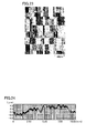
- Fig. 28(a) shows a microscope photograph of the surface of the n-type single crystal silicon substrate on which the n-type doping paste is placed to extend in the direction which forms an angle included in the range of -5° to +5° with the direction in which the abrasive grain marks extend
- Fig. 28(b) shows an enlarged photograph of the microscope photograph of Fig. 28(a) .
- a dark-colored portion is where the n-type doping paste is placed, and a light-colored portion indicates an opening.
- the n-type doping paste was placed as described above, except for placing the n-type doping paste in the shape of a plurality of bands to extend in a direction perpendicular to the direction in which the abrasive grain marks extended.
- Fig. 29(a) shows a microscope photograph of the surface of the n-type single crystal silicon substrate on which the n-type doping paste is placed to extend in the direction perpendicular to the direction in which the abrasive grain marks extend
- Fig. 29(b) shows an enlarged photograph of the microscope photograph of Fig. 29(a) .
- a dark-colored portion is where the n-type doping paste is placed, and a light-colored portion indicates an opening.
- any 10 n-type doping paste-placed portions (sample Nos. 1 to 10) were selected, the maximum value and the minimum value of the width of each of these 10 n-type doping paste-placed portions were measured, and the difference between the maximum value and the minimum value was calculated.
- any 10 n-type doping paste-placed portions were selected, the maximum value and the minimum value of the width of each of these 10 n-type doping paste-placed portions (sample Nos. 11 to 20) were measured, and the difference between the maximum value and the minimum value was calculated. Then, an average value and standard deviation ⁇ were calculated for each of the maximum values, the minimum values, and the differences between the maximum values and the minimum values, of the widths of the n-type doping paste-placed portions of sample Nos. 11 to 20. Table 2 shows results thereof.
- any 10 p-type doping paste-placed portions (sample Nos. 21 to 30) were selected, the maximum value and the minimum value of the width of each of these 10 p-type doping paste-placed portions were measured, and the difference between the maximum value and the minimum value was calculated.
- Table 3 shows results thereof.
- any 10 p-type doping paste-placed portions were selected, the maximum value and the minimum value of the width of each of these 10 p-type doping paste-placed portions (sample Nos. 31 to 40) were measured, and the difference between the maximum value and the minimum value was calculated.
- Table 4 shows results thereof.
- Back electrode type solar cells were fabricated, respectively using an n-type single crystal silicon substrate having n-type doping paste-placed portions of sample Nos. 1 to 10 and p-type doping paste-placed portions of sample Nos. 21 to 30 (i.e., a substrate of the Example), and an n-type single crystal silicon substrate having n-type doping paste-placed portions of sample Nos. 11 to 20 and p-type doping paste-placed portions of sample Nos. 31 to 40 (i.e., a substrate of the Comparative Example).
- an n-type doping paste was placed on each of the substrates of the Example and the Comparative Example thermally oxidized in a quartz furnace at 900°C for 20 minutes in an oxygen atmosphere. Thereafter, each of the substrates of the Example and the Comparative Example was placed inside an oven and heated at 200°C for 30 minutes to dry the n-type doping paste.
- each of the substrates of the Example and the Comparative Example was heated in the quartz furnace at 950°C for 30 minutes, and thereby phosphorus was diffused at the n-type doping paste-placed portions in each of the substrates of the Example and the Comparative Example to form n-type dopant diffusion regions.
- each of the substrates of the Example and the Comparative Example was immersed in an aqueous solution of hydrofluoric acid, thereby removing all of the residue of the n-type doping paste on each of the substrates of the Example and the Comparative Example.
- a p-type doping paste was placed between the n-type dopant diffusion regions formed in each of the substrates of the Example and the Comparative Example thermally oxidized in the quartz furnace at 900°C for 20 minutes in an oxygen atmosphere. Thereafter, each of the substrates of the Example and the Comparative Example was placed inside the oven and heated at 200°C for 30 minutes to dry the p-type doping paste.
- each of the substrates of the Example and the Comparative Example was heated in the quartz furnace at 1000°C for 30 minutes, and thereby boron was diffused at the p-type doping paste-placed portions in each of the substrates of the Example and the Comparative Example to form p-type dopant diffusion regions.
- each of the substrates of the Example and the Comparative Example was immersed in an aqueous solution of hydrofluoric acid, thereby removing all of the residue of the p-type doping paste on each of the substrates of the Example and the Comparative Example.
- a passivation film made of a silicon nitride film was formed by the plasma CVD method over the entire surface of each of the substrates of the Example and the Comparative Example on a side where the n-type dopant diffusion regions and the p-type dopant diffusion regions were formed.
- a texture structure was formed by texture-etching a surface of each of the substrates of the Example and the Comparative Example on a side opposite to the side having the passivation film formed thereon.
- the texture-etching was performed using an etching solution at 70°C to 80°C prepared by adding isopropyl alcohol to an aqueous solution of sodium hydroxide having a sodium hydroxide concentration of 3% by mass.
- an antireflection film made of a silicon nitride film was formed by the plasma CVD method on the texture structure of each of the substrates of the Example and the Comparative Example.
- contact holes were formed by removing portions of the passivation film on each of the substrates of the Example and the Comparative Example in the shape of bands to expose a portion of each of the n-type dopant diffusion regions and the p-type dopant diffusion regions.
- each of the back electrode type solar cell fabricated using the substrate of the Example (i.e., solar cell of the Example) and the back electrode type solar cell fabricated using the substrate of the Comparative Example (i.e., solar cell of the Comparative Example) was irradiated with quasi solar light using a solar simulator, and current-voltage (IV) characteristics were measured, and short circuit current density, open voltage, F. F (Fill Factor), conversion efficiency, and leak current were measured.
- Table 5 shows results thereof. It is noted that, in Table 5, values of the short circuit current density, open voltage, F. F, conversion efficiency, and leak current of the solar cell of the Example are expressed as relative values obtained when values of the short circuit current density, open voltage, F. F, conversion efficiency, and leak current of the solar cell of the Comparative Example are each set to 100. [Table 5] Short Circuit Current Density Open Voltage F.F Conversion Efficiency Leak Current Example 104 101 109 115 9 Comparative Example 100 100 100 100 100 100 100 100 100 100 100 100 100 100 100 100 100 100 100
- the solar cell of the Example has higher short circuit current density, open voltage, F. F, conversion efficiency, and lower leak current, when compared with the solar cell of the Comparative Example. Therefore, the solar cell of the Example can stably obtain good characteristics, when compared with the solar cell of the Comparative Example.
- each of the n-type dopant diffusion regions and the p-type dopant diffusion regions has less variation in width, when compared with the solar cell of the Comparative Example.
- the present invention is applicable to a semiconductor device and a method for manufacturing a semiconductor device, and in particular suitably applicable to a back electrode type solar cell and a method for manufacturing a back electrode type solar cell.
Landscapes
- Engineering & Computer Science (AREA)
- Mechanical Engineering (AREA)
- Photovoltaic Devices (AREA)
- Manufacturing & Machinery (AREA)
- Life Sciences & Earth Sciences (AREA)
- Sustainable Development (AREA)
- Sustainable Energy (AREA)
Abstract
Description
- The present invention relates to a semiconductor device and a method for manufacturing a semiconductor device.
- In recent years, development of clean energy has been desired due to the problem of exhaustion of energy resources, global environmental problems such as an increase in CO2 in the atmosphere, and the like, and photovoltaic power generation using solar cells in particular among semiconductor devices has been developed, put to practical use, and is progressing as a new energy source.
- As a solar cell, a bifacial electrode type solar cell has been conventionally a mainstream, in which a p-n junction is formed for example by diffusing an impurity having a conductivity type opposite to that of a single crystal or polycrystalline silicon substrate, into a light receiving surface of the silicon substrate, and electrodes are respectively formed on the light receiving surface and a back surface opposite to the light receiving surface of the silicon substrate. Further, in the bifacial electrode type solar cell, it is also common to achieve higher output using a back surface field effect, by diffusing a high concentration of an impurity having the same conductivity type as that of the silicon substrate into the back surface of the silicon substrate.
- In addition, research and development have also been made for a back electrode type solar cell in which no electrode is formed on a light receiving surface of a silicon substrate and electrodes are formed only on a back surface of the silicon substrate (see, for example, PTD 1 (Japanese Patent Laying-Open No.
2006-156646 - Hereinafter, one example of a method for manufacturing a conventional back electrode type solar cell will be described with reference to the schematic cross sectional views of
Figs. 30(a) to 30(i) . - First, as shown in
Fig. 30(a) , an n-type doping paste 103 is applied on a back surface of asilicon substrate 101 having an n-type or p-type conductivity type, and dried. N-type doping paste 103 is pattern-applied to follow the desired shape of an n-type dopant diffusion region. - Here, as
silicon substrate 101, for example, a silicon substrate obtained by slicing a silicon ingot can be used. Further, assilicon substrate 101, it is desirable to use a silicon substrate from which a slice damage layer caused by slicing has been removed. It is noted that the slice damage layer can be removed, for example, by etching with a mixed acid of an aqueous solution of hydrogen fluoride and nitric acid. - It is noted that the surface having n-
type doping paste 103 applied thereon is described here as the back surface ofsilicon substrate 101, and the other surface ofsilicon substrate 101 serves as a light receiving surface of the solar cell. Hereinafter, the light receiving surface may be referred to as a front surface. - Next, as shown in
Fig. 30(b) , an n-type dopant is diffused from n-type doping paste 103 intosemiconductor substrate 101 to form an n-typedopant diffusion region 113. Thereafter, a residue of n-type doping paste 103 on the back surface ofsilicon substrate 101 is removed with an aqueous solution of hydrogen fluoride. - Next, as shown in
Fig. 30(c) , a p-type doping paste 104 is pattern-applied on the back surface ofsilicon substrate 101 to follow the desired shape of a p-type dopant diffusion region, and dried. - Next, as shown in
Fig. 30(d) , a p-type dopant is diffused from p-type doping paste 104 intosilicon substrate 101 to form a p-typedopant diffusion region 114, and a residue of p-type doping paste 104 is removed with an aqueous solution of hydrogen fluoride. - Next, as shown in
Fig. 30(e) , asilicon oxide film 105 is formed on the back surface ofsilicon substrate 101 using a CVD method. On this occasion, a silicon nitride film, or a laminated film of a silicon oxide film and a silicon nitride film may be used instead ofsilicon oxide film 105. - Next, as shown in
Fig. 30(f) , atexture structure 110 is formed in the front surface ofsilicon substrate 101, using for example a mixed acid of an aqueous solution of hydrogen fluoride and nitric acid, or the like. It is noted that, on this occasion,silicon oxide film 105 on the back surface ofsilicon substrate 101 serves as a protective mask whentexture structure 110 is formed, and also serves as a passivation film on the back surface ofsilicon substrate 101. - Next, as shown in
Fig. 30(g) , a light receivingsurface passivation film 106 is formed on the front surface ofsilicon substrate 101 using the CVD method. As light receivingsurface passivation film 106, a silicon oxide film, a silicon nitride film, or a laminated film of a silicon oxide film and a silicon nitride film may be used. Further, light receivingsurface passivation film 106 is a film also serving as a so-called antireflection film. - Next, as shown in
Fig. 30(h) , portions ofsilicon oxide film 105 are removed to formcontact holes - Next, as shown in
Fig. 30(i) , an electrode forn type 133 electrically connected to n-typedopant diffusion region 113 throughcontact hole 123 is formed, and an electrode forp type 134 electrically connected to p-typedopant diffusion region 114 throughcontact hole 124 is formed. - Electrode for
n type 133 and electrode forp type 134 can be formed, for example, by printing a known metal paste by a screen printing method and firing the metal paste. - PTD 1: Japanese Patent Laying-Open No.
2006-156646 - However, the conventional back electrode type solar cell has a problem that n-type
dopant diffusion region 113 and p-typedopant diffusion region 114 cannot be formed at predetermined regions, respectively, and good characteristics cannot be obtained stably. - Such a problem occurs not only in the back electrode type solar cell, but also in all semiconductor devices including a solar cell such as a bifacial electrode type solar cell.
- In view of the above circumstances, one object of the present invention is to provide a semiconductor device and a method for manufacturing a semiconductor device capable of stably obtaining good characteristics.
- The present invention is directed to a semiconductor device including a semiconductor substrate, and a dopant diffusion region provided in one surface of the semiconductor substrate, wherein abrasive grain marks are formed in the surface of the semiconductor substrate, the dopant diffusion region has a portion extending in a direction which forms an angle included in a range of -5° to +5° with a direction in which the abrasive grain marks extend, and the dopant diffusion region is formed by diffusing a dopant from a doping paste placed on the one surface of the semiconductor substrate.
- Preferably, in the semiconductor device in accordance with the present invention, the dopant diffusion region has at least one of an n-type dopant diffusion region and a p-type dopant diffusion region, and the semiconductor device further includes an electrode for n type provided on the n-type dopant diffusion region, and an electrode for p type provided on the p-type dopant diffusion region.
- Further, the present invention is directed to a method for manufacturing a semiconductor device, including the steps of forming abrasive grain marks extending in one direction in a surface of a semiconductor substrate, placing a doping paste having a portion extending in a direction which forms an angle included in a range of -5' to +5° with a direction in which the abrasive grain marks extend, on a portion of the surface of the semiconductor substrate, and forming a dopant diffusion region from a dopant in the doping paste on the semiconductor substrate.
- Preferably, in the method for manufacturing a semiconductor device in accordance with the present invention, the step of forming the abrasive grain marks includes the step of cutting a semiconductor crystal ingot with a wire saw.
- Further, preferably, the method for manufacturing a semiconductor device in accordance with the present invention includes the step of etching the surface of the semiconductor substrate between the step of forming the abrasive grain marks and the step of placing the doping paste.
- According to the present invention, a semiconductor device and a method for manufacturing a semiconductor device capable of stably obtaining good characteristics can be provided.
-
-
Fig. 1 is a schematic perspective view illustrating one example of the step of cutting a semiconductor crystal ingot with a wire saw. -
Fig. 2 is a schematic perspective view illustrating one example of the step of cutting the semiconductor crystal ingot at a plurality of positions to cut out a plurality of semiconductor substrates. -
Fig. 3 is a schematic cross sectional view of one example of the wire saw shown inFig. 1 . -
Fig. 4 is a schematic cross sectional view of one example of a semiconductor substrate obtained by cutting the semiconductor crystal ingot with the wire saw shown inFig. 1 . -
Fig. 5 is a schematic cross sectional view illustrating one example of the step of removing slice damage in surfaces of the semiconductor substrate shown inFig. 4 . -
Fig. 6 is an enlarged schematic cross sectional view of one example of a portion of a surface of the semiconductor substrate shown inFig. 5 . -
Fig. 7 is a schematic perspective view of one example of a portion of the surface of the semiconductor substrate shown inFig. 5 . -
Fig. 8(a) is a schematic cross sectional view illustrating one example of the step of placing an n-type doping paste on a back surface of the semiconductor substrate, andFig. 8(b) is a schematic plan view illustrating one example of the step of placing the n-type doping paste on the back surface of the semiconductor substrate. -
Fig. 9(a) is a schematic cross sectional view illustrating one example of the step of forming an n-type dopant diffusion region in the back surface of the semiconductor substrate, andFig. 9(b) is a schematic plan view illustrating one example of the step of forming the n-type dopant diffusion region in the back surface of the semiconductor substrate. -
Fig. 10(a) is a schematic cross sectional view illustrating one example of the step of placing a p-type doping paste on the back surface of the semiconductor substrate, andFig. 10(b) is a schematic plan view illustrating one example of the step of placing the p-type doping paste on the back surface of the semiconductor substrate. -
Fig. 11(a) is a schematic cross sectional view illustrating one example of the step of forming a p-type dopant diffusion region in the back surface of the semiconductor substrate, andFig. 11 (b) is a schematic plan view illustrating one example of the step of forming the p-type dopant diffusion region in the back surface of the semiconductor substrate. -
Fig. 12(a) is a schematic cross sectional view illustrating one example of the step of forming a passivation film on the back surface of the semiconductor substrate, andFig. 12(b) is a schematic plan view illustrating one example of the step of forming the passivation film on the back surface of the semiconductor substrate. -
Fig. 13(a) is a schematic cross sectional view illustrating one example of the step of forming a texture structure in a front surface of the semiconductor substrate, andFig. 13(b) is a schematic plan view illustrating one example of the step of forming the texture structure in the front surface of the semiconductor substrate. -
Fig. 14(a) is a schematic cross sectional view illustrating one example of the step of forming a passivation film on the front surface of the semiconductor substrate, andFig. 14(b) is a schematic plan view illustrating one example of the step of forming the passivation film on the front surface of the semiconductor substrate. -
Fig. 15(a) is a schematic cross sectional view illustrating one example of the step of forming contact holes by removing portions of the passivation film on the back surface of the semiconductor substrate, andFig. 15(b) is a schematic plan view illustrating one example of the step of forming the contact holes by removing portions of the passivation film on the back surface of the semiconductor substrate. -
Fig. 16(a) is a schematic cross sectional view illustrating one example of the step of forming an electrode for n type and an electrode for p type, andFig. 16(b) is a schematic plan view illustrating one example of the step of forming the electrode for n type and the electrode for p type. -
Fig. 17 is a schematic plan view of one example of the n-type dopant diffusion region and the p-type dopant diffusion region formed in the back surface of the semiconductor substrate. -
Fig. 18 is a schematic plan view of another example of the n-type dopant diffusion region and the p-type dopant diffusion region formed in the back surface of the semiconductor substrate. -
Fig. 19 is a schematic plan view of another example of the n-type dopant diffusion region and the p-type dopant diffusion region formed in the back surface of the semiconductor substrate. -
Fig. 20 is an enlarged photograph of a wire saw used in an Example. -
Fig. 21 is a microscope photograph of one example of a surface of an n-type single crystal silicon substrate cut with the wire saw shown inFig. 20 . -
Fig. 22 is a view showing the result of measuring irregularities of the surface of the n-type single crystal silicon substrate shown inFig. 21 with a laser microscope. -
Fig. 23 is a microscope photograph of another example of the surface of the n-type single crystal silicon substrate cut with the wire saw shown inFig. 22 . -
Fig. 24 is a view showing the result of measuring irregularities of the surface of the n-type single crystal silicon substrate shown inFig. 23 with a laser microscope. -
Fig. 25 is a microscope photograph of one example of the surface of the n-type single crystal silicon substrate shown inFig. 21 subjected to etching. -
Fig. 26 is a view showing the result of measuring irregularities of the surface of the n-type single crystal silicon substrate shown inFig. 25 with a laser microscope. -
Fig. 27 is a view showing the result of measuring irregularities of the surface of the n-type single crystal silicon substrate shown inFig. 25 subjected to etching with a laser microscope. -
Fig. 28(a) is a microscope photograph of the surface of the n-type single crystal silicon substrate on which the n-type doping paste is placed to extend in a direction which forms an angle included in a range of -5° to +5° with a direction in which abrasive grain marks extend, andFig. 28(b) is an enlarged photograph of the microscope photograph ofFig. 28(a) . -
Fig. 29(a) is a microscope photograph of the surface of the n-type single crystal silicon substrate on which the n-type doping paste is placed to extend in a direction perpendicular to the direction in which the abrasive grain marks extend, andFig. 29(b) is an enlarged photograph of the microscope photograph ofFig. 29(a) . -
Figs. 30(a) to 30(i) are schematic cross sectional views illustrating one example of a method for manufacturing a conventional back electrode type solar cell. - Hereinafter, a method for manufacturing a back electrode type solar cell in accordance with an embodiment as one example of a method for manufacturing a semiconductor device in accordance with the present invention will be described with reference to
Figs.1 to 16 . It is noted that, in the drawings of the present invention, the same reference numerals designate identical or corresponding parts. - First, as shown in the schematic perspective view of
Fig. 1 , the step of cutting asemiconductor crystal ingot 50 with a wire saw 53 is performed. As shown inFig. 1 , wire saw 53 are wound on betweenguide rollers guide rollers guide rollers guide rollers rollers arrow 55. - While wire saw 53 is reciprocating in the direction indicated by
arrow 55,semiconductor crystal ingot 50 is moved in a direction indicated by anarrow 54, and pressed against reciprocating wire saw 53. Thereby, as shown for example in the schematic perspective view ofFig. 2 ,semiconductor crystal ingot 50 is cut at a plurality of positions, and a plurality ofsemiconductor substrates 1 are cut out. -
Fig. 3 shows a schematic cross sectional view of one example of wire saw 53 shown inFig. 1 . Here, wire saw 53 includes acore wire 53a, andabrasive grains 53b bonded on an outer peripheral surface ofcore wire 53a with a bond material (not shown). Ascore wire 53a, for example, a piano wire or the like can be used. Asabrasive grains 53b, for example, diamond abrasive grains or the like can be used. As the bond material, for example, nickel or the like plated on the outer surface ofcore wire 53a can be used. -
Fig. 4 shows a schematic cross sectional view of one example ofsemiconductor substrate 1 obtained by cuttingsemiconductor crystal ingot 50 with wire saw 53. Here,slice damage 1a is caused in surfaces ofsemiconductor substrate 1 by cuttingsemiconductor crystal ingot 50 with wire saw 53. - As
semiconductor crystal ingot 50, for example, a crystal silicon ingot such as a single crystal silicon ingot or a polycrystalline silicon ingot fabricated by a Czochralski method or a casting method, or the like is used. When a crystal silicon ingot is used assemiconductor crystal ingot 50, a silicon crystal substrate can be obtained assemiconductor substrate 1. It is noted that, in the present embodiment,semiconductor crystal ingot 50 has an n-type conductivity type by being doped with an n-type dopant. - Next, as shown in the schematic cross sectional view of
Fig. 5 , the step of removingslice damage 1a in the surfaces ofsemiconductor substrate 1 shown inFig. 4 is performed. Here, when a silicon crystal substrate is used assemiconductor substrate 1,slice damage 1a can be removed, for example, by etching with an alkaline aqueous solution such as an aqueous solution of sodium hydroxide or an aqueous solution of potassium hydroxide. - Although the size and shape of
semiconductor substrate 1 are not particularly limited, for example, a semiconductor substrate having a thickness of more than or equal to 100 µm and less than or equal to 300 µm, and having a surface in the shape of a rectangle with each side having a length of more than or equal to 100 mm and less than or equal to 200 mm, or the like can be used. -
Fig. 6 shows an enlarged schematic cross sectional view of one example of a portion of a surface ofsemiconductor substrate 1 shown inFig. 5. Fig. 7 shows a schematic perspective view of one example of a portion of the surface ofsemiconductor substrate 1 shown inFig. 5 . Here, in the surface ofsemiconductor substrate 1, a large wave (indicated by an imaginary dash line inFig. 6 ; hereinafter referred to as a "saw mark") 61 is formed, and abrasive grain marks 62 in the shape of grooves shallower thansaw mark 61 are formed. -
Saw mark 61 is formed resulting from cutting ofsemiconductor crystal ingot 50 with wire saw 53. Specifically, whensemiconductor substrate 1 is obtained by pressingsemiconductor crystal ingot 50 against reciprocating wire saw 53 and cuttingsemiconductor crystal ingot 50 as shown inFig. 1 , wire saw 53 is stopped momentarily each time when travelingdirection 55 of wire saw 53 is switched, causing a reduction in the wire speed. This leads to different cutting depths intosemiconductor crystal ingot 50 with wire saw 53 along the direction in whichsemiconductor crystal ingot 50 is moved with respect to wire saw 53 (i.e., direction indicated by arrow 54), which appear assaw mark 61 that is a large wave in the surface ofsemiconductor substrate 1. - In addition, abrasive grain marks 62 are flaws formed by
abrasive grains 53b of wire saw 53 during cutting ofsemiconductor crystal ingot 50 with wire saw 53, and are formed in the shape of grooves extending in travelingdirection 55 of wire saw 53. - It is noted that, although not shown in
Figs. 6 and 7 for convenience of explanation, crater-like depressions may be formed in the surface ofsemiconductor substrate 1 by the etching for removingslice damage 1 a described above. - Next, as shown in the schematic cross sectional view of
Fig. 8(a) and the schematic plan view ofFig. 8(b) , an n-type doping paste 3 is placed on a portion of a surface on a back side (i.e., back surface) ofsemiconductor substrate 1. - Here, as shown in the schematic plan view of
Fig. 8(b) , n-type doping paste 3 is placed to have a portion extending in a direction which forms an angle included in a range of -5° to +5° with a direction in which the abrasive grain marks (not shown) extend (i.e., direction indicated by arrow 55). This is based on the findings obtained by the inventor of the present invention through earnest study that, when n-type doping paste 3 is placed to extend in the direction which forms an angle included in the range of -5° to +5° with the direction in which the abrasive grain marks extend, n-type doping paste 3 can be suppressed from flowing out in a direction other than the direction in which it extends, when compared with a case where n-type doping paste 3 is placed to extend in a direction outside the range. Thereby, n-type doping paste 3 can be stably formed, at least in that portion, in the direction which forms an angle included in the range of -5° to +5° with the direction in which the abrasive grain marks extend (i.e., direction indicated by arrow 55). It is noted that, the present embodiment will describe a case where n-type doping paste 3 is formed in the shape of a band extending in a direction which forms an angle of 0° with the direction in which the abrasive grain marks extend (i.e., direction indicated by arrow 55). - As n-
type doping paste 3, the one containing an n-type dopant such as a phosphorus compound, and also containing, for example, a solvent, a thickener, and a silicon oxide precursor can be used. Further, as n-type doping paste 3, the one not containing a thickener can also be used. - As the phosphorus compound, for example, a component containing phosphorus atoms such as phosphate, phosphorus oxide, phosphorus pentaoxide, phosphoric acid, or an organic phosphorus compound can be used alone or in combination of two or more kinds thereof.
- Examples of the solvent include ethylene glycol, methyl cellosolve, methyl cellosolve acetate, ethyl cellosolve, diethyl cellosolve, cellosolve acetate, ethylene glycol monophenyl ether, methoxyethanol, ethylene glycol monoacetate, ethylene glycol diacetate, diethylene glycol, diethylene glycol monomethyl ether, diethylene glycol monoethyl ether acetate, diethylene glycol monobutyl ether, diethylene glycol monobutyl ether acetate, diethylene glycol dimethyl ether, diethylene glycol methylethyl ether, diethylene glycol diethyl ether, diethylene glycol acetate, triethylglycol, triethylene glycol monomethyl ether, triethylene glycol monoethyl ether, tetraethylene glycol, liquid polyethylene glycol, propylene glycol, propylene glycol monomethyl ether, propylene glycol monoethyl ether, propylene glycol monobutyl ether, 1-butoxyethoxy propanol, dipropyl glycol, dipropylene glycol monomethyl ether, dipropylene glycol monoethyl ether, tripropylene glycol monomethyl ether, polypropylene glycol, trimethylene glycol, butanedial, 1,5-pentanedial, hexylene glycol, glycerin, glyceryl acetate, glycerin diacetate, glyceryl triacetate, trimethylolpropine, 1,2,6-hexane triol, 1,2-propanediol, 1,5-pentanediol, octanediol, 1,2-butanediol, 1,4-butanediol, 1,3-butanediol, dioxane, trioxane, tetrahydrofuran, tetrahydropyran, methylal, diethyl acetal, methyl ethyl ketone, methyl isobutyl ketone, diethyl ketone, acetonylacetone, diacetone alcohol, methyl formate, ethyl formate, propyl formate, methyl acetate, and ethyl acetate, which can be used alone or in combination of two or more kinds thereof.
- As the thickener, although it is desirable to use ethyl cellulose, polyvinyl pyrrolidone, or a mixture thereof, it is also possible to use bentonite having various qualities and characteristics, a generally inorganic rheology additive for various polar solvent mixtures, nitrocellulose and other cellulose compounds, starch, gelatin, alginic acid, highly-dispersive amorphous silicic acid (Aerosil (registered trademark)), polyvinyl butyral (Mowital (registered trademark)), sodium carboxymethyl cellulose (vivistar), thermoplastic polyamide resin (Eurelon (registered trademark)), an organic castor oil derivative (Thixin R (registered trademark)), diamide wax (Thixatrol plus (registered trademark)), swelable polyacrylate (Rheolate (registered trademark)), polyether urea-polyurethane, polyether-polyol, or the like.
- As the silicon oxide precursor, for example, a substance represented by a general formula R1'nSi(OR1)4-n (where R1' represents methyl, ethyl, or phenyl, R1 represents methyl, ethyl, n-propyl, or i-propyl, and n represents 0, 1, or 2) such as TEOS (tetraethyl orthosilicate) can be used.
- N-
type doping paste 3 can be placed, for example, using a conventionally known technique such as screen printing, inkjet printing, or the like. - Thereafter, n-
type doping paste 3 placed on the back surface ofsemiconductor substrate 1 is dried. - N-
type doping paste 3 can be dried, for example, by placingsemiconductor substrate 1 having the paste placed thereon inside an oven, and heating the paste at a temperature of, for example, about 200°C for a period of, for example, several tens of minutes. - Next, as shown in the schematic cross sectional view of
Fig. 9(a) and the schematic plan view ofFig. 9(b) ,semiconductor substrate 1 is put into a quartz furnace at more than or equal to 800°C and less than or equal to 1100°C to diffuse the n-type dopant from n-type doping paste 3 into the back surface ofsemiconductor substrate 1, to form an n-typedopant diffusion region 13. Thereby, as shown in the schematic plan view ofFig. 9(b) , n-typedopant diffusion region 13 is formed in the shape of a band extending in a direction which forms an angle included in the range of -5° to +5° with the direction in which the abrasive grain marks extend (i.e., direction indicated by arrow 55). It is noted that n-typedopant diffusion region 13 is a region having an n-type dopant concentration higher than that insemiconductor substrate 1. - Thereafter, a residue of n-
type doping paste 3 on the back surface ofsilicon substrate 1 is removed. The residue of n-type doping paste 3 can be removed, for example, by immersingsemiconductor substrate 1 having n-type doping paste 3 placed thereon in an aqueous solution of hydrofluoric acid, or the like. - Next, as shown in the schematic cross sectional view of
Fig. 10(a) and the schematic plan view ofFig. 10(b) , a p-type doping paste 4 is placed on a portion of the back surface ofsemiconductor substrate 1. - Here, as shown in the schematic plan view of
Fig. 10(b) , p-type doping paste 4 is placed to have a portion extending in a direction which forms an angle included in a range of -5° to +5° with the direction in which the abrasive grain marks (not shown) extend (i.e., direction indicated by arrow 55), as with n-type doping paste 3 described above. - As p-
type doping paste 4, the one containing a p-type dopant such as a boron compound, and also containing, for example, a solvent, a thickener, and a silicon oxide precursor can be used. Further, as p-type doping paste 4, the one not containing a thickener can also be used. - As the boron compound, for example, a compound containing boron atoms such as boron oxide, boric acid, an organic boron compound, or a boron-aluminum compound can be used alone or in combination of two or more kinds thereof.
- As the solvent, the same solvent as that in n-
type doping paste 3 described above can be used. - As the thickener, the same thickener as that in n-
type doping paste 3 described above can be used. - As the silicon oxide precursor, the same substance as that in n-
type doping paste 3 described above can be used. - P-
type doping paste 4 can be placed using the same technique as that for placing n-type doping paste 3 described above. - Thereafter, p-
type doping paste 4 placed on the back surface ofsemiconductor substrate 1 is dried. - P-
type doping paste 4 can be dried using the same technique as that for drying n-type doping paste 3 described above. - Next, as shown in the schematic cross sectional view of
Fig. 11 (a) and the schematic plan view ofFig. 11(b) ,semiconductor substrate 1 is put into the quartz furnace at more than or equal to 800°C and less than or equal to 1100°C to diffuse the p-type dopant from p-type doping paste 4 into the back surface ofsemiconductor substrate 1, to form a p-typedopant diffusion region 14. Thereby, as shown in the schematic plan view ofFig. 11(b) , p-typedopant diffusion region 14 is formed in the shape of a band extending in a direction which forms an angle included in the range of -5° to +5° with the direction in which the abrasive grain marks extend (i.e., direction indicated by arrow 55). - Thereafter, a residue of p-
type doping paste 4 on the back surface ofsilicon substrate 1 is removed. The residue of p-type doping paste 4 can be removed, for example, by immersingsemiconductor substrate 1 having p-type doping paste 4 placed thereon in an aqueous solution of hydrofluoric acid, or the like. - Next, as shown in the schematic cross sectional view of
Fig. 12(a) and the schematic plan view ofFig. 12(b) , apassivation film 5 is formed on the back surface ofsemiconductor substrate 1. Aspassivation film 5, for example, a silicon nitride film, a silicon oxide film, a laminated film of a silicon nitride film and a silicon oxide film, or the like can be used.Passivation film 5 can be formed, for example, by a plasma CVD method or the like. - Next, as shown in the schematic cross sectional view of
Fig. 13(a) , atexture structure 10 is formed by texture-etching a light receiving surface ofsemiconductor substrate 1 which is on a side opposite to a side havingpassivation film 5 formed thereon. The texture-etching for formingtexture structure 10 can be performed by usingpassivation film 5 formed on the other surface ofsemiconductor substrate 1 as an etching mask. Whensemiconductor substrate 1 is made of a silicon crystal substrate, the texture-etching can be performed by etching the light receiving surface ofsemiconductor substrate 1 with an etching solution prepared for example by adding isopropyl alcohol to an aqueous solution of alkali such as sodium hydroxide or potassium hydroxide and heating the solution to, for example, more than or equal to 70°C and less than or equal to 80°C. - Next, as shown in the schematic cross sectional view of
Fig. 14(a) , apassivation film 6 is formed on the light receiving surface ofsemiconductor substrate 1. Aspassivation film 6, for example, a silicon nitride film, a silicon oxide film, a laminated film of a silicon nitride film and a silicon oxide film, or the like can be used.Passivation film 6 can be formed, for example, by the plasma CVD method or the like. Further,passivation film 6 on the light receiving surface ofsemiconductor substrate 1 is a film also serving as a so-called antireflection film. - Next, as shown in the schematic cross sectional view of
Fig. 15(a) and the schematic plan view ofFig. 15(b) , acontact hole 23 and acontact hole 24 are formed by removing portions ofpassivation film 5 on the back surface ofsemiconductor substrate 1 to expose a portion of n-typedopant diffusion region 13 fromcontact hole 23 and expose a portion of p-typedopant diffusion region 14 fromcontact hole 24. - Contact holes 23, 24 can be formed, for example, by a method of forming a resist pattern having openings at portions corresponding to positions where contact holes 23, 24 are to be formed, on
passivation film 5 using a photolithographic technique, and thereafter removingpassivation film 5 from the openings in the resist pattern by etching. - Next, as shown in the schematic cross sectional view of
Fig. 16(a) and the schematic plan view ofFig. 16(b) , an electrode forn type 33 electrically connected to n-typedopant diffusion region 13 throughcontact hole 23 is formed, and an electrode forp type 34 electrically connected to p-typedopant diffusion region 14 throughcontact hole 24 is formed. Here, as electrode forn type 33 and electrode forp type 34, for example, an electrode made of a metal such as silver can be used. Thus, the back electrode type solar cell in the present embodiment can be fabricated. - As described above, in the present embodiment, since n-
type doping paste 3 and p-type doping paste 4 are each placed to have a portion extending in the direction which forms an angle included in the range of -5° to +5° with the direction in which the abrasive grain marks extend as described above, n-type doping paste 3 and p-type doping paste 4 can be each formed to have a stable shape, at least in that portion, in the direction which forms an angle included in the range of -5° to +5° with the direction in which the abrasive grain marks extend. - Thereby, in the present embodiment, n-type
dopant diffusion region 13 and p-typedopant diffusion region 14 can also be each formed stably in a desired shape, and thus the back electrode type solar cell can have good characteristics stably. - It is noted that, although the above embodiment has described a semiconductor crystal ingot having an n-type conductivity type, the semiconductor crystal ingot may have a p-type conductivity type.
- Further, n-type
dopant diffusion region 13 and p-typedopant diffusion region 14 may each have a shape extending in one direction, as shown in the schematic plan view ofFig. 17 . Alternatively, a portion of at least one of n-typedopant diffusion region 13 and p-typedopant diffusion region 14 may be perpendicular to the direction in which the abrasive grain marks extend, as shown in the schematic plan view ofFig. 18 . Alternatively, only either n-typedopant diffusion region 13 or p-typedopant diffusion region 14 may have a shape extending in one direction, as shown in the schematic plan view ofFig. 19 . - Furthermore, the present invention is not limited to a back electrode type solar cell, and is also applicable to semiconductor devices including a solar cell of any configuration such as a bifacial electrode type solar cell manufactured by forming electrodes on both a light receiving surface and a back surface of a semiconductor substrate.
- First, an n-type single crystal silicon ingot was pressed against a reciprocating wire saw (having a shape shown in the enlarged photograph of
Fig. 20 ) and cut. Thereby, a plurality of n-type single crystal silicon substrates each having a thickness of 200 µm were formed, in which abrasive grain marks in the shape of grooves extending in one direction were formed in a light receiving surface and a back surface in the shape of a quasi square with each side having a length of 126 mm. The wire saw shown inFig. 20 used herein was fabricated by bonding diamond abrasive grains having a grain size of less than or equal to 30 µm, on an outer peripheral surface of a piano wire having a cross sectional diameter of 120 µm, with nickel plated thereon. -
Fig. 21 shows a microscope photograph of one example of a surface of an n-type single crystal silicon substrate cut with the wire saw described above, andFig. 22 shows the result of measuring irregularities of the surface of the n-type single crystal silicon substrate shown inFig. 21 with a laser microscope. It is noted that the axis of abscissas inFig. 22 represents the width of the surface of the n-type single crystal silicon substrate (maximum width: 10 mm), and the axis of ordinates inFig. 22 represents irregularities of the surface of the n-type single crystal silicon substrate caused by a saw mark and abrasive grain marks resulting from cutting with the wire saw. -
Fig. 23 shows a microscope photograph of another example of the surface of the n-type single crystal silicon substrate cut with the wire saw described above, andFig. 24 shows the result of measuring irregularities of the surface of the n-type single crystal silicon substrate shown inFig. 23 with a laser microscope. It is noted that the axis of abscissas inFig. 24 represents the width of the surface of the n-type single crystal silicon substrate (maximum width: 10 mm), and the axis of ordinates inFig. 24 represents irregularities of the surface of the n-type single crystal silicon substrate caused by a saw mark and abrasive grain marks resulting from cutting with the wire saw. - It was confirmed that, as shown in
Figs. 21 to 24 , a saw mark as a large wave formed along a direction in which the n-type single crystal silicon ingot was pressed against the wire saw, and abrasive grain marks in the shape of grooves formed in the saw mark along a traveling direction of the wire saw (vertical lines inFigs. 21 and23 ) were formed in the surface of the n-type single crystal silicon substrate. - Next, slice damage in the surface of the n-type single crystal silicon substrate was removed by etching the surface of the n-type single crystal silicon substrate formed as described above, to a depth of 30 µm, with an aqueous solution of sodium hydroxide having a sodium hydroxide concentration of 48% by mass (i.e., 48 g of sodium hydroxide with respect to 52 g of water).
-
Fig. 25 shows a microscope photograph of one example of the surface of the n-type single crystal silicon substrate shown inFig. 21 subjected to etching, andFig. 26 shows the result of measuring irregularities of the surface of the n-type single crystal silicon substrate shown inFig. 25 with a laser microscope.Fig. 27 shows the result of measuring irregularities of the surface of the n-type single crystal silicon substrate shown inFig. 25 subjected to etching with a laser microscope. Although circular depressions were formed in the surface of the n-type single crystal silicon substrate as shown inFig. 25 , the abrasive grain marks did not disappear from the surface of the n-type single crystal silicon substrate as shown inFigs. 26 and 27 . - Next, on the surface of the n-type single crystal silicon substrate subjected to etching described above, an n-type doping paste in the shape of a plurality of bands (design width of one band of the n-type doping paste: 300 µm, viscosity: 30 Pa·s) was placed intermittently at an interval of 1.5 mm to extend in a direction which formed an angle included in a range of -5° to +5° with a direction in which the abrasive grain marks extended.
-
Fig. 28(a) shows a microscope photograph of the surface of the n-type single crystal silicon substrate on which the n-type doping paste is placed to extend in the direction which forms an angle included in the range of -5° to +5° with the direction in which the abrasive grain marks extend, andFig. 28(b) shows an enlarged photograph of the microscope photograph ofFig. 28(a) . InFigs. 28(a) and 28(b) , a dark-colored portion is where the n-type doping paste is placed, and a light-colored portion indicates an opening. - It was confirmed that, as shown in
Figs. 28(a) and 28(b) , when the n-type doping paste was placed to extend in the direction which formed an angle included in the range of -5° to +5° with the direction in which the abrasive grain marks extended, the n-type doping paste was able to be suppressed from flowing out in a direction other than the direction in which the n-type doping paste extended. - As a Comparative Example, the n-type doping paste was placed as described above, except for placing the n-type doping paste in the shape of a plurality of bands to extend in a direction perpendicular to the direction in which the abrasive grain marks extended.
-
Fig. 29(a) shows a microscope photograph of the surface of the n-type single crystal silicon substrate on which the n-type doping paste is placed to extend in the direction perpendicular to the direction in which the abrasive grain marks extend, andFig. 29(b) shows an enlarged photograph of the microscope photograph ofFig. 29(a) . InFigs. 29(a) and 29(b) , a dark-colored portion is where the n-type doping paste is placed, and a light-colored portion indicates an opening. - It was confirmed that, as shown in
Figs. 29(a) and 29(b) , when the n-type doping paste was placed to extend in the direction perpendicular to the direction in which the abrasive grain marks extended, the n-type doping paste flew out in a direction other than the direction in which the n-type doping paste extended, and had a varied width, when compared with the case where the n-type doping paste was placed to extend in the direction which formed an angle included in the range of -5° to +5° with the direction in which the abrasive grain marks extended. - Further, from the surface of the n-type single crystal silicon substrate on which the n-type doping paste was placed to extend in the direction which formed an angle included in the range of -5° to +5° with the direction in which the abrasive grain marks extended, any 10 n-type doping paste-placed portions (sample Nos. 1 to 10) were selected, the maximum value and the minimum value of the width of each of these 10 n-type doping paste-placed portions were measured, and the difference between the maximum value and the minimum value was calculated. Then, an average value and a standard deviation σ were calculated for each of the maximum values, the minimum values, and the differences between the maximum values and the minimum values, of the widths of the n-type doping paste-placed portions of sample Nos. 1 to 10. Table 1 shows results thereof.
[Table 1] (n-type doping paste applied vertically*1) (unit: µm) Sample No. Maximum Width Minimum Width Maximum Width- Minimum Width 1 333 292 41 2 356 303 53 3 320 289 31 4 344 295 49 5 306 280 26 6 328 291 37 7 317 275 42 8 321 290 31 9 332 292 40 10 310 298 12 Average Value 327 291 36 σ 15 8 12 * 1: the n-type doping paste was placed to extend in the direction which formed an angle included in the range of -5° to +5° with the direction in which the abrasive grain marks extended - As shown in Table 1, for the maximum values, the minimum values, and the differences between the maximum values and the minimum values of the widths of the n-type doping paste-placed portions of sample Nos. 1 to 10, the average values were 327, 291, and 36, respectively, and standard deviations σ were 15, 8, and 12, respectively.
- In contrast, from the surface of the n-type single crystal silicon substrate on which the n-type doping paste was placed to extend in the direction perpendicular to the direction in which the abrasive grain marks extended, any 10 n-type doping paste-placed portions were selected, the maximum value and the minimum value of the width of each of these 10 n-type doping paste-placed portions (sample Nos. 11 to 20) were measured, and the difference between the maximum value and the minimum value was calculated. Then, an average value and standard deviation σ were calculated for each of the maximum values, the minimum values, and the differences between the maximum values and the minimum values, of the widths of the n-type doping paste-placed portions of sample Nos. 11 to 20. Table 2 shows results thereof.
[Table 2] (n-type doping paste applied laterally*2) (unit: µm) Sample No. Maximum Width Minimum Width Maximum Width-Minimum Width 11 381 300 81 12 356 288 68 13 375 293 82 14 374 290 84 15 396 275 121 16 428 305 123 17 396 292 104 18 361 292 69 19 388 294 94 20 403 303 100 Average Value 386 293 93 σ 21 9 19 *2: the doping paste was placed to extend in the direction perpendicular to the direction in which the abrasive grain marks extended - As shown in Table 2, for the maximum values, the minimum values, and the differences between the maximum values and the minimum values of the widths of the n-type doping paste-placed portions of sample Nos. 11 to 20, the average values were 386, 293, 93, respectively, and standard deviations σ were 21,9, and 19, respectively.
- Similarly, for a p-type doping paste, comparison was made between a case where the p-type doping paste was placed to extend in a direction which formed an angle included in a range of -5° to +5° with the direction in which the abrasive grain marks extended and a case where the p-type doping paste was placed to extend in a direction perpendicular to the direction in which the abrasive grain marks extended. The p-type doping paste in the shape of a plurality of bands was placed on the surface of the silicon substrate, intermittently at an interval of 1.5 mm (design width of one band of the p-type doping paste: 1000 µm, viscosity: 30 Pa·s)
- As with the n-type doping paste, from the surface of the n-type single crystal silicon substrate on which the p-type doping paste was placed to extend in the direction which formed an angle included in the range of -5° to +5° with the direction in which the abrasive grain marks extended, any 10 p-type doping paste-placed portions (sample Nos. 21 to 30) were selected, the maximum value and the minimum value of the width of each of these 10 p-type doping paste-placed portions were measured, and the difference between the maximum value and the minimum value was calculated. Table 3 shows results thereof.
- Further; as the Comparative Example, from the surface of the n-type single crystal silicon substrate on which the p-type doping paste was placed to extend in a direction perpendicular to the direction in which the abrasive grain marks extended, any 10 p-type doping paste-placed portions were selected, the maximum value and the minimum value of the width of each of these 10 p-type doping paste-placed portions (sample Nos. 31 to 40) were measured, and the difference between the maximum value and the minimum value was calculated. Table 4 shows results thereof.
- Furthermore, an average value and standard deviation σ were calculated for each of the maximum values, the minimum values, and the differences between the maximum values and the minimum values, of the widths of the p-type doping paste-placed portions of sample Nos. 21 to 30 and sample Nos. 31 to 40. Tables 3 and 4 show results thereof.
[Table 3] (p-type doping paste applied vertically* 1) (unit: µm) Sample No. Maximum Width Minimum Width Maximum Width-Minimum Width 21 1028 980 48 22 1009 967 42 23 1036 992 44 24 1020 970 50 25 1036 985 51 26 1031 992 39 27 1042 1001 41 28 1015 979 36 29 1029 977 52 30 1045 995 50 Average Value 1029 974 45 σ 12 11 6 * 1: the p-type doping paste was placed to extend in the direction which formed an angle included in the range of -5° to +5° with the direction in which the abrasive grain marks extended [Table 4] (p-type doping paste applied laterally*2) (unit: µm) Sample No. Maximum Width Minimum Width Maximum Width-Minimum Width 31 1088 977 111 32 1112 989 123 33 1140 991 149 34 1095 964 131 35 1124 997 127 36 1108 993 115 37 1099 981 118 38 1131 993 138 39 1154 1005 149 40 1129 980 149 Average Value 1118 987 131 σ 21 12 15 *2: the doping paste was placed to extend in the direction perpendicular to the direction in which the abrasive grain marks extended - As shown in Table 3, for the maximum values, the minimum values, and the differences between the maximum values and the minimum values of the widths of the p-type doping paste-placed portions of sample Nos. 21 to 30, the average values were 1029, 974, and 45, respectively, and standard deviations σ were 12, 11, and 6, respectively.
- Further, as shown in Table 4, for the maximum values, the minimum values, and the differences between the maximum values and the minimum values of the widths of the p-type doping paste-placed portions of sample Nos. 31 to 40, the average values were 1118, 987, and 131, respectively, and standard deviations σ were 21, 12, and 15, respectively.
- As described above, it was confirmed that, as shown in Tables 1 to 4, deviation of the width of the n-type doping paste from a designed value can be suppressed when the doping paste is placed to extend in the direction which forms an angle included in the range of -5° to +5° with the direction in which the abrasive grain marks extend, when compared with the case where the doping paste is placed to extend in the direction perpendicular to the direction in which the abrasive grain marks extend.
- Back electrode type solar cells were fabricated, respectively using an n-type single crystal silicon substrate having n-type doping paste-placed portions of sample Nos. 1 to 10 and p-type doping paste-placed portions of sample Nos. 21 to 30 (i.e., a substrate of the Example), and an n-type single crystal silicon substrate having n-type doping paste-placed portions of sample Nos. 11 to 20 and p-type doping paste-placed portions of sample Nos. 31 to 40 (i.e., a substrate of the Comparative Example).
- Specifically, first, an n-type doping paste was placed on each of the substrates of the Example and the Comparative Example thermally oxidized in a quartz furnace at 900°C for 20 minutes in an oxygen atmosphere. Thereafter, each of the substrates of the Example and the Comparative Example was placed inside an oven and heated at 200°C for 30 minutes to dry the n-type doping paste.
- Next, each of the substrates of the Example and the Comparative Example was heated in the quartz furnace at 950°C for 30 minutes, and thereby phosphorus was diffused at the n-type doping paste-placed portions in each of the substrates of the Example and the Comparative Example to form n-type dopant diffusion regions.
- Next, each of the substrates of the Example and the Comparative Example was immersed in an aqueous solution of hydrofluoric acid, thereby removing all of the residue of the n-type doping paste on each of the substrates of the Example and the Comparative Example.
- Next, a p-type doping paste was placed between the n-type dopant diffusion regions formed in each of the substrates of the Example and the Comparative Example thermally oxidized in the quartz furnace at 900°C for 20 minutes in an oxygen atmosphere. Thereafter, each of the substrates of the Example and the Comparative Example was placed inside the oven and heated at 200°C for 30 minutes to dry the p-type doping paste.
- Next, each of the substrates of the Example and the Comparative Example was heated in the quartz furnace at 1000°C for 30 minutes, and thereby boron was diffused at the p-type doping paste-placed portions in each of the substrates of the Example and the Comparative Example to form p-type dopant diffusion regions.
- Next, each of the substrates of the Example and the Comparative Example was immersed in an aqueous solution of hydrofluoric acid, thereby removing all of the residue of the p-type doping paste on each of the substrates of the Example and the Comparative Example.
- Next, a passivation film made of a silicon nitride film was formed by the plasma CVD method over the entire surface of each of the substrates of the Example and the Comparative Example on a side where the n-type dopant diffusion regions and the p-type dopant diffusion regions were formed.
- Next, a texture structure was formed by texture-etching a surface of each of the substrates of the Example and the Comparative Example on a side opposite to the side having the passivation film formed thereon. Here, the texture-etching was performed using an etching solution at 70°C to 80°C prepared by adding isopropyl alcohol to an aqueous solution of sodium hydroxide having a sodium hydroxide concentration of 3% by mass.
- Next, an antireflection film made of a silicon nitride film was formed by the plasma CVD method on the texture structure of each of the substrates of the Example and the Comparative Example.
- Next, contact holes were formed by removing portions of the passivation film on each of the substrates of the Example and the Comparative Example in the shape of bands to expose a portion of each of the n-type dopant diffusion regions and the p-type dopant diffusion regions.
- Thereafter, a commercially available silver paste was applied to fill the contact holes in each of the substrates of the Example and the Comparative Example, was dried, and fired by being heated at 600°C for 20 minutes, to form silver electrodes in contact with the n-type dopant diffusion regions and the p-type dopant diffusion regions, respectively. Thereby, the back electrode type solar cells respectively using the substrates of the Example and the Comparative Example were fabricated.
- Subsequently, each of the back electrode type solar cell fabricated using the substrate of the Example (i.e., solar cell of the Example) and the back electrode type solar cell fabricated using the substrate of the Comparative Example (i.e., solar cell of the Comparative Example) was irradiated with quasi solar light using a solar simulator, and current-voltage (IV) characteristics were measured, and short circuit current density, open voltage, F. F (Fill Factor), conversion efficiency, and leak current were measured. Table 5 shows results thereof. It is noted that, in Table 5, values of the short circuit current density, open voltage, F. F, conversion efficiency, and leak current of the solar cell of the Example are expressed as relative values obtained when values of the short circuit current density, open voltage, F. F, conversion efficiency, and leak current of the solar cell of the Comparative Example are each set to 100.
[Table 5] Short Circuit Current Density Open Voltage F.F Conversion Efficiency Leak Current Example 104 101 109 115 9 Comparative Example 100 100 100 100 100 - It was confirmed that, as shown in Table 5, the solar cell of the Example has higher short circuit current density, open voltage, F. F, conversion efficiency, and lower leak current, when compared with the solar cell of the Comparative Example. Therefore, the solar cell of the Example can stably obtain good characteristics, when compared with the solar cell of the Comparative Example.
- This is considered to be because, since the n-type dopant diffusion regions and the p-type dopant diffusion regions can be stably formed in the shape of bands extending in the direction which forms an angle included in the range of -5° to +5° with the direction in which the abrasive grain marks extend in the solar cell of the Example, each of the n-type dopant diffusion regions and the p-type dopant diffusion regions has less variation in width, when compared with the solar cell of the Comparative Example.
- It should be understood that the embodiment and the example disclosed herein are illustrative and non-restrictive in every respect. The scope of the present invention is defined by the scope of the claims, rather than the description above, and is intended to include any modifications within the scope and meaning equivalent to the scope of the claims.
- The present invention is applicable to a semiconductor device and a method for manufacturing a semiconductor device, and in particular suitably applicable to a back electrode type solar cell and a method for manufacturing a back electrode type solar cell.
- 1: semiconductor substrate; 1a: slice damage; 3: n-type doping paste; 4: p-type doping paste; 5: passivation film; 10: texture structure; 6: passivation film; 13: n-type dopant diffusion region; 14: p-type dopant diffusion region; 23, 24: contact hole; 33: electrode for n type; 34: electrode for p type; 50: semiconductor crystal ingot; 51, 52: guide roller; 53: wire saw; 53a: core wire; 53b: abrasive grains; 54, 55: arrow; 61: saw mark; 62: abrasive grain marks; 101: silicon substrate; 103: n-type doping paste; 104: p-type doping paste; 105: silicon oxide film; 106: light receiving surface passivation film; 110: texture structure; 113: n-type dopant diffusion region; 114: p-type dopant diffusion region; 123, 124: contact hole; 133: electrode for n type; 134: electrode for p type.
Claims (5)
- A semiconductor device, comprising:a semiconductor substrate; anda dopant diffusion region provided in one surface of said semiconductor substrate, whereinabrasive grain marks are formed in said surface of said semiconductor substrate,said dopant diffusion region has a portion extending in a direction which forms an angle included in a range of -5° to +5° with a direction in which said abrasive grain marks extend, andsaid dopant diffusion region is formed by diffusing a dopant from a doping paste placed on the one surface of said semiconductor substrate.
- The semiconductor device according to claim 1, wherein
said dopant diffusion region has at least one of an n-type dopant diffusion region and a p-type dopant diffusion region, and
the semiconductor device further comprises:an electrode for n type provided on said n-type dopant diffusion region; andan electrode for p type provided on said p-type dopant diffusion region. - A method for manufacturing a semiconductor device, comprising the steps of:forming abrasive grain marks extending in one direction in a surface of a semiconductor substrate;placing a doping paste having a portion extending in a direction which forms an angle included in a range of -5° to +5° with a direction in which said abrasive grain marks extend, on a portion of said surface of said semiconductor substrate; andforming a dopant diffusion region from a dopant in said doping paste on said semiconductor substrate.
- The method for manufacturing a semiconductor device according to claim 3, wherein said step of forming the abrasive grain marks includes the step of cutting a semiconductor crystal ingot with a wire saw.
- The method for manufacturing a semiconductor device according to claim 3 or 4, comprising the step of etching said surface of said semiconductor substrate between said step of forming the abrasive grain marks and said step of placing the doping paste.
Applications Claiming Priority (2)
| Application Number | Priority Date | Filing Date | Title |
|---|---|---|---|
| JP2011247307A JP5221738B2 (en) | 2011-11-11 | 2011-11-11 | Semiconductor device and manufacturing method of semiconductor device |
| PCT/JP2012/078816 WO2013069672A1 (en) | 2011-11-11 | 2012-11-07 | Semiconductor device and method for producing semiconductor device |
Publications (2)
| Publication Number | Publication Date |
|---|---|
| EP2779215A1 true EP2779215A1 (en) | 2014-09-17 |
| EP2779215A4 EP2779215A4 (en) | 2015-06-17 |
Family
ID=48290046
Family Applications (1)
| Application Number | Title | Priority Date | Filing Date |
|---|---|---|---|
| EP12848064.7A Withdrawn EP2779215A4 (en) | 2011-11-11 | 2012-11-07 | SEMICONDUCTOR DEVICE AND METHOD FOR MANUFACTURING SEMICONDUCTOR DEVICE |
Country Status (5)
| Country | Link |
|---|---|
| US (1) | US9214430B2 (en) |
| EP (1) | EP2779215A4 (en) |
| JP (1) | JP5221738B2 (en) |
| CN (1) | CN104040721A (en) |
| WO (1) | WO2013069672A1 (en) |
Families Citing this family (3)
| Publication number | Priority date | Publication date | Assignee | Title |
|---|---|---|---|---|
| US9117845B2 (en) * | 2013-01-25 | 2015-08-25 | Fairchild Semiconductor Corporation | Production of laterally diffused oxide semiconductor (LDMOS) device and a bipolar junction transistor (BJT) device using a semiconductor process |
| US10079319B2 (en) * | 2015-12-16 | 2018-09-18 | Sunpower Corporation | Solar cell fabrication using laser patterning of ion-implanted etch-resistant layers and the resulting solar cells |
| US11621168B1 (en) | 2022-07-12 | 2023-04-04 | Gyrotron Technology, Inc. | Method and system for doping semiconductor materials |
Family Cites Families (10)
| Publication number | Priority date | Publication date | Assignee | Title |
|---|---|---|---|---|
| JP2005310830A (en) * | 2004-04-16 | 2005-11-04 | Sharp Corp | Solar cell and method for manufacturing solar cell |
| JP2006156646A (en) | 2004-11-29 | 2006-06-15 | Sharp Corp | Manufacturing method of solar cell |
| WO2009041266A1 (en) * | 2007-09-28 | 2009-04-02 | Sharp Kabushiki Kaisha | Solar cell wafer manufacturing method |
| JP4998241B2 (en) * | 2007-12-11 | 2012-08-15 | 信越半導体株式会社 | Method of cutting workpiece by wire saw and wire saw |
| JP5003696B2 (en) * | 2009-02-04 | 2012-08-15 | 住友電気工業株式会社 | Group III nitride substrate and manufacturing method thereof |
| JP2010205839A (en) * | 2009-03-02 | 2010-09-16 | Sharp Corp | Method of manufacturing semiconductor device |
| JP2012230929A (en) * | 2009-08-28 | 2012-11-22 | Sumco Corp | Solar cell silicon wafer and manufacturing method thereof |
| JP4831709B2 (en) | 2010-05-21 | 2011-12-07 | シャープ株式会社 | Semiconductor device and manufacturing method of semiconductor device |
| JP2013012668A (en) * | 2011-06-30 | 2013-01-17 | Sharp Corp | Wafer for solar cell, solar cell and method for manufacturing the same |
| JP2013012667A (en) * | 2011-06-30 | 2013-01-17 | Sharp Corp | Wafer for solar cell, solar cell and method for manufacturing the same |
-
2011
- 2011-11-11 JP JP2011247307A patent/JP5221738B2/en active Active
-
2012
- 2012-11-07 WO PCT/JP2012/078816 patent/WO2013069672A1/en not_active Ceased
- 2012-11-07 EP EP12848064.7A patent/EP2779215A4/en not_active Withdrawn
- 2012-11-07 CN CN201280066800.2A patent/CN104040721A/en active Pending
- 2012-11-07 US US14/357,649 patent/US9214430B2/en not_active Expired - Fee Related
Also Published As
| Publication number | Publication date |
|---|---|
| EP2779215A4 (en) | 2015-06-17 |
| JP2013105818A (en) | 2013-05-30 |
| US9214430B2 (en) | 2015-12-15 |
| WO2013069672A1 (en) | 2013-05-16 |
| US20140339682A1 (en) | 2014-11-20 |
| CN104040721A (en) | 2014-09-10 |
| JP5221738B2 (en) | 2013-06-26 |
Similar Documents
| Publication | Publication Date | Title |
|---|---|---|
| US9178086B2 (en) | Method for fabricating back-contact type solar cell | |
| US7705236B2 (en) | Electrode material, solar cell, and method for producing solar cell | |
| US20100032012A1 (en) | Solar cell and method of manufacturing the same | |
| EP2405486A1 (en) | Process for producing semiconductor device | |
| WO2013002060A1 (en) | Wafer for solar cell, solar cell, and production method therefor | |
| US20110298100A1 (en) | Semiconductor device producing method and semiconductor device | |
| KR20130036258A (en) | Selective emitter solar cells formed by a hybrid diffusion and ion implantation process | |
| EP2584611A1 (en) | Silicon wafer, semiconductor device, silicon wafer production method and semiconductor device production method | |
| EP2779215A1 (en) | Semiconductor device and method for producing semiconductor device | |
| WO2010110106A1 (en) | Method of producing photoelectric conversion element, and photoelectric conversion element | |
| EP2573822B1 (en) | Semiconductor device, and method for producing semiconductor device | |
| JP2010205965A (en) | Method for manufacturing semiconductor device | |
| JP2008244282A (en) | Photoelectric conversion element and manufacturing method thereof | |
| JP2013012668A (en) | Wafer for solar cell, solar cell and method for manufacturing the same | |
| KR20120134141A (en) | Method for producing semiconductor device | |
| JP2016139762A (en) | Method for manufacturing solar cell element | |
| CN104521002A (en) | Manufacturing method of solar cell | |
| JP2015228416A (en) | Manufacturing method of solar cell | |
| JP6502651B2 (en) | Method of manufacturing solar cell and method of manufacturing solar cell module | |
| EP3217437B1 (en) | Solar cell and method for manufacturing same |
Legal Events
| Date | Code | Title | Description |
|---|---|---|---|
| PUAI | Public reference made under article 153(3) epc to a published international application that has entered the european phase |
Free format text: ORIGINAL CODE: 0009012 |
|
| 17P | Request for examination filed |
Effective date: 20140519 |
|
| AK | Designated contracting states |
Kind code of ref document: A1 Designated state(s): AL AT BE BG CH CY CZ DE DK EE ES FI FR GB GR HR HU IE IS IT LI LT LU LV MC MK MT NL NO PL PT RO RS SE SI SK SM TR |
|
| RIN1 | Information on inventor provided before grant (corrected) |
Inventor name: FUNAKOSHI, YASUSHI |
|
| DAX | Request for extension of the european patent (deleted) | ||
| RA4 | Supplementary search report drawn up and despatched (corrected) |
Effective date: 20150518 |
|
| RIC1 | Information provided on ipc code assigned before grant |
Ipc: B28D 5/04 20060101ALI20150511BHEP Ipc: H01L 23/544 20060101ALI20150511BHEP Ipc: H01L 31/18 20060101ALI20150511BHEP Ipc: H01L 31/068 20120101AFI20150511BHEP Ipc: H01L 21/225 20060101ALI20150511BHEP Ipc: B24B 27/06 20060101ALI20150511BHEP Ipc: H01L 21/304 20060101ALI20150511BHEP Ipc: H01L 31/0224 20060101ALI20150511BHEP |
|
| 17Q | First examination report despatched |
Effective date: 20160406 |
|
| STAA | Information on the status of an ep patent application or granted ep patent |
Free format text: STATUS: THE APPLICATION IS DEEMED TO BE WITHDRAWN |
|
| 18D | Application deemed to be withdrawn |
Effective date: 20160817 |