EP2779165A2 - Gap between magnetic materials - Google Patents
Gap between magnetic materials Download PDFInfo
- Publication number
- EP2779165A2 EP2779165A2 EP14159148.7A EP14159148A EP2779165A2 EP 2779165 A2 EP2779165 A2 EP 2779165A2 EP 14159148 A EP14159148 A EP 14159148A EP 2779165 A2 EP2779165 A2 EP 2779165A2
- Authority
- EP
- European Patent Office
- Prior art keywords
- layer
- magnetic
- gap
- sacrificial layer
- sacrificial
- Prior art date
- Legal status (The legal status is an assumption and is not a legal conclusion. Google has not performed a legal analysis and makes no representation as to the accuracy of the status listed.)
- Withdrawn
Links
- 239000000696 magnetic material Substances 0.000 title claims abstract description 62
- 239000000463 material Substances 0.000 claims abstract description 108
- 238000000034 method Methods 0.000 claims abstract description 31
- 238000000151 deposition Methods 0.000 claims abstract description 21
- 238000005530 etching Methods 0.000 claims abstract description 9
- KJTLSVCANCCWHF-UHFFFAOYSA-N Ruthenium Chemical compound [Ru] KJTLSVCANCCWHF-UHFFFAOYSA-N 0.000 claims description 19
- 229910052707 ruthenium Inorganic materials 0.000 claims description 19
- PNEYBMLMFCGWSK-UHFFFAOYSA-N aluminium oxide Inorganic materials [O-2].[O-2].[O-2].[Al+3].[Al+3] PNEYBMLMFCGWSK-UHFFFAOYSA-N 0.000 claims description 8
- 229910052593 corundum Inorganic materials 0.000 claims description 7
- 229910001845 yogo sapphire Inorganic materials 0.000 claims description 7
- 230000008569 process Effects 0.000 description 11
- 229910002546 FeCo Inorganic materials 0.000 description 8
- 230000008021 deposition Effects 0.000 description 5
- 238000000206 photolithography Methods 0.000 description 5
- 229910001030 Iron–nickel alloy Inorganic materials 0.000 description 3
- 230000004907 flux Effects 0.000 description 3
- 230000006870 function Effects 0.000 description 2
- 229910000531 Co alloy Inorganic materials 0.000 description 1
- 229910000640 Fe alloy Inorganic materials 0.000 description 1
- 229910000990 Ni alloy Inorganic materials 0.000 description 1
- VNNRSPGTAMTISX-UHFFFAOYSA-N chromium nickel Chemical compound [Cr].[Ni] VNNRSPGTAMTISX-UHFFFAOYSA-N 0.000 description 1
- 230000007423 decrease Effects 0.000 description 1
- 230000003247 decreasing effect Effects 0.000 description 1
- 230000002950 deficient Effects 0.000 description 1
- 238000005137 deposition process Methods 0.000 description 1
- 238000010586 diagram Methods 0.000 description 1
- 230000000694 effects Effects 0.000 description 1
- 238000003801 milling Methods 0.000 description 1
- 238000012986 modification Methods 0.000 description 1
- 230000004048 modification Effects 0.000 description 1
- 229910001120 nichrome Inorganic materials 0.000 description 1
- 238000000926 separation method Methods 0.000 description 1
- 239000006104 solid solution Substances 0.000 description 1
Images





Classifications
-
- G—PHYSICS
- G11—INFORMATION STORAGE
- G11B—INFORMATION STORAGE BASED ON RELATIVE MOVEMENT BETWEEN RECORD CARRIER AND TRANSDUCER
- G11B5/00—Recording by magnetisation or demagnetisation of a record carrier; Reproducing by magnetic means; Record carriers therefor
- G11B5/127—Structure or manufacture of heads, e.g. inductive
- G11B5/187—Structure or manufacture of the surface of the head in physical contact with, or immediately adjacent to the recording medium; Pole pieces; Gap features
- G11B5/23—Gap features
- G11B5/235—Selection of material for gap filler
-
- G—PHYSICS
- G11—INFORMATION STORAGE
- G11B—INFORMATION STORAGE BASED ON RELATIVE MOVEMENT BETWEEN RECORD CARRIER AND TRANSDUCER
- G11B5/00—Recording by magnetisation or demagnetisation of a record carrier; Reproducing by magnetic means; Record carriers therefor
- G11B5/127—Structure or manufacture of heads, e.g. inductive
- G11B5/187—Structure or manufacture of the surface of the head in physical contact with, or immediately adjacent to the recording medium; Pole pieces; Gap features
- G11B5/23—Gap features
-
- G—PHYSICS
- G11—INFORMATION STORAGE
- G11B—INFORMATION STORAGE BASED ON RELATIVE MOVEMENT BETWEEN RECORD CARRIER AND TRANSDUCER
- G11B5/00—Recording by magnetisation or demagnetisation of a record carrier; Reproducing by magnetic means; Record carriers therefor
- G11B5/127—Structure or manufacture of heads, e.g. inductive
- G11B5/31—Structure or manufacture of heads, e.g. inductive using thin films
- G11B5/3176—Structure of heads comprising at least in the transducing gap regions two magnetic thin films disposed respectively at both sides of the gaps
-
- G—PHYSICS
- G11—INFORMATION STORAGE
- G11B—INFORMATION STORAGE BASED ON RELATIVE MOVEMENT BETWEEN RECORD CARRIER AND TRANSDUCER
- G11B5/00—Recording by magnetisation or demagnetisation of a record carrier; Reproducing by magnetic means; Record carriers therefor
- G11B5/127—Structure or manufacture of heads, e.g. inductive
- G11B5/1278—Structure or manufacture of heads, e.g. inductive specially adapted for magnetisations perpendicular to the surface of the record carrier
-
- G—PHYSICS
- G11—INFORMATION STORAGE
- G11B—INFORMATION STORAGE BASED ON RELATIVE MOVEMENT BETWEEN RECORD CARRIER AND TRANSDUCER
- G11B5/00—Recording by magnetisation or demagnetisation of a record carrier; Reproducing by magnetic means; Record carriers therefor
- G11B5/127—Structure or manufacture of heads, e.g. inductive
- G11B5/187—Structure or manufacture of the surface of the head in physical contact with, or immediately adjacent to the recording medium; Pole pieces; Gap features
-
- G—PHYSICS
- G11—INFORMATION STORAGE
- G11B—INFORMATION STORAGE BASED ON RELATIVE MOVEMENT BETWEEN RECORD CARRIER AND TRANSDUCER
- G11B5/00—Recording by magnetisation or demagnetisation of a record carrier; Reproducing by magnetic means; Record carriers therefor
- G11B5/127—Structure or manufacture of heads, e.g. inductive
- G11B5/187—Structure or manufacture of the surface of the head in physical contact with, or immediately adjacent to the recording medium; Pole pieces; Gap features
- G11B5/23—Gap features
- G11B5/232—Manufacture of gap
-
- G—PHYSICS
- G11—INFORMATION STORAGE
- G11B—INFORMATION STORAGE BASED ON RELATIVE MOVEMENT BETWEEN RECORD CARRIER AND TRANSDUCER
- G11B5/00—Recording by magnetisation or demagnetisation of a record carrier; Reproducing by magnetic means; Record carriers therefor
- G11B5/127—Structure or manufacture of heads, e.g. inductive
- G11B5/31—Structure or manufacture of heads, e.g. inductive using thin films
-
- G—PHYSICS
- G11—INFORMATION STORAGE
- G11B—INFORMATION STORAGE BASED ON RELATIVE MOVEMENT BETWEEN RECORD CARRIER AND TRANSDUCER
- G11B5/00—Recording by magnetisation or demagnetisation of a record carrier; Reproducing by magnetic means; Record carriers therefor
- G11B5/127—Structure or manufacture of heads, e.g. inductive
- G11B5/31—Structure or manufacture of heads, e.g. inductive using thin films
- G11B5/3109—Details
-
- G—PHYSICS
- G11—INFORMATION STORAGE
- G11B—INFORMATION STORAGE BASED ON RELATIVE MOVEMENT BETWEEN RECORD CARRIER AND TRANSDUCER
- G11B5/00—Recording by magnetisation or demagnetisation of a record carrier; Reproducing by magnetic means; Record carriers therefor
- G11B5/127—Structure or manufacture of heads, e.g. inductive
- G11B5/31—Structure or manufacture of heads, e.g. inductive using thin films
- G11B5/3109—Details
- G11B5/3116—Shaping of layers, poles or gaps for improving the form of the electrical signal transduced, e.g. for shielding, contour effect, equalizing, side flux fringing, cross talk reduction between heads or between heads and information tracks
-
- G—PHYSICS
- G11—INFORMATION STORAGE
- G11B—INFORMATION STORAGE BASED ON RELATIVE MOVEMENT BETWEEN RECORD CARRIER AND TRANSDUCER
- G11B5/00—Recording by magnetisation or demagnetisation of a record carrier; Reproducing by magnetic means; Record carriers therefor
- G11B5/127—Structure or manufacture of heads, e.g. inductive
- G11B5/31—Structure or manufacture of heads, e.g. inductive using thin films
- G11B5/3109—Details
- G11B5/313—Disposition of layers
- G11B5/3143—Disposition of layers including additional layers for improving the electromagnetic transducing properties of the basic structure, e.g. for flux coupling, guiding or shielding
-
- G—PHYSICS
- G11—INFORMATION STORAGE
- G11B—INFORMATION STORAGE BASED ON RELATIVE MOVEMENT BETWEEN RECORD CARRIER AND TRANSDUCER
- G11B5/00—Recording by magnetisation or demagnetisation of a record carrier; Reproducing by magnetic means; Record carriers therefor
- G11B5/127—Structure or manufacture of heads, e.g. inductive
- G11B5/31—Structure or manufacture of heads, e.g. inductive using thin films
- G11B5/3163—Fabrication methods or processes specially adapted for a particular head structure, e.g. using base layers for electroplating, using functional layers for masking, using energy or particle beams for shaping the structure or modifying the properties of the basic layers
-
- G—PHYSICS
- G11—INFORMATION STORAGE
- G11B—INFORMATION STORAGE BASED ON RELATIVE MOVEMENT BETWEEN RECORD CARRIER AND TRANSDUCER
- G11B5/00—Recording by magnetisation or demagnetisation of a record carrier; Reproducing by magnetic means; Record carriers therefor
- G11B5/62—Record carriers characterised by the selection of the material
-
- B—PERFORMING OPERATIONS; TRANSPORTING
- B81—MICROSTRUCTURAL TECHNOLOGY
- B81C—PROCESSES OR APPARATUS SPECIALLY ADAPTED FOR THE MANUFACTURE OR TREATMENT OF MICROSTRUCTURAL DEVICES OR SYSTEMS
- B81C1/00—Manufacture or treatment of devices or systems in or on a substrate
- B81C1/00436—Shaping materials, i.e. techniques for structuring the substrate or the layers on the substrate
- B81C1/00555—Achieving a desired geometry, i.e. controlling etch rates, anisotropy or selectivity
- B81C1/00611—Processes for the planarisation of structures
-
- B—PERFORMING OPERATIONS; TRANSPORTING
- B81—MICROSTRUCTURAL TECHNOLOGY
- B81C—PROCESSES OR APPARATUS SPECIALLY ADAPTED FOR THE MANUFACTURE OR TREATMENT OF MICROSTRUCTURAL DEVICES OR SYSTEMS
- B81C2201/00—Manufacture or treatment of microstructural devices or systems
- B81C2201/01—Manufacture or treatment of microstructural devices or systems in or on a substrate
- B81C2201/0101—Shaping material; Structuring the bulk substrate or layers on the substrate; Film patterning
- B81C2201/0102—Surface micromachining
- B81C2201/0105—Sacrificial layer
- B81C2201/0109—Sacrificial layers not provided for in B81C2201/0107 - B81C2201/0108
-
- C—CHEMISTRY; METALLURGY
- C09—DYES; PAINTS; POLISHES; NATURAL RESINS; ADHESIVES; COMPOSITIONS NOT OTHERWISE PROVIDED FOR; APPLICATIONS OF MATERIALS NOT OTHERWISE PROVIDED FOR
- C09K—MATERIALS FOR MISCELLANEOUS APPLICATIONS, NOT PROVIDED FOR ELSEWHERE
- C09K13/00—Etching, surface-brightening or pickling compositions
-
- C—CHEMISTRY; METALLURGY
- C23—COATING METALLIC MATERIAL; COATING MATERIAL WITH METALLIC MATERIAL; CHEMICAL SURFACE TREATMENT; DIFFUSION TREATMENT OF METALLIC MATERIAL; COATING BY VACUUM EVAPORATION, BY SPUTTERING, BY ION IMPLANTATION OR BY CHEMICAL VAPOUR DEPOSITION, IN GENERAL; INHIBITING CORROSION OF METALLIC MATERIAL OR INCRUSTATION IN GENERAL
- C23F—NON-MECHANICAL REMOVAL OF METALLIC MATERIAL FROM SURFACE; INHIBITING CORROSION OF METALLIC MATERIAL OR INCRUSTATION IN GENERAL; MULTI-STEP PROCESSES FOR SURFACE TREATMENT OF METALLIC MATERIAL INVOLVING AT LEAST ONE PROCESS PROVIDED FOR IN CLASS C23 AND AT LEAST ONE PROCESS COVERED BY SUBCLASS C21D OR C22F OR CLASS C25
- C23F4/00—Processes for removing metallic material from surfaces, not provided for in group C23F1/00 or C23F3/00
-
- G—PHYSICS
- G03—PHOTOGRAPHY; CINEMATOGRAPHY; ANALOGOUS TECHNIQUES USING WAVES OTHER THAN OPTICAL WAVES; ELECTROGRAPHY; HOLOGRAPHY
- G03F—PHOTOMECHANICAL PRODUCTION OF TEXTURED OR PATTERNED SURFACES, e.g. FOR PRINTING, FOR PROCESSING OF SEMICONDUCTOR DEVICES; MATERIALS THEREFOR; ORIGINALS THEREFOR; APPARATUS SPECIALLY ADAPTED THEREFOR
- G03F7/00—Photomechanical, e.g. photolithographic, production of textured or patterned surfaces, e.g. printing surfaces; Materials therefor, e.g. comprising photoresists; Apparatus specially adapted therefor
- G03F7/004—Photosensitive materials
- G03F7/0041—Photosensitive materials providing an etching agent upon exposure
Definitions
- Processing steps are often used to form magnetic elements, such as magnetic recording heads used in the disc drive industry.
- the performance of magnetic elements can be influenced by the orientation and separation with respect to other magnetic elements. This particularly can be true as magnetic elements are placed in closer proximity to one another.
- a method of forming a substantially uniform gap between two magnetic materials can comprise depositing a non-magnetic gap layer of material above a main pole layer of magnetic material; depositing a sacrificial layer of material above the non-magnetic gap layer of material; etching a portion of the sacrificial layer of material while not entirely removing the sacrificial layer of material; depositing additional sacrificial material to the etched sacrificial layer.
- an apparatus can comprise a main pole layer of magnetic material; a non-magnetic gap layer of material above the main pole layer; an etched first sacrificial layer of material above the non-magnetic gap layer of material; and a second sacrificial layer of material above the etched first sacrificial layer of material.
- a method of forming a uniform gap between two magnetic materials comprising: depositing a non-magnetic gap layer of material above a main pole layer of magnetic material; depositing a sacrificial layer of material above the non-magnetic gap layer of material; etching a portion of the sacrificial layer of material while not entirely removing the sacrificial layer of material; depositing additional sacrificial material to the etched sacrificial layer.
- the method further comprises depositing a front shield layer on top of the sacrificial layer.
- the method further comprises forming a substantially uniform gap between the main pole layer and the front shield layer.
- the non-magnetic gap layer comprises Al 2 O 3 .
- the non-magnetic gap layer comprises Ruthenium.
- the sacrificial layer comprises Ruthenium.
- the sacrificial layer comprises NiRu.
- the sacrificial layer comprises Cr.
- the sacrificial layer material comprises a magnetic moment of about the same magnetic moment of the main pole material.
- the sacrificial layer material utilizes a non-magnetic seed material.
- an apparatus comprising: a main pole layer of magnetic material; a non-magnetic gap layer of material above the main pole layer; an etched first sacrificial layer of material above the non-magnetic gap layer of material; and a second sacrificial layer of material above the etched first sacrificial layer of material.
- the apparatus further comprises a front shield layer on top of the sacrificial layer.
- the apparatus further comprises a substantially uniform gap between the main pole layer and the front shield layer.
- the non-magnetic layer comprises Al 2 O 3 .
- the non-magnetic layer comprises Ruthenium.
- the first sacrificial layer comprises Ruthenium.
- the first sacrificial layer comprises NiRu.
- the first sacrificial layer comprises Cu.
- the first sacrificial layer material comprises a magnetic moment approximately equivalent to the magnetic moment of the main pole material
- the first sacrificial layer material utilizes a non-magnetic seed material.
- Embodiments of the present technology are disclosed herein in the context of a disc drive system. However, it should be understood that the technology is not limited to a disc drive system and could readily be applied to other technology systems as well.
- Write heads can be inefficient if there is a lack of a uniform gap between the magnetic material of the write pole and the magnetic material of the front shield. This non-uniformity allows more magnetic flux to leak from the write pole to the front shield during a write operation -- rather than being directed through the targeted bit location. As a result, the write pole is less efficient in its write operation when this leakage occurs. A more uniform gap or even a gap that diverges rather than converges (when viewed from the perspective of moving towards an air bearing surface) would cause less leakage to occur.
- a new process allows one to form a substantially uniform write gap between two magnetic materials as well as a resulting writer structure for a recording head.
- a magnetic overlayer with appropriate seeds may also be formed on top of a non-magnetic write gap immediately following the deposition of any write gap layers of material.
- the write gap, together with the magnetic overlayer may be tailored to form a unique structure.
- the process may be used to form a substantially uniform write gap, to reduce the gap thickness sigma, and to improve write performance of a write head with a narrow write gap.
- a deliberately selected non-magnetic seed may be used to enable a high moment magnetic layer to be in direct contact with a write gap without sacrificing the magnetic softness of the high moment magnetic materials. Moreover, configuring the material on both sides of the gap to have high moments without changing the magnetic softnesss of the magnetic materials can help to achieve improved writability. While the embodiments described as examples herein use a write head as an example, the process and structures may also be applied to other magnetic layers that are separated by a gap of material.
- FIG. 1 illustrates a perspective view 100 of an example.
- a disc 102 rotates about a spindle center or a disc axis of rotation 104 during operation.
- the disc 102 includes an inner diameter 106 and an outer diameter 108 between which are a number of concentric data tracks 110, illustrated by circular lines.
- the data tracks 110 are substantially circular.
- a transducer head 124 is mounted on an actuator assembly 120 at an end distal to an actuator axis of rotation 122.
- the transducer head 124 flies in close proximity above the surface of the disc 102 during disc operation.
- the actuator assembly 120 rotates during a seek operation about the actuator axis of rotation 122 positioned adjacent to the disc 102.
- the seek operation positions the transducer head 124 over a target data track of the data tracks 110.
- the exploded view 140 illustrates a cross-section of a portion of the transducer head 124 (not to scale).
- the cross-section shows a substantially uniform write-gap that can be configured in accordance with one embodiment.
- a write gap is the non-magnetic gap separating the main writer pole from the front shield in a write head.
- the thickness of the write gap and the magnetic materials that are in the vicinity of the write gap can have great impact upon the writability and the trailing edge (TE) field gradient. To date, the write gap thicknesses are in the range of about 30 nm.
- a process for forming a more uniform write gap can be illustrated in accordance with one embodiment.
- This process may also be used to reduce the write gap sigma.
- this process enables an alternative seed, such as Ruthenium, to be used as a seed layer for the 2.4T FeCo layer of the front shield.
- an alternative seed such as Ruthenium
- such a seed layer allows a FeCo magnetic layer to be in intimate contact with the write gap in order to provide an enhanced TE field gradient.
- a first layer of magnetic material 204 is deposited.
- the magnetic material may be formed, for example, from FeCo. This layer of magnetic material may ultimately serve as the main write pole during operation of a write head.
- This layer of magnetic material may ultimately serve as the main write pole during operation of a write head.
- one may bevel the magnetic material layer 204 to form a bevel edge 208 and a bevel point 212, as shown in Fig. 2B .
- the bevel may be formed by milling the magnetic layer, for example.
- a first layer of gap material 216 is shown deposited on the top of the magnetic material layer 204.
- One type of material that may be utilized is Ruthenium. Ruthenium is a non-magnetic material that can perform well as a gap material. It can also serve as a seed layer for a second layer of gap material.
- a second layer of gap material 220 is shown as deposited on the top of the first layer of gap material.
- One material that can be useful as a gap material is Al 2 O 3 also referred to as alumina.
- a first layer of sacrificial material is shown as deposited on the top of the second layer of gap material.
- photolithography and etching steps can affect the uniformity of the gap materials that have previously been deposited -- particularly in the bevel edge region.
- One non-uniformity that can take place is that the write gap becomes tapered at the bevel point. As noted earlier, this can result in a non-uniform write-gap in a finished write head that causes decreased performance by the write head. Examples of processing steps that are often performed include a photolithography step that is followed by an etching step. Other processing steps might alternatively be performed.
- Fig. 2F shows the effects of the damaging processing steps on the sacrificial layer 224.
- the damaging processing steps leave the sacrificial layer in an uneven state, while the underlying gap layers are undamaged.
- the sacrificial layer may be seeded by a seed layer.
- seed layer material is Ruthenium. Other non-magnetic seed material may be used rather than Ruthenium.
- additional sacrificial material may be deposited so as to restore the sacrificial layer to a substantially uniform thickness.
- the restored sacrificial layer is referred to as layer 226 in Fig. 2G .
- the sacrificial layer can also be selected so as to serve as a seed layer for a subsequent magnetic layer.
- a second layer of magnetic material may be deposited.
- Fig. 2H shows a second layer of magnetic material 228 that may be used as a front shield for a write head.
- One may utilize FeCo or FeNiCo solid solutions as the magnetic material, for example.
- the thickness may be in the range of a few nanometers to a few hundreds of nanometers. In accordance with one embodiment, a thickness of 5-50 nm may be used.
- the resulting write gap is substantially uniform and is not affected by the intermediate photolithography and etching steps that take place before the deposition of the second layer of magnetic material.
- a non-magnetic gap layer of material may be deposited above a main pole layer of magnetic material.
- a sacrificial layer of material may be deposited above the non-magnetic gap layer of material.
- a portion of the sacrificial layer may be processed, for example by an etch process, while not entirely removing the sacrificial layer of material.
- additional sacrificial material may be deposited to the etched sacrificial layer.
- a flow chart 400 illustrates a more detailed embodiment.
- a non-magnetic layer of material is deposited above a main pole layer of magnetic material.
- the main pole layer of magnetic material may already be in a beveled configuration. It should be appreciated that multiple layers and different materials may be used to form the gap.
- Block 404 illustrates that a sacrificial layer of material may be deposited on top of the top non-magnetic gap layer of material.
- an etch or other processing step may be performed on the structure. Such processing may remove portions of the sacrificial layer while not necessarily removing the entire sacrificial layer so as to expose any underlying layers, particularly along the bevel edge area. The result of the etching or other processing will be that the sacrificial layer will be uneven.
- additional sacrificial material may be deposited on the etched sacrificial layer. The deposition can be controlled so as to form a substantially uniform gap between the main pole layer and a subsequently applied front shield layer, as shown in block 410. Then, a front shield layer of material may be applied on top of the sacrificial layer.
- a different utility can be achieved.
- current processes typically utilize a magnetic material such as NiFe as a seed layer prior to depositing a layer of magnetic material, such as FeCo, as the front shield layer.
- the NiFe has a magnetic moment property of about 1.0T. This use of magnetic material as the seed layer can degrade the trailing edge (TE) field gradient which in turn decreases the performance of the recording head.
- TE trailing edge
- one embodiment utilizes a non-magnetic material as the seed layer for the magnetic material used in the front shield layer.
- This non-magnetic material allows a better field gradient to be achieved in contrast to a magnetic material such as NiFe.
- Different materials may be utilized as the non-magnetic material seed layer. But, one possible choice is Ruthenium. Other possible materials are NiRu, NiCr, Cu, and high moment material with combinations of Fe, Ni, and Co alloys, for example.
- the thickness of the seed layer can be in the range of 1-10 nm, for example.
- Fig. 5 illustrates a flow chart demonstrating various aspects.
- block 502 shows that a main pole layer of magnetic material is deposited.
- block 504 at least two non-magnetic gap layers of material are deposited.
- a second layer of magnetic material is deposited.
- the second layer of magnetic material is deposited directly adjacent to the upper layer of non-magnetic gap material. This allows the non-magnetic gap material to serve as a seed layer for the second layer of magnetic material.
- Fig. 6 illustrates a somewhat more detailed embodiment.
- a main pole layer of magnetic material is deposited, in block 602.
- at least two non-magnetic gap layers of material are deposited.
- the gap may be formed from multiple layers, such as a first layer of Ruthenium followed by a layer of Al 2 O 3 , and followed by a seed layer of Ruthenium.
- a second layer of magnetic material may be deposited.
- This layer may be used, for example, as a front shield in a write head.
- This second layer may be deposited directly adjacent the non-magnetic gap material so as to form a sufficient gradient.
- this non-magnetic gap material may be used as a seed layer for the second layer of magnetic material, as shown by block 608.
- FeCo may be utilized as the material for the second layer of magnetic material.
- Block 612 illustrates that the second layer of magnetic material may be formed into a front shield for use in a write head.
- Fig. 7 illustrates an example of a gap layer that is formed from two or more gap layers of non-magnetic material.
- Fig. 7 shows a first layer of magnetic material 702 that serves as the write head.
- FeCo is one type of magnetic material that can be used for the first magnetic layer.
- a first gap layer of non-magnetic material 704 is shown disposed above and directly adjacent to the magnetic material.
- One material that can be used, for example, is Ruthenium.
- a second gap layer of non-magnetic material 706 is shown disposed above and directly adjacent the first gap layer.
- Al 2 O 3 is one type of material that could be used for this material.
- a third gap layer of non-magnetic material 708 is shown disposed above and directly adjacent the second gap layer.
- the material Ruthenium could be utilized for this layer to provide symmetry with the first gap layer. Moreover, Ruthenium is useful in serving as a seed layer for the second layer of magnetic material 710.
- the layer 710 is shown disposed above and directly adjacent to the third gap layer.
- FeCo is one example of a magnetic material that can be used for layer 710 in order to serve as a front shield for the main pole.
Landscapes
- Engineering & Computer Science (AREA)
- Manufacturing & Machinery (AREA)
- Physics & Mathematics (AREA)
- Electromagnetism (AREA)
- Magnetic Heads (AREA)
Abstract
Description
- Processing steps are often used to form magnetic elements, such as magnetic recording heads used in the disc drive industry. The performance of magnetic elements can be influenced by the orientation and separation with respect to other magnetic elements. This particularly can be true as magnetic elements are placed in closer proximity to one another.
- This Summary is provided to introduce a selection of concepts in a simplified form that are further described below in the Detailed Description. This Summary is not intended to identify key features or essential features of the claimed subject matter, nor is it intended to be used to limit the scope of the claimed subject matter. Other features, details, utilities, and advantages of the claimed subject matter will be apparent from the following more particular written Detailed Description of various implementations and implementations as further illustrated in the accompanying drawings and defined in the appended claims.
- In accordance with one embodiment, a method of forming a substantially uniform gap between two magnetic materials can comprise depositing a non-magnetic gap layer of material above a main pole layer of magnetic material; depositing a sacrificial layer of material above the non-magnetic gap layer of material; etching a portion of the sacrificial layer of material while not entirely removing the sacrificial layer of material; depositing additional sacrificial material to the etched sacrificial layer.
- In accordance with another embodiment, an apparatus can comprise a main pole layer of magnetic material; a non-magnetic gap layer of material above the main pole layer; an etched first sacrificial layer of material above the non-magnetic gap layer of material; and a second sacrificial layer of material above the etched first sacrificial layer of material.
- According to a first aspect of the present invention, there is provided a method of forming a uniform gap between two magnetic materials, the method comprising: depositing a non-magnetic gap layer of material above a main pole layer of magnetic material; depositing a sacrificial layer of material above the non-magnetic gap layer of material; etching a portion of the sacrificial layer of material while not entirely removing the sacrificial layer of material; depositing additional sacrificial material to the etched sacrificial layer.
- Preferably, the method further comprises depositing a front shield layer on top of the sacrificial layer.
- Preferably, the method further comprises forming a substantially uniform gap between the main pole layer and the front shield layer.
- Preferably, the non-magnetic gap layer comprises Al2O3.
- Preferably, the non-magnetic gap layer comprises Ruthenium.
- Preferably, the sacrificial layer comprises Ruthenium.
- Preferably, the sacrificial layer comprises NiRu.
- Preferably, the sacrificial layer comprises Cr.Preferably, the sacrificial layer material comprises a magnetic moment of about the same magnetic moment of the main pole material.
- Preferably, the sacrificial layer material utilizes a non-magnetic seed material.
- According to another aspect of the present invention, there is provided an apparatus comprising: a main pole layer of magnetic material; a non-magnetic gap layer of material above the main pole layer; an etched first sacrificial layer of material above the non-magnetic gap layer of material; and a second sacrificial layer of material above the etched first sacrificial layer of material.
- Preferably, the apparatus further comprises a front shield layer on top of the sacrificial layer.
- Preferably, the apparatus further comprises a substantially uniform gap between the main pole layer and the front shield layer.
- Preferably, the non-magnetic layer comprises Al2O3.Preferably, the non-magnetic layer comprises Ruthenium.
- Preferably, the first sacrificial layer comprises Ruthenium.
- Preferably, the first sacrificial layer comprises NiRu.
- Preferably, the first sacrificial layer comprises Cu.
- Preferably, the first sacrificial layer material comprises a magnetic moment approximately equivalent to the magnetic moment of the main pole material
- Preferably, the first sacrificial layer material utilizes a non-magnetic seed material.
- These and various other features and advantages will be apparent from a reading of the following detailed description.
- Embodiments of the present invention will now be described by way of example only, with reference to the accompanying drawings. Thus, a further understanding of the nature and advantages of the present technology may be realized by reference to the figures, which are described in the remaining portion of the specification.
-
Fig. 1 illustrates an example diagram of a disc drive system with a cross-section of a substanially uniform write gap, in accordance with one embodiment. -
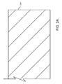
Fig. 2A illustrates an initial layer of magnetic material for use in forming a main pole, in accordance with one embodiment. -
Fig. 2B illustrates a beveled edge formed on the initial layer of magnetic material, in accordance with one embodiment. -
Fig. 2C illustrates an initial layer of material for use in the gap between two magnetic layers of material, in accordance with one embodiment. -
Fig. 2D illustrates a second layer of material for use in the gap between two magnetic layers of material, in accordance with one embodiment. -
Fig. 2E illustrates a sacrificial layer of material disposed over the initial gap materials, in accordance with one embodiment. -
Fig. 2F illustrates the sacrificial layer after processing has occurred that created an uneven surface to the sacrificial layer, in accordance with one embodiment. -
Fig. 2G illustrates further deposition of sacrificial layer material to form an even top surface to the sacrificial layer, in accordance with one embodiment. -
Fig. 2H illustrates a second magnetic material layer disposed above the sacrificial layer, in accordance with one embodiment. -
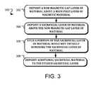
Fig. 3 shows a flow chart illustrating a method of forming a substantially uniform gap layer, in accordance with one embodiment. -
Fig. 4 shows a flow chart illustrating another embodiment of forming a gap layer, in accordance with one embodiment. -
Fig. 5 shows a flow chart illustrating a method of utilizing a non-magnetic seed layer in accordance with one embodiment. -
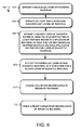
Fig. 6 shows a flow chart illustrating another embodiment of utilizing a non-magnetic seed layer in accordance with one embodiment. -
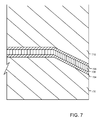
Fig. 7 shows a cross-section of a write gap for a write head having at least two layers of non-magnetic material in the write gap, in accordance with one embodiment. - Embodiments of the present technology are disclosed herein in the context of a disc drive system. However, it should be understood that the technology is not limited to a disc drive system and could readily be applied to other technology systems as well.
- As areal density of magnetic recording media increases, more and more bits of information are being stored on the magnetic media. Thus, there is a need to store each bit of information in a smaller storage location than has previously been used. As a result, the write head of a disc drive needs to be able to record the bit on the magnetic media without disrupting the information stored in neighboring bit locations.
- Write heads can be inefficient if there is a lack of a uniform gap between the magnetic material of the write pole and the magnetic material of the front shield. This non-uniformity allows more magnetic flux to leak from the write pole to the front shield during a write operation -- rather than being directed through the targeted bit location. As a result, the write pole is less efficient in its write operation when this leakage occurs. A more uniform gap or even a gap that diverges rather than converges (when viewed from the perspective of moving towards an air bearing surface) would cause less leakage to occur.
- In accordance with one embodiment a new process is disclosed that allows one to form a substantially uniform write gap between two magnetic materials as well as a resulting writer structure for a recording head. A magnetic overlayer with appropriate seeds (magnetic or non-magnetic) may also be formed on top of a non-magnetic write gap immediately following the deposition of any write gap layers of material. The write gap, together with the magnetic overlayer may be tailored to form a unique structure. In accordance with one embodiment, the process may be used to form a substantially uniform write gap, to reduce the gap thickness sigma, and to improve write performance of a write head with a narrow write gap. A deliberately selected non-magnetic seed may be used to enable a high moment magnetic layer to be in direct contact with a write gap without sacrificing the magnetic softness of the high moment magnetic materials. Moreover, configuring the material on both sides of the gap to have high moments without changing the magnetic softnesss of the magnetic materials can help to achieve improved writability. While the embodiments described as examples herein use a write head as an example, the process and structures may also be applied to other magnetic layers that are separated by a gap of material.
- With reference now to
FIG. 1 , an example of a disc drive system is shown. A disc drive system is but one example where disclosed technology may be utilized.FIG. 1 illustrates aperspective view 100 of an example. Adisc 102 rotates about a spindle center or a disc axis ofrotation 104 during operation. Thedisc 102 includes aninner diameter 106 and anouter diameter 108 between which are a number of concentric data tracks 110, illustrated by circular lines. The data tracks 110 are substantially circular. - Information may be written to and read from the bits on the
disc 102 in different data tracks 110. Atransducer head 124 is mounted on anactuator assembly 120 at an end distal to an actuator axis ofrotation 122. Thetransducer head 124 flies in close proximity above the surface of thedisc 102 during disc operation. Theactuator assembly 120 rotates during a seek operation about the actuator axis ofrotation 122 positioned adjacent to thedisc 102. The seek operation positions thetransducer head 124 over a target data track of the data tracks 110. - The exploded
view 140 illustrates a cross-section of a portion of the transducer head 124 (not to scale). The cross-section shows a substantially uniform write-gap that can be configured in accordance with one embodiment. - As the areal density of magnetic recording media increases, information can be stored in smaller and smaller locations. This requires that the read head and write heads be able to read from and write to, respectively, those locations. A write gap is the non-magnetic gap separating the main writer pole from the front shield in a write head. The thickness of the write gap and the magnetic materials that are in the vicinity of the write gap can have great impact upon the writability and the trailing edge (TE) field gradient. To date, the write gap thicknesses are in the range of about 30 nm.
- During the process of forming write gaps, it is not uncommon to perform photolithography and etch processes on the deposited write gap material. This results in the write gap being deteriorated unevenly across its surface. Where the write gap contains a bevel edge, one result is that the write gap can become tapered or pinched near the top of the bevel point. Thus, a non-uniform write gap is often produced by these photolithography and etching steps. A non-uniform write gap can result in more flux shunt to the front shield from the main writer pole during operation. This loss of flux makes a write operation less efficient and possibly defective. It can be referred to as suppressing writability.
- Referring now to
Figs. 2A ,2B ,2C ,2D ,2E ,2F ,2G , and2H a process for forming a more uniform write gap can be illustrated in accordance with one embodiment. This process may also be used to reduce the write gap sigma. It will also be appreciated from the following description that this process enables an alternative seed, such as Ruthenium, to be used as a seed layer for the 2.4T FeCo layer of the front shield. Moreover, such a seed layer allows a FeCo magnetic layer to be in intimate contact with the write gap in order to provide an enhanced TE field gradient. - In
Fig. 2A a first layer ofmagnetic material 204 is deposited. The magnetic material may be formed, for example, from FeCo. This layer of magnetic material may ultimately serve as the main write pole during operation of a write head. To form the main write pole, one may bevel themagnetic material layer 204 to form abevel edge 208 and abevel point 212, as shown inFig. 2B . The bevel may be formed by milling the magnetic layer, for example. - In
Fig. 2C , a first layer ofgap material 216 is shown deposited on the top of themagnetic material layer 204. One type of material that may be utilized is Ruthenium. Ruthenium is a non-magnetic material that can perform well as a gap material. It can also serve as a seed layer for a second layer of gap material. - In
Fig. 2D , a second layer ofgap material 220 is shown as deposited on the top of the first layer of gap material. One material that can be useful as a gap material is Al2O3 also referred to as alumina. - In
Fig. 2E , a first layer of sacrificial material is shown as deposited on the top of the second layer of gap material. Oftentimes, one will choose to perform photolithography and etching steps before depositing the final layer of magnetic material. Such processing steps can affect the uniformity of the gap materials that have previously been deposited -- particularly in the bevel edge region. One non-uniformity that can take place is that the write gap becomes tapered at the bevel point. As noted earlier, this can result in a non-uniform write-gap in a finished write head that causes decreased performance by the write head. Examples of processing steps that are often performed include a photolithography step that is followed by an etching step. Other processing steps might alternatively be performed. Regardless, the result is that the write gap is left in a non-uniform state. By utilizing a sacrificial layer that can be refurbished by deposition of additional sacrificial material, the uniformity of the gap can be substantially restored following the damaging processing steps. Thus,Fig. 2F shows the effects of the damaging processing steps on thesacrificial layer 224. As can be seen, the damaging processing steps leave the sacrificial layer in an uneven state, while the underlying gap layers are undamaged. It should be noted that the sacrificial layer may be seeded by a seed layer. One choice of seed layer material is Ruthenium. Other non-magnetic seed material may be used rather than Ruthenium. - In
Fig. 2G , additional sacrificial material may be deposited so as to restore the sacrificial layer to a substantially uniform thickness. The restored sacrificial layer is referred to aslayer 226 inFig. 2G . The sacrificial layer can also be selected so as to serve as a seed layer for a subsequent magnetic layer. - Once the gap is restored to a substantially uniform thickness, a second layer of magnetic material may be deposited. For example,
Fig. 2H shows a second layer ofmagnetic material 228 that may be used as a front shield for a write head. One may utilize FeCo or FeNiCo solid solutions as the magnetic material, for example. The thickness may be in the range of a few nanometers to a few hundreds of nanometers. In accordance with one embodiment, a thickness of 5-50 nm may be used. - As can be seen from
Fig. 2H , the resulting write gap is substantially uniform and is not affected by the intermediate photolithography and etching steps that take place before the deposition of the second layer of magnetic material. - Referring now to
Fig. 3 , aflow chart 300 illustrating aspects of the above-described process can be seen. Inblock 302, a non-magnetic gap layer of material may be deposited above a main pole layer of magnetic material. Inblock 304, a sacrificial layer of material may be deposited above the non-magnetic gap layer of material. In block 306, a portion of the sacrificial layer may be processed, for example by an etch process, while not entirely removing the sacrificial layer of material. And, inblock 308, additional sacrificial material may be deposited to the etched sacrificial layer. - In
Fig 4 , aflow chart 400 illustrates a more detailed embodiment. Inblock 402, a non-magnetic layer of material is deposited above a main pole layer of magnetic material. The main pole layer of magnetic material may already be in a beveled configuration. It should be appreciated that multiple layers and different materials may be used to form the gap.Block 404 illustrates that a sacrificial layer of material may be deposited on top of the top non-magnetic gap layer of material. - According to block 406, an etch or other processing step may be performed on the structure. Such processing may remove portions of the sacrificial layer while not necessarily removing the entire sacrificial layer so as to expose any underlying layers, particularly along the bevel edge area. The result of the etching or other processing will be that the sacrificial layer will be uneven. Thus, in
block 408, additional sacrificial material may be deposited on the etched sacrificial layer. The deposition can be controlled so as to form a substantially uniform gap between the main pole layer and a subsequently applied front shield layer, as shown inblock 410. Then, a front shield layer of material may be applied on top of the sacrificial layer. - In accordance with another embodiment, a different utility can be achieved. Namely, current processes typically utilize a magnetic material such as NiFe as a seed layer prior to depositing a layer of magnetic material, such as FeCo, as the front shield layer. The NiFe has a magnetic moment property of about 1.0T. This use of magnetic material as the seed layer can degrade the trailing edge (TE) field gradient which in turn decreases the performance of the recording head.
- To address this issue, one embodiment utilizes a non-magnetic material as the seed layer for the magnetic material used in the front shield layer. This non-magnetic material allows a better field gradient to be achieved in contrast to a magnetic material such as NiFe. Different materials may be utilized as the non-magnetic material seed layer. But, one possible choice is Ruthenium. Other possible materials are NiRu, NiCr, Cu, and high moment material with combinations of Fe, Ni, and Co alloys, for example. The thickness of the seed layer can be in the range of 1-10 nm, for example.
- The deposition process can be similar to that shown with respect to
Figs. 2A through 2H where a non-magnetic seed layer is utilized for a second layer of magnetic material. Moreover,Fig. 5 illustrates a flow chart demonstrating various aspects. - In
flow chart 500 ofFig. 5 , block 502 shows that a main pole layer of magnetic material is deposited. Inblock 504, at least two non-magnetic gap layers of material are deposited. And, inblock 506, a second layer of magnetic material is deposited. Notably, the second layer of magnetic material is deposited directly adjacent to the upper layer of non-magnetic gap material. This allows the non-magnetic gap material to serve as a seed layer for the second layer of magnetic material. -
Fig. 6 illustrates a somewhat more detailed embodiment. Inflow chart 600 ofFig. 6 , a main pole layer of magnetic material is deposited, inblock 602. Inblock 604, at least two non-magnetic gap layers of material are deposited. As noted in an earlier embodiment, the gap may be formed from multiple layers, such as a first layer of Ruthenium followed by a layer of Al2O3, and followed by a seed layer of Ruthenium. - In
block 606, a second layer of magnetic material may be deposited. This layer may be used, for example, as a front shield in a write head. This second layer may be deposited directly adjacent the non-magnetic gap material so as to form a sufficient gradient. Moreover, this non-magnetic gap material may be used as a seed layer for the second layer of magnetic material, as shown byblock 608. As shown byblock 610, FeCo may be utilized as the material for the second layer of magnetic material.Block 612 illustrates that the second layer of magnetic material may be formed into a front shield for use in a write head. -
Fig. 7 illustrates an example of a gap layer that is formed from two or more gap layers of non-magnetic material.Fig. 7 shows a first layer ofmagnetic material 702 that serves as the write head. FeCo is one type of magnetic material that can be used for the first magnetic layer. A first gap layer ofnon-magnetic material 704 is shown disposed above and directly adjacent to the magnetic material. One material that can be used, for example, is Ruthenium. A second gap layer ofnon-magnetic material 706 is shown disposed above and directly adjacent the first gap layer. For example, Al2O3 is one type of material that could be used for this material. A third gap layer ofnon-magnetic material 708 is shown disposed above and directly adjacent the second gap layer. The material Ruthenium could be utilized for this layer to provide symmetry with the first gap layer. Moreover, Ruthenium is useful in serving as a seed layer for the second layer ofmagnetic material 710. Thelayer 710 is shown disposed above and directly adjacent to the third gap layer. FeCo is one example of a magnetic material that can be used forlayer 710 in order to serve as a front shield for the main pole. - It is noted that many of the structures, materials, and acts recited herein can be recited as means for performing a function or step for performing a function. Therefore, it should be understood that such language is entitled to cover all such structures, materials, or acts disclosed within this specification and any modifications falling within the scope of the claims.
- It is thought that the apparatuses and methods of embodiments described herein will be understood from this specification. While the above description is a complete description of specific embodiments, the above description should not be taken as limiting the scope of the patent as defined by the claims.
Claims (20)
- A method of forming a uniform gap between two magnetic materials, the method comprising:depositing a non-magnetic gap layer (216, 220) of material above a main pole layer (204) of magnetic material;
depositing a sacrificial (224) layer of material above the non-magnetic gap layer of material;
etching a portion of the sacrificial layer of material while not entirely removing the sacrificial layer of material;
depositing additional sacrificial material (226) to the etched sacrificial layer. - The method as claimed in claim 1 and further comprising:depositing a front shield layer (228) on top of the sacrificial layer.
- The method as claimed in claim 2 and further comprising:forming a substantially uniform gap between the main pole layer (204) and the front shield layer (228).
- The method as claimed in any one of the preceding claims wherein the non-magnetic gap layer (220) comprises Al2O3.
- The method as claimed in any one of claims 1 to 3 wherein the non-magnetic gap layer (216) comprises Ruthenium.
- The method as claimed in any one of the preceding claims wherein the sacrificial layer (224) comprises Ruthenium.
- The method as claimed in any one of the preceding claims wherein the sacrificial layer comprises NiRu.
- The method as claimed in any one of claims 1 to 5 wherein the sacrificial layer comprises Cu.
- The method as claimed in any one of the preceding claims wherein the sacrificial layer material comprises a magnetic moment of about the same magnetic moment of the main pole material.
- The method as claimed in any one of the preceding claims wherein the sacrificial layer material utilizes a non-magnetic seed material.
- An apparatus comprising:a main pole layer (204) of magnetic material;a non-magnetic gap layer (216, 220) of material above the main pole layer;an etched first sacrificial layer (224) of material above the non-magnetic gap layer of material; anda second sacrificial layer (226) of material above the etched first sacrificial layer of material.
- The apparatus as claimed in claim 11 and further comprising:a front shield layer (228) on top of the sacrificial layer.
- The apparatus as claimed in claim 12 and further comprising:a substantially uniform gap between the main pole layer (204) and the front shield layer (228).
- The apparatus as claimed in any one of claims 11 to 13 wherein the non-magnetic layer (220) comprises Al2O3.
- The apparatus as claimed in any one of claims 11 to 13 wherein the non-magnetic layer comprises Ruthenium.
- The apparatus as claimed in any one of claims 11 to 15 wherein the first sacrificial layer (224) comprises Ruthenium.
- The apparatus as claimed in any one of claims 11 to 16 wherein the first sacrificial layer (224) comprises NiRu.
- The apparatus as claimed in any one of claims 11 to 15 wherein the first sacrificial layer comprises Cu.
- The apparatus as claimed in any one of claims 11 to 18 wherein the first sacrificial layer material comprises a magnetic moment approximately equivalent to the magnetic moment of the main pole material.
- The apparatus as claimed in any one of claims 11 to 19 wherein the first sacrificial layer material utilizes a non-magnetic seed material.
Applications Claiming Priority (1)
| Application Number | Priority Date | Filing Date | Title |
|---|---|---|---|
| US13/796,951 US9214167B2 (en) | 2013-03-12 | 2013-03-12 | Main pole layer with at least tow sacrificial layers and a gap layer |
Publications (2)
| Publication Number | Publication Date |
|---|---|
| EP2779165A2 true EP2779165A2 (en) | 2014-09-17 |
| EP2779165A3 EP2779165A3 (en) | 2015-03-25 |
Family
ID=50276974
Family Applications (1)
| Application Number | Title | Priority Date | Filing Date |
|---|---|---|---|
| EP14159148.7A Withdrawn EP2779165A3 (en) | 2013-03-12 | 2014-03-12 | Gap between magnetic materials |
Country Status (5)
| Country | Link |
|---|---|
| US (2) | US9214167B2 (en) |
| EP (1) | EP2779165A3 (en) |
| JP (1) | JP6066947B2 (en) |
| KR (1) | KR101763198B1 (en) |
| CN (1) | CN104050986B (en) |
Families Citing this family (2)
| Publication number | Priority date | Publication date | Assignee | Title |
|---|---|---|---|---|
| US9214167B2 (en) | 2013-03-12 | 2015-12-15 | Seagate Technology Llc | Main pole layer with at least tow sacrificial layers and a gap layer |
| US9147407B2 (en) | 2013-03-12 | 2015-09-29 | Seagate Technology Llc | Write head having non-magnetic write gap seed layer, and method |
Family Cites Families (54)
| Publication number | Priority date | Publication date | Assignee | Title |
|---|---|---|---|---|
| US3959824A (en) | 1970-11-30 | 1976-05-25 | Tohoku Metal Industries Limited | Two gap read/write head assembly |
| US4992901A (en) * | 1990-02-15 | 1991-02-12 | Seagate Technology, Inc. | Self aligned magnetic poles using sacrificial mask |
| JP2990885B2 (en) * | 1991-09-12 | 1999-12-13 | 株式会社日立製作所 | Thin-film magnetic head and magnetic disk drive using the same |
| US5729413A (en) | 1995-12-20 | 1998-03-17 | Ampex Corporation | Two-gap magnetic read/write head |
| JP3305244B2 (en) | 1997-12-10 | 2002-07-22 | アルプス電気株式会社 | Thin film magnetic head and method of manufacturing the same |
| JPH11195206A (en) * | 1997-12-26 | 1999-07-21 | Hitachi Metals Ltd | Magnetoresistive thin film magnetic head and production thereof |
| US6724569B1 (en) | 2000-02-16 | 2004-04-20 | Western Digital (Fremont), Inc. | Thin film writer with multiplayer write gap |
| JP2003006813A (en) | 2001-06-20 | 2003-01-10 | Shinka Jitsugyo Kk | Thin film magnetic head and its manufacturing method |
| US6876507B2 (en) | 2002-01-18 | 2005-04-05 | International Business Machines Corporation | High-saturation thin-film write head for high-coercivity magnetic data storage media |
| US6975486B2 (en) | 2002-08-06 | 2005-12-13 | Western Digital (Fremont), Inc. | Thin film write head having a laminated, flat top pole with bottom shaper and method of fabrication |
| US7587810B2 (en) | 2004-04-30 | 2009-09-15 | Hitachi Global Storage Technologies Netherlands B.V. | High milling resistance write pole fabrication method for perpendicular recording |
| US7649712B2 (en) | 2004-08-31 | 2010-01-19 | Hitachi Global Storage Technologies Netherlands B.V. | Self aligned wrap around shield for perpendicular magnetic recording |
| US7633713B2 (en) | 2005-01-31 | 2009-12-15 | Hitachi Global Storage Technologies Netherlands B.V. | Method for controlling the formation of the trailing shield gap during perpendicular head fabrication and head formed thereby |
| US7525760B2 (en) | 2005-04-11 | 2009-04-28 | Hitachi Global Storage Technologies B.V. | Laminated write gap to improve writer performance |
| JP2007087551A (en) * | 2005-09-26 | 2007-04-05 | Alps Electric Co Ltd | Manufacturing method of perpendicular magnetic recording head |
| US7791844B2 (en) * | 2005-12-14 | 2010-09-07 | Hitachi Global Storage Technologies Netherlands B.V. | Magnetoresistive sensor having a magnetically stable free layer with a positive magnetostriction |
| US7898773B2 (en) | 2006-02-02 | 2011-03-01 | Headway Technologies, Inc. | Perpendicular magnetic recording head with a side write shield |
| US7631417B2 (en) | 2006-11-10 | 2009-12-15 | Hitachi Global Storage Technologies Netherlands B.V. | Use of anti-reflective seed layers for the fabrication of perpendicular thin film heads |
| US8238056B2 (en) | 2007-11-02 | 2012-08-07 | Headway Technologies, Inc. | Perpendicular shield pole writer with tapered main pole and tapered non-magnetic top shaping layer |
| US8018679B2 (en) | 2007-12-17 | 2011-09-13 | Hitachi Global Storage Technologies Netherlands B.V. | Perpendicular magnetic recording write head with slanted magnetic write pole |
| US8143092B2 (en) * | 2008-03-10 | 2012-03-27 | Pragati Kumar | Methods for forming resistive switching memory elements by heating deposited layers |
| US8146236B1 (en) | 2008-03-28 | 2012-04-03 | Western Digital (Fremont), Llc | Method for providing a perpendicular magnetic recording (PMR) transducer |
| US8031433B2 (en) | 2008-09-05 | 2011-10-04 | Headway Technologies, Inc. | Method to make an integrated side shield PMR head with non conformal side gap |
| US8724258B2 (en) * | 2009-09-30 | 2014-05-13 | HGST Netherlands B.V. | Slanted bump design for magnetic shields in perpendicular write heads and method of making same |
| US8451560B2 (en) | 2009-12-09 | 2013-05-28 | HGST Netherlands B.V. | Magnetic head with flared write pole with multiple non-magnetic layers thereover |
| US8441757B2 (en) * | 2009-12-09 | 2013-05-14 | HGST Netherlands B.V. | Perpendicular magnetic write head with wrap-around shield, slanted pole and slanted pole bump fabricated by damascene process |
| US8323727B2 (en) * | 2009-12-17 | 2012-12-04 | Hitachi Global Storage Technologies Netherlands B.V. | Method for manufacturing a perpendicular magnetic write head having a tapered write pole and a stepped wrap around side shield gap |
| US8341826B1 (en) | 2010-04-12 | 2013-01-01 | Western Digital (Fremont), Llc | Method for fabricating a magnetic recording transducer using a split seed layer |
| US8611046B2 (en) | 2010-04-19 | 2013-12-17 | Headway Technologies, Inc. | PMR writer with graded side shield |
| US8409453B1 (en) | 2010-05-12 | 2013-04-02 | Western Digital (Fremont), Llc | Method and system for providing a wrap-around shield using a patterned seed layer |
| US8454846B1 (en) | 2010-06-17 | 2013-06-04 | Western Digital (Fremont), Llc | Method and system for providing a full wrap-around shield using a frame configured wet etch in a damascene process |
| DE102010031087A1 (en) | 2010-07-08 | 2012-01-12 | Evonik Goldschmidt Gmbh | Novel polyester-modified organopolysiloxanes |
| CN102437032B (en) * | 2010-09-29 | 2015-04-01 | 中国科学院微电子研究所 | Fabrication method of metal grid in gate-last process |
| US8254059B2 (en) | 2010-12-06 | 2012-08-28 | Hitachi Global Storage Technologies Netherlands B.V. | Perpendicular magnetic recording head with domain controlled side shield |
| US20120154951A1 (en) * | 2010-12-21 | 2012-06-21 | Hitachi Global Storage Technologies Netherlands B.V. | Method for manufacturing a perpendicular magnetic write pole having a write pole and trailing shield with a tapered trailing gap |
| US20120164486A1 (en) | 2010-12-22 | 2012-06-28 | Bonhote Christian Rene | Nicr as a seed stack for film growth of a gap layer separating a magnetic main pole or shield |
| US8238059B1 (en) * | 2011-04-06 | 2012-08-07 | Headway Technologies, Inc. | PMR write head with narrow gap for minimal internal flux loss |
| US8564903B2 (en) * | 2011-05-16 | 2013-10-22 | Headway Technologies, Inc. | Writer with an AFM write gap |
| US8578594B2 (en) | 2011-06-06 | 2013-11-12 | Western Digital (Fremont), Llc | Process for fabricating a magnetic pole and shields |
| US20130020204A1 (en) | 2011-07-20 | 2013-01-24 | Hitachi Global Storage Technologies Netherlands B. V. | Magnetic write head having an electroplated write pole with a leading edge taper |
| US8451563B1 (en) * | 2011-12-20 | 2013-05-28 | Western Digital (Fremont), Llc | Method for providing a side shield for a magnetic recording transducer using an air bridge |
| US8259540B1 (en) | 2012-01-16 | 2012-09-04 | Seagate Technology Llc | Heat assisted magnetic recording (HAMR) heads including components made of nickel alloys |
| US8570686B2 (en) * | 2012-03-13 | 2013-10-29 | HGST Netherlands B.V. | Magnetic recording head with non-conformal side shield gap |
| US8416528B1 (en) | 2012-05-03 | 2013-04-09 | Headway Technologies, Inc. | Magnetic head for perpendicular magnetic recording having a return path section |
| US8724259B1 (en) | 2012-06-11 | 2014-05-13 | Western Digital (Fremont), Llc | Conformal high moment side shield seed layer for perpendicular magnetic recording writer |
| US8498079B1 (en) | 2012-09-15 | 2013-07-30 | Headway Technologies, Inc. | Superior performance head design with minimized ATE and WATE |
| US8482879B1 (en) | 2012-12-13 | 2013-07-09 | Headway Technologies, Inc. | Magnetic head for perpendicular magnetic recording having a return path section |
| US8842390B2 (en) | 2013-01-18 | 2014-09-23 | Seagate Technology Llc | Write pole box shield |
| US9214167B2 (en) | 2013-03-12 | 2015-12-15 | Seagate Technology Llc | Main pole layer with at least tow sacrificial layers and a gap layer |
| US9147407B2 (en) * | 2013-03-12 | 2015-09-29 | Seagate Technology Llc | Write head having non-magnetic write gap seed layer, and method |
| US8767347B1 (en) | 2013-05-28 | 2014-07-01 | Headway Technologies, Inc. | Magnetic head for perpendicular magnetic recording having two side shields |
| US9318131B2 (en) * | 2013-06-28 | 2016-04-19 | Seagate Technology Llc | Write gap structure for a magnetic recording head |
| US9305583B1 (en) | 2014-02-18 | 2016-04-05 | Western Digital (Fremont), Llc | Method for fabricating a magnetic writer using multiple etches of damascene materials |
| US9299367B1 (en) | 2015-07-30 | 2016-03-29 | Headway Technologies, Inc. | Perpendicular magnetic recording (PMR) writer with minimized internal flux shunting |
-
2013
- 2013-03-12 US US13/796,951 patent/US9214167B2/en not_active Expired - Fee Related
-
2014
- 2014-03-06 KR KR1020140026632A patent/KR101763198B1/en not_active Expired - Fee Related
- 2014-03-11 JP JP2014047620A patent/JP6066947B2/en not_active Expired - Fee Related
- 2014-03-11 CN CN201410086587.2A patent/CN104050986B/en not_active Expired - Fee Related
- 2014-03-12 EP EP14159148.7A patent/EP2779165A3/en not_active Withdrawn
-
2015
- 2015-11-23 US US14/949,638 patent/US9922671B2/en not_active Expired - Fee Related
Non-Patent Citations (1)
| Title |
|---|
| None |
Also Published As
| Publication number | Publication date |
|---|---|
| JP2014175048A (en) | 2014-09-22 |
| KR101763198B1 (en) | 2017-07-31 |
| US20160078887A1 (en) | 2016-03-17 |
| US9214167B2 (en) | 2015-12-15 |
| KR20140111962A (en) | 2014-09-22 |
| US20140268415A1 (en) | 2014-09-18 |
| US9922671B2 (en) | 2018-03-20 |
| CN104050986A (en) | 2014-09-17 |
| JP6066947B2 (en) | 2017-01-25 |
| EP2779165A3 (en) | 2015-03-25 |
| CN104050986B (en) | 2018-06-19 |
Similar Documents
| Publication | Publication Date | Title |
|---|---|---|
| US9761252B2 (en) | Write head having beveled non-magnetic write gap seed layer | |
| JP2012003834A (en) | Manufacturing method of thin film magnetic head, and thin film magnetic head | |
| US20140177102A1 (en) | Multi-reader method and apparatus | |
| US8508886B2 (en) | Use of magnetic material for RIE stop layer during damascene main pole formation | |
| US9922671B2 (en) | Main pole layer with at least two sacrificial layers and a gap layer | |
| US7648731B2 (en) | Fabricating perpendicular write elements in perpendicular magnetic recording heads | |
| US20100155364A1 (en) | Magnetic write head having a stepped trailing shield and write pole with a sloped trailing edge | |
| JP5720871B2 (en) | Method for forming a conversion head having a magnetic recording element | |
| US10339964B1 (en) | Perpendicular magnetic recording (PMR) write head with patterned high moment trailing shield | |
| US20090273862A1 (en) | Flat e-yoke for cusp write head | |
| US8619391B2 (en) | Magnetic write heads with bi-layer wrap around shields having dissimilar shield layer widths | |
| US9384769B2 (en) | Write pole configuration | |
| US20170092306A1 (en) | Magnetic recording head front shield formation | |
| US9406323B2 (en) | Slider with aluminum compound fill | |
| US7243411B2 (en) | Method for protecting write head coil during write pole/shaping | |
| US8449752B2 (en) | Trailing plated step | |
| US9082427B1 (en) | Write head having reduced dimensions | |
| US7768748B2 (en) | Magnetoresistive sensor with overlaid combined leads and shields |
Legal Events
| Date | Code | Title | Description |
|---|---|---|---|
| 17P | Request for examination filed |
Effective date: 20140331 |
|
| AK | Designated contracting states |
Kind code of ref document: A2 Designated state(s): AL AT BE BG CH CY CZ DE DK EE ES FI FR GB GR HR HU IE IS IT LI LT LU LV MC MK MT NL NO PL PT RO RS SE SI SK SM TR |
|
| AX | Request for extension of the european patent |
Extension state: BA ME |
|
| PUAI | Public reference made under article 153(3) epc to a published international application that has entered the european phase |
Free format text: ORIGINAL CODE: 0009012 |
|
| RIN1 | Information on inventor provided before grant (corrected) |
Inventor name: YIN, HUAQING Inventor name: LIN, DOUG Inventor name: QIU, JIAOMING Inventor name: INTURI, VENKATESWARA RAO Inventor name: TIAN, WEI |
|
| PUAL | Search report despatched |
Free format text: ORIGINAL CODE: 0009013 |
|
| AK | Designated contracting states |
Kind code of ref document: A3 Designated state(s): AL AT BE BG CH CY CZ DE DK EE ES FI FR GB GR HR HU IE IS IT LI LT LU LV MC MK MT NL NO PL PT RO RS SE SI SK SM TR |
|
| AX | Request for extension of the european patent |
Extension state: BA ME |
|
| RIC1 | Information provided on ipc code assigned before grant |
Ipc: G11B 5/235 20060101ALI20150217BHEP Ipc: G11B 5/23 20060101ALI20150217BHEP Ipc: G11B 5/31 20060101AFI20150217BHEP |
|
| RBV | Designated contracting states (corrected) |
Designated state(s): AL AT BE BG CH CY CZ DE DK EE ES FI FR GB GR HR HU IE IS IT LI LT LU LV MC MK MT NL NO PL PT RO RS SE SI SK SM TR |
|
| 17Q | First examination report despatched |
Effective date: 20160318 |
|
| STAA | Information on the status of an ep patent application or granted ep patent |
Free format text: STATUS: THE APPLICATION IS DEEMED TO BE WITHDRAWN |
|
| 18D | Application deemed to be withdrawn |
Effective date: 20160929 |