EP2778946A2 - Hybrid programmable many-core device with on-chip interconnect - Google Patents
Hybrid programmable many-core device with on-chip interconnect Download PDFInfo
- Publication number
- EP2778946A2 EP2778946A2 EP14158110.8A EP14158110A EP2778946A2 EP 2778946 A2 EP2778946 A2 EP 2778946A2 EP 14158110 A EP14158110 A EP 14158110A EP 2778946 A2 EP2778946 A2 EP 2778946A2
- Authority
- EP
- European Patent Office
- Prior art keywords
- processors
- programmable logic
- logic elements
- data
- hybrid
- Prior art date
- Legal status (The legal status is an assumption and is not a legal conclusion. Google has not performed a legal analysis and makes no representation as to the accuracy of the status listed.)
- Ceased
Links
Images




Classifications
-
- G—PHYSICS
- G06—COMPUTING OR CALCULATING; COUNTING
- G06F—ELECTRIC DIGITAL DATA PROCESSING
- G06F15/00—Digital computers in general; Data processing equipment in general
- G06F15/76—Architectures of general purpose stored program computers
-
- G—PHYSICS
- G06—COMPUTING OR CALCULATING; COUNTING
- G06F—ELECTRIC DIGITAL DATA PROCESSING
- G06F15/00—Digital computers in general; Data processing equipment in general
- G06F15/76—Architectures of general purpose stored program computers
- G06F15/78—Architectures of general purpose stored program computers comprising a single central processing unit
- G06F15/7867—Architectures of general purpose stored program computers comprising a single central processing unit with reconfigurable architecture
-
- Y—GENERAL TAGGING OF NEW TECHNOLOGICAL DEVELOPMENTS; GENERAL TAGGING OF CROSS-SECTIONAL TECHNOLOGIES SPANNING OVER SEVERAL SECTIONS OF THE IPC; TECHNICAL SUBJECTS COVERED BY FORMER USPC CROSS-REFERENCE ART COLLECTIONS [XRACs] AND DIGESTS
- Y02—TECHNOLOGIES OR APPLICATIONS FOR MITIGATION OR ADAPTATION AGAINST CLIMATE CHANGE
- Y02D—CLIMATE CHANGE MITIGATION TECHNOLOGIES IN INFORMATION AND COMMUNICATION TECHNOLOGIES [ICT], I.E. INFORMATION AND COMMUNICATION TECHNOLOGIES AIMING AT THE REDUCTION OF THEIR OWN ENERGY USE
- Y02D10/00—Energy efficient computing, e.g. low power processors, power management or thermal management
Definitions
- the term "tiled” refers to arranging the processors such that they are interleaved or interspersed among programmable logic elements.
- the processors may be arranged consecutively in a two dimensional plane with the programmable logic elements such that there are no other programmable logic elements between consecutive processors. This tiling of the processors may allow for efficient fabrication and provisioning of interconnect networks for communicating between the processors, programmable logic elements, and I/O interfaces of the device.
- the hybrid programmable logic device may include scheduling circuitry that can schedule the transmission of data on the horizontal and vertical connectors in the logic fabric that transmit data between the programmable logic elements and processors.
- this scheduling circuitry may receive interrupt messages addressed to at least one of the processors, meaning that they contain information that indicate that the payload of the data is meant to be processed by a particular processor or processors.
- the scheduling circuitry may use other methods of asynchronous communication to send data between the programmable logic elements and the processors.
- the scheduling circuitry may identify which of the processors are meant to process a particular data (e.g., a block or packet of data), and distribute the data to the identified processors.
- the scheduling circuitry may allow the processors, the programmable logic elements, and the data bus to run at different clock speeds, thus breaking any timing dependency between the network bus and the processor clock speed.
- processors and programmable logic may be divided into partitions in order to manage power. For example, partitions of the hybrid programmable logic device may be computed. Each partition may include a subset of the processors and programmable logic elements. At least one measure of processor demand may be computed, and based on this measure the power state of the processors and programmable logic elements in a partition may be altered. This feature may allow the power consumption of the device to be dynamically managed based on the throughput to particular groups of processors and programmable logic elements.
- many agents may request intermittent access to external memory. For example, when the many-core device receives a packet, the payload is split from the header and sent to external memory (or internal buffer) while the header is sent to a processing unit (e.g., a microprocessor or hardware block) for a large amount of processing time (e.g., hundreds of clock cycles). The resulting header, which is possibly modified, is then rejoined with its payload and queued for forwarding off-device. When hundreds of agents are sending and receiving data, coordinating access to memory may be difficult. It would therefore be desirable to design a many-core device with a shared interconnect that allows for flexible routing (e.g., dynamic routing as compared to static routing).
- a processing unit e.g., a microprocessor or hardware block
- FIG. 1A is a hybrid programmable logic device 100 in accordance with an embodiment of the present invention.
- Device 100 includes regions of programmable logic elements 130, and processors 150.
- General purpose input / output circuitry 110 can include one or more generic pins that can be controlled or programmed by external software at runtime.
- general purpose input / output circuitry 110 can be configured to input or output data, can read or write data, can be used as IRQs for wakeup events, or can be used to transfer data from sources peripheral to device 100.
- High-speed serial interface 120 can facilitate the transfer of information between external sources of data (not shown), programmable logic elements 130, and processors 150 using high-speed transceiver blocks.
- Processors 150 can include any suitable number of processors with many-core designs. These many-core designs may be based on microprocessor IP by vendors such as ARM, MIPS, and Tensilica. This microprocessor IP allows for the ability to create customized embedded processors (e.g., removing floating-point units), and customized instruction set architectures. In certain embodiments, the processors may be "hardened,” meaning that they consist of fixed logic elements rather than programmable logic elements. This feature provides the integration of powerful many-core processors into a programmable logic fabric.
- processors 150 are tiled in a four-column assembly structure in portions of the device 100 where programmable logic elements 130 are not present. In other embodiments, fewer or greater columns of processors may be used. In certain embodiments, the number of columns or processors, and the number of processors in each column may be more or less than depicted in FIG. 1A . The number of columns and number of processors 150 in each column may depend on the processor architecture for each processor. For example, more processors may be tiled on device 100 when the instruction cache and data cache of each processor is reduced. In one example, MIPS 34K multi-threaded processors with 16KB of instruction cache and data cache are used.
- processors 150 are multi-threaded.
- Multi-threaded processors provide advantages to applications where it is commonly required to interface with an off-chip memory or lookup which could take multiple clock cycles of processing time, and thus increase latency, or to hide the latency of accelerator processing. For example, by blocking one thread in a processor to this lookup task, the processor is able to proceed with performing other functions.
- the multi-threading may be achieved by time-slicing operation on data received by the processors 150. In other embodiments, the multi-threading may be achieved by well-known operating system mechanisms.
- the tiled layout of processors 150 on the device allows for efficient fabrication and provisioning of interconnect networks for communicating between the processors, programmable logic elements, and I/O interfaces of the device. This is because the programmable logic elements 130 and other elements of device 100 such as memory (not shown) are separate from processors 150.
- the tiled layout of processors 150 allows for the construction of processors 150 and programmable logic elements 130 in the same metal layers in device 100, as well the construction of an interconnect stack containing a data bus.
- FIG. 1B is an expanded view of the hybrid programmable logic device 100 containing processors 150 adjacent to programmable logic elements 130 in accordance with an embodiment of the present invention.
- Two processors are depicted schematically in FIG. 1B as squares containing three components - processor core 170, instruction cache 180, and data cache 190.
- programmable logic elements 130 that are grouped into LABs 132.
- the physical size of a dimension of the processors 150 such as length, height, or width, is a multiple of the same dimension of the programmable logic elements 150, or LABs made up of programmable logic elements 150.
- the width of each of the two processors is equal to three LABs 132. This allows for efficient assembly of devices having different dimensions, with differing ratios of processors to programmable logic elements or other logic blocks.
- horizontal and vertical connectors 167 may also be included on device 100. As will be discussed below with respect to FIG. 3 , horizontal and vertical connectors 167 may transfer data between processors 150, programmable logic elements 120, general input / output interfaces, and memory on and off chip. In certain embodiments, horizontal and vertical connectors may be wired to interface circuitry 161 such that any signal from any of the programmable logic elements 130 can be delivered to interface port 166 via LIM / LEIM circuitry 162 and interface logic 164. For example, multiplexors within the LIM / LEIM circuitry 162 may choose which signal drives any global wire in the horizontal / vertical connectors 167 to connect any of the programmable logic elements 130 with processors 150.
- both the wiring from processor 217 and LABs 215 and LAB 216 are in the same metal layer in the interconnect stack (e.g., in a metal layer above the metal layers containing the LABs and processors).
- Hardened data bus 160 may consist of dedicated circuit components that transfer data to and from processors 150, programmable logic elements 130, ingress / egress processing block 136, external memory 135, and embedded ternary-CAM memory 137, rather than being reserved for other uses on the device.
- hardened data bus 160 may be referred to as a network on chip interconnect.
- hardened data bus 160 may be dedicated to routing and / or carrying the data to and from the ingress / egress processing block to other elements of the device. Hardened data bus 160 can allow for high performance data transfer both internal and external to the device.
- hardened data bus 160 may include a portion of horizontal and vertical connectors 167 ( FIG. 1C ) and data bus 210 ( FIGs. 2A and 2B ). In other embodiments, hardened data bus 160 may be entirely separate from horizontal and vertical connectors 167.
- portions of hardened data bus 160 may be connected or disconnected hierarchically by software that can program device 300.
- This software may include Quartus software design by Altera Corporation of San Jose, California, or any other suitable software.
- the bandwidth of hardened data bus 160 is designed to achieve the line-rate of a particular application. For example, if hardened data bus 160 is 64 bits and operating at 1 GHz with 80% efficiency, it can provide 51Gbps of bandwidth and be used to target a 50Gbps streaming video application. In another example, if hardened data bus 160 is 64 bits and operating at 1.5 GHz with 80% efficiency, it can provide 150Gbps of bandwidth and target an 100Gb traffic switch application.
- separate hardened data buses may be added to carry data for processor input and output, as LAB input and output.
- External memory 135 may include any suitable interface to external memory, such as DDR memory. External memory 135 can buffer data in applications where device 300 is processing video data or packet data.
- embedded ternary-CAM memory 137 may include any suitable block of content addressable memory, which is useful for networking applications.
- embedded ternary-CAM memory 137 may interface with programmable logic elements 130 and processors 150 using circuitry substantially similar to interface circuitry 161 ( FIG. 1C ).
- ternary-CAM memory 137 may be replaced by an SRAM or embedded SRAM packet buffer memory.
- Scheduling circuitry 600 includes bus interface 610 and threading circuitry 620.
- scheduling circuitry may also include processor 630 and cache 640.
- Processor 630 may be substantially similar to processors 150 ( FIG. 1A ), and cache 640 may be substantially similar to instruction cache 180 and data cache 190.
- processor 630 may be part of a tiled column or row of processors, such as that discussed with respect to processors 150 ( FIG. 1A ).
- scheduling circuitry 600 may be implemented on the device for every processor in the tiled rows or columns of processors.
- bus interface 610 may provide mechanisms that allow data to be transmitted on the horizontal and vertical connectors 605 at a rate asynchronous with respect to the speed of the clock of processor 630.
- bus interface 610 may receive interrupt messages over horizontal and vertical connectors 605.
- these interrupt messages may be addressed to one or more of the processors on the device, meaning that they contain information that indicate that the payload of the data associated with the messages is meant to be processed by a particular processor or processors.
- Bus interface circuitry 610 may transmit only the data associated with interrupt messages that are addressed to processor 630, and ignore other messages that are not addressed to processor 630.
- bus interface circuitry 610 may contain a predetermined or hardcoded value, either in software or hardware associated with bus circuitry 610, that is the address of processor 630. Bus interface circuitry 610 may periodically or constantly monitor the messages transmitted over horizontal and vertical connectors 605 for the address. When the address is detected, bus interface circuitry 610 may buffer data associated with the message addressed to processor 630, and transmit the data from the buffer to processor 630 using threading circuitry 620. Threading circuitry 620 maintains one or more program counters associated with the execution of various tasks in processor 630. In certain embodiments, threading circuitry 620 receives data from bus interface circuitry 610, and determines the appropriate time to send that data to processor 630 based on one or more of the program counters that it maintains. In this manner, scheduling circuitry 600 may allow the processors, programmable logic elements, and the data bus of a device to operate at different clock speeds, thus breaking any timing or clock dependency between the components tied to the network bus and the processor clock speed.
- scheduling circuitry 600 may include a program instruction memory (not shown), which can include any suitable combination of external memory.
- the instruction set of the processors on the device such as processor 630, may be modified during operation such that they are reprogrammed with a new instruction set. This new instruction set may allow the device to achieve new or different functionality, such as program instructions for a hardware accelerator that may be used by the processors.
- processors and programmable logic elements may be used to manage power usage of device 100.
- processors and programmable logic elements associated with partitions of device 100 may be powered up and down dynamically based on the demand for the processing capabilities of the processors and logic elements associated with each partition. This process is described with respect to FIG. 7B below.
- the scheduling software may change the partitions dynamically during the operation of the device. For example, at a first time the scheduling software may designate a first partition associated with 40% of the processors and associated programmable logic elements that are actively being used for hardware acceleration functions, and a second partition associated with 60% of the processors and associated programmable logic elements that are not actively being used. Then, at a subsequent time, after more of the processors and programmable logic elements have become active, the scheduling software may designate a first partition associated with 55% of the processors and programmable logic elements that are actively being used for hardware acceleration, and a second partition associated with 45% of the processors and associated programmable logic elements that are not actively being used.
- the device can actively adjust its power usage based on throughput of the device.
- the partitions may be associated with a "top half" and “bottom half” of the processors and associated programmable logic elements.
- scheduling software may designate the partition associated with the "bottom half” of the resources in the device in a power savings mode while the partition associated with the "top half” of the resources in the device may be designated for an active mode.
- the partitions may be computed by determining what hardware acceleration functions are being executed by a processor or group of processors, and then designating those processors and the programmable logic elements associated with executing a particular hardware acceleration function as a single partition.
- Process 700 may proceed to step 720.
- step 720 at least one measure of processor demand is computed. In certain embodiments, these measures of processor demand may be computed for each partition computed at step 710. In certain embodiments, a measure of processor demand may be computed by the scheduling software. In certain embodiments, the measure of processor demand may be computed by determining the number of received data packets that are waiting (e.g., in a queue) to be processed by a processor or a group of processors (e.g., all of the processors in a particular partition).
- a processor or group of processors may be designated as unneeded, and marked for powering down as will be discussed with respect to step 730 below.
- processors which are no longer needed for their processing power are figuratively "laid off" from performing their job on device 100.
- data packets are subsequently received for the processor or group of processors marked as idle, those data packets may be queued and the processor or processors may be designated as active and marked for powering on as will be discussed with respect to step 730 below.
- the first and second horizontal and vertical connectors of the device of additional embodiment 1 are in a same metal layer of the hybrid programmable logic device.
- the processors of the device of additional embodiment 1 are arranged in one of columns or rows.
- the first and second horizontal and vertical connectors of the device of additional embodiment 1 are addressable as a homogeneous routing fabric to provide data to and from the processors and programmable logic elements.
- the first and second horizontal and vertical connectors of the device of additional embodiment 1 only provide data to and from the processors and programmable logic elements.
- the device of additional embodiment 7 further comprises an ingress / egress processing block that receive data packets and route them to the first and second horizontal vertical connectors.
- Additional embodiment 14 provides a hybrid programmable logic device, comprising programmable logic elements that operate at a first clock speed, wherein at least some of which provide at least one hardware acceleration function; processors interleaved with the programmable logic elements that operate at a second clock speed asynchronous with respect to the first clock speed, wherein each of the processors consists of fixed logic elements; and horizontal and vertical connectors that provide data between the programmable logic elements and processors; and scheduling circuitry that transmits data on the horizontal and vertical and vertical connectors between the programmable logic elements and processors at a rate asynchronous with respect to the second clock speed.
- the scheduling circuitry of the device of additional embodiment 14 receives interrupt messages addressed to at least one of the processors.
- a group of the processors of the device of additional embodiment 14 comprise circuitry that processes data transmitted between the programmable logic elements and processors to identify which of the processors to send the data; and distribute the data to the identified processors.
- Additional embodiment 18 provides a method of initializing and operating a hybrid programmable logic device comprising processors interleaved with the programmable logic elements, the method comprising computing at least two partitions of the hybrid programmable logic device, wherein each partition comprises a subset of the processors and the programmable logic elements; computing at least one measure of processor demand for each of the at least two partitions; and based on the computed measure of processor demand, altering the power state of the processors and programmable logic elements in at least one of the at least two partitions.
- computing the measure of processor demand further comprises computing a number of received data packets designated for the processors in each of the partitions of the hybrid FPGA device; and determining whether the number of received data packets is below a predetermined threshold.
- computing measure of processor demand further comprises determining that data packets have not been received by the processors in a partition of the FPGA device for a predetermined period of time.
Landscapes
- Engineering & Computer Science (AREA)
- Computer Hardware Design (AREA)
- Theoretical Computer Science (AREA)
- Physics & Mathematics (AREA)
- General Engineering & Computer Science (AREA)
- General Physics & Mathematics (AREA)
- Logic Circuits (AREA)
- Bus Control (AREA)
- Stored Programmes (AREA)
Abstract
Description
- The present invention relates to a hybrid programmable logic device containing many programmable processors, dedicated function blocks, and programmable FPGA fabric. The present invention is particularly useful for network and packet processing, although it may be used in other applications.
- Many-core (i.e., multiple core) devices have provided a way to increase performance of a device without incurring the cost of increasing clock speeds. Many-core devices may include dedicated ASIC blocks for hardware specific functions, such as error control coding or cryptography. These blocks are often referred to as hardware accelerators.
- The present invention provides a hybrid programmable logic device which includes a programmable field programmable gate array logic fabric (e.g., programmable logic elements) and a many-core distributed processing subsystem (e.g., many-core processors). It is noted that the term "hybrid" refers to a device which integrates both a fabric of programmable logic elements and processors in the same device, i.e., the same chip. In the provided architecture, the programmable logic elements may provide hardware acceleration functions that are "late binding," meaning that the specific functionality and logic architecture used to form a hardware acceleration function can be defined after the device is fabricated. For example, the programmable logic elements may be partitioned or grouped into hardware accelerators via software that programs the hybrid programmable logic device at runtime. It is also noted that the term "device" refers to any embodiment or combination or embodiments of a hybrid programmable logic device described herein.
- In certain embodiments, the processors may be integrated into the programmable logic fabric such that one or more physical dimensions of the processors, such as width, length, or height, are a multiple of the same physical dimension (i.e., the corresponding length, width, or height) or the programmable logic elements. This allows for efficient assembly of devices having different dimensions, with differing ratios of processors to programmable logic elements or other logic blocks. In certain embodiments, the processors may be "hardened," meaning that they consist of fixed logic elements rather than programmable logic elements. This feature provides the integration of powerful many-core processors into a programmable logic fabric. In certain embodiments, the processors may be integrated into the fabric such that they are tiled in rows or columns. It is noted that the term "tiled" refers to arranging the processors such that they are interleaved or interspersed among programmable logic elements. For example, the processors may be arranged consecutively in a two dimensional plane with the programmable logic elements such that there are no other programmable logic elements between consecutive processors. This tiling of the processors may allow for efficient fabrication and provisioning of interconnect networks for communicating between the processors, programmable logic elements, and I/O interfaces of the device.
- In certain embodiments, the hybrid programmable logic device may include a data bus to move data between the processors, I/O interfaces, and memory on and off chip. In certain embodiments, this data bus may be "hardened", meaning that it consists of dedicated circuit components rather than circuit components that can be reserved for other uses on the device. This hardened data bus allows for high performance data transfer both internal and external to the device. In certain embodiments, this data bus may include horizontal and vertical connectors. Certain groups of the horizontal and vertical connectors may be wired to provide data to and from programmable logic elements, while other groups may be wired to provide data to and from the processors. In certain embodiments, the horizontal and vertical connectors in both groups may be in the same metal layers or layers. These same metal layers may be located above a layer in the interconnect stack in the device that contains the processors and programmable logic elements. In certain embodiments, the horizontal and vertical connectors may be laid out such that their vertical pitch (e.g., vertical position in the interconnect stack) is a multiple of the size of one or more groups of programmable logic elements, processors, or both. Placing the horizontal and vertical connectors for both the processor and programmable logic elements in the same metal layer, and sizing them such that they agree with the size of the programmable logic elements and processors, allows for place and route tools (e.g., software) to address the processors and logic elements as a homogenous routing fabric. In other words, portions of the connectors that route data to and from the processors may be addressed in the same manner as the connectors that route data to and from the programmable logic elements.
- In certain embodiments, the hybrid programmable logic device may include an ingress / egress processing block that receives data (e.g., in the form of data packets), and forwards that data to other elements of the device. In certain embodiments, the device may include a network on chip bus which is dedicated to routing and / or carrying the data to and from the ingress / egress processing block to other elements of the device. The ingress / egress processing block may be a hardened ASIC, or may be a block built from the programmable logic elements on the device.
- In certain embodiments, the hybrid programmable logic device may include scheduling circuitry that can schedule the transmission of data on the horizontal and vertical connectors in the logic fabric that transmit data between the programmable logic elements and processors. In certain embodiments, this scheduling circuitry may receive interrupt messages addressed to at least one of the processors, meaning that they contain information that indicate that the payload of the data is meant to be processed by a particular processor or processors. In other embodiments, the scheduling circuitry may use other methods of asynchronous communication to send data between the programmable logic elements and the processors. In certain embodiments, the scheduling circuitry may identify which of the processors are meant to process a particular data (e.g., a block or packet of data), and distribute the data to the identified processors. By using interrupt messages or other asynchronous methods of communication, the scheduling circuitry may allow the processors, the programmable logic elements, and the data bus to run at different clock speeds, thus breaking any timing dependency between the network bus and the processor clock speed.
- In certain embodiments, the scheduling circuitry may include a program instruction memory that can be reprogrammed during operation of the processors. Each processor may, via the scheduling circuitry, detect a new mode of operation based on information in a received data packet, halt operation in response to the detection of a new mode of operation (e.g., flush out all instructions in any pipeline in the processor) and reprogram the program instruction memory based on data received from other elements in the device.
- In certain embodiments, processors and programmable logic may be divided into partitions in order to manage power. For example, partitions of the hybrid programmable logic device may be computed. Each partition may include a subset of the processors and programmable logic elements. At least one measure of processor demand may be computed, and based on this measure the power state of the processors and programmable logic elements in a partition may be altered. This feature may allow the power consumption of the device to be dynamically managed based on the throughput to particular groups of processors and programmable logic elements.
- The above and other advantages of the invention will be apparent upon consideration of the following detailed description, taken in conjunction with the accompanying drawings, in which like reference characters refer to like parts throughout, and in which:
-
FIG. 1A is a hybrid programmable logic device in accordance with an embodiment of the present invention; -
FIG. 1B is an expanded view of the hybrid programmable logic device containing processors adjacent to programmable logic elements in accordance with an embodiment of the present invention; -
FIG. 1C is an expanded view of the hybrid programmable logic device containing an interface between the processors and programmable logic elements in accordance with an embodiment of the present invention; -
FIG. 2A is an illustrative view of the data bus in the hybrid programmable logic device in accordance with an embodiment of the present invention; -
FIG. 2B is another illustrative view of the data bus in the hybrid programmable logic device in accordance with an embodiment of the present invention; -
FIG. 3 is a hybrid programmable logic device with a hardened data bus and ingress / egress in accordance with an embodiment of the present invention; -
FIG. 4A is a hybrid programmable logic device with a hardened data bus and ingress / egress in accordance with an embodiment of the present invention; -
FIG. 4B is a hybrid programmable logic device with a hardened data bus and ingress / egress in accordance with an embodiment of the present invention; -
FIG. 5 is a hybrid programmable logic device with a hardened data bus and ingress / egress in accordance with yet another embodiment of the present invention; -
FIG. 6 is scheduling circuitry in accordance with an embodiment of the present invention; -
FIG. 7A is an illustration of a partitioned hybrid programmable logic device in accordance with an embodiment of the present invention; -
FIG. 7B is an illustrative process for reducing power consumption of a hybrid programmable logic device in accordance with an embodiment of the present invention. - When designing a many-core device, the type and number of accelerators that are required for particular applications may be hard to predict. To design a device that addresses more than a single solution, it is common to build in accelerators in the device that are unneeded, and thus waste area on the device and consume excess power. It would therefore be desirable to design a many-core device with programmable logic technology such that the accelerators could be defined at a later stage in the development process (e.g., after deployment of the many-core device)
- Further, when designing a many-core device, many agents may request intermittent access to external memory. For example, when the many-core device receives a packet, the payload is split from the header and sent to external memory (or internal buffer) while the header is sent to a processing unit (e.g., a microprocessor or hardware block) for a large amount of processing time (e.g., hundreds of clock cycles). The resulting header, which is possibly modified, is then rejoined with its payload and queued for forwarding off-device. When hundreds of agents are sending and receiving data, coordinating access to memory may be difficult. It would therefore be desirable to design a many-core device with a shared interconnect that allows for flexible routing (e.g., dynamic routing as compared to static routing).
-
FIG. 1A is a hybridprogrammable logic device 100 in accordance with an embodiment of the present invention.Device 100 includes regions ofprogrammable logic elements 130, andprocessors 150. General purpose input /output circuitry 110 can include one or more generic pins that can be controlled or programmed by external software at runtime. In certain embodiments, general purpose input /output circuitry 110 can be configured to input or output data, can read or write data, can be used as IRQs for wakeup events, or can be used to transfer data from sources peripheral todevice 100. High-speedserial interface 120 can facilitate the transfer of information between external sources of data (not shown),programmable logic elements 130, andprocessors 150 using high-speed transceiver blocks. For example, high-speedserial interface 120 may interface with an Ethernet connection to receive packets of information, process these packets withprogrammable logic elements 130 andprocessors 150, and switch the packets to different physical interfaces. Exemplary circuitry for routing received information is discussed below in connection withFIG. 3 . In certain embodiments, high-speedserial interface 120 may transfer data at much higher speeds than general purpose input /output circuitry 110. For example, high-speedserial interface 120 may read and write data at a rate of tens of Gigabits per second, while general purpose input /output circuitry 110 may write data at a rate hundreds of Megabits. In certain embodiments, high-speedserial interface 120 may operate at line-rate, meaning the aggregate throughput rate of device 100 (e.g., 100 Gigabits per second across multiple serial channels), whileprocessors 150 andprogrammable logic elements 130 operate at a distributed rate, meaning that the aggregate throughput of processing threads (and corresponding memories and hardware acceleration blocks used with those processing threads) is no worse than the minimum throughput for the target application ofdevice 100. -
Programmable logic elements 130 can include any combination of logic gates and memory. In certain embodiments, these programmable logic elements may be grouped into logic array blocks ("LABs"), referring to a unit of programmable logic resources in devices provided by Altera Corporation, of San Jose, California. However, the invention is applicable to programmable logic elements from any source. In certain embodiments, the programmable logic elements may be grouped into hardware acceleration blocks. Each hardware acceleration block may be designated to perform a certain type of hardware event on received data. In certain embodiments, the hardware acceleration blocks may be configurable such that the event is tailored to that particular situation. For example, the hardware acceleration blocks can accept parameters that further define the hardware event to be performed on a received data packet. Parameters used to configure a hardware acceleration block may, for example, be generated byprocessors 150. Parameters can be transmitted to the hardware acceleration blocks through a data bus (not shown) that includes horizontal and vertical connectors that are connected to each of theprogrammable logic elements 130 as well asprocessors 150. In certain embodiments,programmable logic elements 130 may include any suitable memory clusters, such as M20K memory clusters. - In certain embodiments, the
programmable logic elements 130 may be configurable into different hardware acceleration blocks, afterdevice 100 has been fabricated and deployed (e.g., during runtime ofdevice 100 or through a remote update procedure). Thus, the hardware acceleration blocks made up of theprogrammable logic elements 130 may be late binding, which allowsdevice 100 to be versatile in any number of applications in any number of domains. For example,device 100 may be updated to account for the latest error correction, video and image processing, or data management standards. This is different from commercial Network Processing Units, pipelined processors, and ASIC devices that have both processor and fixed hardware acceleration blocks, as these devices do not allow for the hardware accelerators to be defined after deployment. - As depicted schematically in
FIG. 1A , there is more area ondevice 100 devoted toprogrammable logic elements 130 thanprocessors 150. This is becauseprogrammable logic elements 130 are cheaper thanprocessors 150. In certain embodiments,programmable logic elements 130 may be substantially similar to the programmable logic elements of the Stratix V FPGA sold by Altera Corporation of San Jose, California. However, it shall be understood that any programmable logic elements suitable for an FPGA or PLD may be used asprogrammable logic elements 130. -
Processors 150 can include any suitable number of processors with many-core designs. These many-core designs may be based on microprocessor IP by vendors such as ARM, MIPS, and Tensilica. This microprocessor IP allows for the ability to create customized embedded processors (e.g., removing floating-point units), and customized instruction set architectures. In certain embodiments, the processors may be "hardened," meaning that they consist of fixed logic elements rather than programmable logic elements. This feature provides the integration of powerful many-core processors into a programmable logic fabric. - As depicted schematically in
FIG. 1A ,processors 150 are tiled in a four-column assembly structure in portions of thedevice 100 whereprogrammable logic elements 130 are not present. In other embodiments, fewer or greater columns of processors may be used. In certain embodiments, the number of columns or processors, and the number of processors in each column may be more or less than depicted inFIG. 1A . The number of columns and number ofprocessors 150 in each column may depend on the processor architecture for each processor. For example, more processors may be tiled ondevice 100 when the instruction cache and data cache of each processor is reduced. In one example, MIPS 34K multi-threaded processors with 16KB of instruction cache and data cache are used. In this example, when shrunk to a design target of 28mm, each processor consumes less than .25 square microns of silicon area on the device, which is equivalent to 30 Stratix V LABs. It shall be understood thatprocessors 150 may alternatively laid out in rows ondevice 100. - In certain embodiments,
processors 150 are multi-threaded. Multi-threaded processors provide advantages to applications where it is commonly required to interface with an off-chip memory or lookup which could take multiple clock cycles of processing time, and thus increase latency, or to hide the latency of accelerator processing. For example, by blocking one thread in a processor to this lookup task, the processor is able to proceed with performing other functions. In certain embodiments, the multi-threading may be achieved by time-slicing operation on data received by theprocessors 150. In other embodiments, the multi-threading may be achieved by well-known operating system mechanisms. - The tiled layout of
processors 150 on the device allows for efficient fabrication and provisioning of interconnect networks for communicating between the processors, programmable logic elements, and I/O interfaces of the device. This is because theprogrammable logic elements 130 and other elements ofdevice 100 such as memory (not shown) are separate fromprocessors 150. In addition, the tiled layout ofprocessors 150 allows for the construction ofprocessors 150 andprogrammable logic elements 130 in the same metal layers indevice 100, as well the construction of an interconnect stack containing a data bus. -
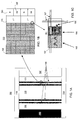
FIG. 1B is an expanded view of the hybridprogrammable logic device 100 containingprocessors 150 adjacent toprogrammable logic elements 130 in accordance with an embodiment of the present invention. Two processors are depicted schematically inFIG. 1B as squares containing three components -processor core 170,instruction cache 180, anddata cache 190. Also depicted schematically inFIG. 1B areprogrammable logic elements 130 that are grouped intoLABs 132. In certain embodiments, the physical size of a dimension of theprocessors 150, such as length, height, or width, is a multiple of the same dimension of theprogrammable logic elements 150, or LABs made up ofprogrammable logic elements 150. For example, as depicted inFIG. 1B , the width of each of the two processors is equal to threeLABs 132. This allows for efficient assembly of devices having different dimensions, with differing ratios of processors to programmable logic elements or other logic blocks. -
FIG. 1C is an expanded view of the hybridprogrammable logic device 100 containing aninterface 161 between theprocessors 150 andprogrammable logic elements 130 in accordance with an embodiment of the present invention.Interface 161 may be included between every LAB or row of LABs andprocessors 150.Interface 161 may include LIM /LEIM circuitry 162,interface logic 164, andinterface port 166. LIM /LEIM circuitry 162 refers to collections of programmable input muxes "LAB Input Mux" and "Logic Element Input Mux," and may include any suitable number of LIM and LEIM multiplexors as commonly found in devices sold by Altera Corporation of San Jose, California.Interface logic 164 may include any suitable circuit components for buffering data to interfaceport 166.Interface port 166 may include any suitable circuitry for physically delivering signals to one ofprocessors 150. - In certain embodiments, horizontal and
vertical connectors 167 may also be included ondevice 100. As will be discussed below with respect toFIG. 3 , horizontal andvertical connectors 167 may transfer data betweenprocessors 150,programmable logic elements 120, general input / output interfaces, and memory on and off chip. In certain embodiments, horizontal and vertical connectors may be wired tointerface circuitry 161 such that any signal from any of theprogrammable logic elements 130 can be delivered tointerface port 166 via LIM /LEIM circuitry 162 andinterface logic 164. For example, multiplexors within the LIM /LEIM circuitry 162 may choose which signal drives any global wire in the horizontal /vertical connectors 167 to connect any of theprogrammable logic elements 130 withprocessors 150. -
FIG. 2A is an illustrative view of thedata bus 210 in the hybridprogrammable logic device 100 in accordance with an embodiment of the present invention. Although the wires ofdata bus 210 are shown above theLABs 215 in the vertical direction, in implementation they are part of an interconnect stack which is above the LABs (e.g., in a metal layer above the metal layers containing the LABs and processors). Similar to horizontal andvertical connectors 167,data bus 210 can transfer data betweenprocessors 150,programmable logic elements 130, general input /output interfaces 110, and memory on and off the device 100 (FIG. 1A ).FIG. 2A illustratively highlights two wires ofdata bus 210 routed fromLAB 216 of a particular spacing aboveLABs 215. In certain embodiments, the horizontal and vertical connectors ofdata bus 210 may be laid out such that their vertical pitch (e.g., vertical position in the interconnect stack, illustrated by 'W' inFIG. 2A and 2B ) is a multiple of the size (e.g., the vertical pitch) of one or more groups of programmable logic elements, processors, or both. -
FIG. 2B is another illustrative view of thedata bus 210 in the hybridprogrammable logic device 100 in accordance with an embodiment of the present invention. As depicted schematically inFIG. 2B ,processor 217 is in place ofLAB 216.Processor 217 may be part of a column of tiled processors in the device, such as one of tiled processors 150 (FIG. 1A ). In certain embodiments, the wiring ofdata bus 210 has the same vertical pitch and follows the same pattern of the wiring ofdata bus 210 toLABs 215 andLAB 216. In addition, in certain embodiments, both the wiring fromprocessor 217 andLABs 215 andLAB 216 are in the same metal layer in the interconnect stack (e.g., in a metal layer above the metal layers containing the LABs and processors). By placing the horizontal and vertical connectors for both the processor and programmable logic elements in the same metal layer, and sizing them such that they agree with the size (e.g., vertical pitch) of the programmable logic elements and processors, allows for place and route tools (e.g., software) to address the processors and logic elements as a homogenous routing fabric. In other words, portions of the connectors that route data to and from the processors (such as processor 217) may be addressed in the same manner as the connectors that route data to and from the programmable logic elements (such as the programmable logic elements inLABs 215 and LAB 216). -
FIG. 3 is a hybridprogrammable logic device 300 with ahardened data bus 160 and ingress / egress processing block 136 in accordance with an embodiment of the present invention.FIG. 4A is the same hybridprogrammable logic device 300 with a differenthardened data bus 160 in accordance with an embodiment of the present invention.FIG. 4B is the same hybridprogrammable logic device 300 with another differenthardened data bus 160. -
Device 300 also includesexternal memory 135 and embedded ternary-content addressable memory (CAM) memory 137.Hardened data bus 160 may consist of dedicated circuit components that transfer data to and fromprocessors 150,programmable logic elements 130, ingress / egress processing block 136,external memory 135, and embedded ternary-CAM memory 137, rather than being reserved for other uses on the device. In certain embodiments,hardened data bus 160 may be referred to as a network on chip interconnect. In such embodiments,hardened data bus 160 may be dedicated to routing and / or carrying the data to and from the ingress / egress processing block to other elements of the device.Hardened data bus 160 can allow for high performance data transfer both internal and external to the device. In certain embodiments,hardened data bus 160 may include a portion of horizontal and vertical connectors 167 (FIG. 1C ) and data bus 210 (FIGs. 2A and 2B ). In other embodiments,hardened data bus 160 may be entirely separate from horizontal andvertical connectors 167. -
Hardened data bus 160 may have a variety of topologies. For example,hardened data bus 160 may have a ring topology, a shared bus protocol such as AXI designed by ARM holdings of Cambridge, United Kingdom, interconnect technology from Sonics, Arteris or other third party companies, or Avalon interconnect designed by Altera Corporation of San Jose, California. In certain embodiments,hardened data bus 160 may be hierarchical. For example, as depicted schematically inFIG. 3 ,hardened data bus 160 may be a 4-way division. In another example, as depicted schematically inFIG. 4A ,hardened data bus 160 may be monolithic. In yet another example, as depicted schematically inFIG. 4B , hardened data bus may be segmented. - In certain embodiments, portions of
hardened data bus 160 may be connected or disconnected hierarchically by software that can programdevice 300. This software may include Quartus software design by Altera Corporation of San Jose, California, or any other suitable software. In certain embodiments, the bandwidth ofhardened data bus 160 is designed to achieve the line-rate of a particular application. For example, ifhardened data bus 160 is 64 bits and operating at 1 GHz with 80% efficiency, it can provide 51Gbps of bandwidth and be used to target a 50Gbps streaming video application. In another example, ifhardened data bus 160 is 64 bits and operating at 1.5 GHz with 80% efficiency, it can provide 150Gbps of bandwidth and target an 100Gb traffic switch application. In certain embodiments, separate hardened data buses may be added to carry data for processor input and output, as LAB input and output. - In certain embodiments,
hardened data bus 160 may be placed over (e.g., in a metal layer above) or adjacent toprocessors 150 andprogrammable logic elements 130. In this manner,hardened data bus 160 is minimally invasive to the assembly of device 300 (FIG. 3 ). -
External memory 135 may include any suitable interface to external memory, such as DDR memory.External memory 135 can buffer data in applications wheredevice 300 is processing video data or packet data. In certain embodiments, embedded ternary-CAM memory 137 may include any suitable block of content addressable memory, which is useful for networking applications. In certain embodiments, embedded ternary-CAM memory 137 may interface withprogrammable logic elements 130 andprocessors 150 using circuitry substantially similar to interface circuitry 161 (FIG. 1C ). In certain embodiments, ternary-CAM memory 137 may be replaced by an SRAM or embedded SRAM packet buffer memory. - Ingress / egress processing block 136 can receive data and forward that data to other elements of
device 300. For example, ingress / egress processing block 136 can receive data packets and provide protocol termination or packet framing services todevice 300. In certain embodiments, ingress / egress processing block 136 may forward received data tohardened data bus 160. In certain embodiments, the ingress / egress processing block may consist of hardened ASIC blocks. These blocks may be structured according to the ASIC blocks disclosed inU.S. Patent No. 8,314,636 , which is incorporated by reference herein in its entirety. In certain embodiments, ingress / egress processing block may be built fromprogrammable logic elements 130. -
FIG. 5 is a hybridprogrammable logic device 500 with ahardened data bus 160 and ingress / egress 137 in accordance with yet another embodiment of the present invention.Device 500 may be substantially similar to device 100 (FIG. 1A ) and device 300 (FIG. 3 ), except that a universal interface bus 138 is integrated intodevice 500 for interfacing to 2.5D or 3D memory, or other functions. As schematically illustrated inFIG. 5 , interface 138 can be connected toprocessors 150 andprogrammable logic elements 130 via hardeneddata bus 160. In other embodiments, interface 138 can be connected toprocessors 150 andprogrammable logic elements 130 through general-purpose FPGA routing, such as horizontal and vertical connectors 167 (FIG. 1C ). In certain embodiments, interface 138 may be manufactured according to the design and methods described inU.S. Patent Application Nos. 13/350,662 and13/620,126 -
FIG. 6 is schedulingcircuitry 600 in accordance with an embodiment of the present invention.Scheduling circuitry 600 includesdata bus 605, which can be substantially similar to horizontal and vertical connectors 167 (FIG. 1C ), or hardened data bus 160 (FIG. 3 ).Scheduling circuitry 600 can schedule the transmission of data on the horizontal and vertical connectors, hardened data bus, between programmable logic elements such asprogrammable logic elements 130 andprocessor 630. In certain embodiments,processor 630 may be part of a column of tiled processors, such as those described with respect to processors 150 (FIG. 1A ). In such embodiments, copies ofscheduling circuitry 600 may be integrated with every processor inprocessors 150. -
Scheduling circuitry 600 includesbus interface 610 and threadingcircuitry 620. In certain embodiments, scheduling circuitry may also includeprocessor 630 andcache 640.Processor 630 may be substantially similar to processors 150 (FIG. 1A ), andcache 640 may be substantially similar toinstruction cache 180 anddata cache 190. In addition,processor 630 may be part of a tiled column or row of processors, such as that discussed with respect to processors 150 (FIG. 1A ). In such embodiments,scheduling circuitry 600 may be implemented on the device for every processor in the tiled rows or columns of processors. - Horizontal and
vertical connectors 605 may transmit data to and frombus interface 610. Horizontal andvertical connectors 605 may be part of at least a portion of horizontal andvertical connectors 167,hardened data bus 160, or both. In certain embodiments,bus interface 210 may transmit data to and from programmable logic elements on a device and processors on a device using horizontal andvertical connectors 605. For example,bus interface 210 may transmit data betweenprogrammable logic elements 130 ofdevice 100 andprocessor 630 using horizontal andvertical connectors 167. In certain embodiments, the transmission of data between the programmable logic elements and the processors may occur at a rate of speed different, or asynchronous from, the rate of speed of the clock ofprocessor 630. For example, the speed of the operation of the processor may be faster or slower than the speed of operation of the programmable logic elements on the device, and the rate of speed at which data is transmitted between the programmable logic elements and processor using horizontal andvertical connectors 605 may be different than the speed of the clock ofprocessor 630. - In such embodiments,
bus interface 610 may provide mechanisms that allow data to be transmitted on the horizontal andvertical connectors 605 at a rate asynchronous with respect to the speed of the clock ofprocessor 630. In certain embodiments,bus interface 610 may receive interrupt messages over horizontal andvertical connectors 605. In such embodiments, these interrupt messages may be addressed to one or more of the processors on the device, meaning that they contain information that indicate that the payload of the data associated with the messages is meant to be processed by a particular processor or processors.Bus interface circuitry 610 may transmit only the data associated with interrupt messages that are addressed toprocessor 630, and ignore other messages that are not addressed toprocessor 630. For example,bus interface circuitry 610 may contain a predetermined or hardcoded value, either in software or hardware associated withbus circuitry 610, that is the address ofprocessor 630.Bus interface circuitry 610 may periodically or constantly monitor the messages transmitted over horizontal andvertical connectors 605 for the address. When the address is detected,bus interface circuitry 610 may buffer data associated with the message addressed toprocessor 630, and transmit the data from the buffer toprocessor 630 usingthreading circuitry 620.Threading circuitry 620 maintains one or more program counters associated with the execution of various tasks inprocessor 630. In certain embodiments, threadingcircuitry 620 receives data frombus interface circuitry 610, and determines the appropriate time to send that data toprocessor 630 based on one or more of the program counters that it maintains. In this manner,scheduling circuitry 600 may allow the processors, programmable logic elements, and the data bus of a device to operate at different clock speeds, thus breaking any timing or clock dependency between the components tied to the network bus and the processor clock speed. - In certain embodiments, any suitable methods of asynchronous communication may be used to send data between the programmable logic elements of the device and
processor 630. In certain embodiments, the functionality ofscheduling circuitry 600 may be achieved by groups of two or more processors rather than schedulingcircuitry 600. These groups of processors may identify which of the processors to send data received from the horizontal and vertical conductors of the device (i.e., transmitted from the programmable logic elements), and distribute the data to the identified processors. This identification may be determined similar to the monitoring procedure described above with respect tobus interface circuitry 610. - In certain embodiments,
scheduling circuitry 600 may include a program instruction memory (not shown), which can include any suitable combination of external memory. In certain embodiments, the instruction set of the processors on the device, such asprocessor 630, may be modified during operation such that they are reprogrammed with a new instruction set. This new instruction set may allow the device to achieve new or different functionality, such as program instructions for a hardware accelerator that may be used by the processors. - In such embodiments, the program instruction memory may detect a new mode of operation for one or more of the processors. For example, the program instruction memory may contain instructions for monitoring data packets on the horizontal and
vertical connectors 605. Certain data packets, which can be identified by their packet header, may contain a control packet that contains instructions for reprogrammingprocessor 630 with new or updated functionality.Bus interface circuitry 610 may detect these control packets by monitoring horizontal and vertical connectors periodically or continuously to match the control packet headers. In response to the detection of a new mode of operation, the operation ofprocessor 630 may be halted. For example, oncebus interface circuitry 610 detects a control packet header, it may buffer the payload data of that packet and transfer the payload data to threadingcircuitry 620.Threading circuitry 620 may then perform one or more of the creation, execution, or insertion instructions in the threads or pipeline ofprocessor 630 that causeprocessor 630 to halt operation, and flush out all pending instructions.Threading circuitry 620 may then transfer the payload of the control packet that contains the instructions for reprogrammingprocessor 630 from a buffer inbus interface circuitry 610 toprocessor 630. In certain embodiments, information in the header of the control packet may target a group of processors, such as a group of processors in one or more tiled columns on the device. In such embodiments, the process described above may occur substantially in parallel for each of the targeted processors on the device using each processor's associated bus interface circuitry. - In certain embodiments, the processors on the device may be divided into different classes via partitioning. This partitioning may be physical (e.g., hard-coded in the processor), or virtual (e.g., assigned via a record kept by scheduling software)
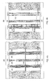
FIG. 7A is an illustration of a partitioned hybridprogrammable logic device 100 in accordance with an embodiment of the present invention.Device 100 may be substantially similar to that described with respect toFIG. 1A .Device 100 may be partitioned into afirst partition 702,second partition 704, andthird partition 706. These partitions may be designated by place and route tools, or any suitable software. In certain embodiments, the partitions may be designated by a table that maps each of the processor's addresses or other unique identifiers with a partition number. In certain embodiments, the partitions of processors may also be associated with a partition of the programmable logic elements ofdevice 100. It shall be understood that whileFIG. 7A shows three partitions, the processors ondevice 100 may be divided into any suitable number of partitions in any suitable geometry on the device. - Each
partition first partition 702 may be designated to handle flow identification processing, the processors associated withsecond partition 704 may be designated to handle initial packet processing and distribution, and the processors associated withthird partition 706 may be designated to handle system or device-wide state processing. In this manner,device 100 may be configured to handle any number of applications. The use ofdevice 100 in packet processing applications is further illustrated and discussed inU.S. Patent Application No. 13/826,039 , which is incorporated by reference herein in its entirety. - In certain embodiments, the different classes of processors and programmable logic elements may be used to manage power usage of
device 100. For example, processors and programmable logic elements associated with partitions ofdevice 100 may be powered up and down dynamically based on the demand for the processing capabilities of the processors and logic elements associated with each partition. This process is described with respect toFIG. 7B below. - In certain embodiments, processors and programmable logic elements associated with one or more partitions of
device 100 may be designated as housekeeper processors. These housekeeper processors may implement functions such as power and clock management on behalf ofdevice 100. In certain embodiments, these housekeeper processors may be designated by the user of place and route tools. In other embodiments, these housekeeper processors may be designated bydevice 100 automatically during runtime ofdevice 100. -
FIG. 7B is anillustrative process 700 for reducing power consumption of a hybrid programmable logic device, such as device 100 (FIGs. 1A and7A ), in accordance with an embodiment of the present invention.Process 700 begins atstep 710. Atstep 710, at least two partitions of the device are computed, each partition including processors associated with programmable logic elements. Each of these two partitions may be substantially similar topartitions FIG. 7A . In certain embodiments, the partitions may be computed by place and route software before operation of the device. In other embodiments, the partitions may be computed by scheduling software during the operation of the device. This scheduling software may be executed on a host processor external to the device, or on designated housekeeper processors. In such embodiments, the scheduling software may change the partitions dynamically during the operation of the device. For example, at a first time the scheduling software may designate a first partition associated with 40% of the processors and associated programmable logic elements that are actively being used for hardware acceleration functions, and a second partition associated with 60% of the processors and associated programmable logic elements that are not actively being used. Then, at a subsequent time, after more of the processors and programmable logic elements have become active, the scheduling software may designate a first partition associated with 55% of the processors and programmable logic elements that are actively being used for hardware acceleration, and a second partition associated with 45% of the processors and associated programmable logic elements that are not actively being used. In this manner, the device can actively adjust its power usage based on throughput of the device. In certain embodiments, the partitions may be associated with a "top half" and "bottom half" of the processors and associated programmable logic elements. In such embodiments, scheduling software may designate the partition associated with the "bottom half" of the resources in the device in a power savings mode while the partition associated with the "top half" of the resources in the device may be designated for an active mode. In certain embodiments, the partitions may be computed by determining what hardware acceleration functions are being executed by a processor or group of processors, and then designating those processors and the programmable logic elements associated with executing a particular hardware acceleration function as a single partition. -
Process 700 may proceed to step 720. Atstep 720, at least one measure of processor demand is computed. In certain embodiments, these measures of processor demand may be computed for each partition computed atstep 710. In certain embodiments, a measure of processor demand may be computed by the scheduling software. In certain embodiments, the measure of processor demand may be computed by determining the number of received data packets that are waiting (e.g., in a queue) to be processed by a processor or a group of processors (e.g., all of the processors in a particular partition). In one embodiment, if a processor or group of processors have not received data packets for a predetermined period of time (e.g., because the processors and associated programmable logic elements perform a hardware acceleration function that is not being used), the processor or group of processors may be designated as unneeded, and marked for powering down as will be discussed with respect to step 730 below. In this manner, processors which are no longer needed for their processing power are figuratively "laid off" from performing their job ondevice 100. In the same embodiment, if data packets are subsequently received for the processor or group of processors marked as idle, those data packets may be queued and the processor or processors may be designated as active and marked for powering on as will be discussed with respect to step 730 below. In this manner, idle processors which are needed again are figuratively hired back to performing their job ondevice 100. In another embodiment, if a processor or group of processors have received a number of data packets below a predetermined threshold, the processor or group of processors may be designated as unneeded, and marked for powering down as will be discussed with respect to step 730 below. -
Process 700 may then proceed to step 730. Atstep 730, the power state of the processors and associated programmable logic blocks in the partitions may be altered based on the measure of processor demand computed atstep 720. In certain embodiments, the power state of a partition may be altered by powering down the resources of the device allocated to that partition. For example, if processor demand is calculated for a particular partition as being less than a threshold number of received data packets, then the processors or groups of processors and associated programmable logic elements of that partition may be powered down. In certain embodiments, resources within a partition may be powered down by disabling the clock signal provided to those resources. In certain embodiments, the power state of a partition may be altered by powering up the resources of a partition that was previously powered down or is dormant. For example, if the device determines that the resources in a particular partition that is powered down are needed to execute a new or scheduled hardware acceleration function, or that data packets are currently being received that call for resources associated with a hardware acceleration function that were previously powered down, then the resources within that partition may be powered up. In certain embodiments, resources within a partition may be powered up by enabling the clock signal provided to those resources. -
Additional embodiment 1 provides a hybrid programmable logic device, comprising programmable logic elements, at least some of which provide at least one hardware acceleration function; processors interleaved with the programmable logic elements and physically sized such that one physical dimension of each of the processors is equal to a multiple of a same physical dimension of the programmable logic elements; and first horizontal and vertical connectors that provide data to and from the programmable logic elements; and second horizontal and vertical connectors that provide data to and from the processors. - According to additional embodiment 2, each of the processors of the device of
additional embodiment 1 consists of fixed logic elements. - According to additional embodiment 3, the first and second horizontal and vertical connectors of the device of
additional embodiment 1 are in a same metal layer of the hybrid programmable logic device. - According to additional embodiment 4, the processors of the device of
additional embodiment 1 are arranged in one of columns or rows. - According to additional embodiment 5, the physical dimension is one of length, width, or height.
- According to additional embodiment 6, the first and second horizontal and vertical connectors of the device of
additional embodiment 1 are addressable as a homogeneous routing fabric to provide data to and from the processors and programmable logic elements. - According to additional embodiment 7, the first and second horizontal and vertical connectors of the device of
additional embodiment 1 only provide data to and from the processors and programmable logic elements. - According to additional embodiment 8, the device of additional embodiment 7 further comprises an ingress / egress processing block that receive data packets and route them to the first and second horizontal vertical connectors.
- According to additional embodiment 9, the device of additional embodiment 8 further comprises an external memory configured directly connected to the hybrid programmable logic device, wherein the external memory buffers the received data packets.
- According to additional embodiment 10, the device of additional embodiment 8 further comprises a network on chip bus, operable only to carry the data packets to and from the ingress / egress processing block.
- According to additional embodiment 11, wherein the ingress / egress processing block of the device of additional embodiment 8 consists of at least one of a dedicated ASIC, or a group of the programmable logic elements.
- According to
additional embodiment 12, the device of additional embodiment 3 further comprises a first metal layer containing the programmable logic elements and processors, wherein the first metal layer is distinct from the same metal layer. - According to additional embodiment 13,wherein the programmable logic elements of the device of
additional embodiment 1 change the at least one hardware acceleration function. - Additional embodiment 14 provides a hybrid programmable logic device, comprising programmable logic elements that operate at a first clock speed, wherein at least some of which provide at least one hardware acceleration function; processors interleaved with the programmable logic elements that operate at a second clock speed asynchronous with respect to the first clock speed, wherein each of the processors consists of fixed logic elements; and horizontal and vertical connectors that provide data between the programmable logic elements and processors; and scheduling circuitry that transmits data on the horizontal and vertical and vertical connectors between the programmable logic elements and processors at a rate asynchronous with respect to the second clock speed.
- According to additional embodiment 15, the scheduling circuitry of the device of additional embodiment 14 receives interrupt messages addressed to at least one of the processors.
- According to additional embodiment 16, where a group of the processors of the device of additional embodiment 14 comprise circuitry that processes data transmitted between the programmable logic elements and processors to identify which of the processors to send the data; and distribute the data to the identified processors.
- According to additional embodiment 17, the scheduling circuitry of the processors of the device of additional embodiment 14 further comprises a program instruction memory that contains a program instruction set that detects a new mode of operation for a group of the processors; in response to the detection of a new mode of operation, halts operation of the processors in the group; and receives data from the programmable logic elements; and stores instructions in the program instruction memory based on the received data.
- Additional embodiment 18 provides a method of initializing and operating a hybrid programmable logic device comprising processors interleaved with the programmable logic elements, the method comprising computing at least two partitions of the hybrid programmable logic device, wherein each partition comprises a subset of the processors and the programmable logic elements; computing at least one measure of processor demand for each of the at least two partitions; and based on the computed measure of processor demand, altering the power state of the processors and programmable logic elements in at least one of the at least two partitions.
- According to additional embodiment 19, in the method of additional embodiment 18, altering the power state of the processors and programmable logic devices consists of one of disabling clock circuitry associated with the processors and programmable logic elements, or powering down the processors and programmable logic circuits.
- According to additional embodiment 20, in the method of additional embodiment 18, computing the measure of processor demand further comprises computing a number of received data packets designated for the processors in each of the partitions of the hybrid FPGA device; and determining whether the number of received data packets is below a predetermined threshold.
- According to additional embodiment 21, in the method of additional embodiment 18, computing measure of processor demand further comprises determining that data packets have not been received by the processors in a partition of the FPGA device for a predetermined period of time.
- According to additional embodiment 22, in the method of additional embodiment 18, computing at least two partitions of the hybrid FPGA device comprise determining hardware acceleration functions used by the processors; and based on the determination, generating a partition that includes the processors and programmable logic elements associated with the hardware acceleration functions.
- It will be understood that the foregoing is only illustrative of the principles of the invention, and that various modifications can be made by those skilled in the art. One skilled in the art will appreciate that the present invention can be practiced by other than the described embodiments, which are presented for purposes of illustration and not of limitation, and the present invention is limited only by the claims that follow.
Claims (17)
- A hybrid programmable logic device, comprising:programmable logic elements, at least some of which provide at least one hardware acceleration function;processors interleaved with the programmable logic elements and physically sized such that one physical dimension of each of the processors is equal to a multiple of a same physical dimension of the programmable logic elements; andfirst horizontal and vertical connectors that provide data to and from the programmable logic elements; andsecond horizontal and vertical connectors that provide data to and from the processors.
- The device of claim 1, wherein each of the processors consists of fixed logic elements.
- The device of claim 1 or 2, wherein the first and second horizontal and vertical connectors are in a same metal layer of the hybrid programmable logic device.
- The device of one of claims 3, further comprising a first metal layer containing the programmable logic elements and processors, wherein the first metal layer is distinct from the same metal layer.
- The device of one of claims 1 to 4, wherein the processors are arranged in one of columns or rows.
- The device of one of claims 1 to 5, wherein the first and second horizontal and vertical connectors are addressable as a homogeneous routing fabric to provide data to and from the processors and programmable logic elements.
- The device of one of claims 1 to 6, wherein the first and second horizontal and vertical connectors only provide data to and from the processors and programmable logic elements.
- The device of claim 7, further comprising an ingress/egress processing block that receive data packets and route them to the first and second horizontal vertical connectors.
- The device of claim 8, further comprising an external memory configured directly connected to the hybrid programmable logic device, wherein the external memory buffers the received data packets.
- The device of claim 8 or 9, further comprising a network on chip bus, operable only to carry the data packets to and from the ingress/egress processing block.
- The device of one of claims 8 to 10, wherein the ingress/egress processing block consists of at least one of a dedicated ASIC, or a group of the programmable logic elements.
- The device of one of claims 1 to 11, wherein the programmable logic elements change the at least one hardware acceleration function.
- A method of initializing and operating a hybrid programmable logic device comprising processors interleaved with the programmable logic elements, the method comprising:computing at least two partitions of the hybrid programmable logic device, wherein each partition comprises a subset of the processors and the programmable logic elements;computing at least one measure of processor demand for each of the at least two partitions; andbased on the computed measure of processor demand, altering the power state of the processors and programmable logic elements in at least one of the at least two partitions.
- The method of claim 13 wherein altering the power state of the processors and programmable logic devices consists of one of disabling clock circuitry associated with the processors and programmable logic elements, or powering down the processors and programmable logic circuits.
- The method of claim 13 or 14, wherein computing the measure of processor demand further comprises:computing a number of received data packets designated for the processors in each of the partitions of the hybrid FPGA device; anddetermining whether the number of received data packets is below a predetermined threshold.
- The method of one of claims 13 to 15, wherein computing measure of processor demand further comprises
determining that data packets have not been received by the processors in a partition of the FPGA device for a predetermined period of time. - The method of one of claims 13 to 16, wherein computing at least two partitions of the hybrid FPGA device comprise:determining hardware acceleration functions used by the processors; andbased on the determination, generating a partition that includes the processors and programmable logic elements associated with the hardware acceleration functions.
Applications Claiming Priority (1)
| Application Number | Priority Date | Filing Date | Title |
|---|---|---|---|
| US13/804,419 US9471537B2 (en) | 2013-03-14 | 2013-03-14 | Hybrid programmable many-core device with on-chip interconnect |
Publications (2)
| Publication Number | Publication Date |
|---|---|
| EP2778946A2 true EP2778946A2 (en) | 2014-09-17 |
| EP2778946A3 EP2778946A3 (en) | 2016-01-13 |
Family
ID=50289371
Family Applications (1)
| Application Number | Title | Priority Date | Filing Date |
|---|---|---|---|
| EP14158110.8A Ceased EP2778946A3 (en) | 2013-03-14 | 2014-03-06 | Hybrid programmable many-core device with on-chip interconnect |
Country Status (3)
| Country | Link |
|---|---|
| US (5) | US9471537B2 (en) |
| EP (1) | EP2778946A3 (en) |
| CN (2) | CN104050142B (en) |
Cited By (1)
| Publication number | Priority date | Publication date | Assignee | Title |
|---|---|---|---|---|
| WO2020197803A1 (en) * | 2019-03-27 | 2020-10-01 | Xilinx, Inc. | Adaptive integrated programmable device platform |
Families Citing this family (14)
| Publication number | Priority date | Publication date | Assignee | Title |
|---|---|---|---|---|
| US9258273B2 (en) * | 2013-10-03 | 2016-02-09 | Mcafee, Inc. | Duplicating packets efficiently within a network security appliance |
| CN105632567B (en) * | 2014-10-27 | 2019-01-01 | 阿尔特拉公司 | Integrated circuit device with embedded programmable logic |
| CN104636311A (en) * | 2015-02-28 | 2015-05-20 | 天津大学 | Method for developing sizes of multiprocessor system-on-chip network interconnection arrays |
| US10606779B2 (en) | 2016-09-16 | 2020-03-31 | Altera Corporation | Methods and apparatus for performing partial reconfiguration in a pipeline-based network topology |
| US10416974B2 (en) | 2017-10-06 | 2019-09-17 | Chicago Mercantile Exchange Inc. | Dynamic tracer message logging based on bottleneck detection |
| US11296706B2 (en) | 2018-06-27 | 2022-04-05 | Intel Corporation | Embedded network on chip accessible to programmable logic fabric of programmable logic device in multi-dimensional die systems |
| US10838909B2 (en) * | 2018-09-24 | 2020-11-17 | Hewlett Packard Enterprise Development Lp | Methods and systems for computing in memory |
| KR102669395B1 (en) | 2018-10-04 | 2024-05-29 | 삼성디스플레이 주식회사 | Connector assembly and display apparatus having the same |
| CN112486895B (en) * | 2019-09-12 | 2024-01-09 | 阿里巴巴集团控股有限公司 | An FPGA chip and its interconnection control method |
| CN112817905A (en) * | 2021-02-05 | 2021-05-18 | 中国电子科技集团公司第五十八研究所 | Interconnection bare chip, interconnection micro assembly, interconnection micro system and communication method thereof |
| CN113704169B (en) * | 2021-08-12 | 2024-05-28 | 北京时代民芯科技有限公司 | A configurable many-core processor for embedded systems |
| CN116226023B (en) | 2021-12-02 | 2026-07-31 | 平头哥(上海)半导体技术有限公司 | Parallel processing unit, processing system and related method |
| CN116561047A (en) | 2022-01-28 | 2023-08-08 | 阿里巴巴(中国)有限公司 | Processing system and communication method for inter-chip communication |
| CN116701292A (en) | 2022-02-24 | 2023-09-05 | 平头哥(上海)半导体技术有限公司 | Processing system and communication method for inter-chip communication |
Citations (3)
| Publication number | Priority date | Publication date | Assignee | Title |
|---|---|---|---|---|
| US7132851B2 (en) * | 2003-07-11 | 2006-11-07 | Xilinx, Inc. | Columnar floorplan |
| US7315918B1 (en) * | 2005-01-14 | 2008-01-01 | Xilinx, Inc. | Processor block placement relative to memory in a programmable logic device |
| US8314636B2 (en) | 2007-08-20 | 2012-11-20 | Altera Corporation | Field programmable gate array with integrated application specific integrated circuit fabric |
Family Cites Families (25)
| Publication number | Priority date | Publication date | Assignee | Title |
|---|---|---|---|---|
| US7356620B2 (en) | 2003-06-10 | 2008-04-08 | Altera Corporation | Apparatus and methods for communicating with programmable logic devices |
| US6557096B1 (en) | 1999-10-25 | 2003-04-29 | Intel Corporation | Processors with data typer and aligner selectively coupling data bits of data buses to adder and multiplier functional blocks to execute instructions with flexible data types |
| US7123623B2 (en) | 2000-11-29 | 2006-10-17 | Tellabs Operations, Inc. | High-speed parallel cross bar switch |
| US6917589B2 (en) | 2001-01-25 | 2005-07-12 | Agere Systems Inc. | Automatic quality of service assignment in ethernet switches |
| US6781407B2 (en) | 2002-01-09 | 2004-08-24 | Xilinx, Inc. | FPGA and embedded circuitry initialization and processing |
| US6798239B2 (en) | 2001-09-28 | 2004-09-28 | Xilinx, Inc. | Programmable gate array having interconnecting logic to support embedded fixed logic circuitry |
| US8914590B2 (en) * | 2002-08-07 | 2014-12-16 | Pact Xpp Technologies Ag | Data processing method and device |
| US7200735B2 (en) * | 2002-04-10 | 2007-04-03 | Tensilica, Inc. | High-performance hybrid processor with configurable execution units |
| US20050249185A1 (en) | 2002-06-07 | 2005-11-10 | Poor Robert D | Routing in wireless networks |
| US20110238948A1 (en) * | 2002-08-07 | 2011-09-29 | Martin Vorbach | Method and device for coupling a data processing unit and a data processing array |
| US7657861B2 (en) * | 2002-08-07 | 2010-02-02 | Pact Xpp Technologies Ag | Method and device for processing data |
| US6754744B2 (en) | 2002-09-10 | 2004-06-22 | Broadcom Corporation | Balanced linked lists for high performance data buffers in a network device |
| US7092975B2 (en) | 2003-02-12 | 2006-08-15 | Ge Mortgage Holdings, Llc | Methods and apparatus for management of data storage resources |
| US6803786B1 (en) * | 2003-03-11 | 2004-10-12 | Xilinx, Inc. | Structures and methods providing columns of tightly coupled processor and RAM blocks within an array of logic blocks |
| US7157934B2 (en) * | 2003-08-19 | 2007-01-02 | Cornell Research Foundation, Inc. | Programmable asynchronous pipeline arrays |
| CA2544411A1 (en) | 2003-10-30 | 2005-05-26 | Venkat Konda | Nonblocking and deterministic multirate multicast packet scheduling |
| US7064580B2 (en) * | 2004-07-22 | 2006-06-20 | Altera Corporation | Mask-programmable logic device with programmable portions |
| US7551617B2 (en) | 2005-02-08 | 2009-06-23 | Cisco Technology, Inc. | Multi-threaded packet processing architecture with global packet memory, packet recirculation, and coprocessor |
| US7814242B1 (en) | 2005-03-25 | 2010-10-12 | Tilera Corporation | Managing data flows in a parallel processing environment |
| US7746862B1 (en) | 2005-08-02 | 2010-06-29 | Juniper Networks, Inc. | Packet processing in a multiple processor system |
| US8761188B1 (en) * | 2007-05-01 | 2014-06-24 | Altera Corporation | Multi-threaded software-programmable framework for high-performance scalable and modular datapath designs |
| CN102331733A (en) * | 2010-07-14 | 2012-01-25 | 中国科学院沈阳计算技术研究所有限公司 | Numerical control system logic controller on basis of system on programmable chip and implementing method thereof |
| CN101902321B (en) * | 2010-08-13 | 2014-11-05 | 中兴通讯股份有限公司 | Clock management method and system |
| US8667192B2 (en) * | 2011-02-28 | 2014-03-04 | Xilinx, Inc. | Integrated circuit with programmable circuitry and an embedded processor system |
| US8769477B1 (en) * | 2013-01-31 | 2014-07-01 | Xilinx, Inc. | Computer aided design tool and user interface for configuration of a programmable system-on-a-chip |
-
2013
- 2013-03-14 US US13/804,419 patent/US9471537B2/en active Active
-
2014
- 2014-03-06 EP EP14158110.8A patent/EP2778946A3/en not_active Ceased
- 2014-03-13 CN CN201410092909.4A patent/CN104050142B/en active Active
- 2014-03-13 CN CN201811237154.7A patent/CN109634909B/en active Active
-
2016
- 2016-10-07 US US15/288,569 patent/US9830300B2/en active Active
-
2017
- 2017-11-27 US US15/823,353 patent/US10127190B2/en active Active
-
2018
- 2018-11-09 US US16/186,248 patent/US10635631B2/en active Active
-
2020
- 2020-04-27 US US16/859,728 patent/US11256656B2/en active Active
Patent Citations (3)
| Publication number | Priority date | Publication date | Assignee | Title |
|---|---|---|---|---|
| US7132851B2 (en) * | 2003-07-11 | 2006-11-07 | Xilinx, Inc. | Columnar floorplan |
| US7315918B1 (en) * | 2005-01-14 | 2008-01-01 | Xilinx, Inc. | Processor block placement relative to memory in a programmable logic device |
| US8314636B2 (en) | 2007-08-20 | 2012-11-20 | Altera Corporation | Field programmable gate array with integrated application specific integrated circuit fabric |
Non-Patent Citations (1)
| Title |
|---|
| XILINX INC.: "Virtex-II Pro and Virtex-II Pro X Platform FPGAs: Complete Data Sheet", 21 June 2011 (2011-06-21), pages 1, 12, XP055760618, Retrieved from the Internet <URL:https://www.xilinx.com/support/documentation/data_sheets/ds083.pdf> [retrieved on 20201216] * |
Cited By (6)
| Publication number | Priority date | Publication date | Assignee | Title |
|---|---|---|---|---|
| WO2020197803A1 (en) * | 2019-03-27 | 2020-10-01 | Xilinx, Inc. | Adaptive integrated programmable device platform |
| US11063594B1 (en) | 2019-03-27 | 2021-07-13 | Xilinx, Inc. | Adaptive integrated programmable device platform |
| KR20210143745A (en) * | 2019-03-27 | 2021-11-29 | 자일링크스 인코포레이티드 | Adaptive Integrated Programmable Device Platform |
| JP2022527760A (en) * | 2019-03-27 | 2022-06-06 | ザイリンクス インコーポレイテッド | Adaptive integrated programmable device platform |
| US11683038B1 (en) | 2019-03-27 | 2023-06-20 | Xilinx, Inc. | Adaptive integrated programmable device platform |
| US12261603B2 (en) | 2019-03-27 | 2025-03-25 | Xilinx, Inc. | Adaptive integrated programmable device platform |
Also Published As
| Publication number | Publication date |
|---|---|
| US9830300B2 (en) | 2017-11-28 |
| US11256656B2 (en) | 2022-02-22 |
| CN104050142B (en) | 2018-11-16 |
| EP2778946A3 (en) | 2016-01-13 |
| US20190121783A1 (en) | 2019-04-25 |
| US10635631B2 (en) | 2020-04-28 |
| US20170024355A1 (en) | 2017-01-26 |
| US20140281379A1 (en) | 2014-09-18 |
| CN109634909A (en) | 2019-04-16 |
| US10127190B2 (en) | 2018-11-13 |
| US20180089139A1 (en) | 2018-03-29 |
| CN104050142A (en) | 2014-09-17 |
| US9471537B2 (en) | 2016-10-18 |
| US20200257651A1 (en) | 2020-08-13 |
| CN109634909B (en) | 2023-12-26 |
Similar Documents
| Publication | Publication Date | Title |
|---|---|---|
| US11256656B2 (en) | Hybrid programmable many-core device with on-chip interconnect | |
| CN104050143B (en) | Mapping Network Applications to a Hybrid Programmable Many-Core Device | |
| EP3588321B1 (en) | Embedded network on chip accessible to programmable logic fabric of programmable logic device in multi-dimensional die systems | |
| US20200259743A1 (en) | Multicast message delivery using a directional two-dimensional router and network | |
| US9568970B1 (en) | Hardware and software enabled implementation of power profile management instructions in system on chip | |
| EP2486715B1 (en) | Smart memory | |
| US20140126572A1 (en) | Programmable logic device with integrated network-on-chip | |
| US20200153756A1 (en) | Streaming platform flow and architecture | |
| CN114026829A (en) | Synchronous network | |
| KR20060110858A (en) | Single chip protocol converter | |
| TW201428464A (en) | Distributed chip level power system | |
| KR100922965B1 (en) | Network on chip device and operating frequency control method for same | |
| CN104821887A (en) | Device and Method for Packet Processing with Memories Having Different Latencies | |
| WO2020097013A1 (en) | Streaming platform flow and architecture | |
| CN119537294B (en) | A controller for accelerated computing and an accelerated computing system | |
| US20180212894A1 (en) | Fork transfer of data between multiple agents within a reconfigurable fabric | |
| Xu et al. | Improving power and performance of on-chip network through virtual channel sharing and power gating | |
| US20180088904A1 (en) | Dedicated fifos in a multiprocessor system | |
| Mazumdar et al. | A scalable and low-power FPGA-aware network-on-chip architecture | |
| Samman et al. | Planar adaptive router microarchitecture for tree-based multicast network-on-chip | |
| Alonso et al. | PROSA: protocol-driven NoC architecture | |
| Matos et al. | Reconfigurable intercommunication infrastructure: NoCs | |
| Onsori et al. | Performance enhancement of routers in networks-on-chip using dynamic virtual channels allocation | |
| Mishra | Design and analysis of heterogeneous networks for chip-multiprocessors | |
| Yin | Time-Division-Multiplexing Based Hybrid-Switched NoC for Heterogeneous Multicore Systems |
Legal Events
| Date | Code | Title | Description |
|---|---|---|---|
| 17P | Request for examination filed |
Effective date: 20140306 |
|
| AK | Designated contracting states |
Kind code of ref document: A2 Designated state(s): AL AT BE BG CH CY CZ DE DK EE ES FI FR GB GR HR HU IE IS IT LI LT LU LV MC MK MT NL NO PL PT RO RS SE SI SK SM TR |
|
| AX | Request for extension of the european patent |
Extension state: BA ME |
|
| PUAI | Public reference made under article 153(3) epc to a published international application that has entered the european phase |
Free format text: ORIGINAL CODE: 0009012 |
|
| RIC1 | Information provided on ipc code assigned before grant |
Ipc: G06F 15/78 20060101AFI20150611BHEP |
|
| PUAL | Search report despatched |
Free format text: ORIGINAL CODE: 0009013 |
|
| AK | Designated contracting states |
Kind code of ref document: A3 Designated state(s): AL AT BE BG CH CY CZ DE DK EE ES FI FR GB GR HR HU IE IS IT LI LT LU LV MC MK MT NL NO PL PT RO RS SE SI SK SM TR |
|
| AX | Request for extension of the european patent |
Extension state: BA ME |
|
| RIC1 | Information provided on ipc code assigned before grant |
Ipc: G06F 15/78 20060101AFI20151208BHEP |
|
| R17P | Request for examination filed (corrected) |
Effective date: 20160712 |
|
| RBV | Designated contracting states (corrected) |
Designated state(s): AL AT BE BG CH CY CZ DE DK EE ES FI FR GB GR HR HU IE IS IT LI LT LU LV MC MK MT NL NO PL PT RO RS SE SI SK SM TR |
|
| STAA | Information on the status of an ep patent application or granted ep patent |
Free format text: STATUS: EXAMINATION IS IN PROGRESS |
|
| 17Q | First examination report despatched |
Effective date: 20180629 |
|
| STAA | Information on the status of an ep patent application or granted ep patent |
Free format text: STATUS: THE APPLICATION HAS BEEN REFUSED |
|
| 18R | Application refused |
Effective date: 20210306 |