EP2775736A1 - Ultrasonic oscillator element and ultrasonic endoscope - Google Patents
Ultrasonic oscillator element and ultrasonic endoscope Download PDFInfo
- Publication number
- EP2775736A1 EP2775736A1 EP12844742.2A EP12844742A EP2775736A1 EP 2775736 A1 EP2775736 A1 EP 2775736A1 EP 12844742 A EP12844742 A EP 12844742A EP 2775736 A1 EP2775736 A1 EP 2775736A1
- Authority
- EP
- European Patent Office
- Prior art keywords
- cavity
- ultrasound
- ultrasound transducer
- transducer element
- electrode portion
- Prior art date
- Legal status (The legal status is an assumption and is not a legal conclusion. Google has not performed a legal analysis and makes no representation as to the accuracy of the status listed.)
- Granted
Links
Images




Classifications
-
- A—HUMAN NECESSITIES
- A61—MEDICAL OR VETERINARY SCIENCE; HYGIENE
- A61B—DIAGNOSIS; SURGERY; IDENTIFICATION
- A61B1/00—Instruments for performing medical examinations of the interior of cavities or tubes of the body by visual or photographical inspection, e.g. endoscopes; Illuminating arrangements therefor
- A61B1/012—Instruments for performing medical examinations of the interior of cavities or tubes of the body by visual or photographical inspection, e.g. endoscopes; Illuminating arrangements therefor characterised by internal passages or accessories therefor
- A61B1/015—Control of fluid supply or evacuation
-
- A—HUMAN NECESSITIES
- A61—MEDICAL OR VETERINARY SCIENCE; HYGIENE
- A61B—DIAGNOSIS; SURGERY; IDENTIFICATION
- A61B8/00—Diagnosis using ultrasonic, sonic or infrasonic waves
- A61B8/12—Diagnosis using ultrasonic, sonic or infrasonic waves in body cavities or body tracts, e.g. by using catheters
-
- A—HUMAN NECESSITIES
- A61—MEDICAL OR VETERINARY SCIENCE; HYGIENE
- A61B—DIAGNOSIS; SURGERY; IDENTIFICATION
- A61B8/00—Diagnosis using ultrasonic, sonic or infrasonic waves
- A61B8/44—Constructional features of the ultrasonic, sonic or infrasonic diagnostic device
- A61B8/4444—Constructional features of the ultrasonic, sonic or infrasonic diagnostic device related to the probe
- A61B8/445—Details of catheter construction
-
- A—HUMAN NECESSITIES
- A61—MEDICAL OR VETERINARY SCIENCE; HYGIENE
- A61B—DIAGNOSIS; SURGERY; IDENTIFICATION
- A61B8/00—Diagnosis using ultrasonic, sonic or infrasonic waves
- A61B8/44—Constructional features of the ultrasonic, sonic or infrasonic diagnostic device
- A61B8/4483—Constructional features of the ultrasonic, sonic or infrasonic diagnostic device characterised by features of the ultrasound transducer
- A61B8/4494—Constructional features of the ultrasonic, sonic or infrasonic diagnostic device characterised by features of the ultrasound transducer characterised by the arrangement of the transducer elements
-
- A—HUMAN NECESSITIES
- A61—MEDICAL OR VETERINARY SCIENCE; HYGIENE
- A61B—DIAGNOSIS; SURGERY; IDENTIFICATION
- A61B8/00—Diagnosis using ultrasonic, sonic or infrasonic waves
- A61B8/46—Ultrasonic, sonic or infrasonic diagnostic devices with special arrangements for interfacing with the operator or the patient
- A61B8/461—Displaying means of special interest
-
- B—PERFORMING OPERATIONS; TRANSPORTING
- B06—GENERATING OR TRANSMITTING MECHANICAL VIBRATIONS IN GENERAL
- B06B—METHODS OR APPARATUS FOR GENERATING OR TRANSMITTING MECHANICAL VIBRATIONS OF INFRASONIC, SONIC, OR ULTRASONIC FREQUENCY, e.g. FOR PERFORMING MECHANICAL WORK IN GENERAL
- B06B1/00—Methods or apparatus for generating mechanical vibrations of infrasonic, sonic, or ultrasonic frequency
- B06B1/02—Methods or apparatus for generating mechanical vibrations of infrasonic, sonic, or ultrasonic frequency making use of electrical energy
- B06B1/0292—Electrostatic transducers, e.g. electret-type
-
- H—ELECTRICITY
- H02—GENERATION; CONVERSION OR DISTRIBUTION OF ELECTRIC POWER
- H02N—ELECTRIC MACHINES NOT OTHERWISE PROVIDED FOR
- H02N1/00—Electrostatic generators or motors using a solid moving electrostatic charge carrier
Definitions
- the present invention relates to an electrostatic capacitive type ultrasound transducer element and an ultrasound endoscope including the ultrasound transducer element.
- An ultrasound diagnostic method that irradiates an inside of a body with ultrasound, and images a state of the inside of the body from an echo signal to perform diagnosis is widespread.
- One of the ultrasound diagnostic apparatuses for use in the ultrasound diagnostic method is an ultrasound endoscope (hereinafter, called "a US endoscope").
- a US endoscope an ultrasound transducer is placed at a distal end rigid portion of an insertion portion that is introduced into an inside of a body.
- An ultrasound transducer has a function of converting an electric signal into ultrasound and transmitting the ultrasound to the inside of a body, and receiving ultrasound reflected in the inside of the body and converting the ultrasound into an electric signal.
- a ceramic piezoelectric material containing lead that has large environmental load for example, PZT (lead zirconate titanate) is mainly used.
- PZT lead zirconate titanate
- MEMS micro electro mechanical systems
- a c-MUT has an ultrasound cell (hereinafter, called "a US cell") in which an upper electrode portion and a lower electrode portion are disposed to face each other via a cavity portion (cavity) as a unit element.
- a US cell In the US cell, a membrane including the upper electrode portion on an upper side of the cavity configures a vibration portion.
- a plurality of US cells with the respective electrode portions connected by a wiring portion are arranged to configure an ultrasound transducer element (hereinafter, called "a US element").
- the US cell vibrates the membrane including the upper electrode portion by an electrostatic force by application of a voltage to between the lower electrode portion and the upper electrode portion to generate ultrasound. Further, when ultrasound is incident on the membrane from an outside, the membrane deforms to change a spacing of both the electrode portions, and therefore, the ultrasound is converted into an electric signal from a change in electrostatic capacitance.
- the membrane of a c-MUT is a circular film with an entire outer periphery fixed (restrained) similarly to a drumhead film, a center portion easily displaces, but an outer circumferential portion hardly displaces. Therefore, the outer circumferential portion of the membrane has lower transmission and reception efficiency as compared with the center portion. Namely, the conventional electrostatic capacitance type ultrasound transducer element and the ultrasound endoscope having the conventional electrostatic capacitance type ultrasound transducer element sometimes have not been able to be said to have favorable transmission and reception efficiency.
- the present invention has an object to provide an ultrasound transducer element with favorable transmission and reception efficiency and an ultrasound endoscope with favorable transmission and reception efficiency.
- An ultrasound transducer element of an embodiment of the present invention includes a plurality of electrostatic capacitance type ultrasound cells each having a lower electrode portion and a membrane including an upper electrode portion that are oriented and disposed via a cavity circular in plan view, wherein a thickness of the cavity monotonously decreases in a curved manner toward an outer circumferential portion from a center portion of the cavity.
- an ultrasound endoscope of another embodiment includes an ultrasound transducer element having a plurality of electrostatic capacitance type ultrasound cells each having a lower electrode portion and a membrane including an upper electrode portion that are oriented and disposed via a cavity circular in plan view, wherein a thickness of the cavity monotonously decreases in a curved manner toward an outer circumferential portion from a center portion of the cavity.
- an ultrasound transducer element (a US element) 20 of a first embodiment and an ultrasound endoscope (hereinafter, called "a US endoscope") 2 having the US element 20 will be described with reference to the drawings.
- a US endoscope an ultrasound endoscope
- the US endoscope 2 configures an ultrasound endoscope system 1 with an ultrasound observation apparatus 3 and a monitor 4.
- the US endoscope 2 includes an elongated insertion portion 21 that is inserted into a body, an operation portion 22 that is arranged at a proximal end of the insertion portion 21, and a universal cord 23 that is extended from a side portion of the operation portion 22.
- a connector 24A that is connected to a light source apparatus (not illustrated) is placed. From the connector 24A, a cable 25 that is detachably connected to a camera control unit (not illustrated) via a connector 25A, and a cable 26 that is detachably connected to the ultrasound observation apparatus 3 via a connector 26A are extended.
- the monitor 4 is connected to the ultrasound observation apparatus 3.
- the insertion portion 21 is configured by a distal end rigid portion (hereinafter, called “a distal end portion”) 37, a bending portion 38 that is located at a rear end of the distal end portion 37, and a flexible tube portion 39 that is located at a rear end of the bending portion 38 to reach the operation portion 22, and has a small diameter, a long length and flexibility being connectively provided in sequence from a distal end side.
- a distal end portion 37 At a distal end side of the distal end portion 37, an ultrasound unit (a US unit) 30 that is an ultrasound transmitting and receiving portion is placed.
- an angle knob 22A that performs bending control of the bending portion 38 in a desired direction, an air/water feeding button 22B that performs air feeding and water feeding operations, a suction button 22C that performs a suction operation, a treatment instrument insertion port 22D to be an inlet port for a treatment instrument that is introduced to an inside of a body and the like are placed.
- an illumination lens cover 31 that configures an illumination optical system
- an observation lens cover 32 of an observation optical system a forceps port 33 also used as a suction port
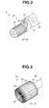
- an air/water feeding nozzle not illustrated are placed at the distal end portion 37 at which the US unit 30 that transmits and receives ultrasound is provided.
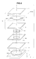
- an ultrasound array (a US array) 40 of the US unit 30 is a radial type transducer group in which long sides of a plurality of US elements 20 rectangular in plan view are connected and disposed to bend in a cylindrical shape. Namely, in the US array 40, 64 of the US elements 20 each with a short side of 0.1 mm or less are placed on a side surface of a cylinder with a diameter of 2 mm, for example.
- the US array 40 is a radial type transducer group, but the US array may be a convex type transducer group that is bent into a convex shape.
- the ultrasound transducer element 20 that is rectangular in plan view has a transmission and reception portion 60 in which a plurality of ultrasound cells 10 are two-dimensionally disposed in a matrix shape.
- a transmission and reception portion 60 in which a plurality of ultrasound cells 10 are two-dimensionally disposed in a matrix shape.
- an upper electrode terminal 51 and a lower electrode terminal 52 for driving the plurality of ultrasound cells 10 are placed.
- the plurality of US elements 20 have respective long sides connected to one another.
- a lower electrode portion 12A and an upper electrode portion 16A are disposed to face each other via a lower insulating layer 13, a gap adjusting portion 19, a cavity 14 and an upper insulating layer 15.
- a substrate side in a Z direction will be called a lower side
- a protection layer 17 side will be called an upper side.
- the US cell 10 has the lower electrode layer 12, the lower insulating layer 13, a gap adjusting layer 19A having the cavity 14, the upper insulating layer 15, the upper electrode layer 16 and the protection layer 17 that are stacked in sequence on a substrate 11 formed from silicon that is a base.
- a part 15B of the upper insulating layer 15 to the protection layer 17 that are directly over the cavity 14 configure a membrane 18.
- the membrane 18 is illustrated to be thick for explanation in Fig. 6 and the like, but is a vibration film of a small thickness of 1 ⁇ m to 10 ⁇ m, for example, which is stretched over an opening of the cavity 14 which is circular in plan view.
- the lower electrode layer 12 is formed by the lower electrode portion 12A and a lower wiring portion 12B.
- the upper electrode layer 16 is formed by the upper electrode portion 16A and an upper wiring portion 16B.
- the lower electrode portions 12A of all of the plurality of US cells 10 of the US element 20 are connected to the lower electrode terminal 52 via the lower wiring portions 12B.
- the upper electrode portions 16A of all of the plurality of US cells 10 of the US element 20 are connected to the upper electrode terminal 51 via the upper wiring portions 16B.
- the lower electrode portion 12A, the upper electrode portion 16A, the gap adjusting portion 19 and the cavity 14 are in rotationally symmetrical shape with respect to a center axis O, and are circular in plan view.
- the gap adjusting portion 19 that adjusts a gap that is a thickness (height) of the cavity 14, and is formed from a material with a high dielectric constant is placed on the lower insulating layer 13 in an inside of a cavity forming portion 14A that is a cylindrical cavity portion.
- a space of the cavity forming portion 14A that does not have the gap adjusting portion 19 is the cavity 14.
- a thickness "T" of the gap adjusting portion 19 is, for example, 0 ( ⁇ m) that is the smallest in a center portion, and monotonously increases in a curved manner toward an outer circumferential portion from the center portion.
- distribution T(r) of the thickness "T" of the gap adjusting portion 19 with a radius of "R” can be expressed by a function that is shown in (equation 1), for example, and monotonously increases in a curved manner toward the outer circumferential portion from the center portion.
- a distance from the center axis O is "r”
- the distribution T(r) does not have to correspond to the function shown in (equation 1) completely, and may have a little difference, for example, a difference of approximately ⁇ 5%.
- T r TR ⁇ 1 - J ⁇ 0 2.4 / R ⁇ r
- Equation 1 is an expression using a Bessel function of the zeroth kind that shows an envelope of vibration of a circular plane vibration plate the outer periphery of which is restrained.
- a thickness (height) "t” of the cavity 14 monotonously decreases in a curved manner toward the outer circumferential portion from a center O of the cavity 14 in response to thickness distribution of the gap adjusting portion 19, and is expressed by a Bessel function t(r) of the zeroth kind shown in (equation 2). Namely, the cavity 14 is in a so-called downward convex shape.
- t r t ⁇ 0 ⁇ J ⁇ 0 2.4 / R ⁇ r
- the thickness distribution (variation state) t(r) of the thickness "t" of the cavity 14 is the same as a theoretical deformation state of the membrane 18 when driven.
- a conductive layer formed from conductive silicon or a metal, for example, copper, gold, Mo, Ta or aluminum is deposited on an entire surface of the substrate 11 on which an insulating layer (not illustrated) is formed by a sputtering method, a CVD (chemical vapor deposition) method or the like. Subsequently, after a mask pattern formed from resist is formed on the conductive layer by photolithography, the conductive layer which is not covered with the mask pattern is selectively removed by etching, and thereby, the lower electrode layer 12 is formed.
- the lower insulating layer 13 formed from an insulating material such as SiN is deposited in such a manner as to cover the lower electrode layer 12 by a CVD method, for example.
- a surface of the lower insulating layer 13 is flattened by a CMP (chemical mechanical polish) method after deposition.
- an intermediate insulating layer 15A formed from SiN is further formed on the lower insulating layer 13.
- a thickness "t0 (TR)" of the intermediate insulating layer 15A corresponds to a thickness (height) of the cavity forming portion 14A.
- the intermediate insulating layer 15A is selectively removed by etching and the cavity forming portion 14A is formed.
- etching is performed with a chemical solution, gas or the like that selectively etches the intermediate insulating layer 15A.
- the surface of the intermediate insulating layer 15A is flattened by a CMP method in accordance with necessity, after which, only the cavity forming portion 14A may be etched until the cavity forming portion 14A has a maximum height (depth) "t0" of the cavity 14, based on an etching rate of the intermediate insulating layer 15A.
- the gap adjusting layer 19A formed from a material with a high dielectric constant is deposited on the surface of the intermediate insulating layer 15A to have a maximum thickness (height) "TR (t0)" of the cavity forming portion 14A, or more. Subsequently, a portion corresponding to a film thickness (convex portion) of the gap adjusting layer 19A is polished by a CMP method and a surface is flattened. Thereupon, a structure in which the gap adjusting layer 19A is buried only in the inside of the cavity forming portion 14A is produced.
- a photoresist is exposed via a gray scale photo-mask or the like, and thereby a resist mask 63 in which a thickness monotonously increases toward the outer circumferential portion from the center portion is produced.
- the thickness of the resist mask 63 monotonously increases in a curved manner toward the outer circumferential portion from the center portion as shown by (equation 1).
- Etch back processing is performed under dry etching conditions in which etching rates of the resist mask 63 and the gap adjusting layer 19A are equal to each other, whereby the gap adjusting portion 19 formed from a material with a high dielectric constant with a surface profile shown in (equation 1) is produced in the inside of the cavity forming portion 14A, as shown in Fig. 7C .
- a maximum thickness "t0 (TR)" of the sacrifice layer 61 after polishing is, for example, 0.05 ⁇ m to 0.3 ⁇ m, and preferably is 0.05 ⁇ m to 0.15 ⁇ m.
- the upper insulating layer 15 is formed by a similar method and from a similar material to the lower insulating layer 13, for example. Subsequently, at a predetermined position of the upper insulating layer 15, an opening portion (not illustrated) into which an etchant is poured is formed in order to remove the sacrifice layer 61.
- the sacrifice layer 61 is selectively removed by etching, and thereby the cavity 14 is formed.
- tungsten (W) is used as the sacrifice layer 61
- SiN is used as the lower insulating layer 13 and the upper insulating layer 15
- a hydrogen peroxide solution H 2 O 2
- conductive polycrystalline silicon is used as the sacrifice layer 61
- SiN is used as the lower insulating layer 13 and the upper insulating layer 15
- xenon fluoride gas (XeF 2 ) is used as the etchant.
- the upper electrode layer 16 is formed.
- the protection layer 17 has not only a protection function, but also a function of connecting the plurality of US elements 20.
- the protection layer 17 is formed from a flexible resin such as polyimide, epoxy, acryl, or poly-para-xylene, and among them, polyimide is preferable since polyimide has high chemical resistance and flexibility, and is easy to process.
- the protection layer 17 may be of a double layer structure in which a second insulating layer having biocompatibility is further formed on a first insulating layer.
- plan view of the cavity 14 does not have to be perfect circular, but may be substantially circular. Further, the plan view of the cavity 14 may be in a polygonal shape that is substantially circular. Namely, a shape of the cavity forming portion 14A is not limited to a circular cylinder shape, and may be a polygonal column shape or the like. When the cavity forming portion 14A is in a polygonal column shape, shapes in plan view of the upper electrode portion 16A and the lower electrode portion 12A are preferably also made polygonal. In the gap adjusting portion 19, a range of an inscribed circle can satisfy the thickness distribution.
- the plurality of US elements 20 are disposed by being bent into a radial shape in a connecting direction shown in Fig. 4 , and thereby the US array 40 shown in Fig. 2 and Fig. 3 is produced.
- the US array 40 is joined to an outer circumferential face of a cylinder with a predetermined outside diameter, for example. Further, a coaxial cable bundle 35 is connected to the US array 40, and the US unit 30 is produced.
- the lower electrode portion 12A is connected to a voltage signal generating section 3A of the ultrasound observation apparatus 3 via the lower electrode terminal 52.
- the upper electrode portion 16A is connected to a capacitive signal detecting section 3B via the upper electrode terminal 51 to be at a ground potential.
- the capacitive signal detecting section 3B detects a capacitive signal (a current change) at a time of receiving ultrasound.
- the voltage signal generating section 3A applies a drive voltage signal including a bias voltage to the lower electrode portion 12A.
- a voltage is applied to the lower electrode portion 12A
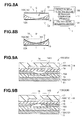
- the upper electrode portion 16A at a ground potential is attracted to the lower electrode portion 12A by an electrostatic force as shown in Fig. 8B , and therefore the membrane 18 including the upper electrode portion 16A deforms into a concave shape.
- the outer circumferential portion of the cavity 14 has a small height (thickness) "t", but does not interfere with deformation of the membrane 18, since a deformation amount of the outer circumferential portion of the membrane 18 is small.
- the cavity 14 of the conventional US element a whole of an inside thereof is made of air (vacuum) with a relative dielectric constant of "1 ", and the thickness thereof is the same and "t0" from the center portion to the outer circumferential portion.
- the cavity 14 of the conventional US element is the same as the cavity forming portion 14A of the US element 20.
- the gap adjusting portion 19 is placed in the inside of the cavity forming portion 14A of the US element 20.
- a relative dielectric constant Ks of the gap adjusting portion 19 formed from a material with a high dielectric coefficient is larger than "1". Therefore, a dielectric equivalent spacing "Teff' of the gap adjusting portion 19 is expressed by (equation 3) in a position at which the distance from a center of the cavity 14 is "r".
- the dielectric equivalent spacing "Teff' is an electrostatic spacing with the relative dielectric constant Ks taken into consideration with respect to a physical spacing "T".
- Teff r Tr r / Ks
- the dielectric equivalent spacing "Teff' can be regarded as substantially "zero". Namely, namely, in the US element 20, the gap adjusting portion 19 can be regarded as electrostatically absent.
- a physical spacing between the lower electrode portion 12A and the upper electrode portion 16A that are disposed to face each other via the cavity 14 is uniform.
- the ultrasound generated by the US cell 10 that deforms into a theoretical state becomes an ideal waveform with little distortion. Therefore, the US element 20 having the US cells 10 has favorable transmission efficiency of ultrasound.
- a gas may be held in the inside in a compressed state when the gas is present in the cavity 14, or may be released to an outside via an opening portion (not illustrated) that is formed to cause an etchant to flow therein, for example.
- the gap adjusting portion 19 formed from a material with a high dielectric coefficient with a higher insulating property than air is placed between the electrodes, and therefore, a withstand voltage between electrodes is high.
- the US element 20 having the US cells 10 has favorable reception efficiency of ultrasound.
- the electrostatic capacitance increases more than in the conventional US cell in which the distance between the electrodes is uniform. Therefore, in the US cell 10, a change rate of a charge amount increases even if the membrane 18 deforms to the extent that is the same as in the conventional US cell.
- the outer circumferential portion of the membrane 18 has a small deformation amount since the outer circumferential portion is restrained by the intermediate insulating layer 15A, but since the distance between the electrodes is short, the change in the charge amount is large.
- the US element 20 has favorable transmission and reception efficiency of ultrasound.
- the US endoscope 2 including the US element 20 has favorable transmission and reception efficiency of ultrasound.
- the thickness of the cavity is varied because the gap adjusting portion 19 that is formed from a material with a high dielectric constant in the inside of the cavity forming portion 14A that is a cylindrical cavity portion formed in the intermediate insulating layer 15A is placed.
- a part of the intermediate insulating layer 15A formed from a material with a high dielectric constant may be made a cavity 14A1 in which a thickness varies.
- a gap adjusting portion of a US element 20A of modification 1 of the first embodiment shown in Fig. 9A is a part of the intermediate insulating layer 15A.
- a cavity 14B of a US cell 10B of a US element 20B of modification 2 of the first embodiment is a so-called upward concave shape with a thickness thereof monotonously increasing in a curved manner toward an outer circumferential portion from a center portion similarly to that of the US element 20.
- the US element 20A and the US element 20B have the same effect as the US element 20.
- a thickness T12 of a lower electrode portion 12C that is covered with the lower insulating layer 13 increases monotonously in a curved manner toward an outer periphery from a center. Therefore, a physical spacing between the lower electrode portion 12C and the upper electrode portion 16A monotonously decreases in a curved manner toward an outer circumferential portion from a center. Therefore, a thickness "t" of a cavity 14C monotonously increases in a curved manner toward an outer circumferential portion from a center portion.
- Distribution of the thickness T12 of the lower electrode portion 12C of the US element 20C and distribution of the thickness "t" of the cavity 14C can be shown by a Bessel function of the zeroth kind of (equation 1) or (equation 2) similarly to the thickness variation of the gap adjusting portion 19 of the US element 20 of the first embodiment. Namely, in the US element 20C, a variation state of the thickness of the cavity 14C is the same as a deformation state of a membrane when driven.
- a top surface shape of the lower electrode portion 12C that is covered with the lower insulating layer 13 is the same as an undersurface shape of the cavity 14C.
- the lower electrode portion 12C is formed by performing etch back processing with use of a resist mask or the like in which a thickness monotonously increases toward an outer circumferential portion from a center portion similarly to the gap adjusting layer 19A.
- a convex portion a depth of which is expressed by a Bessel function of the zeroth kind, and monotonously decreases toward an outer circumferential portion from a center portion is formed in a substrate 11D, and a lower electrode portion 12D is formed thereon. Therefore, a physical spacing between the lower electrode portion 12A and the upper electrode portion 16D monotonously decreases in a curved manner toward the outer circumferential portion from a center.
- a thickness "t" of a cavity 14D monotonously increases in a curved manner toward the outer circumferential portion from the center portion.
- an upper electrode portion 16E is deformed into a convex shape that is expressed by a Bessel function of the zeroth kind by an internal stress of the membrane 18. Therefore, a physical spacing between the lower electrode portion 12A and an upper electrode portion 16E monotonously decreases in a curved manner toward an outer circumferential portion from a center. Therefore, a thickness "t" of a cavity 14E monotonously decreases in a curved manner toward the outer circumferential portion from the center portion.
- a US cell 10F of a US element 20F of modification 3 of the second embodiment shown in Fig. 10D has a cavity 14F in a double convex shape by a cavity in a downward convex shape that is expressed by a Bessel function of the zeroth kind, and a cavity in an upward convex shape that is expressed by a Bessel function of the zeroth kind being combined.
- a physical spacing between an upper electrode portion 16F and a lower electrode portion 12F on a substrate 11F monotonously decreases in a curved manner toward an outer circumferential portion from a center.
- the US elements 20C to 20F all have the same effect as the US element 20. Further, unlike the US element 20, the US elements 20C to 20F are easily produced since formation of the gap adjusting portion 19 is not necessary.
- the US elements 20A to 20F have favorable ultrasound transmission and reception efficiency similarly to the US element 20.
- the US endoscopes 2A to 2F including the US elements 20A to 20F have favorable ultrasound transmission and reception efficiency.
- the thickness (height) distribution t(r) of the cavities 14 to 14F shown in the first embodiment, the second embodiment and the modifications may be expressed by an arc function shown in (equation 5) or a sine function shown in (equation 6) if the thickness (height) distribution t(r) can be expressed by a function of the thickness "t" monotonously decreasing in a curved manner with increase of [r].
- t r t ⁇ 0 ⁇ 1 - r / R 2
- t r t ⁇ 0 ⁇ 1 - sin ⁇ / 2 ⁇ r / R
- the shape of the cavity is not limited to the shapes of the cavities 14 to 14F, and the thickness of the cavity may monotonously decrease in a curved manner toward the outer circumferential portion from the center portion.
- the top surface of the cavity may be bent significantly while the undersurface may be bent a little. Contrary to this, the top surface of the cavity may be bent a little, while the undersurface may be bent a little and significantly.
Landscapes
- Health & Medical Sciences (AREA)
- Life Sciences & Earth Sciences (AREA)
- Engineering & Computer Science (AREA)
- Surgery (AREA)
- Medical Informatics (AREA)
- Animal Behavior & Ethology (AREA)
- Radiology & Medical Imaging (AREA)
- Nuclear Medicine, Radiotherapy & Molecular Imaging (AREA)
- Biomedical Technology (AREA)
- Heart & Thoracic Surgery (AREA)
- Physics & Mathematics (AREA)
- Molecular Biology (AREA)
- Biophysics (AREA)
- Pathology (AREA)
- General Health & Medical Sciences (AREA)
- Public Health (AREA)
- Veterinary Medicine (AREA)
- Gynecology & Obstetrics (AREA)
- Mechanical Engineering (AREA)
- Optics & Photonics (AREA)
- Transducers For Ultrasonic Waves (AREA)
- Ultra Sonic Daignosis Equipment (AREA)
Abstract
Description
- The present invention relates to an electrostatic capacitive type ultrasound transducer element and an ultrasound endoscope including the ultrasound transducer element.
- An ultrasound diagnostic method that irradiates an inside of a body with ultrasound, and images a state of the inside of the body from an echo signal to perform diagnosis is widespread. One of the ultrasound diagnostic apparatuses for use in the ultrasound diagnostic method is an ultrasound endoscope (hereinafter, called "a US endoscope"). In a US endoscope, an ultrasound transducer is placed at a distal end rigid portion of an insertion portion that is introduced into an inside of a body. An ultrasound transducer has a function of converting an electric signal into ultrasound and transmitting the ultrasound to the inside of a body, and receiving ultrasound reflected in the inside of the body and converting the ultrasound into an electric signal.
- For an ultrasound transducer, a ceramic piezoelectric material containing lead that has large environmental load, for example, PZT (lead zirconate titanate) is mainly used. In contrast with this, development of an electrostatic capacitance type ultrasonic transducer (capacitive micro-machined ultrasonic transducer; hereinafter, called "a c-MUT") that does not contain lead in the material and is produced with use of MEMS (micro electro mechanical systems) technique is being advanced.
- As is disclosed in Japanese Patent Application Laid-Open Publication No.
2005-510264 - The US cell vibrates the membrane including the upper electrode portion by an electrostatic force by application of a voltage to between the lower electrode portion and the upper electrode portion to generate ultrasound. Further, when ultrasound is incident on the membrane from an outside, the membrane deforms to change a spacing of both the electrode portions, and therefore, the ultrasound is converted into an electric signal from a change in electrostatic capacitance.
- Here, since the membrane of a c-MUT is a circular film with an entire outer periphery fixed (restrained) similarly to a drumhead film, a center portion easily displaces, but an outer circumferential portion hardly displaces. Therefore, the outer circumferential portion of the membrane has lower transmission and reception efficiency as compared with the center portion. Namely, the conventional electrostatic capacitance type ultrasound transducer element and the ultrasound endoscope having the conventional electrostatic capacitance type ultrasound transducer element sometimes have not been able to be said to have favorable transmission and reception efficiency.
- The present invention has an object to provide an ultrasound transducer element with favorable transmission and reception efficiency and an ultrasound endoscope with favorable transmission and reception efficiency.
- An ultrasound transducer element of an embodiment of the present invention includes a plurality of electrostatic capacitance type ultrasound cells each having a lower electrode portion and a membrane including an upper electrode portion that are oriented and disposed via a cavity circular in plan view, wherein a thickness of the cavity monotonously decreases in a curved manner toward an outer circumferential portion from a center portion of the cavity.
- Further, an ultrasound endoscope of another embodiment includes an ultrasound transducer element having a plurality of electrostatic capacitance type ultrasound cells each having a lower electrode portion and a membrane including an upper electrode portion that are oriented and disposed via a cavity circular in plan view, wherein a thickness of the cavity monotonously decreases in a curved manner toward an outer circumferential portion from a center portion of the cavity.
-
-
Fig. 1 is an outside view for explaining an endoscope system including an ultrasound endoscope of a first embodiment; -
Fig. 2 is a perspective view for explaining a distal end portion of the ultrasound endoscope of the first embodiment; -
Fig. 3 is a perspective view for explaining a configuration of an ultrasound unit of the ultrasound endoscope of the first embodiment; -
Fig. 4 is a top view for explaining a configuration of an ultrasound transducer element of the first embodiment; -
Fig. 5 is a partial sectional view taken along a V-V line inFig. 4 ; -
Fig. 6 is an exploded view of an ultrasound cell of the ultrasound transducer element of the first embodiment; -
Fig. 7A is a partial sectional view for explaining a method for producing the ultrasound transducer element of the first embodiment; -
Fig. 7B is a partial sectional view for explaining the method for producing the ultrasound transducer element of the first embodiment; -
Fig. 7C is a partial sectional view for explaining the method for producing the ultrasound transducer element of the first embodiment; -
Fig. 7D is a partial sectional view for explaining the method for producing the ultrasound transducer element of the first embodiment; -
Fig. 7E is a partial sectional view for explaining the method for producing the ultrasound transducer element of the first embodiment; -
Fig. 8A is a schematic sectional view for explaining drive of the ultrasound transducer element of the first embodiment; -
Fig. 8B is a schematic sectional view for explaining drive of the ultrasound transducer element of the first embodiment; -
Fig. 9A is a partial sectional view of an ultrasound transducer element of modification 1 of the first embodiment; -
Fig. 9B is a partial sectional view of an ultrasound transducer element ofmodification 2 of the first embodiment; -
Fig. 10A is a partial sectional view of an ultrasound transducer element of a second embodiment; -
Fig. 10B is a partial sectional view of an ultrasound transducer element of modification 1 of the second embodiment; -
Fig. 10C is a partial sectional view of an ultrasound transducer element ofmodification 2 of the second embodiment; and -
Fig. 10D is a partial sectional view of an ultrasound transducer element ofmodification 3 of the second embodiment. - Hereinafter, an ultrasound transducer element (a US element) 20 of a first embodiment, and an ultrasound endoscope (hereinafter, called "a US endoscope") 2 having the US
element 20 will be described with reference to the drawings. - As shown in
Fig. 1 , the USendoscope 2 configures an ultrasound endoscope system 1 with anultrasound observation apparatus 3 and amonitor 4. The USendoscope 2 includes an elongated insertion portion 21 that is inserted into a body, anoperation portion 22 that is arranged at a proximal end of the insertion portion 21, and auniversal cord 23 that is extended from a side portion of theoperation portion 22. - At a proximal end portion of the
universal cord 23, aconnector 24A that is connected to a light source apparatus (not illustrated) is placed. From theconnector 24A, acable 25 that is detachably connected to a camera control unit (not illustrated) via aconnector 25A, and acable 26 that is detachably connected to theultrasound observation apparatus 3 via aconnector 26A are extended. Themonitor 4 is connected to theultrasound observation apparatus 3. - The insertion portion 21 is configured by a distal end rigid portion (hereinafter, called "a distal end portion") 37, a
bending portion 38 that is located at a rear end of thedistal end portion 37, and aflexible tube portion 39 that is located at a rear end of thebending portion 38 to reach theoperation portion 22, and has a small diameter, a long length and flexibility being connectively provided in sequence from a distal end side. At a distal end side of thedistal end portion 37, an ultrasound unit (a US unit) 30 that is an ultrasound transmitting and receiving portion is placed. - At the
operation portion 22, anangle knob 22A that performs bending control of thebending portion 38 in a desired direction, an air/water feeding button 22B that performs air feeding and water feeding operations, a suction button 22C that performs a suction operation, a treatmentinstrument insertion port 22D to be an inlet port for a treatment instrument that is introduced to an inside of a body and the like are placed. - As shown in
Fig. 2 , at thedistal end portion 37 at which theUS unit 30 that transmits and receives ultrasound is provided, anillumination lens cover 31 that configures an illumination optical system, anobservation lens cover 32 of an observation optical system, aforceps port 33 also used as a suction port, and an air/water feeding nozzle not illustrated are placed. - As shown in
Fig. 3 , an ultrasound array (a US array) 40 of theUS unit 30 is a radial type transducer group in which long sides of a plurality ofUS elements 20 rectangular in plan view are connected and disposed to bend in a cylindrical shape. Namely, in theUS array 40, 64 of theUS elements 20 each with a short side of 0.1 mm or less are placed on a side surface of a cylinder with a diameter of 2 mm, for example. - Note that the
US array 40 is a radial type transducer group, but the US array may be a convex type transducer group that is bent into a convex shape. - As shown in
Fig. 4 , theultrasound transducer element 20 that is rectangular in plan view has a transmission andreception portion 60 in which a plurality ofultrasound cells 10 are two-dimensionally disposed in a matrix shape. In each of theUS elements 20, anupper electrode terminal 51 and alower electrode terminal 52 for driving the plurality ofultrasound cells 10 are placed. The plurality ofUS elements 20 have respective long sides connected to one another. - Note that the drawings are all schematic views for explanation, and the numbers, the shapes, the thicknesses, and the dimensions of the patterns and the ratios of the sizes and the like differ from reality.
- As shown in
Fig. 5 andFig. 6 , in each of therespective US cells 10, alower electrode portion 12A and anupper electrode portion 16A are disposed to face each other via a lower insulatinglayer 13, agap adjusting portion 19, acavity 14 and an upper insulatinglayer 15. Note that hereinafter, a substrate side in a Z direction will be called a lower side, and aprotection layer 17 side will be called an upper side. - Namely, the
US cell 10 has thelower electrode layer 12, the lower insulatinglayer 13, agap adjusting layer 19A having thecavity 14, the upper insulatinglayer 15, theupper electrode layer 16 and theprotection layer 17 that are stacked in sequence on asubstrate 11 formed from silicon that is a base. A part 15B of the upper insulatinglayer 15 to theprotection layer 17 that are directly over thecavity 14 configure amembrane 18. Note that themembrane 18 is illustrated to be thick for explanation inFig. 6 and the like, but is a vibration film of a small thickness of 1 µm to 10 µm, for example, which is stretched over an opening of thecavity 14 which is circular in plan view. - The
lower electrode layer 12 is formed by thelower electrode portion 12A and alower wiring portion 12B. Further, theupper electrode layer 16 is formed by theupper electrode portion 16A and anupper wiring portion 16B. Thelower electrode portions 12A of all of the plurality ofUS cells 10 of theUS element 20 are connected to thelower electrode terminal 52 via thelower wiring portions 12B. Similarly, theupper electrode portions 16A of all of the plurality ofUS cells 10 of theUS element 20 are connected to theupper electrode terminal 51 via theupper wiring portions 16B. - Note that the
lower electrode portion 12A, theupper electrode portion 16A, thegap adjusting portion 19 and thecavity 14 are in rotationally symmetrical shape with respect to a center axis O, and are circular in plan view. - The
gap adjusting portion 19 that adjusts a gap that is a thickness (height) of thecavity 14, and is formed from a material with a high dielectric constant is placed on the lower insulatinglayer 13 in an inside of acavity forming portion 14A that is a cylindrical cavity portion. In other words, a space of thecavity forming portion 14A that does not have thegap adjusting portion 19 is thecavity 14. A thickness "T" of thegap adjusting portion 19 is, for example, 0 (µm) that is the smallest in a center portion, and monotonously increases in a curved manner toward an outer circumferential portion from the center portion. - Namely, distribution T(r) of the thickness "T" of the
gap adjusting portion 19 with a radius of "R" can be expressed by a function that is shown in (equation 1), for example, and monotonously increases in a curved manner toward the outer circumferential portion from the center portion. Here, a distance from the center axis O is "r", and a thickness of an outer periphery (r = R) of thegap adjusting portion 19 is "TR". As a matter of course, the distribution T(r) does not have to correspond to the function shown in (equation 1) completely, and may have a little difference, for example, a difference of approximately ±5%.
- J0 represents a Bessel function of the
order 0, J0(0) = 1 and J0(2.4) = 0. - Here, (equation 1) is an expression using a Bessel function of the zeroth kind that shows an envelope of vibration of a circular plane vibration plate the outer periphery of which is restrained.
- The
gap adjusting portion 19 is preferably formed from a material with a high dielectric constant, for example, SiO2 (Ks = 3.8) with a relative dielectric constant Ks being 3 or more, and especially preferably formed from SiN, for example, with a relative dielectric constant Ks being 5 or more. As a matter of course, Al2O3 (Ks = 8.5), Ta2O5 (Ks = 20 to 25), TiO2 (Ks = 40 to 110), HfOF, or HfO2, and further barium titanate ceramics or the like, which has a higher dielectric constant Ks, may be used, and from the viewpoint of easiness of a forming method and the like, the upper limit of the relative dielectric constant Ks is approximately 150. - A thickness (height) "t" of the
cavity 14 monotonously decreases in a curved manner toward the outer circumferential portion from a center O of thecavity 14 in response to thickness distribution of thegap adjusting portion 19, and is expressed by a Bessel function t(r) of the zeroth kind shown in (equation 2). Namely, thecavity 14 is in a so-called downward convex shape. Note that "t0" represents a thickness (height) "t" at the center (r = 0) of thecavity 14, and equals to the thickness "TR" of the outer periphery (r = R) of thegap adjusting portion 19.
- Namely, the thickness distribution (variation state) t(r) of the thickness "t" of the
cavity 14 is the same as a theoretical deformation state of themembrane 18 when driven. - Next, with use of
Fig. 7A to Fig. 7E , a method for producing theUS element 20 will be described. - A conductive layer formed from conductive silicon or a metal, for example, copper, gold, Mo, Ta or aluminum is deposited on an entire surface of the
substrate 11 on which an insulating layer (not illustrated) is formed by a sputtering method, a CVD (chemical vapor deposition) method or the like. Subsequently, after a mask pattern formed from resist is formed on the conductive layer by photolithography, the conductive layer which is not covered with the mask pattern is selectively removed by etching, and thereby, thelower electrode layer 12 is formed. - The lower insulating
layer 13 formed from an insulating material such as SiN is deposited in such a manner as to cover thelower electrode layer 12 by a CVD method, for example. In accordance with necessity, a surface of the lower insulatinglayer 13 is flattened by a CMP (chemical mechanical polish) method after deposition. Subsequently, an intermediate insulatinglayer 15A formed from SiN, for example, is further formed on the lower insulatinglayer 13. A thickness "t0 (TR)" of the intermediate insulatinglayer 15A corresponds to a thickness (height) of thecavity forming portion 14A. - As shown in
Fig. 7A , with use of a mask produced by a photolithography method, the intermediate insulatinglayer 15A is selectively removed by etching and thecavity forming portion 14A is formed. When the lower insulatinglayer 13 and the intermediate insulatinglayer 15A are formed from different materials, etching is performed with a chemical solution, gas or the like that selectively etches the intermediate insulatinglayer 15A. When the lower insulatinglayer 13 and the intermediate insulatinglayer 15A are formed from the same material, for example, SiN, the surface of the intermediate insulatinglayer 15A is flattened by a CMP method in accordance with necessity, after which, only thecavity forming portion 14A may be etched until thecavity forming portion 14A has a maximum height (depth) "t0" of thecavity 14, based on an etching rate of the intermediate insulatinglayer 15A. - The
gap adjusting layer 19A formed from a material with a high dielectric constant is deposited on the surface of the intermediate insulatinglayer 15A to have a maximum thickness (height) "TR (t0)" of thecavity forming portion 14A, or more. Subsequently, a portion corresponding to a film thickness (convex portion) of thegap adjusting layer 19A is polished by a CMP method and a surface is flattened. Thereupon, a structure in which thegap adjusting layer 19A is buried only in the inside of thecavity forming portion 14A is produced. - As shown in
Fig. 7B , a photoresist is exposed via a gray scale photo-mask or the like, and thereby a resistmask 63 in which a thickness monotonously increases toward the outer circumferential portion from the center portion is produced. Namely, the thickness of the resistmask 63 monotonously increases in a curved manner toward the outer circumferential portion from the center portion as shown by (equation 1). - Etch back processing is performed under dry etching conditions in which etching rates of the resist
mask 63 and thegap adjusting layer 19A are equal to each other, whereby thegap adjusting portion 19 formed from a material with a high dielectric constant with a surface profile shown in (equation 1) is produced in the inside of thecavity forming portion 14A, as shown inFig. 7C . - A sacrifice layer material composed of tungsten, for example, is deposited to a thickness of the maximum thickness (TR) of the
cavity forming portion 14A or more. Subsequently, when polishing by a CMP method is performed, a structure including asacrifice layer 61 in a cavity shape is obtained as shown inFig. 7D . A maximum thickness "t0 (TR)" of thesacrifice layer 61 after polishing is, for example, 0.05 µm to 0.3 µm, and preferably is 0.05 µm to 0.15 µm. - The upper insulating
layer 15 is formed by a similar method and from a similar material to the lower insulatinglayer 13, for example. Subsequently, at a predetermined position of the upper insulatinglayer 15, an opening portion (not illustrated) into which an etchant is poured is formed in order to remove thesacrifice layer 61. - The
sacrifice layer 61 is selectively removed by etching, and thereby thecavity 14 is formed. When tungsten (W) is used as thesacrifice layer 61, and SiN is used as the lower insulatinglayer 13 and the upper insulatinglayer 15, for example, a hydrogen peroxide solution (H2O2) is used as the etchant. Further, when conductive polycrystalline silicon is used as thesacrifice layer 61, and SiN is used as the lower insulatinglayer 13 and the upper insulatinglayer 15, xenon fluoride gas (XeF2) is used as the etchant. - By a method similar to the method for forming the
lower electrode layer 12, theupper electrode layer 16 is formed. - As shown in
Fig. 7E , the upper insulatinglayer 15 is covered with theprotection layer 17. Theprotection layer 17 has not only a protection function, but also a function of connecting the plurality ofUS elements 20. Theprotection layer 17 is formed from a flexible resin such as polyimide, epoxy, acryl, or poly-para-xylene, and among them, polyimide is preferable since polyimide has high chemical resistance and flexibility, and is easy to process. Note that theprotection layer 17 may be of a double layer structure in which a second insulating layer having biocompatibility is further formed on a first insulating layer. - Note that the plan view of the
cavity 14 does not have to be perfect circular, but may be substantially circular. Further, the plan view of thecavity 14 may be in a polygonal shape that is substantially circular. Namely, a shape of thecavity forming portion 14A is not limited to a circular cylinder shape, and may be a polygonal column shape or the like. When thecavity forming portion 14A is in a polygonal column shape, shapes in plan view of theupper electrode portion 16A and thelower electrode portion 12A are preferably also made polygonal. In thegap adjusting portion 19, a range of an inscribed circle can satisfy the thickness distribution. - The plurality of
US elements 20 are disposed by being bent into a radial shape in a connecting direction shown inFig. 4 , and thereby theUS array 40 shown inFig. 2 and Fig. 3 is produced. TheUS array 40 is joined to an outer circumferential face of a cylinder with a predetermined outside diameter, for example. Further, acoaxial cable bundle 35 is connected to theUS array 40, and theUS unit 30 is produced. - Next, an action of the
US element 20 will be described with use ofFig. 8A and Fig. 8B . Note that inFig. 8A and Fig. 8B , the lower insulatinglayer 13, the upper insulatinglayer 15, theprotection layer 17 and the like are not shown, and explanation of an influence thereof will be omitted. - As shown in
Fig. 8A , thelower electrode portion 12A is connected to a voltagesignal generating section 3A of theultrasound observation apparatus 3 via thelower electrode terminal 52. Theupper electrode portion 16A is connected to a capacitivesignal detecting section 3B via theupper electrode terminal 51 to be at a ground potential. The capacitivesignal detecting section 3B detects a capacitive signal (a current change) at a time of receiving ultrasound. - At a time of ultrasound generation (drive time), the voltage
signal generating section 3A applies a drive voltage signal including a bias voltage to thelower electrode portion 12A. When a voltage is applied to thelower electrode portion 12A, theupper electrode portion 16A at a ground potential is attracted to thelower electrode portion 12A by an electrostatic force as shown inFig. 8B , and therefore themembrane 18 including theupper electrode portion 16A deforms into a concave shape. Note that the outer circumferential portion of thecavity 14 has a small height (thickness) "t", but does not interfere with deformation of themembrane 18, since a deformation amount of the outer circumferential portion of themembrane 18 is small. - When voltage application to the
lower electrode portion 12A becomes nonexistent, themembrane 18 is restored to be in an original shape shown inFig. 8A by an elastic force. Ultrasound is generated by vibration by (deformation/restoration) of themembrane 18. - Here, in the
cavity 14 of the conventional US element, a whole of an inside thereof is made of air (vacuum) with a relative dielectric constant of "1 ", and the thickness thereof is the same and "t0" from the center portion to the outer circumferential portion. In other words, thecavity 14 of the conventional US element is the same as thecavity forming portion 14A of theUS element 20. - In contrast with this, the
gap adjusting portion 19 is placed in the inside of thecavity forming portion 14A of theUS element 20. A relative dielectric constant Ks of thegap adjusting portion 19 formed from a material with a high dielectric coefficient is larger than "1". Therefore, a dielectric equivalent spacing "Teff' of thegap adjusting portion 19 is expressed by (equation 3) in a position at which the distance from a center of thecavity 14 is "r". Here, the dielectric equivalent spacing "Teff' is an electrostatic spacing with the relative dielectric constant Ks taken into consideration with respect to a physical spacing "T".
- Here, when the relative dielectric constant Ks is sufficiently larger than "1", for example, in the case of Ks ≥ 3, the dielectric equivalent spacing "Teff' can be regarded as substantially "zero". Namely, namely, in the
US element 20, thegap adjusting portion 19 can be regarded as electrostatically absent. - Therefore, the dielectric equivalent spacing "teff' of the
cavity 14 can be expressed by being approximated by (equation 4).
- In other words, a physical spacing between the
lower electrode portion 12A and theupper electrode portion 16A that are disposed to face each other via thecavity 14 is uniform. However, the dielectric equivalent spacing "Teff' that is an effective thickness of thecavity 14, namely, the electrostatic spacing (effective distance between the electrodes) is the maximum at a center (r = 0), and decreases in a curved manner toward the outer circumferential portion. Since an electrostatic force is proportional to the effective distance between the electrodes, the electrostatic force that acts between the electrodes increases in theUS element 20 more than in the conventional US element in which the distance between the electrodes is uniform. Therefore, theUS element 20 has favorable generation efficiency of ultrasound. - Further, in the
US element 20, an entire undersurface of themembrane 18 that is attracted to thelower electrode portion 12A deforms in such a manner as to contact and stretch onto the top surface of thegap adjusting portion 19, when driven. Therefore, the deformation state of themembrane 18 when driven becomes the same as the shape of the top surface of thegap adjusting portion 19 shown by (equation 1) and the like. - As already described, the shape shown by (equation 1) or the like is a theoretical deformation shape of the vibration film.
- The ultrasound generated by the
US cell 10 that deforms into a theoretical state becomes an ideal waveform with little distortion. Therefore, theUS element 20 having theUS cells 10 has favorable transmission efficiency of ultrasound. - Note that when the entire undersurface of the
membrane 18 deforms significantly in such a manner as to stretch, namely, abut onto the top surface of thegap adjusting portion 19, a gas may be held in the inside in a compressed state when the gas is present in thecavity 14, or may be released to an outside via an opening portion (not illustrated) that is formed to cause an etchant to flow therein, for example. - Further, in the
US element 20, thegap adjusting portion 19 formed from a material with a high dielectric coefficient with a higher insulating property than air is placed between the electrodes, and therefore, a withstand voltage between electrodes is high. - The
US element 20 having theUS cells 10 has favorable reception efficiency of ultrasound. As is already described, in theUS cell 10 in which the distance between the electrodes decreases from the center portion to the outer circumferential portion, the electrostatic capacitance increases more than in the conventional US cell in which the distance between the electrodes is uniform. Therefore, in theUS cell 10, a change rate of a charge amount increases even if themembrane 18 deforms to the extent that is the same as in the conventional US cell. Furthermore, the outer circumferential portion of themembrane 18 has a small deformation amount since the outer circumferential portion is restrained by the intermediate insulatinglayer 15A, but since the distance between the electrodes is short, the change in the charge amount is large. - As in the above explanation, the
US element 20 has favorable transmission and reception efficiency of ultrasound. TheUS endoscope 2 including theUS element 20 has favorable transmission and reception efficiency of ultrasound. - As shown in
Fig. 8A and the like, in theUS element 20, the thickness of the cavity is varied because thegap adjusting portion 19 that is formed from a material with a high dielectric constant in the inside of thecavity forming portion 14A that is a cylindrical cavity portion formed in the intermediate insulatinglayer 15A is placed. In contrast with this, as in aUS cell 10A shown inFig. 9A , a part of the intermediate insulatinglayer 15A formed from a material with a high dielectric constant may be made a cavity 14A1 in which a thickness varies. Namely, a gap adjusting portion of aUS element 20A of modification 1 of the first embodiment shown inFig. 9A is a part of the intermediate insulatinglayer 15A. - Further, as shown in
Fig. 9B , acavity 14B of aUS cell 10B of aUS element 20B ofmodification 2 of the first embodiment is a so-called upward concave shape with a thickness thereof monotonously increasing in a curved manner toward an outer circumferential portion from a center portion similarly to that of theUS element 20. - The
US element 20A and theUS element 20B have the same effect as theUS element 20. - Hereinafter, with reference to the drawings, a
US element 20C having aUS cell 10C of a second embodiment will be described. Since theUS cell 10C and theUS element 20C are analogous to theUS cell 10 and theUS element 20 of the first embodiment, the same components will be assigned with the same reference signs, and explanation thereof will be omitted. - As shown in
Fig. 10A , in theUS cell 10C, a thickness T12 of alower electrode portion 12C that is covered with the lower insulatinglayer 13 increases monotonously in a curved manner toward an outer periphery from a center. Therefore, a physical spacing between thelower electrode portion 12C and theupper electrode portion 16A monotonously decreases in a curved manner toward an outer circumferential portion from a center. Therefore, a thickness "t" of acavity 14C monotonously increases in a curved manner toward an outer circumferential portion from a center portion. - Distribution of the thickness T12 of the
lower electrode portion 12C of theUS element 20C and distribution of the thickness "t" of thecavity 14C can be shown by a Bessel function of the zeroth kind of (equation 1) or (equation 2) similarly to the thickness variation of thegap adjusting portion 19 of theUS element 20 of the first embodiment. Namely, in theUS element 20C, a variation state of the thickness of thecavity 14C is the same as a deformation state of a membrane when driven. - In other words, a top surface shape of the
lower electrode portion 12C that is covered with the lower insulatinglayer 13 is the same as an undersurface shape of thecavity 14C. - The
lower electrode portion 12C is formed by performing etch back processing with use of a resist mask or the like in which a thickness monotonously increases toward an outer circumferential portion from a center portion similarly to thegap adjusting layer 19A. - As shown in
Fig. 10B , in aUS cell 10D of aUS element 20D of modification 1 of the second embodiment, a convex portion a depth of which is expressed by a Bessel function of the zeroth kind, and monotonously decreases toward an outer circumferential portion from a center portion is formed in asubstrate 11D, and alower electrode portion 12D is formed thereon. Therefore, a physical spacing between thelower electrode portion 12A and the upper electrode portion 16D monotonously decreases in a curved manner toward the outer circumferential portion from a center. A thickness "t" of acavity 14D monotonously increases in a curved manner toward the outer circumferential portion from the center portion. - Further, in a
US cell 10E of aUS element 20E ofmodification 2 of the second embodiment shown inFig. 10C , anupper electrode portion 16E is deformed into a convex shape that is expressed by a Bessel function of the zeroth kind by an internal stress of themembrane 18. Therefore, a physical spacing between thelower electrode portion 12A and anupper electrode portion 16E monotonously decreases in a curved manner toward an outer circumferential portion from a center. Therefore, a thickness "t" of acavity 14E monotonously decreases in a curved manner toward the outer circumferential portion from the center portion. - Furthermore, a
US cell 10F of aUS element 20F ofmodification 3 of the second embodiment shown inFig. 10D has acavity 14F in a double convex shape by a cavity in a downward convex shape that is expressed by a Bessel function of the zeroth kind, and a cavity in an upward convex shape that is expressed by a Bessel function of the zeroth kind being combined. A physical spacing between anupper electrode portion 16F and alower electrode portion 12F on asubstrate 11F monotonously decreases in a curved manner toward an outer circumferential portion from a center. - The
US elements 20C to 20F all have the same effect as theUS element 20. Further, unlike theUS element 20, theUS elements 20C to 20F are easily produced since formation of thegap adjusting portion 19 is not necessary. - As described above, the
US elements 20A to 20F have favorable ultrasound transmission and reception efficiency similarly to theUS element 20. TheUS endoscopes 2A to 2F including theUS elements 20A to 20F have favorable ultrasound transmission and reception efficiency. - Note that depending on the restraint conditions of the outer periphery of the
membrane 18, the thickness (height) distribution t(r) of thecavities 14 to 14F shown in the first embodiment, the second embodiment and the modifications may be expressed by an arc function shown in (equation 5) or a sine function shown in (equation 6) if the thickness (height) distribution t(r) can be expressed by a function of the thickness "t" monotonously decreasing in a curved manner with increase of [r].

- Further, the shape of the cavity is not limited to the shapes of the
cavities 14 to 14F, and the thickness of the cavity may monotonously decrease in a curved manner toward the outer circumferential portion from the center portion. For example, the top surface of the cavity may be bent significantly while the undersurface may be bent a little. Contrary to this, the top surface of the cavity may be bent a little, while the undersurface may be bent a little and significantly. - The present invention is not limited to the aforementioned embodiments, and various modifications, alterations and the like can be made within the range without departing from the gist of the present invention.
- The present application claims the benefit of Japanese Patent Application No.
2011-240475
Claims (10)
- An ultrasound transducer element, comprising:a plurality of electrostatic capacitance type ultrasound cells each having a lower electrode portion and a membrane including an upper electrode portion that are oriented and disposed via a cavity circular in plan view,wherein a thickness of the cavity monotonously decreases in a curved manner toward an outer circumferential portion from a center portion of the cavity.
- The ultrasound transducer element according to claim 1,
wherein a physical spacing or a dielectric equivalent spacing of the lower electrode portion and the upper electrode portion monotonously decreases in a curved manner toward the outer circumferential portion from the center portion. - The ultrasound transducer element according to claim 2,
wherein a variation state of the thickness of the cavity is the same as a deformation state of the membrane when driven. - The ultrasound transducer element according to claim 3,
wherein the variation state of the thickness of the cavity when driven is expressed by a Bessel function of the zeroth kind. - The ultrasound transducer element according to claim 4,
wherein a gap adjusting portion formed from a dielectric with a thickness thereof monotonously increasing in a curved manner toward an outer circumferential portion from a center portion is included between the lower electrode portion and the upper electrode portion. - The ultrasound transducer element according to claim 5,
wherein a relative dielectric constant of the dielectric is three or more. - The ultrasound transducer element according to claim 6,
wherein an undersurface of the membrane that is attracted to the lower electrode portion when driven contacts a top surface of the gap adjusting portion. - The ultrasound transducer element according to claim 4,
wherein a top surface shape of the lower electrode portion covered with a lower insulating layer is the same as an undersurface shape of the cavity. - The ultrasound transducer element according to claim 8,
wherein an undersurface of the membrane attracted to the lower electrode portion when driven contacts a top surface of the insulating layer. - An ultrasound endoscope, comprising:the ultrasound transducer element according to any one of claim 1 to claim 9.
Applications Claiming Priority (2)
| Application Number | Priority Date | Filing Date | Title |
|---|---|---|---|
| JP2011240475 | 2011-11-01 | ||
| PCT/JP2012/068603 WO2013065365A1 (en) | 2011-11-01 | 2012-07-23 | Ultrasonic oscillator element and ultrasonic endoscope |
Publications (3)
| Publication Number | Publication Date |
|---|---|
| EP2775736A1 true EP2775736A1 (en) | 2014-09-10 |
| EP2775736A4 EP2775736A4 (en) | 2015-08-05 |
| EP2775736B1 EP2775736B1 (en) | 2018-09-05 |
Family
ID=48191728
Family Applications (1)
| Application Number | Title | Priority Date | Filing Date |
|---|---|---|---|
| EP12844742.2A Not-in-force EP2775736B1 (en) | 2011-11-01 | 2012-07-23 | Ultrasonic oscillator element and ultrasonic endoscope |
Country Status (4)
| Country | Link |
|---|---|
| US (1) | US10016121B2 (en) |
| EP (1) | EP2775736B1 (en) |
| JP (1) | JP5669953B2 (en) |
| WO (1) | WO2013065365A1 (en) |
Families Citing this family (5)
| Publication number | Priority date | Publication date | Assignee | Title |
|---|---|---|---|---|
| EP2374474A1 (en) | 2005-01-19 | 2011-10-12 | Vaxinnate Corporation | Compositions comprising pathogen-associated molecular patterns and antigens and their use to stimulate an immune response |
| JP6763731B2 (en) * | 2016-09-28 | 2020-09-30 | 株式会社日立製作所 | Ultrasonic transducer, its manufacturing method and ultrasonic imaging device |
| WO2021038300A1 (en) * | 2019-08-30 | 2021-03-04 | Vermon Sa | Cmut transducer |
| CN113926679B (en) | 2020-06-29 | 2022-09-27 | 京东方科技集团股份有限公司 | Acoustic wave transduction unit, preparation method thereof and acoustic wave transducer |
| CN112427282B (en) * | 2020-10-28 | 2022-04-26 | 北京京东方技术开发有限公司 | Acoustic wave transduction unit, preparation method thereof and acoustic wave transducer |
Family Cites Families (13)
| Publication number | Priority date | Publication date | Assignee | Title |
|---|---|---|---|---|
| US5081995A (en) * | 1990-01-29 | 1992-01-21 | Mayo Foundation For Medical Education And Research | Ultrasonic nondiffracting transducer |
| US6556417B2 (en) * | 1998-03-10 | 2003-04-29 | Mcintosh Robert B. | Method to construct variable-area capacitive transducers |
| US6585653B2 (en) | 2001-07-31 | 2003-07-01 | Koninklijke Philips Electronics N.V. | Micro-machined ultrasonic transducer (MUT) array |
| WO2005120130A1 (en) * | 2004-06-03 | 2005-12-15 | Olympus Corporation | Electrostatic capacity type ultrasonic vibrator, manufacturing method thereof, and electrostatic capacity type ultrasonic probe |
| US20060004289A1 (en) * | 2004-06-30 | 2006-01-05 | Wei-Cheng Tian | High sensitivity capacitive micromachined ultrasound transducer |
| JP4746291B2 (en) * | 2004-08-05 | 2011-08-10 | オリンパス株式会社 | Capacitive ultrasonic transducer and manufacturing method thereof |
| JP2006122344A (en) * | 2004-10-28 | 2006-05-18 | Toshiba Corp | Ultrasound diagnostic imaging equipment |
| JP2008199341A (en) * | 2007-02-14 | 2008-08-28 | Seiko Epson Corp | Electrostatic transducer, ultrasonic speaker, speaker device, audio signal reproduction method using electrostatic transducer, directional acoustic system, and display device |
| JP5019997B2 (en) * | 2007-08-28 | 2012-09-05 | オリンパスメディカルシステムズ株式会社 | Ultrasonic transducer, ultrasonic diagnostic apparatus and ultrasonic microscope |
| US10092270B2 (en) * | 2007-09-17 | 2018-10-09 | Koninklijke Philips Electronics N.V. | Pre-collapsed CMUT with mechanical collapse retention |
| CN101896288B (en) * | 2007-12-14 | 2013-03-27 | 皇家飞利浦电子股份有限公司 | Collapsed mode operable CMUT including contoured substrate |
| US8531919B2 (en) * | 2009-09-21 | 2013-09-10 | The Hong Kong Polytechnic University | Flexible capacitive micromachined ultrasonic transducer array with increased effective capacitance |
| JP5550363B2 (en) * | 2010-01-26 | 2014-07-16 | キヤノン株式会社 | Capacitance type electromechanical transducer |
-
2012
- 2012-07-23 WO PCT/JP2012/068603 patent/WO2013065365A1/en not_active Ceased
- 2012-07-23 JP JP2013541655A patent/JP5669953B2/en active Active
- 2012-07-23 EP EP12844742.2A patent/EP2775736B1/en not_active Not-in-force
-
2014
- 2014-04-30 US US14/265,745 patent/US10016121B2/en active Active
Also Published As
| Publication number | Publication date |
|---|---|
| US20140236018A1 (en) | 2014-08-21 |
| JP5669953B2 (en) | 2015-02-18 |
| US10016121B2 (en) | 2018-07-10 |
| WO2013065365A1 (en) | 2013-05-10 |
| JPWO2013065365A1 (en) | 2015-04-02 |
| EP2775736A4 (en) | 2015-08-05 |
| EP2775736B1 (en) | 2018-09-05 |
Similar Documents
| Publication | Publication Date | Title |
|---|---|---|
| US10586912B2 (en) | Method for fabricating flexible micromachined transducer device | |
| JP4774393B2 (en) | Ultrasonic transducer, ultrasonic diagnostic apparatus and ultrasonic microscope | |
| JP4632853B2 (en) | Capacitive ultrasonic transducer and manufacturing method thereof | |
| EP2110186B1 (en) | Ultrasound transducer and electronic device | |
| US7995423B2 (en) | Ultrasound transducer and ultrasound diagnostic apparatus | |
| US20080089180A1 (en) | Ultrasonic transducer, ultrasonic probe, and ultrasonic diagnostic apparatus | |
| US10016121B2 (en) | Ultrasound transducer element and ultrasound endoscope | |
| US9629609B2 (en) | Ultrasound element and ultrasound endoscope | |
| JP5153972B2 (en) | Ultrasonic transducer and ultrasonic diagnostic apparatus | |
| WO2013005486A1 (en) | Electrostatic capacitance type ultrasonic transducer and electronic device | |
| JP2013034665A (en) | Ultrasonic element and ultrasonic endoscope | |
| US9636710B2 (en) | Ultrasound element and ultrasound endoscope | |
| JP4774394B2 (en) | Ultrasonic transducer, ultrasonic transducer manufacturing method, ultrasonic diagnostic apparatus, and ultrasonic microscope | |
| JP2011035916A (en) | Ultrasonic endoscope | |
| JP7816794B2 (en) | Flexible ultrasonic probe head, ultrasonic probe, and ultrasonic diagnostic device | |
| JP2008110059A (en) | Ultrasonic transducer, method for manufacturing ultrasonic transducer, and ultrasonic endoscope |
Legal Events
| Date | Code | Title | Description |
|---|---|---|---|
| PUAI | Public reference made under article 153(3) epc to a published international application that has entered the european phase |
Free format text: ORIGINAL CODE: 0009012 |
|
| 17P | Request for examination filed |
Effective date: 20140430 |
|
| AK | Designated contracting states |
Kind code of ref document: A1 Designated state(s): AL AT BE BG CH CY CZ DE DK EE ES FI FR GB GR HR HU IE IS IT LI LT LU LV MC MK MT NL NO PL PT RO RS SE SI SK SM TR |
|
| DAX | Request for extension of the european patent (deleted) | ||
| RA4 | Supplementary search report drawn up and despatched (corrected) |
Effective date: 20150703 |
|
| RIC1 | Information provided on ipc code assigned before grant |
Ipc: A61B 8/12 20060101ALI20150629BHEP Ipc: H04R 19/00 20060101AFI20150629BHEP |
|
| RAP1 | Party data changed (applicant data changed or rights of an application transferred) |
Owner name: OLYMPUS CORPORATION |
|
| RAP1 | Party data changed (applicant data changed or rights of an application transferred) |
Owner name: OLYMPUS CORPORATION |
|
| RAP1 | Party data changed (applicant data changed or rights of an application transferred) |
Owner name: OLYMPUS CORPORATION |
|
| RIN1 | Information on inventor provided before grant (corrected) |
Inventor name: WAKABAYASHI, KATSUHIRO Inventor name: MATSUMOTO, KAZUYA Inventor name: KARAKI, KAZUHISA Inventor name: HASEGAWA, MAMORU |
|
| STAA | Information on the status of an ep patent application or granted ep patent |
Free format text: STATUS: EXAMINATION IS IN PROGRESS |
|
| 17Q | First examination report despatched |
Effective date: 20170316 |
|
| GRAP | Despatch of communication of intention to grant a patent |
Free format text: ORIGINAL CODE: EPIDOSNIGR1 |
|
| STAA | Information on the status of an ep patent application or granted ep patent |
Free format text: STATUS: GRANT OF PATENT IS INTENDED |
|
| INTG | Intention to grant announced |
Effective date: 20180312 |
|
| RIN1 | Information on inventor provided before grant (corrected) |
Inventor name: WAKABAYASHI, KATSUHIRO Inventor name: MATSUMOTO, KAZUYA Inventor name: HASEGAWA, MAMORU Inventor name: KARAKI, KAZUHISA |
|
| GRAS | Grant fee paid |
Free format text: ORIGINAL CODE: EPIDOSNIGR3 |
|
| RIN1 | Information on inventor provided before grant (corrected) |
Inventor name: KARAKI, KAZUHISA Inventor name: WAKABAYASHI, KATSUHIRO Inventor name: HASEGAWA, MAMORU Inventor name: MATSUMOTO, KAZUYA |
|
| GRAA | (expected) grant |
Free format text: ORIGINAL CODE: 0009210 |
|
| STAA | Information on the status of an ep patent application or granted ep patent |
Free format text: STATUS: THE PATENT HAS BEEN GRANTED |
|
| AK | Designated contracting states |
Kind code of ref document: B1 Designated state(s): AL AT BE BG CH CY CZ DE DK EE ES FI FR GB GR HR HU IE IS IT LI LT LU LV MC MK MT NL NO PL PT RO RS SE SI SK SM TR |
|
| REG | Reference to a national code |
Ref country code: GB Ref legal event code: FG4D |
|
| REG | Reference to a national code |
Ref country code: CH Ref legal event code: EP |
|
| REG | Reference to a national code |
Ref country code: AT Ref legal event code: REF Ref document number: 1039320 Country of ref document: AT Kind code of ref document: T Effective date: 20180915 |
|
| REG | Reference to a national code |
Ref country code: IE Ref legal event code: FG4D |
|
| REG | Reference to a national code |
Ref country code: DE Ref legal event code: R096 Ref document number: 602012050799 Country of ref document: DE |
|
| REG | Reference to a national code |
Ref country code: NL Ref legal event code: MP Effective date: 20180905 |
|
| REG | Reference to a national code |
Ref country code: LT Ref legal event code: MG4D |
|
| PG25 | Lapsed in a contracting state [announced via postgrant information from national office to epo] |
Ref country code: FI Free format text: LAPSE BECAUSE OF FAILURE TO SUBMIT A TRANSLATION OF THE DESCRIPTION OR TO PAY THE FEE WITHIN THE PRESCRIBED TIME-LIMIT Effective date: 20180905 Ref country code: RS Free format text: LAPSE BECAUSE OF FAILURE TO SUBMIT A TRANSLATION OF THE DESCRIPTION OR TO PAY THE FEE WITHIN THE PRESCRIBED TIME-LIMIT Effective date: 20180905 Ref country code: SE Free format text: LAPSE BECAUSE OF FAILURE TO SUBMIT A TRANSLATION OF THE DESCRIPTION OR TO PAY THE FEE WITHIN THE PRESCRIBED TIME-LIMIT Effective date: 20180905 Ref country code: BG Free format text: LAPSE BECAUSE OF FAILURE TO SUBMIT A TRANSLATION OF THE DESCRIPTION OR TO PAY THE FEE WITHIN THE PRESCRIBED TIME-LIMIT Effective date: 20181205 Ref country code: LT Free format text: LAPSE BECAUSE OF FAILURE TO SUBMIT A TRANSLATION OF THE DESCRIPTION OR TO PAY THE FEE WITHIN THE PRESCRIBED TIME-LIMIT Effective date: 20180905 Ref country code: GR Free format text: LAPSE BECAUSE OF FAILURE TO SUBMIT A TRANSLATION OF THE DESCRIPTION OR TO PAY THE FEE WITHIN THE PRESCRIBED TIME-LIMIT Effective date: 20181206 Ref country code: NO Free format text: LAPSE BECAUSE OF FAILURE TO SUBMIT A TRANSLATION OF THE DESCRIPTION OR TO PAY THE FEE WITHIN THE PRESCRIBED TIME-LIMIT Effective date: 20181205 |
|
| REG | Reference to a national code |
Ref country code: AT Ref legal event code: MK05 Ref document number: 1039320 Country of ref document: AT Kind code of ref document: T Effective date: 20180905 |
|
| PG25 | Lapsed in a contracting state [announced via postgrant information from national office to epo] |
Ref country code: HR Free format text: LAPSE BECAUSE OF FAILURE TO SUBMIT A TRANSLATION OF THE DESCRIPTION OR TO PAY THE FEE WITHIN THE PRESCRIBED TIME-LIMIT Effective date: 20180905 Ref country code: LV Free format text: LAPSE BECAUSE OF FAILURE TO SUBMIT A TRANSLATION OF THE DESCRIPTION OR TO PAY THE FEE WITHIN THE PRESCRIBED TIME-LIMIT Effective date: 20180905 Ref country code: AL Free format text: LAPSE BECAUSE OF FAILURE TO SUBMIT A TRANSLATION OF THE DESCRIPTION OR TO PAY THE FEE WITHIN THE PRESCRIBED TIME-LIMIT Effective date: 20180905 |
|
| PG25 | Lapsed in a contracting state [announced via postgrant information from national office to epo] |
Ref country code: NL Free format text: LAPSE BECAUSE OF FAILURE TO SUBMIT A TRANSLATION OF THE DESCRIPTION OR TO PAY THE FEE WITHIN THE PRESCRIBED TIME-LIMIT Effective date: 20180905 Ref country code: AT Free format text: LAPSE BECAUSE OF FAILURE TO SUBMIT A TRANSLATION OF THE DESCRIPTION OR TO PAY THE FEE WITHIN THE PRESCRIBED TIME-LIMIT Effective date: 20180905 Ref country code: IS Free format text: LAPSE BECAUSE OF FAILURE TO SUBMIT A TRANSLATION OF THE DESCRIPTION OR TO PAY THE FEE WITHIN THE PRESCRIBED TIME-LIMIT Effective date: 20190105 Ref country code: ES Free format text: LAPSE BECAUSE OF FAILURE TO SUBMIT A TRANSLATION OF THE DESCRIPTION OR TO PAY THE FEE WITHIN THE PRESCRIBED TIME-LIMIT Effective date: 20180905 Ref country code: EE Free format text: LAPSE BECAUSE OF FAILURE TO SUBMIT A TRANSLATION OF THE DESCRIPTION OR TO PAY THE FEE WITHIN THE PRESCRIBED TIME-LIMIT Effective date: 20180905 Ref country code: RO Free format text: LAPSE BECAUSE OF FAILURE TO SUBMIT A TRANSLATION OF THE DESCRIPTION OR TO PAY THE FEE WITHIN THE PRESCRIBED TIME-LIMIT Effective date: 20180905 Ref country code: IT Free format text: LAPSE BECAUSE OF FAILURE TO SUBMIT A TRANSLATION OF THE DESCRIPTION OR TO PAY THE FEE WITHIN THE PRESCRIBED TIME-LIMIT Effective date: 20180905 Ref country code: CZ Free format text: LAPSE BECAUSE OF FAILURE TO SUBMIT A TRANSLATION OF THE DESCRIPTION OR TO PAY THE FEE WITHIN THE PRESCRIBED TIME-LIMIT Effective date: 20180905 Ref country code: PL Free format text: LAPSE BECAUSE OF FAILURE TO SUBMIT A TRANSLATION OF THE DESCRIPTION OR TO PAY THE FEE WITHIN THE PRESCRIBED TIME-LIMIT Effective date: 20180905 |
|
| PG25 | Lapsed in a contracting state [announced via postgrant information from national office to epo] |
Ref country code: PT Free format text: LAPSE BECAUSE OF FAILURE TO SUBMIT A TRANSLATION OF THE DESCRIPTION OR TO PAY THE FEE WITHIN THE PRESCRIBED TIME-LIMIT Effective date: 20190105 Ref country code: SM Free format text: LAPSE BECAUSE OF FAILURE TO SUBMIT A TRANSLATION OF THE DESCRIPTION OR TO PAY THE FEE WITHIN THE PRESCRIBED TIME-LIMIT Effective date: 20180905 Ref country code: SK Free format text: LAPSE BECAUSE OF FAILURE TO SUBMIT A TRANSLATION OF THE DESCRIPTION OR TO PAY THE FEE WITHIN THE PRESCRIBED TIME-LIMIT Effective date: 20180905 |
|
| REG | Reference to a national code |
Ref country code: DE Ref legal event code: R097 Ref document number: 602012050799 Country of ref document: DE |
|
| PLBE | No opposition filed within time limit |
Free format text: ORIGINAL CODE: 0009261 |
|
| STAA | Information on the status of an ep patent application or granted ep patent |
Free format text: STATUS: NO OPPOSITION FILED WITHIN TIME LIMIT |
|
| PG25 | Lapsed in a contracting state [announced via postgrant information from national office to epo] |
Ref country code: DK Free format text: LAPSE BECAUSE OF FAILURE TO SUBMIT A TRANSLATION OF THE DESCRIPTION OR TO PAY THE FEE WITHIN THE PRESCRIBED TIME-LIMIT Effective date: 20180905 |
|
| 26N | No opposition filed |
Effective date: 20190606 |
|
| PG25 | Lapsed in a contracting state [announced via postgrant information from national office to epo] |
Ref country code: SI Free format text: LAPSE BECAUSE OF FAILURE TO SUBMIT A TRANSLATION OF THE DESCRIPTION OR TO PAY THE FEE WITHIN THE PRESCRIBED TIME-LIMIT Effective date: 20180905 |
|
| PGFP | Annual fee paid to national office [announced via postgrant information from national office to epo] |
Ref country code: DE Payment date: 20190725 Year of fee payment: 8 |
|
| PG25 | Lapsed in a contracting state [announced via postgrant information from national office to epo] |
Ref country code: MC Free format text: LAPSE BECAUSE OF FAILURE TO SUBMIT A TRANSLATION OF THE DESCRIPTION OR TO PAY THE FEE WITHIN THE PRESCRIBED TIME-LIMIT Effective date: 20180905 |
|
| REG | Reference to a national code |
Ref country code: CH Ref legal event code: PL |
|
| GBPC | Gb: european patent ceased through non-payment of renewal fee |
Effective date: 20190723 |
|
| PG25 | Lapsed in a contracting state [announced via postgrant information from national office to epo] |
Ref country code: TR Free format text: LAPSE BECAUSE OF FAILURE TO SUBMIT A TRANSLATION OF THE DESCRIPTION OR TO PAY THE FEE WITHIN THE PRESCRIBED TIME-LIMIT Effective date: 20180905 |
|
| REG | Reference to a national code |
Ref country code: BE Ref legal event code: MM Effective date: 20190731 |
|
| PG25 | Lapsed in a contracting state [announced via postgrant information from national office to epo] |
Ref country code: GB Free format text: LAPSE BECAUSE OF NON-PAYMENT OF DUE FEES Effective date: 20190723 |
|
| PG25 | Lapsed in a contracting state [announced via postgrant information from national office to epo] |
Ref country code: LI Free format text: LAPSE BECAUSE OF NON-PAYMENT OF DUE FEES Effective date: 20190731 Ref country code: CH Free format text: LAPSE BECAUSE OF NON-PAYMENT OF DUE FEES Effective date: 20190731 Ref country code: BE Free format text: LAPSE BECAUSE OF NON-PAYMENT OF DUE FEES Effective date: 20190731 Ref country code: LU Free format text: LAPSE BECAUSE OF NON-PAYMENT OF DUE FEES Effective date: 20190723 |
|
| PG25 | Lapsed in a contracting state [announced via postgrant information from national office to epo] |
Ref country code: FR Free format text: LAPSE BECAUSE OF NON-PAYMENT OF DUE FEES Effective date: 20190731 |
|
| PG25 | Lapsed in a contracting state [announced via postgrant information from national office to epo] |
Ref country code: IE Free format text: LAPSE BECAUSE OF NON-PAYMENT OF DUE FEES Effective date: 20190723 |
|
| REG | Reference to a national code |
Ref country code: DE Ref legal event code: R119 Ref document number: 602012050799 Country of ref document: DE |
|
| PG25 | Lapsed in a contracting state [announced via postgrant information from national office to epo] |
Ref country code: CY Free format text: LAPSE BECAUSE OF FAILURE TO SUBMIT A TRANSLATION OF THE DESCRIPTION OR TO PAY THE FEE WITHIN THE PRESCRIBED TIME-LIMIT Effective date: 20180905 Ref country code: DE Free format text: LAPSE BECAUSE OF NON-PAYMENT OF DUE FEES Effective date: 20210202 |
|
| PG25 | Lapsed in a contracting state [announced via postgrant information from national office to epo] |
Ref country code: MT Free format text: LAPSE BECAUSE OF FAILURE TO SUBMIT A TRANSLATION OF THE DESCRIPTION OR TO PAY THE FEE WITHIN THE PRESCRIBED TIME-LIMIT Effective date: 20180905 Ref country code: HU Free format text: LAPSE BECAUSE OF FAILURE TO SUBMIT A TRANSLATION OF THE DESCRIPTION OR TO PAY THE FEE WITHIN THE PRESCRIBED TIME-LIMIT; INVALID AB INITIO Effective date: 20120723 |
|
| PG25 | Lapsed in a contracting state [announced via postgrant information from national office to epo] |
Ref country code: MK Free format text: LAPSE BECAUSE OF FAILURE TO SUBMIT A TRANSLATION OF THE DESCRIPTION OR TO PAY THE FEE WITHIN THE PRESCRIBED TIME-LIMIT Effective date: 20180905 |